Applications of Oxide Coatings in Photovoltaic Devices

PVcomB, Helmholtz-Zentrum Berlin für Materialien und Energie GmbH, Hahn-Meintner Platz 1, 14109 Berlin, Germany
Coatings 2014, 4(1), 162-202; https://doi.org/10.3390/coatings4010162
Submission received: 10 February 2014
/
Accepted: 10 March 2014
/
Published: 24 March 2014
(This article belongs to the Special Issue Novel Thin Film Materials for Photovoltaic Applications)
Abstract
:Metalloid and metal based oxides are an almost unavoidable component in the majority of solar cell technologies used at the time of writing this review. Numerous studies have shown increases of ≥1% absolute in solar cell efficiency by simply substituting a given layer in the material stack with an oxide. Depending on the stoichiometry and whether other elements are present, oxides can be used for the purpose of light management, passivation of electrical defects, photo-carrier generation, charge separation, and charge transport in a solar cell. In this review, the most commonly used oxides whose benefits for solar cells have been proven both in a laboratory and industrial environment are discussed. Additionally, developing trends in the use of oxides, as well as newer oxide materials, and deposition technologies for solar cells are reported.
1. Introduction
Many review articles about oxides have been published but most of them concentrate on specific properties such as electrical conductivity [1], simultaneously high optical transparency and electrical conductivity [2], photoconductivity [3], dielectric constant [4], catalysis [5], electronic structure [6], among others. The wide range of properties of oxides, not only suggests, but demonstrates the versatility of oxides as functional materials. Indeed, the potential of these important materials can be exploited to enhance the performance of opto-electronic devices such as photovoltaic (PV) cells. It follows that an assessment of the various oxides available and how their properties can be used in PV cells would be useful for the researcher looking to enhance the photo-conversion efficiencies above the present day levels while keeping the device cost as low as possible. In general, different materials are required to perform different functions in a PV cell, namely:
- The absorber is responsible for absorption and conversion of incident photons to charge carriers;
- Electrodes are necessary to convey the photo-generated carriers to an external load;
- Antireflection coatings (ARCs) are applied to PV cells to ensure a gradual increase of the refractive index as incident photons traverse from air through to the absorber so as to reduce the backward reflection losses;
- Back reflectors are used to prevent energy waste when the absorber is too thin to absorb all the incident photons in one pass;
- Buffers and/or barriers are used to prevent irregularities at interfaces from affecting PV cell performance. These may be defect states caused by lattice mismatch, too large energy band offsets or diffusion of contaminants into the absorber, among others.
2. Ideal Material Characteristics for Various Functions in PV Cells
In order to identify those oxides that are suitable for use in PV cells, it is important to familiarise oneself with the ideal material requirements for high power conversion efficiency (PCE). All PV cells consist basically of a semiconductor material capable of absorbing a certain portion of the solar spectrum and adjacent layers (electrodes) required to extract the photo-generated carriers for conveyance to an external electrical load. Therefore, the optical and electronic properties of each material in the PV cell should be tuned to prevent unnecessary loss of incident photons through reflection and parasitic absorption, as well as, to minimise loss of the photo-generated power via recombination at trap states and electrical resistance losses. Additionally, the PV cells should maintain their initial efficiency over a lifetime of at least 20 years and should therefore not only be mechanically stable, but also resistant to degradation caused by exposure to the environment.
2.1. Appropriate Opto-Electronic Properties
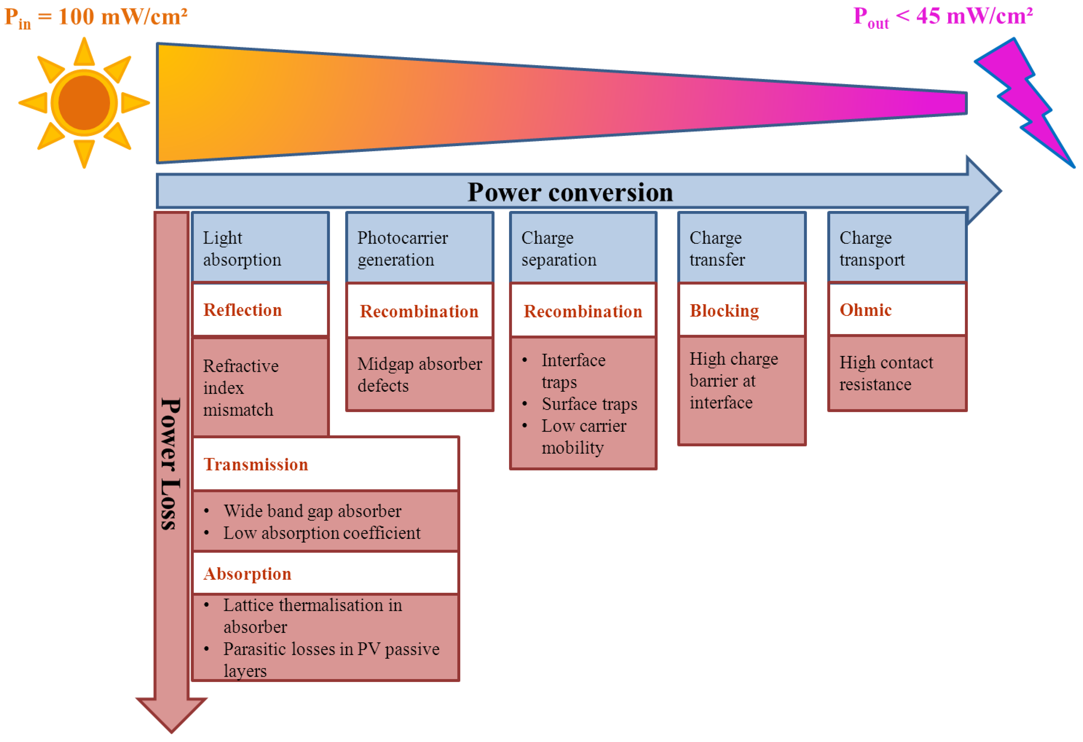
The main power conversion and power loss processes in a PV cell are illustrated in the schematic in Figure 1. The first key condition for high PCE is that the photoactive (absorber) layer has a narrow enough band-gap (around 1–2 eV) to absorb photons with a wide range of energies, most especially, in that portion of the solar irradiance with high intensity. The second key condition is that as many as possible incident photons enter the photoactive layer (absorber) of the device for conversion into charge carriers. This requires that all other “photo-passive” but functional layers in the PV cell that lie in the path of photons traversing to the absorber should not absorb or back reflect any of the light before it reaches the absorber. That is, the window layers must be highly transparent i.e., have a wider band gap than the absorber and thus a much lower absorption coefficient in the spectral range of light used for photo-conversion. Where reflection losses are undesirable, the functional layer must have a refractive index close to that of the absorber material.
Electrically, the components of the PV cell should minimise recombination of photo-generated electrons and holes in order to maximise the photocurrent. As a consequence, the absorber must have a low defect density so that the minority carriers have a long enough life-time to transverse to the electrodes for collection. Also, the materials adjacent to the absorber should have a small conduction band (CB) or valence band (VB) offset for electron and hole transfer, respectively, across the interface and be free from trap states that would enhance recombination of the photo-generated carriers. In order to collect as many of the photo-generated carriers as possible for use in an external load, the terminal contacts/electrodes of the PV device should be highly conductive. High conductivity requires high hole/electron mobility and/or high hole/electron density, or both. However, as will be discussed later, there are some instances when an insulating layer is required to prevent recombination of photo-generated carriers before they can be used to drive an external load. In this case, the insulating layer should be very thin to allow passage of photo-generated carriers via tunnelling. On the other hand, the absorber should have an appropriately wide band-gap to ensure the highest possible value of the photo-generated voltage which is in conflict with the requirement for maximal photon absorption. The junction should be of a strongly rectifying behavior to prevent shunting which would reduce the voltage of the PV cell. Additionally, the photo-generated voltage should be maintained as high as possible by optimising the energy band offsets at different interfaces of the PV cells. The terminal voltage of the cell should further be preserved by avoiding resistive losses in the contacts/electrodes.
Figure 1.
Power conversion and power loss processes in a photovoltaic (PV) cell. Each of the losses can occur at several interfaces and regions of the PV cell. The maximum power output is based on the current experimental efficiency record [7].
Figure 1.
Power conversion and power loss processes in a photovoltaic (PV) cell. Each of the losses can occur at several interfaces and regions of the PV cell. The maximum power output is based on the current experimental efficiency record [7].

2.2. Suitability for Manufacturing
In order for materials that show promisingly high photo-electrical conversion efficiency in the laboratory, to be implemented in commercial products, they must be compatible with certain technical demands. The first criterion for the adaptation of a material into a commercial product is the cost involved either in purchasing of raw materials, processing and yield or even in environmentally friendly end-of-life disposal. The abundance of a material in the earth’s crust contributes significantly to the material costs, such that most abundant elements are relatively inexpensive. In this respect, the wide use of oxides in PV cells may be attributed to the fact that oxygen is the most abundant element on the earth. Similarly, since silicon is the second most abundant material and arguably the most abundant elemental photo-active material it is not surprising that it is the dominant material for photovoltaic cells.
However, abundance does not always directly translate to lower material cost as extraction of a given element from its natural form or ore, may involve energy intensive processes that translate to a higher price than less abundant materials. Therefore, the simplest way to minimise material costs would be to use as little as possible of the material for a given function. This means that the absorber should ideally have a direct band gap and a high absorption coefficient so that minimal material is required in the PV cell. Similarly, the electrodes must be highly conductive so that very thin layers are sufficient to transport the photo-current with minimum resistance losses. Less energy intensive processing using solutions carried out at atmospheric pressure and at reasonably low temperatures are preferable to vacuum processing and high temperature processing, although in most cases the material properties are inferior despite the lower processing costs. As the volumes of PV cells increase drastically, or when hazardous components are unavoidable, the cost of recycling or disposal at the end of the device’s life may become a significant fraction of the overall PV cell costs.
2.3. Toxicity and Environmental Benignity
It is important that not only the materials used in a PV cell are non-toxic but that also the manufacturing processes thereof are environmentally benign. This requirement is also in harmony with the “green” philosophy which is meant to make photovoltaics competitive in comparison to other energy generating technologies such as nuclear power and fossil fuels. The use of several hazardous elements such as Cd, Pb, Hg and the radioactive elements including, Po and Ur, among others, in devices appropriate for the public market is severely restricted. Additionally, while the oxides of essentially poisonous elements may themselves be considered to be non-hazardous because of their chemical stability, some oxides such as BeO are toxic.
2.4. Environmental and Chemical Stability
PV cells are expected to deliver the nameplate output for at least 20 years after installation in the field and thus failure of the device before this duration is to be avoided. In service, perhaps the biggest threat to PV cells from the environment is moisture, which accelerates oxidation of the different components. The PV cell material components should therefore resist degradation by air (oxygen), moisture and impurity diffusion. Where the materials are not environmentally/chemically resistant, an encapsulation and/barrier should be provided to protect them. However, although PV cells in the field are encapsulated to prevent moisture ingress, it is preferred that the device should still be somewhat stable to the environment to extend its lifetime in case the encapsulation gets damaged. For PV cells grown on glass, the diffusion of sodium into the PV cell is of particular concern as it is accelerated by the presence of a bias voltage [8]. Interdiffusion of elements from sources internal to the PV cell device may also be detrimental to the PV cell performance, necessitating diffusion barriers.
3. Survey of Oxides with Proven or Potential Application in PV Cells
Oxygen is a group 16 (also known as chalcogens) element and exists in pure form as a diatom O2 or as ozone O3. The most common form is the diatomic molecule O2 which contains two unpaired electrons hence the double covalent bonding and is therefore paramagnetic. Oxygen has several oxidation states namely O−2, ![Coatings 04 00162 i001]() and
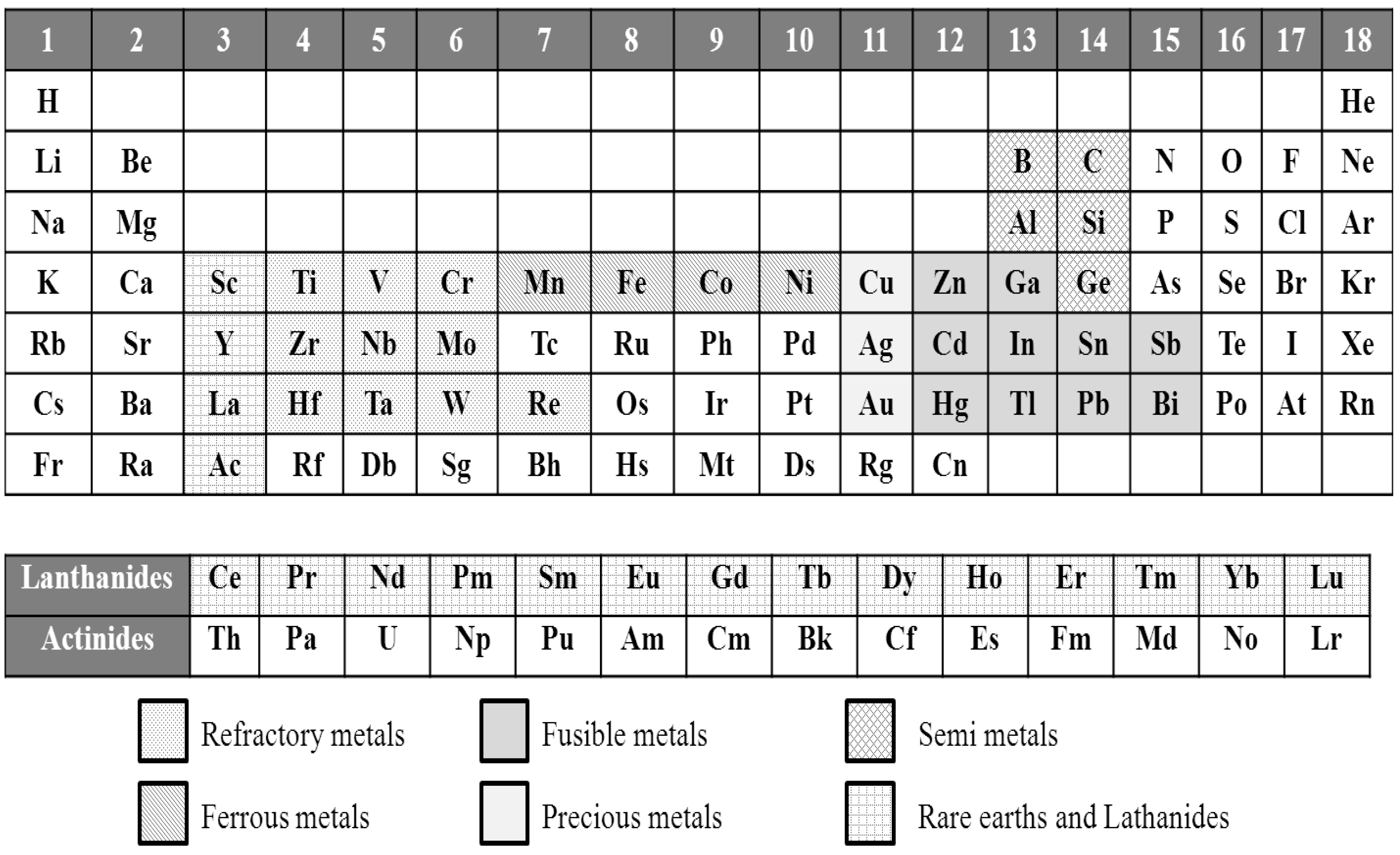
and ![Coatings 04 00162 i002]() corresponding to oxides, peroxides and super oxides. Typically, an oxide is formed when a metal/metalloid donates two electrons to the 2p orbital of the oxygen atom such that the oxygen orbitals form the valence band of the resulting oxide. Since this review is confined to solid state photovoltaic devices, only solid oxides are considered. The type of oxide formed depends to a large extent on the position of the bonding cation in the periodic table (see Figure 2).
corresponding to oxides, peroxides and super oxides. Typically, an oxide is formed when a metal/metalloid donates two electrons to the 2p orbital of the oxygen atom such that the oxygen orbitals form the valence band of the resulting oxide. Since this review is confined to solid state photovoltaic devices, only solid oxides are considered. The type of oxide formed depends to a large extent on the position of the bonding cation in the periodic table (see Figure 2).
 and
and  corresponding to oxides, peroxides and super oxides. Typically, an oxide is formed when a metal/metalloid donates two electrons to the 2p orbital of the oxygen atom such that the oxygen orbitals form the valence band of the resulting oxide. Since this review is confined to solid state photovoltaic devices, only solid oxides are considered. The type of oxide formed depends to a large extent on the position of the bonding cation in the periodic table (see Figure 2).
Figure 2.
Periodic table of elements. For convenience, technologically relevant classifications [9] of elements with similar properties transcend the periodic groups as shown in the shaded areas.
Figure 2.
Periodic table of elements. For convenience, technologically relevant classifications [9] of elements with similar properties transcend the periodic groups as shown in the shaded areas.

For instance, the acidity of the oxide increases with the cation charge i.e. going left of and/or up the periodic table. Similarly, the electrical conduction depends on the type of bond between the cation and the oxygen especially as far as which electrons are involved in the bonding [10]. Oxides with ionic bonds typically have a high dielectric constant and are usually insulating while those with more covalent bonds have a narrower optical band gap and are capable of becoming semiconducting under certain circumstances. At first glance, many stoichiometric oxides do not fulfil the functional requirements for PV cells. However, sub-stoichiometry, either hypo-(excess cation) or hyper-(excess oxygen) stoichiometry combined, at times, with doping may introduce wide variations in the metal oxide properties making them suitable for a wide palate of functionalities. Theoretical calculations supported by experimental evidence from X-ray absorption spectroscopy XAS, high resolution X-ray photoelectron spectroscopy XPS and X-ray emission spectroscopy XES, among others have given insights into the electronic band structure of different oxide materials and have been useful in understanding their material properties and in identifying new oxides for use in PV devices.
Most elements have multiple oxides corresponding to various oxidation states [11]. Moreover for the same oxidation state, slight differences in stoichiometry and/or coordination structure lead to different phases with markedly different physical properties. For conciseness, in this work, only those oxides known or identified as useful components of PV cells are described. Such oxides tend to invariably be the most thermodynamically stable form since the processing of PV cells involves different steps with various temperature regimes. Further discussion of oxides shall be confined to those elements in the periodic table which have been cited in the literature in connection with a working PV cell device. Because of gradual variations across and down the periodic table, it is also convenient to group the oxides to be discussed using a classification that combines those elements with similar properties i.e.,: alkali metals (all group 1), alkali-earth metals (all goup 2), rare earths and lanthanides (Sc, Y, La and the lanthanides), refractory metals (Ti, Zr, Hf, V, Nb, Ta, Cr, Mo, W and Re), ferrous metals (Mn, Fe, Co and Ni), precious metals (Cu,Ag, Au), fusible metals (Zn, Cd, Hg, Ga, In, Tl, Sn, Pb, Sb, Bi) and semimetals (B, Al, C, Si, Ge). Alkali-earth metals cover all group 2 elements but since their oxides are very reactive with water, they are of little interest for PV cell devices since processing would be difficult to handle. The oxides of rare earth and lanthanide elements are discussed later in Section 6 as they are an emerging material for PV cells.
3.1. Refractory Metal Oxides
The refractory metals consist of Ti, Zr, Hf, V, Nb, Ta, Cr, Mo, W and Re, all of which, are transition elements and thus possess several oxides due to variable oxidation states of the cation. Typically, the d orbitals of transition metal ions are split into a triply degenerated t2g band (dxy, dxz, and dyz orbitals) and a doubly degenerated eg band (dx²−y² and dz² orbitals). Also, the bonding states are split to give σ- and π-orbitals corresponding to the high- and low-binding energy portions of the valence band, respectively.
Titanium dioxide can occur with rutile, brookite or anatase crystalline structure. However, since most PV cell processing occurs at relatively, low temperatures, the anatase phase is preferred. The bottom of the conduction band is dominated by Ti 3d orbitals (which are unoccupied for Ti4+) where the dxy states are non-bonding and lie at the conduction band minimum [12]. The top of the valence band is occupied by O 2p states with non- bonding O pπ at the highest energy level. The optical band gap of anatase TiO2 is 3.2 eV while the refractive index for visible light is around 2.2–2.4 [13,14]. Stoichiometric TiO2 with a Ti4+ 3d0 4s0 configuration is an insulator whereas, TiO with a Ti2+ 3d2 4s0 configuration has metallic conduction due to the availability of two free electrons in the d orbital. The hypo-stoichiometric anatase form TiO2-δ , is an n-type semi-conductor due to oxygen vacancies and interstitial titanium atoms and high n-type conductivity with high visible light transparency is possible via doping with Nb [14]. Dense thin film TiOx is usually grown by magnetron sputtering [15], pulsed laser deposition [14] or by pyrolysis of titanium isopropoxide [16]. On the other hand porous TiOx films are grown via sintering of colloids containing TiO2 particles [16].
Molybdenum has several oxides but the stable phases are MoO2 and MoO3, the latter shows metallic conduction while the latter is insulating. Semiconductivity in MoO3 is caused by hyper-stoichiometry via the presence of oxygen vacancies which coupled with a wide band gap makes it an interesting material for solar cells. Molybdenum oxide is one of the few oxides with a relatively high work function of 5.3–5.7 eV [17]. Molybdenum oxide coatings for solar cells have been fabricated using thermal evaporation [18]. Other transition metal oxides such as ZrO2, HfO2 and Ta2O5 are also transparent in the visible region and are nominally insulating [19]. Tungsten has several oxides, though the most stable phase is WO3 with an optical band gap of 2.7 eV and a monoclinic crystalline structure. Tungsten oxide thin films have been grown using thermal evaporation for use in solar cells [20].
3.2. Oxides of Ferrous Metals
Ferrous metals are a class of transition metals that are ferromagnetic which includes Mn, Fe, Co and Ni. Nickel oxide exhibits p type conductivity formed by Ni vacancies which form holes in the O 2p band. Nickel oxide has a rock salt structure, a relatively high work function of 4–5.3 eV, is chemically stable and is transparent to visible light (optical band gap ~3.8 eV). On the contrary, due to half-filled d-shells, d-d transitions are possible in the oxides of iron, cobalt and chromium and therefore they are not transparent to visible light.
3.3. Oxides of Precious Metals
The precious metals consist of Cu, Ag and Au all of which exhibit the highest room temperature electrical conductivity and reflectivity of known metals. Due to cost restrictions, it is doubtful that oxides containing significant amounts of Au and Ag would be used in solar cells. In the quest to find low cost materials, there is a revival in the research of copper oxide based PV cells since copper can form different oxides and thus the band gap can be tuned from 1.4 eV for CuO to 2.1 eV for Cu2O [21]. It is however, reported in the literature that the p-type cuprous oxide Cu2O with a band gap of ~2 eV can be used as a photovoltaic absorber [22,23].
3.4. Oxides of Fusible Metals
The fusible metals group consists of zinc, cadmium, mercury, gallium, indium, thallium, tin, lead, antimony and bismuth, all of which have relatively low melting points. The highest melting point is 419 °C for zinc and 630.63 °C for antimony [9]. The oxides of zinc (ZnO), cadmium (CdO), gallium (Ga2O3), indium (In2O3) and tin SnO2 possess a wide optical band gap, a large energy separation between the CBM and the second conduction band ensuring high visible light transparency; a low CBM with respect to the vacuum level, for high dopability, as well as a small effective mass, for high electron mobility. The metal cations of these TCOs have an electronic configuration of the form (n−1)d10ns0 and thus the spherical nature of the vacant s orbitals form highly dispersed conduction bands with small effective electron masses allowing high electron mobilities [24]. These so-called s-type metal oxides form a class of materials known as transparent conductive oxides which find widespread use in PV cells. On the other hand, in SnO, PbO, Sb2O3 and Bi2O3, the s orbital is fully occupied and therefore lies inside the valence band, the electrons are donated from the p-orbital [10] and thus these oxides are nominally p-type. Presently, the search for a p-type transparent semiconductor with conductivity and transparency similar to the known n-type TCOs is a subject of intense research [25,26].
At normal pressure and temperature, ZnO crystallizes in the wurtzite form with layers occupied by zinc atoms alternating with layers occupied by oxygen atoms. The Zn atoms are tetrahedrally coordinated to four O atoms, where the Zn 3d-electrons hybridize with the O 2p-electrons [27]. The conduction band minimum is dominated by Zn 4s states while the top of the valence band maximum is mainly made up of O 2p states. Intrinsic ZnO is an n-type conductor and depending on the deposition and treatment procedure, n-type doping may be achieved via Zn interstitials or oxygen vacancies although, many groups have observed unintentional doping caused by residual hydrogen which is a low level donor [28]. The substitution of Zn on lattice sites by Al [27], Ga [29] or B [30] results in extrinsic n-type doping. Although p-type conduction has been reported via nitrogen doping, the resistivity remains very high and there is still much debate in the literature about the stability (and possibility) of p-type doping in ZnO [27]. Zinc oxide has a wide band gap of around 3.2 eV and a visible light refractive index varying from 1.9 to 2.0 [13].
Indium oxide In2O3 crystallises in the bixbyite crystal structure with six fold coordination of the In3+ ion and four fold coordination of the oxygen [31]. The valence band maximum is composed of O 2p states while the bottom of the conduction bands is made up of In 5s states [31]. The O 2p states in the valence band are hybridized with In 4d core level states leading to an indirect band gap [32] in addition to a direct band gap of 3.2 eV. The work function of In2O3 varies from 5.5 eV in the intrinsic state to 4.8 eV as the tin dopant concentration is increased accompanied by a tenfold increase in the carrier density [33]. Tin doping induces n-type conductivity since the Sn 5s states lie just below the conduction band minimum [34].
The band gap of β-Ga2O3 is ~4.6 eV while that of α-Ga2O3 is ~5 eV. In β-Ga2O3, Ga ions occupy both octahedral and hexagonal sites. The valence band maximum is made up of O 2p states while the conduction band minimum is made up of Ga 4s states of Ga 3+ ions at octahedral sites. The conductivity of β-Ga2O3 can be increased by electron donation from Sn while maintaining an optical band gap of 4.9 eV and transparency in the ultra violet and visible wavelength regions [35].
Tin oxide has a rutile crystalline structure with the Sn4+ ions in six-fold co-ordination and the O2− ions in three-fold coordination. The top of the valence band is made up of O 2p states while the bottom of the CB is made up of empty Sn 5s states [36]. Unlike other post transition metal simple oxides, there is no hybridization of the Sn d and O 2p states in the valence band, hence SnO2 has a direct band gap [32]. When doped with fluorine, F 2p states overlap with Sn 5s and Sn 5p states due to a relatively strong ionic interaction compared to Sn-O bonds as a result of the higher electronegativity of F. Also when an F− ion replaces an O2− ion, a free electron is released to the conduction band the minimum of which moves closer to the Fermi level thus reducing the band gap and increasing the conductivity [37]. Cation doping of SnO2 with Sb is possible but this material is rarely used in solar cells. The visible light refractive index of SnO2 is about 1.9–2.0 and the band gap is about 3.5 eV [13].
Cadmium oxide CdO crystallises in the cubic rock salt structure where the Cd2+ ion is octahedrally coordinated. The band gap of intrinsic CdO thin films is ~2.2 eV [38] although it can be shifted to higher energies by oxygen deficiency and extrinsic doping by Sn and transition metal elements. Although doped CdO has the highest mobility known of degenerately doped TCOs [39], it is not likely to be widely used in solar cells as Cd is hazardous.
Various phases of the simple lead oxide with O:Pb atomic ratios in the range of 1–2 exist. Accordingly, both the crystalline structure and band gap differ for the different phases [40]. Lead oxides may therefore be useful as absorber materials for solar cells although it remains to be seen if such devices would be available on the market since lead is considered a hazardous substance.
3.5. Semi-Metal Oxides
The semi-metals or metalloids consist of boron, aluminium, carbon, silicon and germanium. Apart from carbon and silicon, the oxides of these elements are generally ionic and thus have very wide band gaps. In general, the solid oxides of semi-metals, have a refractive index ranging from 1.45 to 2 and are typically transparent to the eye [13]. Aluminium oxide has a wide optical band gap, a relatively high dielectric constant, a visible light refractive index of 1.54–1.62 [41] and is essentially insulating. Because of its hardness and chemical inertness, Al2O3 is favoured as a coating for mechanical protection and as a diffusion barrier. Aluminium oxide films used for solar cell applications are usually grown by sputtering from either ceramic or metallic targets [42] or by atomic layer deposition [43,44].
Once exposed to oxygen, the surface of silicon oxides to form SiO2. Those familiar with silicon wafers are confronted with the exasperating need to constantly remove the native SiO2 before proceeding with various process steps. On the other hand, most thin film solar cells are grown on glass substrates containing SiO2 as the major component. SiO2 crystallises mostly as quartz tetrahedral coordination of Si, one Si atom connected to four oxygen atoms with a Si-O-Si bond angle of 145°, for amorphous and mc-Si, the tetrahedral coordination remains but the bond angle varies randomly. Oxygen vacancies form deep levels in the band gap and thus n-type doping is not possible hence SiO2 is insulating. The energy level of Si 3s (CBM) is much higher than that of O 2p level (VBM) hence the band gap is very large and thus SiO2 is transparent even in the ultra-violet optical wavelength region.
The surface of silicon wafers is usually heated in a furnace in an oxidizing ambient at temperatures around 1000 °C to form what is known as thermal SiO2 on the exposed surface. Thermally grown SiO2 thin films can also be obtained by oxidizing silicon thin films at elevated temperatures. Silicon oxide thin films used for other types of solar cells are usually grown using either plasma enhanced chemical vapour deposition (PECVD) or magnetron sputtering. Generally, thermally grown silicon oxide thin films are denser than those grown by either PECVD or sputtering and thus are better diffusion barriers [45]. However, CVD growth leads to denser SiO2 films than either sol gel processed or evaporated SiO2 [46]. PECVD grown silicon oxide films using silane and oxygen sources such as CO2 and nitrous oxide are usually oxygen poor and thus the refractive indices are usually higher than the value of 1.46 for bulk SiO2 [13,41,45]. Since the refractive index of SiOx is too low for use as an ARC at the Si/air surface, nitrogen is added to form a SiON film. Increasing the nitrogen content in PECVD grown SiON films increases the refractive index [41,47] but reduces the plasma etch resistance [47].
3.6. Multinary Oxides
In this work, multinary oxides are taken to be those with oxygen combined with two or more distinct cation elements. Most multinary metal oxides consist of at least one transition metal element and another type of element. Generally, four types of ternary oxides exist which are classified according to the number of atoms of each constituent metal element such as spinels, bronzes, delafossites and garnets. For example in the CdO-SnO system, there exists a Cd2SnO4, a spinel and CdSnO3 a perovskite [48].
Spinels consist of metal oxides of the form AB2O4 where A/B pairs are made up of a divalent/trivalent cation pair or group four valence/divalent cation pair. Usually, cation A is a transition element and B is either Al, Ga or In such as Cd2SnO4 [49], CdIn2O4 [48,49], ZnGa2O4 [50] and In2ZnO4 [50], to name a few. The Cd containing spinels all show very high conductivity and wide band gaps and would be attractive as TCO materials, if it were not for concerns of toxic exposure.
Delafossites are oxides of the form ABO2, where A is a monovalent ion such as Ag+ or Cu+ and B is a trivalent ion such as Al3+, Ga3+, In3+ or Tl3+. Delafossites consist of alternating double layers of closed packed O atoms with B atoms occupying octahedral sites. Different types of doping are possible such as n-type for AgInO2 and p-type for CuAlO2 [25] and CuGaO2 [26]. Simultaneous p-type conductivity and transparency is attributed to a large degree of hybridisation of the oxygen orbitals with 3d10 electrons in the Cu+ to lower hole effective mass because of a dispersive valence band [26].
Perovskites are mixed cation oxides of the general formula ABO3 with a crystalline structure similar to the mineral perovskite CaTiO3. The perovskite oxides consist of corner sharing BO6 octahedra with the A cation occupying the 12-fold coordination site formed in the middle of each octahedra, where the cation A is larger than B. Usually one of the cations is a transition metal. A wide variety of binary metal oxides can take on the perovskite form because this structure is flexible and can accommodate elements of various sizes. As a result of crystalline distortions caused mainly by oxygen vacancies, the electronic and magnetic properties are widely variable. Examples of well-known perovskites include SrTiO3 [6,51,52], YTiO3 [6], LaTiO3 [6], LaAlO3 [52], BiFeO3 [53] and KNbO3 [53]. SrTiO3 is transparent and is nominally insulating but becomes an n-type conductor due to vacancies near the Ti sites [6,51]. BiFeO3 and KNbO3 have smaller bandgap energies that lie in the visible and near infrared region, respectively, making them interesting for use as a photovoltaic absorber [53]. Another highly conductive transparent perovskite CdSnO3 is derived from the CdO-SnO2 system [48].
Amorphous oxide semiconductors are usually realised in multinary oxides that retain considerable charge carrier mobility, unlike polycrystalline oxides, when deposited at room temperature [54]. The properties of such films can be tuned by varying the content of one of the constituent cation elements. For instance in InGaZnO, increasing the Ga content increases the band gap [55], while crystallinity decreases with the Ga content [56] and mobility increases with the In content [56]. Using AOS is especially attractive for optoelectronic devices such as solar cells since high temperature steps required for crystallisation can be avoided, the composition can be gradually varied without changing the phase, the dielectric constant is isotropic and thus scattering of carriers at differently polarised grains is avoided and the absence of grain boundaries excludes the possibility of impurity diffusion across interfaces [19].
4. Typical Methods of Growing Oxide Coatings for Solar Cells
Most oxide coatings can be grown by a wide range of deposition technologies. However, the preferred deposition technology for a particular oxide coating may be determined by the availability of low cost source materials, the yield or source material utilisation efficiency of the process, the growth kinetics of particular crystalline structure, the nature and area of the surface to be coated and the deposition rate, among others. First we discuss deposition technologies that are well established both on a laboratory and on a production scale.
The majority of oxide coatings in industry are grown by chemical vapour deposition (CVD) where gas phase precursors are decomposed into the oxide once they arrive at the surface of the heated substrate to be coated. Several variants of CVD exist depending on the operating pressure—atmospheric pressure (APCVD) or low pressure (LPCVD); the mechanism used to decompose the precursor for example, plasma enhanced PECVD, when a plasma source is used to enhance splitting of the precursor molecule and the type of precursor used—metal organic MOCVD. CVD provides conformal coating and is hence suitable for coating thin films at a reasonably high deposition rate making it a well-established technique for industrial production. However, not all metal oxides can be grown by CVD because the available precursors may not have a low enough vapour pressure, may be highly pyrophoric or may be highly hazardous. More detailed discussions about CVD and PECVD can be found in previous reviews [13,41,57].
Sputtering is a vacuum based physical vapour deposition technique that is also widely used both in the laboratory and for production. During sputtering an applied voltage is used to generate a plasma that is confined close to a target material which ejects particles that are then transferred to the substrate to be coated. Metal oxides can be grown directly from ceramic targets by RF magnetron sputtering or with reactive DC sputtering from a metal target whereby oxygen is added to the sputter gas. Although the best film properties are obtained from RF sputtering, the equipment is not cost effective for industrial production. Sputtering facilitates the growth of compact oxide coatings with relatively good properties at low temperatures but offers little flexibility as separate targets are required to change the composition of the coating. More information about magnetron sputtering can be found in separate reviews [42,58].
Other deposition technologies are largely used on a laboratory scale. In colloidal based deposition a paste of nanoparticles of the oxide or a metal organic precursor mixed with a binder, is applied to the substrate via screen printing, doctor blading, spin coating, inkjet printing or dip coating then baked out to form the oxide film [59]. The films thus produced are porous but the processing costs are comparatively low because no vacuum is used. Film properties depend on factors such as viscosity of the paste and volatility of the binders.
Solution based coating using aqueous precursors to deposit a thin metal film such as by chemical bath deposition and electrochemical deposition are used where the substrate to be coated is sensitive to heat In chemical bath deposition, the substrate to be coated is immersed in an alkaline solution containing the metal ion [59,60]. The oxide is grown on the surface via hydrolysis of the cations which are then precipitated onto the substrate as an oxide. Usually different additives are added to the bath to aid nucleation at the substrate surface, to initiate the hydrolysis of the cation and an excess of alkali is required to prevent precipitation of the hydroxide in the bath.
In electrochemical deposition, the substrate to be coated forms one of the electrodes in an electrolytic cell separated by an electrolyte consisting of an ionic solution containing the precursors of the desired oxide [61]. The cations for the oxide are released from the electrolyte by a redox reaction when the applied potential is lower/higher than the redox potential of the reaction at the cathode/anode. Deposition at the substrate is possible either cathodically or anodically depending on the voltage bias. The deposition rate is controlled by concentration, pH and temperature of the electrolyte as well as by the voltage applied between the electrodes. The main disadvantage of electrochemical deposition is that the surface to be coated must be electrically conductive.
Atomic layer deposition (ALD) is a variant of chemical vapour deposition technique in which the substrate is subjected to a cyclic deposition and reaction process [62]. During deposition, the precursor for the cation is applied to the surface where it is absorbed as a monolayer and then the chamber is purged by an inert gas to remove excess precursor. For an oxide, the oxygen precursor is introduced to the surface, allowed to saturate and react with the cation to form an oxide, followed by an inert gas purge and then the cycle is repeated again by reintroduction of the cation precursor. ALD has the advantage of very fine conformity and the ability to closely control the deposited film thickness. However, the deposition rate is extremely slow.
5. Oxides in Contemporary Photovoltaic Cell Technologies
One of the earliest reports of improved PCE attributed to the presence of an oxide was for a so-called antireflection coated metal oxide semiconductor PV cell consisting of a GaAs|Au schottky barrier [63]. Although, the device made use of a Ta2O5 antireflection coating, the determining factor was the oxidation of the GaAs surface before coating with the gold which lead to an increase in open circuit VOC and a remarkable relative efficiency jump of ~7%, in absolute terms, to 15% under terrestrial sunlight. Since then oxide coatings feature in different types of PV cells for the purpose of light management (reflectors, anti-reflection coatings and light scatterers), photo-carrier generation, charge carrier transport, defect passivation, band alignment and charge carrier blocking, among others. Several photovoltaic cell technologies based on materials such as silicon wafer, CdTe, CuInGa(S,Se) and thin film silicon have reached maturity and are available on the market to the general public. Other types of PV cells, especially those with the promise of low material cost, such as organic based, are the subject of intense research efforts. Yet further back the chain, new materials are being synthesized and device configurations suitable to achieve high efficiencies still have to be designed. In this section, a brief description of the operation of contemporary PV cells is given and the role of oxides in such devices discussed.
5.1. Crystalline Silicon PV Cells
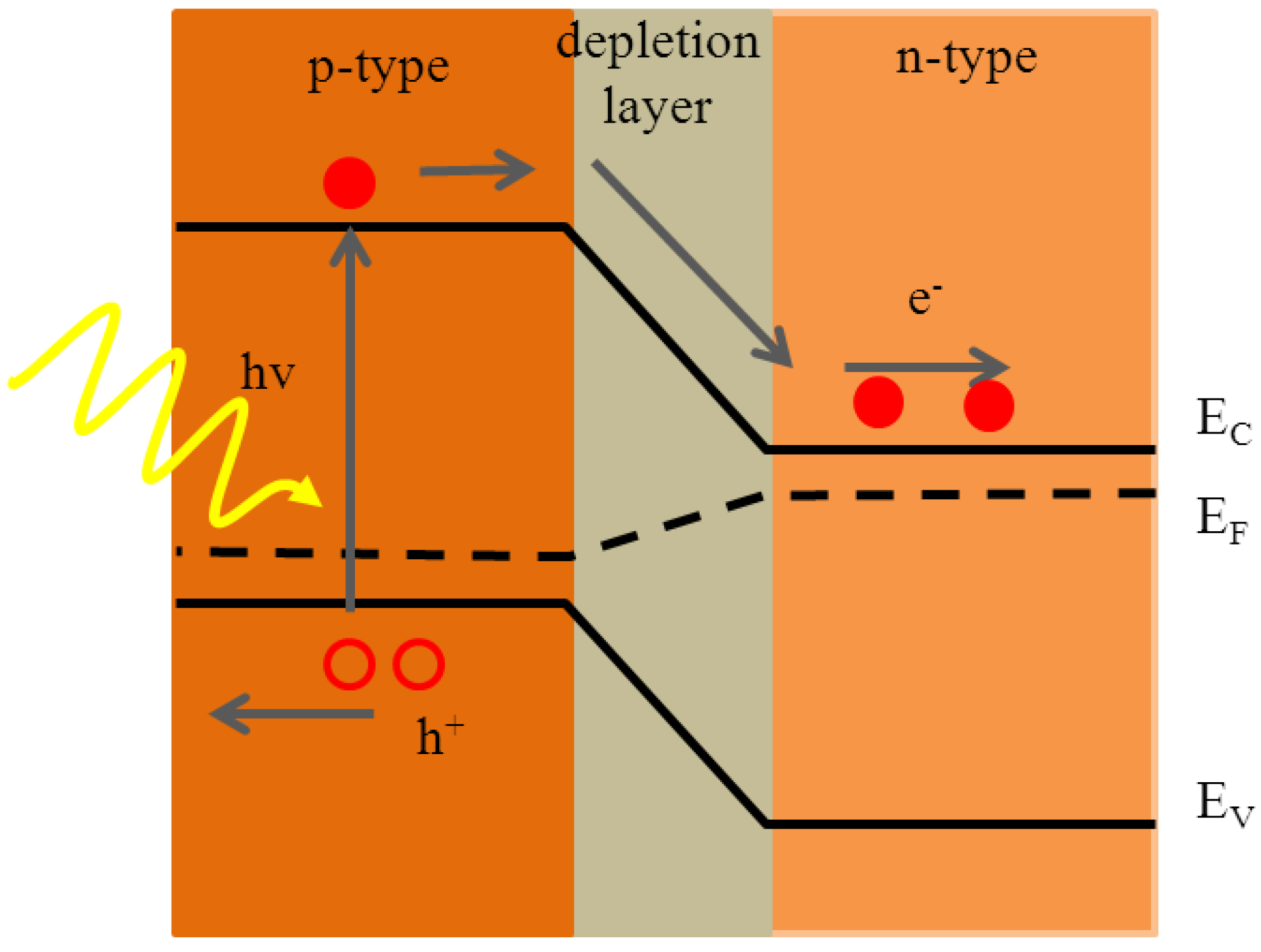
Crystalline silicon photovoltaic cells are typically made of p-n devices consisting of a junction formed around the interface of two semiconductors with differently charged majority carriers. In such a device, a photocurrent arises from minority carriers generated by photo-excitation of the semiconductor absorber. An electric field present at the p-n junction separates the electrons and holes such that electrons flow to the n-doped layer and holes to the p-doped material, resulting in a net current flow. A schematic of the energy levels within the device is presented in Figure 3.
The spectral response of crystalline silicon ranges from ~350 to 1100 nm and with PV cells with absorbers of a few hundred microns thick, efficiencies in the range of 16%–24% are achievable. The oxides of Si, Ta, Ti and Al have been used as antireflection and/or passivation layers in crystalline Si PV cells. For good antireflection at the silicon/air surface, the oxides are required to have a refractive index of around two.
Figure 3.
Schematic of the energy band diagram of an illuminated pn junction diode. EC, EF and EV are the energy levels of the conduction band minimum, the Fermi level and the valence band maximum.
Figure 3.
Schematic of the energy band diagram of an illuminated pn junction diode. EC, EF and EV are the energy levels of the conduction band minimum, the Fermi level and the valence band maximum.

Passivation of c-Si PV cells is an unavoidable process step because the discontinuity of the crystal lattice at the surface, coupled with dopants segregating at the surface and bulk defects, promotes recombination of minority carriers that reach the surface of the silicon and thus reduce PCE [64]. The passivation of silicon by dielectric oxides takes place by creation of a fixed field of the same charge as the minority carriers in the silicon to repel and thus shield them from participating in recombination at the interface [65]. For n-type silicon PV cells, where the electron-hole pairs are generated close to the front of the device, a low front surface recombination is required so that minority carriers from the entire PV cell length can reach the rear emitter. The formation of thermal SiOx at a c-Si wafer surface induces a positive fixed charge at the interface which prevents holes from approaching the surface. Since holes are the minority carrier in n-type material, field effect passivation of SiOx is suitable for both highly and lightly doped n-type c-Si but only for lightly doped p-type c-Si [65]. On the other hand, an Al2O3 passivating layer can be used to accumulate a highly negative fixed charge near the interface with p-type c-Si and prevent electrons (minority carriers in p-type material) from approaching the surface and thus reduce recombination [43,44]. Ultra-thin Al2O3 passivation layers inserted between the aluminium back contact and the p-type Si emitter as well as between the aluminium contact grid and the n type Si emitter caused an improvement in the photo-conversion efficiency of a passivated and emitter and rear cell (PERC) from 21.1% to 21.7% [66].
However, for silicon wafer PV cells, SiO2 does not provide an optimum antireflection because of the big difference in refractive indices and is thus less competitive than SiN grown by PECVD which can provide both passivation and antireflection functions, simultaneously [65,67]. Nevertheless, almost all passivation schemes in silicon PV cells require the insertion of a thin SiOx layer between the n type silicon layer and the other passivating material [66,68].
Additionally thermally grown SiOx is used as a diffusion mask for common dopants of silicon such as boron, phosphorous, arsenic and antimony, and has long been used as a mask for spatially selective impurity doping on c-Si wafers [69]. TiOx has also been investigated as a phosphorus blocking barrier during the POCl3 treatment to form a selective emitter in buried contact silicon PV cells [70].
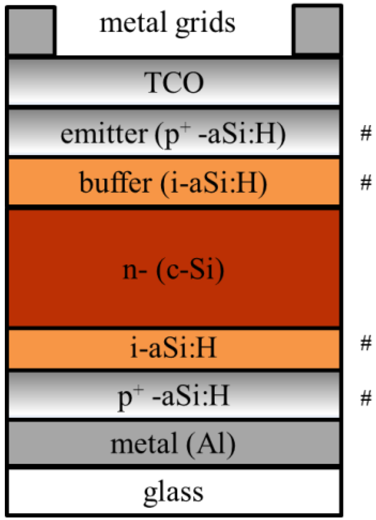
The heterojunction with an intrinsic thin layer (HIT) cell is a special type of silicon wafer PV cell whereby the p-n junction is realized by the deposition of intrinsic-doped a-Si and p-type a-Si layers on an n-type c-Si wafer using PECVD [71]. On the rear side, intrinsic-doped a-Si and n-type a-Si layers form the back surface field (BSF). TCO grown by sputtering at the front and the back of the PV cells forms the electrodes and metal grids are provided to improve current collection. The TCO at the front side of the PV cell also acts as an anti-reflection coating. The layer stack of a typical HIT solar cell is illustrated in Figure 4.
Figure 4.
Schematic of the layer stack in a heterojunction with thin intrinsic layer (HIT) silicon PV cell. The hash (#) symbols indicate layers that could be replaced by oxide films as discussed in the main text.
Figure 4.
Schematic of the layer stack in a heterojunction with thin intrinsic layer (HIT) silicon PV cell. The hash (#) symbols indicate layers that could be replaced by oxide films as discussed in the main text.

The present record efficiency on this type of PV cell is 24.7% which is quite close to the record for conventional Si wafer cells and is technologically important because all processes are done at low temperatures and on thin wafers of about 100 µm thick [72]. Since amorphous silicon (a-Si:H) strongly absorbs blue photons, silicon sub-oxides have been explored to replace it in HIT cells. Recent investigations include replacement of the amorphous silicon (a-Si:H) emitter with doped amorphous hydrogenated silicon oxide a-SiOx:H and doped hydrogenated microcrystalline silicon oxide (μc-SiOx:H) [73,74]. On the other hand, doped amorphous hydrogenated silicon oxide a-SiOx:H has been used as an alternative to a-Si:H as a passivation layer [75]. ZnO:Al has also been used as a conductive window layer in heterojunction PV cells based on n-type and p-type crystalline germanium wafers [76]. Amorphous InGa2ZnO has been applied as the n-layer in a p-n hetero-junction on p-type wafer PV cells [55].
5.2. Polycrystalline Silicon Thin Film PV Cells on Glass
Due to the high cost of wafer fabrication, there is an increasing interest in the growth of polycrystalline silicon onto foreign substrates. Typically, the silicon thin films are grown using electron beam evaporation [77] or chemical vapour deposition [78] and are thereafter crystallised to form polycrystalline films. In solid phase crystallisation, the silicon is heated for several hours at about 600 °C [77] and in some cases; metal thin layers such as aluminium are used to induce crystallisation in silicon seed layers which aid epitaxial growth of the subsequent “bulk” silicon layer [79]. In another technique known as liquid phase crystallisation, the silicon is melted using either a high power laser [80] or electron beam [78] and then crystallises as it cools. A TCO such as ZnO:Al at the front of the cell may be used as a front electrode and as antireflection coating [78]. An intermediate layer between the glass and silicon is required to block the diffusion of contaminants such as boron, sodium and iron from the glass into the silicon, to supply the doping ions to the silicon, to promote adhesion between the glass substrate and the silicon as well as in the substrate configuration and to act as an antireflection layer [80]. The intermediate layer consists of either SiOx, SiC, SiNx, or a stack consisting of one or two of these materials but the presence of SiOx at the interface with polysilicon is mandatory for high values of photo-voltage and efficiency [80]. Efficiencies up to 11.7% have been reported on a laboratory scale for laser crystallised polysilicon PV cells [80]. The main challenges for this technology are the complicated contacting scheme.
5.3. Ternary Compound Semiconductor PV Cells
Several ternary compounds are known to be photo-active in a broad spectral range and these include chalcogenides such as Cu(In,Ga)(Se,S)2 also referred to as CIGS(Se), CdTe, CuZnSn(Se,S) and the so-called III-Vs such as GaAs, InP, GaInP and GaInAs. In the following, discussion is devoted mainly to the chalcogenides which find more wide spread application and are less costly to process than the III-Vs.
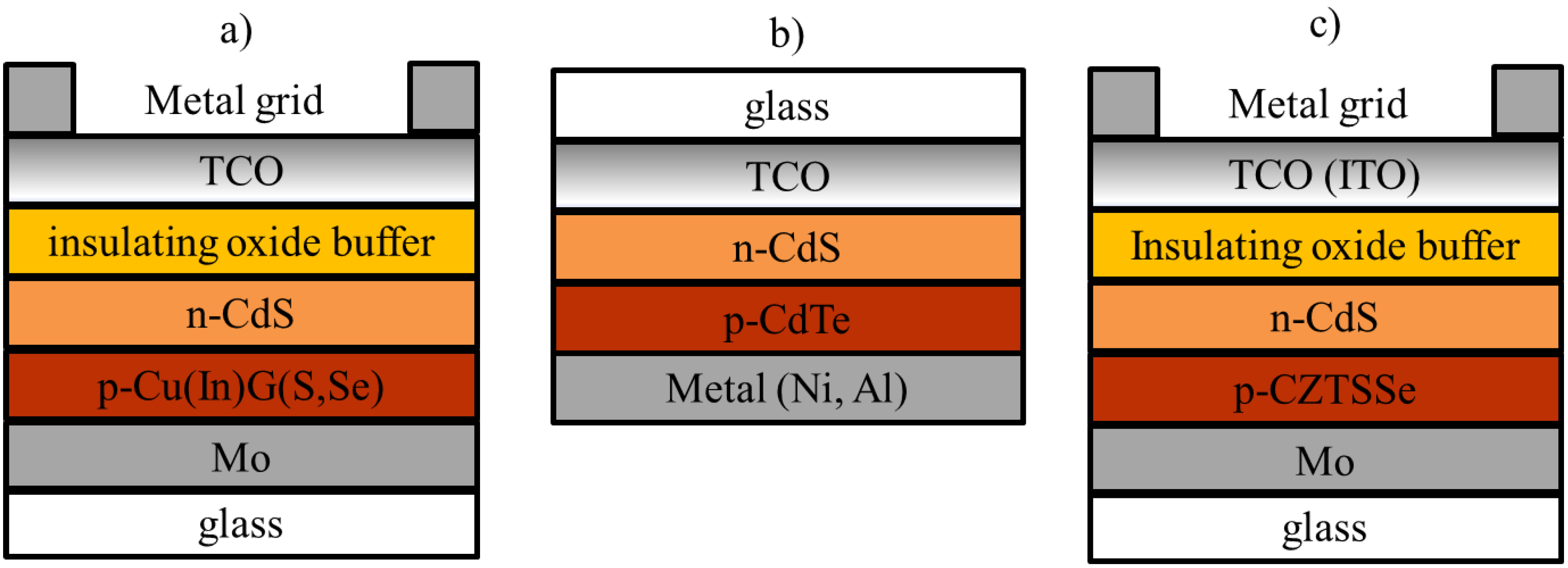
Cu(In,Ga) (Se,S)2, also known as CIGS, PV cells exhibit the highest efficiency of single p/n junction thin film PV cell made out of reasonably low cost semiconductors [81,82]. The PV cells are made up of a hetero-junction formed by p-type Cu(In,Ga) (Se,S)2 absorber joined with an n-type layer as shown in the schematic in Figure 5a.
Figure 5.
Layer stack for (a) a typical CIGS(Se) PV cell in the substrate configuration; (b) a CdTe PV cell; and (c) a CZTSSe PV cell. The direction of illumination is from the top downwards.
Figure 5.
Layer stack for (a) a typical CIGS(Se) PV cell in the substrate configuration; (b) a CdTe PV cell; and (c) a CZTSSe PV cell. The direction of illumination is from the top downwards.

The n-type layer has a dual role of generating the depletion region at the junction and of acting as the buffer layer. This buffer layer prevents shunting at the n-type TCO/p-type absorber interface. However, the conduction band minimum (CBM) of the buffer should be close to or higher than that of the CIGS to supress the majority carrier recombination at the buffer/CIGS interface in order to maintain a high photovoltage in the device [83]. ZnO and Zn1−xMgxO [83,84], Zn(O,S) [85] and In(O,S,H) [86] have been used as buffer layers to replace CdS to alleviate toxicity concerns and to minimise optical losses of blue light in the window layer. Additionally, the TCO materials, ZnO(Al,Ga) [81,85] and ITO [83] which act as the window layer and as an electrical contact at the side of illumination, are an integral part of CIGS(Se) PV cells. In this case, high conductivity and high transparency are required. An intrinsically doped ZnO [81] layer placed between the buffer and the front TCO layer is used to reduce recombination by local shunts and to reduce damage to the absorber/buffer interface during further process steps. ZnO nanorods have also been used to reduce reflection losses at the front of CIGS PV cells [87]. Zn0.85Mg0.15O has been used to completely replace the i-ZnO|CdS double layer in CIGS PV cells with only a small loss in efficiency [84]. In combination with i-ZnO, the use of ZnMgO buffer led to higher efficiency than with CdS because of improved blue light quantum efficiency [88].
For CIGS grown on metal foils, SiOx and Al2O3 have been used as barrier layers to prevent contamination of the absorber by impurities from the substrate [89,90]. The insulating oxides also act as electrical insulating layers for monolithic interconnection on metal substrates. Al2O3 coated on polymer substrates has been used to protect the subsequently grown CIGS device from ingress of moisture [91]. On the other hand, thin film alkali-silicate glass layers were grown on polymer films to supply sodium to the CIGS absorber [92].
Another type of semiconductor pn-hetero-junction PV cells with significantly high photo-conversion efficiency are CdTe based. Such PV cells consist of a glass|TCO|n-CdS|p-CdTe|high work function metal structure, as illustrated in Figure 5b, with efficiency up to 19% on a laboratory scale [93]. Since CdTe processing requires high temperatures, SnO2:F is the front contact of choice because of its high thermal stability although the nearly 10 year efficiency record was reported using CdSnO [94]. A high resistance TCO such as ZnSnO4 can be used to act as an insulating barrier such that the CdS thickness can be reduced to minimise parasitic absorption of short wavelength light [95]. Despite the concerns about the toxicity of CdTe, these PV cells have been successfully adapted to large scale production because of the simple processing.
Since indium and gallium used in Cu(In,Ga)S,Se PV cells are costly and there are concerns about the hazardous nature of Cd and the long term supply of tellurium for the CdTe, kesterite-type crystal structure, Cu2ZnSn(S1−xSex)4 (CZTSSe) PV cells have emerged as an alternative. The PV cell structure is quite similar to that of Cu(In,Ga)S,Se as shown in Figure 5c and a record efficiency value of ~11% has been achieved [96].
5.4. PIN Solar Cells
Photovoltaic devices using defect rich semiconductors such as amorphous and microcrystalline silicon or germanium are made using the so-called pin configuration. Here, a defect rich intrinsically doped semiconductor is sandwiched between a heavily doped p and n-layer. The band diagram of a typical pin PV cell as well as a sketch of the cell structure is presented in Figure 6. Photon generation and carrier absorption take place in the intrinsic-layer. The different work functions of the doped layers result in a depletion layer that stretches over the width of the absorber which prevents the recombination of electron-hole pairs in the defect rich absorber. Since the doped regions have low carrier mobility, additional highly conductive contacts are required for lateral transport of the photo-carriers.
Figure 6.
(a) Cell structure of a pin single junction PV cell in the superstrate configuration. The hash (#) symbols indicate additional layers that could be replaced by oxides. In the substrate configuration, the deposition order is reversed and light enters the cell through the n/TCO interface; (b) Schematic band diagram of a pin PV cell under normal operation.

In thin film silicon pin PV cells, oxides are used for different functionalities. Usually a SiO2 [46] or SiONx barrier layer grown between the glass and front electrode is used as an anti-reflection coating and as a barrier to sodium diffusion from the soda lime glass substrate. Since the front electrode of thin film silicon pin PV cell, must be both highly conductive and transparent for visible and infra-red light, transparent conducting oxides such as ZnO:Al [97], ZnO:B [30], ZnO:Ga [29] and SnO2:F [29,46] are used for this purpose. Additionally, the surface texture achieved on these front electrodes plays a crucial role in light management by enhancing photo-current generation and thus increasing the overall PCE [29,30,46,97]. At the rear of the PV cell, a dielectric layer is required to increase the reflectivity of the metal reflector and to prevent the diffusion of metal ions from the back reflector into the silicon [98,99]. ZnO:Al, ZnO:B and ZnO:Ga are the preferred materials for the back reflector because they can be grown at low temperatures. ZnO:B [100], ZnO:Al [101,102] and SnO2:F grown by LPCVD, magnetron sputtering and APCVD, respectively, are well established TCOs for thin film silicon PV modules fabricated on an industrial scale.
In certain instances, a TiOx layer is grown between the front TCO and the first doped layer of the thin film silicon pin PV cell to reduce reflection losses by providing a less abrupt change in refractive index at this interface [15,103]. The presence of intrinsic SiOx on a TCO substrate is reported to promote a higher nucleation density of µc-Si:H than on a-Si:H or ZnO [104,105]. When an ultra-thin undoped SiOx buffer is inserted between the p- and i-layer of a µc-Si:H PV cells, a roughly 1% absolute efficiency gain to 8.5% can be achieved [105]. The enhanced efficiency has been attributed to better antireflection at the front of the cell leading to a gain in photocurrent from low wavelengths and a reduction of boron contamination of the absorber which increased the VOC.
Amorphous boron doped hydrogenated silicon oxide a-SiO:H, as a p-layer was reported to improve the efficiency of single junction a-Si:H pin PV cell compared to amorphous boron doped hydrogenated silicon carbide a-Si:C:H due to increased fill factor as a result of higher photoconductivity [106]. Wide band gap n-type and p-type hydrogenated microcrystalline silicon oxide (μc-SiO:H) films can be grown by PECVD with high conductivities [107,108,109,110]. A study using electron energy loss spectroscopy (EELS) combined with transmission electron microscopy (TEM) and Rutherford backscattering on typical µc-SiO:H layers for thin film silicon revealed that this material consists of a mixed phase matrix of SiO and Si filaments with an oxygen atomic content x, between 0.4 and 0.8 [108]. Such layers have been successfully implemented on a laboratory scale in a-Si:H single junction [105], µc-Si:H single junction [105,111], amorphous-microcrystalline silicon multi-junction tandem [108,109,112] and in a triple junction a-Si:H/a-SiGe:H/nc-Si:H [113] device to replace a-Si:H, µc-Si:H or a-SiC:H based doped layers. On an industrially, relevant scale, µc-SiOx:H layers have been used for a-Si:H/µc-Si:H modules [102]. At the front of the PV cell, doped a-SiOx or µc-Si:OH, layers enhance the blue light quantum efficiency by reducing parasitic optical losses compared to non-oxide materials and thus increase the overall device [114]. Additionally, a resistive µc-Si:OH layer between the n-layer and the back contact resulted in increased VOC and PCE via shunt quenching for a-Si:H PV cells grown on rough substrates [115].
In recent developments, there have been investigations on p-type metal conductors such as WOx [20] and MoO3 [18] as replacements for the p-type silicon alloys in a-Si:H single junction PV cells with reasonable PV cell performance.
High efficiency in multi-junction PV cells requires that at the maximum power point all the sub-cells produce the same photocurrent, by what is termed current matching. Intermediate reflectors can be placed between adjacent sub-cells so that unused high energy photons are reflected back into the preceding wider band gap absorber while transmitting the longer wavelength light to the narrower band gap absorber below, increasing both the effective current density in multi-junction PV and the overall efficiency. Originally, ZnO was used as an intermediate reflector in tandem PV cells [116]. However, doped Si:O:H layers have been used to allow growth of the intermediate reflecting layers without a vacuum break between the two sub-cells [15,110,112,117]. The current thin film silicon PV cell stabilised efficiency of 13.4% was reported on a a-Si:H|µc-Si:H|µc-Si:H stack employing an n-type µc-SiO:H intermediate reflectors [117].
The n- and p-layer of the adjacent sub-cells in a monolithically connected multi-junction PV cell form an n-p diode that is reverse biased during forward bias operation under illumination. However, the contact between the sub-cells must be ohmic for efficient flow of charge carriers. For example, in pin/pin tandem cells, the electrons from the top cell must recombine with holes from the bottom-cell; in order to avoid charge accumulation that would block the transfer of photo-generated carriers out of the tandem cell terminals. Usually a highly doped layer is inserted between the p- and n-layer of adjacent sub-cells to facilitate charge transport by recombination of oppositely charged carriers arriving from the sub-cells. The use of an ultra-thin SiOx layer at this interface has been shown to promote recombination and thus increase the efficiency of a-Si:H|a-Si:H [118,119] and a-Si:H|µc-Si:H [112] tandem PV cells.
Lastly, a group of researchers in Japan have investigated the use of wideband gap a-SiO:H as an absorber pin PV cell, as with this material an open circuit voltage exceeding 1.0 V is possible. Single junction pin PV cells using a-SiO:H films as absorbers resulted in an efficiency of 5.5% with an open circuit voltage of 1.04 V [120]. Additionally, the use of a-SiO:H instead of a-Si:H, as a wide band gap absorber in a-Si:H [121] and µc-Si:H [122] based double junction pin PV cells, has been reported to reduce the temperature coefficient of such devices. Although this material with an oxygen content of 2%–4% a-SiO:H may technically not be considered an oxide, it offers a glimpse of the scope for further insight into the development of wide band gap top cells in multi-junction devices and single junction PV cells with high terminal voltage.
5.5. Dye sensitized Solar Cells
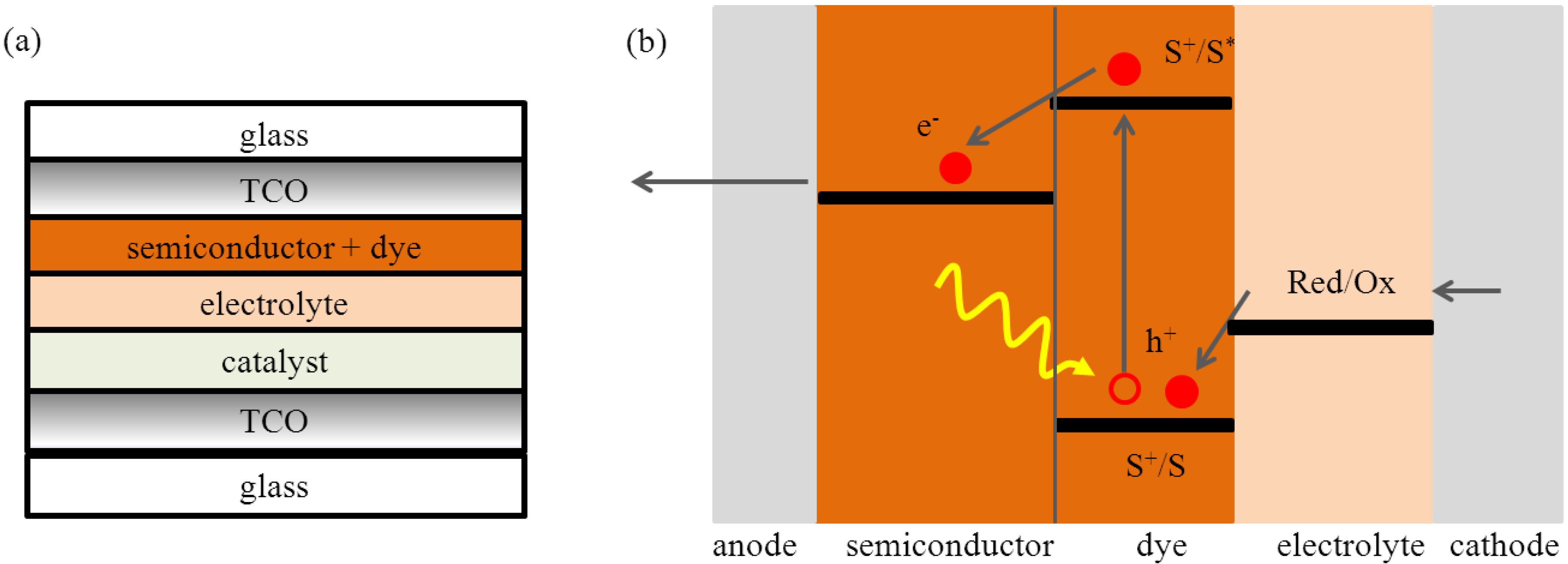
Intrinsically doped TiO2 [123,124] is widely used in dye sensitised solar cells (DSSC) although other wide band gap metal oxides such as ZnO and SnO2 have also been investigated [125]. The schematic of a single junction DSSC and a sketch showing the band levels during normal operation are shown in Figure 7.
Figure 7.
(a) Cell structure of a pin dye sensitised solar cell (DSSC); (b) Schematic band diagram of a DSSC under normal operation. S, S+ and S* stand for neutral, ionised and excited sensitizer, respectively.
Figure 7.
(a) Cell structure of a pin dye sensitised solar cell (DSSC); (b) Schematic band diagram of a DSSC under normal operation. S, S+ and S* stand for neutral, ionised and excited sensitizer, respectively.

Typically, a mesoporous antase phase TiO2 film is deposited by screen printing on a conducting (usually FTO or ITO coated) glass sheet that serves as current collector. The TiO2 is covered with a charge transfer dye also known as the sensitizer which under illumination injects an electron into the conduction band of the TiO2. The photogenerated charges diffuse to the back and front contact, to generate an electric current, i.e., the electron is transferred to the TCO layer whilst the corresponding hole is transferred to the counter electrode consisting of a catalyst such as platinum or carbon. The electronic state of the dye is restored by electron donation from an electrolyte containing a redox couple, typically iodide/tri-iodide [123]. The tri-iodide gains an electron by completion of the external current flow then passes this on to the iodide, thus the system is quasi-self-sustaining. The photovoltage obtained is related to the difference in the Fermi levels of the electrons in the semiconductor and of the redox potential of the electrolyte. Using this configuration, a PCE of 11.1% has been demonstrated [124]. However, problems with sealing make the lifetime of the device relatively short compared to all inorganic PV cells. A blocking layer is required to slow the recombination of injected electrons with the oxidised redox couple and/or the oxidised sensitizer (normally, dye molecules) and thus maintain a high open circuit voltage. Since the blocking layer forms a potential barrier between the anode and the electrolyte, a wide band gap or insulating material may fulfil this purpose. Usually an ultra-thin compact TiO2 is used as a blocking layer however, it is expected that a nominally insulating oxide with a higher dielectric constant would perform better. Palomares et al. compared the use of ultra-thin Al2O3, ZrO2 and SiO2 as ultra-thin blocking layers and all cells using these materials showed equal or better performance than with a TiO2 blocking layer, with the best performance for Al2O3 [126]. Other oxides used as blocking layers for DSSC include Nb2O5 [127] and MgO [128].
ZnO has become attractive as a semiconductor for DSSC since it can be easily fabricated with various nanostructures at low temperatures [129] and has a higher electron mobility than that of TiO2. However, ZnO is less chemically stable than TiO2 and may necessitate an additional layer for protection from the electrolyte. The possibility of using p-type semiconductors as opposed to n-type TiO2 for DSSC has been explored where, under illumination, electrons are transferred from the valence band of the semiconductor into the HOMO of the sensitizer and then onto the oxidised species of the electrolyte. Examples of p-type semiconductors used for DSSC include NiO [130,131] and CuAlO2 [132]. New directions in DSSC research include the development of tandem n-DSSC|p-DSSC devices which are expected to have enhanced efficiency since the VOC depends only on the offset between the p-layer VBM and the n-layer CBM rather than on the redox potential of the electrolyte. The current efficiency record of 15% at 96.4 mW·cm−2 irradiation level was reported for a DSSC using a perovskite pigment to sensitise the TiO2 [133].
5.6. Organic Photovoltaic Cells
The photo-active layer of an organic photovoltaic (OPV) cell consists of either a blend [134] or a bi-layer [135] of donor and acceptor organic molecules sandwiched between two electrodes. The most commonly used organic molecules are poly(3-hexylthiophene) (P3HT) as the electron donor and [6,6]-phenyl C61-butyric acid methyl ester (PCBM) as the electron acceptor. An energy level offset exists between the lowest unoccupied molecular orbital (LUMO) of the acceptor and the conduction band edge of the acceptor material or between the highest occupied molecular orbital (HOMO) of the donor and the valence band edge of the acceptor material. When photons with sufficient energy are incident on the photoactive layer, an exciton, consisting of a coulombically bound electron-hole pair, is formed. The energy level offset at the interface between the donor and the acceptor material is used to dissociate the exciton so as to free the charge carriers [136]. The energy level offset between the donor and acceptor material also appears to determine the VOC device [136] but other researchers have contradicted this result as discussed in a separate review [137]. If the exciton was generated in the donor/acceptor material, an electron/hole separated at the interface can be transferred to the acceptor/donor and then onto the cathode/anode for transport outside the cell.
During hole injection, an electron is transferred from the organic HOMO to the CB of the metal oxide while for hole-extraction, electrons in the CB of the metal-oxide recombine with photo-generated holes at the interface with the organic “absorber”. Since the optimum HOMO level of organic molecule donors for the right balance between high JSC and high VOC, is relatively high at between −5.2 and −5.6 eV, this has serious consequences for the choice of electrode materials used [136]. A high work function material is required at the anode so that the Fermi level EF matches that of the HOMO of the donor. High work function metals are unsuitable for this purpose because they readily supply electrons into the donor which causes a drop in the built in potential. Poly (3,4-ethlendioxythiopene):poly(styrenesulfonate) (PEDOT:PSS), a p-type polymer, has in the past been used as a hole extraction layer/anode for high efficiency OPV. However, since PEDOT:PSS is acidic, it shortens the lifetime of the device by corroding the TCO electrode. Transition metal oxides which have a high work function, a wide band gap, are relatively chemically stable and can be prepared with low cost processing techniques have been tested as HELs with promising results [138]. Prolonged device lifetime at similar levels of initial efficiency has been reported for transition metal oxides e.g., NiO, V2O5, MoO3 and WO3 [17].
On the other hand, since the organic acceptor has a high electron affinity, a material with a low work function that is equal to or less than the LUMO of the acceptor, is required at the cathode to form an ohmic contact for efficient extraction of electrons and to maintain a high open circuit voltage. Additionally, the electron extracting layer (EEL) must have a high electron mobility and be able block holes from crossing the active layer|cathode interface to prevent recombination of the electrons before extraction. The EEL should also act as a chemical barrier to prevent reaction between the organic active layer and the metal electrode. High optical transparency of the EEL in the wavelength range where the organic absorber is active is desirable especially for inverted configuration (which shall be discussed shortly). Low work function metal oxides such as TiO2 [139] and ZnO [140] are popular materials for EEL as they fulfil most of the above requirements and provide better device stability than metallic or organic based electron extraction layers. The chemical conditions that make a given metal oxide suitable for use in an OPV either as a hole or electron injector have been reviewed in another article [141].
There are two types of configurations for organic based PV cells namely, the conventional and the inverted design. In the conventional design, the hole extracting layer HEL is illuminated before the BHJ and thus the TCO acts as an anode while in the inverted design the order of layers is reversed such that the TCO acts as the cathode [142] as shown in Figure 8.
Figure 8.
Layout of (a) a conventional and (b) an inverted organic photovoltaic device (OPV); (c) Schematic of the energy level diagram showing the working principle of a conventional single junction OPV device with photogeneration occurring in the electron donor. Note that in the conventional layout, a low work function (WF) metal oxide may also be inserted between the BHJ and the low WF metal.

Generally, the PCE of OPV devices is partially limited because carrier separation can only occur where photo-generation is within the excitonic diffusion length of the interface. The highest OPV cell efficiency to date, was ~11% for a glass|ITO|ZnO|P3HT:ICBA|PEDOT:PSS|ZnO|PDTP-DFBT:PCBM |MoO3|Ag stack [143].
5.7. Concentrator Photovoltaic Devices
In concentrator photovoltaic (PV) cells, the incident light is focused onto a small highly efficient PV cell using optical lenses or mirrors such that concentrated irradiation intensity is several hundred times higher than the incident value [143]. The advantage of this type of PV cell is that the material costs can be reduced by using a small active cell area and that less space is required compared to conventional (non-concentrator) PV cells, to achieve a given power output. The main disadvantage is that a sun tracking system is usually mandatory to maintain high efficiency throughout the day. The absorber materials usually consist of multi-junctions on a silicon or germanium wafer. The highest efficiency to date is for a quadruple junction device based on III-V compound semiconductors with a value of 44.7% for a concentration of 297% Suns [7]. For concentration exceeding 10 Suns, cooling is required to reduce the dark current component so as to maintain high values of voltage. To this end passive cooling schemes using high thermal conductivity ceramics or active cooling are used. Beryllium oxide, though toxic, and aluminium oxide, both with high thermoconductivity as well as high electrical resistance, are used in cooling stacks to remove heat dissipated in CPV devices [144].
6. Emergent PV Concepts Benefiting from the Use of Oxides
As part of the effort to make PV technology more efficient and competitive among other energy sources, the device architecture of well-known PV materials is being modified and new PV concepts are emerging, all of which benefit from the improved understanding of oxide materials. Additionally, simple and ternary oxides that were hitherto irrelevant for PV are being continuously added to the palate of materials used to explore and/push the efficiency boundaries in photovoltaic cells. While some of these materials have only functional purposes i.e. are not photoactive, others are used to provide the junction and even generate the photo-carriers.
6.1. Semi-Transparent PV Cells
Transparent PV cells are of interest for building integrated photovoltaic systems where they serve the dual purpose of fenestration and energy generation. For this purpose, transparent conducting oxides are the electrodes of choice at both the front and rear of the PV cell because of their visible wavelength transparency. Different types of PV cells have in the past been investigated for transparent PV namely, OPV [139,145,146], thin film silicon [147] and CIGS [148].
6.2. Bifacial PV Cells
Bifacial PV cells are designed to make use of both rear and front side reflection and thus require the use of transparent oxides as electrodes. Bifacial PV cells have been reported using CIGS [148,149], dye sensitized solar cells [150] and CdTe [151]. It is to be noted that bifacial cells may not necessarily be semi-transparent depending on the thickness and band gap of the absorber layer.
6.3. Mechanically Stacked PV Cells
Mechanically stacked PV cells offer the benefits of multi-band gap PV cells while avoiding problems associated with growing the subsequent sub-cell directly on the existing one. As the top PV cell must transmit as much of the unused light to the bottom cell, metal electrodes are undesirable and thus transparent conductors play an important role as the contacts. Some examples of mechanically stacked PV cells include CGS|CIGS [152], TiO2 DSSC|CIGS [153]. Although ITO is a relatively “old” oxide for PV cell applications, new device concepts are still being developed using this material. For instance, in Japan, mechanically stacked multi-junction Si|Si and, InGaP|GaAs on Ge, PV cells, using an adhesive combined with ITO particles, have been successfully demonstrated [154].
6.4. Oxide Nanosized Materials for PV
The use of nano-sized materials in PV cells has been fashionable since the early 2000s [137] after the demonstration of a high efficiency DSSC using TiO2 nano-particles [123]. Naturally, oxides being simple to prepare in nano-particle size, play an important role in the drive to achieve high efficiency in “nano-based” PV devices. Al2O3 nanoparticles have been used to improve light in coupling in silicon nanowire PV cells to increase the quantum efficiency [155]. ZnO nanowires have been used for DSSC [156]. The field of nano-sized materials in PV is too wide to discuss on its own here and overlaps several other technologies such as quantum dots, hybrid organic/inorganic PV cells of which, some examples are presented.
6.5. Photonic Crystals for PV
If two media of differing dielectric constant are adjacent to each other, light will propagate slower in the medium of higher dielectric constant. If the two media are spatially arranged, then a spatial periodicity in their dielectric constants exists and this could be in 1-, 2- or 3-dimensions. Such materials are known as photonic crystals PCs. Due to the periodicity of the dielectric constants, interferences will exist that prevent specific frequencies from propagating through the PC giving rise to forbidden and allowed bands. If a photon of a wavelength comparable to the periodicity of the lattice of the photonic crystal is reflected back it is thus blocked from passing through the PC. Recently, photonic crystals have been integrated into different PV devices to improve the light management. A thin film silicon tandem PV cell using a photonic crystal consisting of inverted ZnO opals as an intermediate reflecting layer has been experimentally demonstrated, although efficiency values were not provided [157]. Photonic crystals, whereby the optical contrast is realised between a patterned BHJ blend (high refractive index) and ZnO (low refractive index), have also been used to increase the absorption in organic PV cells compared to flat devices [158]. Photonic crystals consisting of inverse opal TiO2 have been used to increase the absorption and thus photogeneration in dye sensitized solar cells [159].
6.6. Photovoltaic Integrated Devices for Stand-Alone Functionality
PV integrated optoelectronic devices are attractive because the omission of external wire connections minimises resistance losses, makes the device compact and simplifies the fabrication. At least one of the devices must be semitransparent to allow transmission of photons to the adjacent one.
In hybrid photovoltaic-photoelectrochemical (PEC) devices part of the incident photons are used to photocatalytically split water into oxygen and hydrogen and the rest to generate a photovoltage. The PEC device consists of a photocatalyst, at the anode, and a cathode separated by an aqueous electrolyte [160,161]. When light of high enough energy is incident on the photoanode, electron-hole pairs are generated. The photogenerated holes oxidise water at the surface of the photocatalyst releasing oxygen gas and hydrogen ions. The electrons are transferred to the cathode via an external circuit, where they reduce the H+ ions to give hydrogen. Since anodic electrode materials with a high enough band gap to provide a voltage higher than the dissociation voltage of water are rare, the use of bias potential supplied by an integrated photovoltaic cell is attractive. The sketch in Figure 9 shows the layout of the monolithically connected PV/PEC cell and the energy level diagram of such a device.
Figure 9.
(a) Layer stack and (b) energy level diagram of a photovoltaic-photoelectrochemical (PV-PEC) hybrid device.
Figure 9.
(a) Layer stack and (b) energy level diagram of a photovoltaic-photoelectrochemical (PV-PEC) hybrid device.

Ideally, the PV cell should be capable of delivering a high enough voltage level to exceed the dissociation voltage of water (1.23 V) and to compensate voltage losses along the various interfaces of the device. The PV cell creates a photovoltage and current as a result of incident light transmitted through the transparent PEC device and the operating point of the hybrid device is determined by the intersection of the J-V curves of the PV and the PEC device [160]. The use of a metal oxide photoanode allows the use of a device consisting of a monolithically grown PEC and PV cell layer stack immersed in the electrolyte since when well-chosen; the metal oxide provides chemical protection to the rest of the device [160]. Multi-junction thin film silicon PV cells are an attractive partner for PV/PEC cells because the amorphous cell already provides ~900 mV. First devices using a-Si/a-Si double junctions [162] and crystalline Si|a-Si|GaP in hybrid PV PEC devices have been demonstrated [163].
Another concept is the stand-alone PV powered electrochromic window (ECW) which combines a PV cell with a fenestration device that reversibly changes its colour/transparency depending on the voltage applied to its terminals. Several such devices have been described in the literature [164,165]. Since it is desired that the ECW darkens under strong sunlight, increasing the irradiation intensity on the PV cell would increase its current output which would in turn increase the voltage bias across the ECW, thus reducing its transparency appropriately to achieve a shading effect. Under low sunlight intensity, the PV device is inactive and the ECW is highly transparent allowing maximum light transmission into the building. Clearly, metal oxides used instead of metal films as electrodes, play an important role in ensuring that the whole device is semi-transparent in the bleached state.
6.7. Luminescent Spectral Converters
A significant part of the sunlight incident on contemporary PV cells cannot be used for photogeneration. Photons with energy less than the band gap energy are transmitted or reflected out of the PV cell while those higher than the band gap energy are wasted via thermalisation of carriers as already summarised in Figure 1. Luminescent spectral up- and down-converters are materials that absorb photons of a certain energy level and via electron transitions, re-emit them at higher or lower energy levels, respectively making them attractive PV cell components in the bid to enhance the photoconversion efficiencies.
The oxides of rare earth RE and lanthanide Ln metals that is, Sc, Y and La in group 3 and the lanthanides, exhibit photoluminescence. The electronic structure of their oxides consists of a valence band of filled O 2p states, a band gap of the order of 5.5 eV, a main conduction band of empty Ln 5d states, and filled and empty Ln 4f states which can lie in these bands or in the main band gap [19]. The partially filled 4f electron shell is shielded by filled 5s2 and 5p6 shells making the luminescence behavior largely independent of the surrounding conditions such as crystalline structure or presence of a foreign host material [166]. Although the RE- and Ln-oxides are wide band materials, photoabsorption caused by local excitations within the 4f electron shell lead to optical transitions that appear as sharp emission spectra.
In up-conversion, the up-converter film may be placed behind the PV cell where it absorbs the transmitted long wavelength photons. Ideally, the absorption of two sub-band gap photons by the up-converter should lead to the emission of one photon with energy for which the PV absorber material has the highest spectral response [167]. The up-converter should also have an energy band gap equal to that of the PV absorber. La2MO2O9: Yb, R (R = Er, Ho) films screen printed on top of silicon wafer PV cells have been shown to increase the overall cell efficiency compared to bare cells [168]. In this case, La2Mo2O9 was the host material while Yb3+ was the sensitizer which triggers the process by absorbing low energy photons then re-emits the photons at another energy level to the activators i.e., Er or Ho where via a further luminescence process, higher energy photons are emitted for absorption by the PV cell absorber for photoconversion.
On the other hand with down conversion, the down-converter film should absorb one photon and re-emit two photons both of which with an energy at which the PV absorber has a high spectral response [169]. The down-converter should ideally have an energy band gap double as wide as that of the PV absorber and should possess impurity levels at the centre. Gd2O3:Eu nanocrystals dispersed in mesoporous TiO2 enhance the DSSC efficiency by excitation of Gd2O3 by UV light which transfers charge to Eu then onto the TiO2 [170]. In another configuration, through Eu3+ and Sm3+ doping, UV light absorbed by mesoporous TiO2 can be re-emitted over a relatively broad band from 550 to 750 nm [171]. The efficiency of DSSC using TiO2 doped by the lanthanides Sm3+ and Eu3+ could be enhanced compared to that of undoped TiO2 [172].
6.8. Hybrid Organic-Inorganic PV Cells
Hybrid organic-inorganic PV cells are being investigated in order to benefit from a combination of the promise of low material cost of organics and the ability to tune the band gap of inorganic materials [137]. In such devices, an inorganic material such as silicon, CdSe or a metal oxide replaces the organic electron acceptor. In one development, the neodymium oxide is combined with PCBM to form an organic-inorganic hybrid BHJ cell [173]. The absorption of photons of energy ≥2 eV significantly improved and was accompanied by an increase in the device photocurrent and photo-conversion efficiency. The increased photocurrent was attributed to charge transfer between Nd2O3 and the PCBM as proved by absorption peaks measured by transient absorption pump-probe spectroscopy, corresponding to valence- to f-band transitions in Nd2O3.
6.9. Extremely Thin Absorber ETA Solar Cells
ETA solar cells are pn heterojunction devices consisting of a nanostructured wide gap semiconductor conformally coated by a very thin p-type absorber layer [174]. The nanostructure of the pn junction increases the optical path of the light in the device thus allowing the use of a thinner absorber which improves the photocarrier collection efficiency. The ETA is preferably deposited onto the nanostructured substrate using solution based processing to ensure a close contact at the pn junction. The n-contact and absorber materials are chosen so that the band alignment allows electron flow from the absorber to the n-contact while a large valence band offset block hole transfers across this interface. Holes are transferred across the absorber/metal interface. As with other types of semiconductor PV cells, such as CIGS or CdTe based types, one electrode is normally a transparent electrode, usually a TCO film and the other, a metal. As an example, a glass|SnO2:F|TiO2|CdTe|Au device with only 170 nm of CdTe could generate a short circuit density of 8.9 mA/cm² [174] which is a third of the value of state of the art CdTe PV cells with an absorber thickness of a few microns [93].
6.10. Perovskite Absorber PV Cells
A PV device based on a schottky junction using a SrTiO3 crystal as the absorber has been demonstrated [51]. By using perovskite PV cells based on methylammonium lead halides (CH3NH3PbX3), where X is Ch, I or Br, impressive PV cell performance has been achieved by several groups. Efficiency values of up to 10.9% can be achieved with a glass|SnO2:F|compact n-type TiO2|(CH3NH3PbI2Cl) + mesoporous TiO2 or Al2O3|p-type 2,29,7,79-tetrakis-(N,N-di-p-methoxyphenylamine) 9,99-spirobifluorene (spiro-OMeTAD)|metal device stack [175]. Recently, an even higher efficiency of 15.4% was obtained by using a similar structure using a physical vapour deposited (CH3NH3PbX3) that omitted the mesoporous oxide but retained the compact TiO2 as an electron selective layer [176].
6.11. “New” Single Cation Oxides for PV
Lead oxide has also been investigated as an absorber material in PV cells although the efficiency is still too low [40]. Graphene oxide (GO) consists of hexagonal ring networks of sp2 hybridized carbon atoms of graphene whose stacked planes are randomly disrupted by sp3 hybridized carbon atoms covalently bonded to oxygen functional groups [177]. The conductivity of GO can be varied from a semi-metallic through semi-conductor to insulating by increasing the fraction of sp3 C-O bonds [177]. Moreover, GO films that are a few nm thick behave like a conducting transparent oxide making it an interesting material for opto-electronic applications. GO has been employed as a hole [178,179] and electron [179] transporting layer in organic PV cells.
Anodic aluminium oxide (AAO) is made by anodising aluminium foils or thin films on a foreign substrate by electrolysis in oxalic, citric or phosphoric acid [180]. When a pattern is imprinted on the aluminíum prior to the anodization, ordered or periodic structures are formed after the anodization. Although AAO is well known, only a few exploratory studies have been directed to PV cell application. AAO can be used as an angular selective back scatterer in semi-transparent OPV [146]. Tsao et al. studied the use of AAO structures as back surface reflectors for light trapping in thin film silicon PV cells but did not report the achievable PCE values [180]. AAO has also been successfully demonstrated as suitable for large area formation of antireflective coatings for PV cells [181].
6.12. Ferro Electric Photovoltaics
Unlike conventional photovoltaics, the open circuit voltage produced by ferroelectric photoactive materials exceeds their band gap due to a polarisation related charge separation mechanism. This effect was observed, in the 1970s, for several materials including LiNbO3 [182]. Recently, more studies have shown that the value of the above-band gap photovoltage of ferroelectric BiFeO3 can be tuned by varying the number of nanometre scale domain walls with alternating polarity, and additionally, by varying the applied electrical field [183]. However, the efficiency of such devices based on ferroelectric materials such as BiFeO3 and Pb(Zr,Ti)O3 (PZT) remains very low due to the low fill factor and Jsc [184,185,186] PV cells using KNbO3, another perovskite ferroelectric material, as the absorber have been reported [53].
6.13. All Oxide PV
As a result of the (re)emergence of oxide semiconductors with band gaps low enough to absorb light in the VIS-NIR wavelength spectrum, the concept of all-oxide photovoltaics has become an interesting research topic [187]. The oldest “all oxide” PV cell technology makes use of a pn junction consisting of Cu2O and an n-type transparent conductor with efficiencies ranging from 0.4% to 3.8% as reviewed recently [21]. Since then, a current record efficiency of 5.38% has been achieved by including a pulsed laser deposited Ga2O3 with a work function of 5.08 eV which lies close to the electron affinity of Cu2O in an Al-doped ZnO|non-doped Ga2O3|Cu2O hetero-junction PV cell [23].
A more recent development in “all oxide” PV makes the use of layered oxide heterostructures consisting of insulating oxides of differing band gap that become photo-active when they form a heterojunction, as absorber materials [52]. This works on the principle that above a critical thickness, the interface of these insulating materials becomes conductive, for example, a concept consisting of a gap-graded oxide heterostructure cell made up of several LaVO3|SrTiO3 double layers which have an effective band gap of 1.1eV [52]. The n- and p-type regions of the PV device exist at the (TiO2|[LaO]+) and the (SrO|[VO2]−) interfaces, respectively. Light incident on the device generates photocarriers in the LaVO3 layers which are then separated by the built in voltage that develops between the n- and p-regions.
6.14. Quantum Effect Photovoltaic Devices
Quantum effect photovoltaics use the quantum effect to vary the spectral response of the absorber layer by using quantum dots (QD) or quantum wells (QW). In quantum dot (QD) photovoltaic devices, the band gap and thus spectral response of the photoactive layer is varied by tuning the quantum size of the material rather than varying the material composition as is done for conventional photovoltaics. When the diameter of a particle is reduced below the characteristic dimensions of the electron and hole wave-function of the host material, its energy levels are shifted into the bands of the bulk medium thus varying the width of the band gap. Generally, for PV applications, the p-type QD absorber is embedded in a host material usually a wide band gap n-type oxide and functions much like the dye in DSSCs described before, with the advantage that device lifetime may be prolonged [188,189]. When photons are absorbed by the QD, an electron-hole pair is formed and the electrons are transferred into the conduction band of the semiconductor. Chalogenide based QDs as sensitizers on wide band gap semiconductor oxides including TiO2, ZnO, SnO2, Nb2O5 and Ta2O5 have been investigated for PV cell application [190,191,192]. MoO3 has been used as a large work function electrode to ensure an ohmic contact at the rear of a TiO2 cell with Pbs QDs thus achieving an efficiency of 3.5% [189].
The use of colloidal quantum dots (CQD) with an absorption band edge around 1600 nm has opened the way for infra-red photovoltaics [193]. This is an important breakthrough since nearly half of the sun’s energy lies in the near infrared wavelength region and thus in order to increase the efficiency of the current PV devices, materials that are photoactive in this energy region are vital. An efficiency value as high as 7% has been reported for a glass|SnO2:F|TiO2/ZnO|CQD|MoO3|Au|Ag device [194].
Quantum well QW solar cells consist of an intrinsic absorber layer made up of a succession of stacks consisting of a lower band gap semiconductor (well) sandwiched between two higher band gap semiconductors (barrier). The intrinsic layer is in turn sandwiched between a p-type and n-type semiconductor forming a pin junction that confines the photogenerated electrons in two rather than three dimensions as in conventional PV cells. Since the energy of the electrons inside the i-layer is lower than that of the p and n layers, the flow of charge is confined to well-defined regions. The lower band gap increases light absorption but traps the photo-generated carriers and therefore it is desirable to reduce the number of quantum wells. The efficiency of quantum well PV cells can be significantly enhanced by integration of dielectric nanoparticles such as SiO2 which scatter normally incident light into lateral propagating optically confined modes within the wave guiding multiple quantum well intrinsic layer [195]. This approach enables highly efficient photon absorption and photo current generation in the ultra-thin layers and also improves collection of photo-generated charge carriers because of the high electric field in the QW region.
7. Conclusion
Oxides are an important component of PV cells and shall continue to be so in the future. Due to the diverse applications of oxides in PV cells, only a snap shot can be made of the range of devices that have been explored. On the one hand, we have the traditional oxides for various functionalities and on the other, new oxide materials are being introduced for use in PV. While the transparent conducting oxides of indium, zinc and tin are important as electrodes in most PV cell technologies, TiO2 has become the model material for PV cells based on charge transfer to a sensitised semiconductor. The oxides of silicon and aluminium, both members of the semi-metal group, when highly insulating can be used for passivation due to their high dielectric constant. The transition metal oxides with high work functions are now routinely used for organic PV cells as electrode buffer materials to maximise the cell voltage and to prevent leakage currents. Other oxides, such as those of copper and lead have been used as absorber materials. More exotic multinary oxides such as the ferroelectric perovskites BiFeO3 and KNbO3 are used as absorbers with the promise of high cell voltage. Lanthanide host oxides and lanthanide doped oxides have been introduced as wide band spectral converters to enhance the spectral response of PV cells beyond the normal absorption band of the absorber material. Much as this review has focused on examples of applications of oxide materials where PV cell performance has been experimentally demonstrated, the contribution and importance of theoretical calculations towards these and future developments cannot be overstated.
Acknowledgements
I thank various colleagues at the Competence Centre Thin Film and Nanotechnology for Photovoltaics Berlin (PVcomB) in Helmholtz Zentrum Berlin for discussions over the past years that triggered the idea for this article.
Conflicts of Interest
The author declares no conflict of interest.
References
- Torrance, J.B.; Lacorre, P.; Asavaroengchai, C.; Metzger, R.M. Why are some oxides metallic, while most are insulating? Physica C 1991, 182, 351–364. [Google Scholar] [CrossRef]
- Chopra, K.; Major, S.; Pandya, D. Transparent conductors—A status review. Thin Solid Films 1983, 102, 1–46. [Google Scholar] [CrossRef]
- Zhai, T.; Fang, X.; Liao, M.; Xu, X.; Zeng, H.; Yoshio, B.; Golberg, D. A comprehensive review of one-dimensional metal-oxide nanostructure photodetectors. Sensors 2009, 9, 6504–6529. [Google Scholar] [CrossRef]
- Robertson, J. High dielectric constant gate oxides for metal oxide Si transistors. Rep. Prog. Phys. 2006, 69, 327–396. [Google Scholar] [CrossRef]
- Gellings, P.; Bouwmeester, H. Ion and mixed conducting oxides as catalysts. Catal. Today 1992, 12, 1–105. [Google Scholar] [CrossRef]
- Bocquet, A.; Mizokawa, T.; Morikawa, K.; Fujimori, A.; Barman, S.; Maiti, K.; Sarma, D.; Tokura, Y.; Onoda, M. Electronic structure of early 3d-transition-metal oxides by analysis of the 2p core-level photoemission spectra. Phys. Rev. B 1996, 53, 1161–1170. [Google Scholar] [CrossRef]
- World Record Solar Cell with 44.7% Efficiency. Press Release 2013; Fraunhofer-Institut für Solare Energiesysteme ISE: Freiburg im Breisgau, Germany, 23 September 2013. Available online: http://www.ise.fraunhofer.de/en/press-and-media/press-releases/presseinformationen-2013/world-record-solar-cell-with-44.7-efficiency (accessed on 17 March 2014).
- Jansen, K.; Delahoy, A. A laboratory technique for the evaluation of electrochemical transparent conductive oxide delamination from glass substrates. Thin Solid Films 2003, 423, 153–160. [Google Scholar] [CrossRef]
- Cardelli, F. Materials Handbook: A Consise Desktop Reference, 2nd ed.; Springer-Verlag: Hamburg, Germany, 2008. [Google Scholar]
- Yin, W.J.; Wei, S.H.; Al-Jassim, M.M.; Yan, Y. Prediction of the chemical trends of oxygen vacancy levels in binary metal oxides. Appl. Phys. Lett. 2011, 99, 142109:1–142109:3. [Google Scholar]
- Brewer, L. The thermodynamic properties of the oxides and their vaporisation processes. Chem. Rev. 1953, 52, 1–75. [Google Scholar] [CrossRef]
- Asahi, R.; Taga, Y.; Mannstadt, W.; Freeman, A.J. Electronic and optical properties of anatase TiO2. Phys. Rev. B 2000, 61, 7459–7465. [Google Scholar] [CrossRef]
- Gordon, R. Chemical vapour deposition of coatings on glass. J. Non-Cryst. Solids 1997, 218, 81–91. [Google Scholar] [CrossRef]
- Hitosugi, T.; Yamada, N.; Nakao, S.; Hirose, Y.; Hasegawa, T.H. Properties of TiO-based transparent conducting oxides. Phys. Stat. Solidi A 2010, 7, 1529–1537. [Google Scholar]
- Das, C.; Lambertz, A.; Huepkes, J.; Reetz, W.; Finger, F. A constructive combination of antireflection and intermediate-reflector layers for a-Si/µc-Si thin film solar cells. Appl. Phys. Lett. 2008, 92. [Google Scholar] [CrossRef]
- Ito, S.; Murakami, T.N.; Comte, P.; Liska, P.; Graetzel, C.; Nazeeruddin, M.K.; Graetzel, M. Fabrication of thin film dye sensitized solar cells with solar to electric power conversion efficiency over 10%. Thin Solid Films 2008, 516, 4613–4619. [Google Scholar] [CrossRef]
- Chen, S.; Manders, J.R.; Tsang, S.W.; So, F. Metal oxides for interface engineering in polymer solar cells. J. Mater. Chem. 2012, 22, 24202–24212. [Google Scholar] [CrossRef]
- Park, S.I.; Baik, S.J.; Im, J.S.; Fang, L.; Jeon, J.W.; Lima, K.S. Towards a high efficiency amorphous silicon solar cell using molybdenum oxide as a window layer instead of conventional p-type amorphous silicon carbide. Appl. Phys. Lett. 2011, 99. [Google Scholar] [CrossRef]
- Robertson, J. High dielectric constant oxides. Eur. Phys. J. Appl. Phys. 2004, 28, 265–291. [Google Scholar] [CrossRef]
- Fang, L.; Baik, S.J.; Lim, K.S.; Yoo, S.H.; Seo, M.S.; Kang, S.J.; Seo, J.W. Tungsten oxide as a buffer layer inserted at the SnO2/p-a-SiC interface of pin-type amorphous silicon based solar cells. Appl. Phys. Lett. 2010, 96, 193501:1–193501:4. [Google Scholar]
- Meyer, B.K.; Polity, A.; Reppin, D.; Becker, M.; Hering, P.; Klar, P.J.; Sander, T.; Reindl, C.; Benz, J.; Eickhoff, M.; et al. Binary copper oxide semiconductors: From materials towards devices. Phys. Stat. Solidi B 2012, 249, 1487–1509. [Google Scholar] [CrossRef]
- Chen, L.C. Review of preparation and optoelectronic characteristics of Cu2O-based solar cells with nanostructure. Mater. Sci. Semincond. Process. 2013, 16, 1172–1185. [Google Scholar] [CrossRef]
- Minami, T.; Miyata, T.; Nishi, Y. Efficiency improvement of Cu2O-based heterojunction solar cells fabricated using thermally oxidized copper sheets. Thin Solid Films 2013, in press. [Google Scholar]
- Freeman, A.; Poeppelmeier, K.; Mason, T.; Chang, R.; Marks, T. Chemical and thin film strategies for new transparent conducting oxides. MRS Bull. 2000, 25, 45–51. [Google Scholar]
- Kawazoe, H.; Yasukawa, M.; Hyodo, H.; Kurita, M.; Yanagi, H.; Hosono, H. P-type electrical conduction in transparent thin films of CuAlO2. Nature 1997, 389, 939–942. [Google Scholar] [CrossRef]
- Kawazoe, H.; Yanagi, H.; Ueda, K.; Hosono, H. Transparent p-type conducting oxides: Design and fabrication of p-n heterojunctions. MRS Bull. 2000, 25, 28–36. [Google Scholar] [CrossRef]
- Ögzur, Ü.; Alivov, Y.I.; Liu, C.; Teke, A.; Reshchikov, M.; Dogan, S.; Avrutin, V.; Cho, S.J.; Morkoç, H. A comprehensive review of ZnO materials and devices. J. Appl. Phys. 2005, 98. [Google Scholar] [CrossRef]
- Van de Walle, C. Hydrogen as a cause of doping in zinc oxide. Phys. Rev. Lett. 2000, 85, 1012–1015. [Google Scholar] [CrossRef]
- Sai, H.; Jia, H.; Kondo, M. Impact of front and rear texture of thin film micro-crystalline silicon solar cells on their ligh trapping properties. J. Appl. Phys. 2010, 108, 044505:1–044505:5. [Google Scholar]
- Fay, S.; Feitknecht, L.; Schlüchter, R.; Kroll, U.; Vallat-Sauvain, E.; Shah, A. Rough ZnO layers by LP-CVD process and their effect in improving performance of amorphous and microcrystalline silicon solar cells. Sol. Energy Mater. Sol. Cells 2006, 90, 2960–2967. [Google Scholar] [CrossRef]
- Karazhanov, S.Z.; Ravindran, P.; Vajeeston, P.; Ulyashin, A.; Finstad, T.; Fjellvåg, H. Phase stability, electronic structure and optical properties of indium oxide polytypes. Phys. Rev. B 2007, 76, 075129:1–075129:13. [Google Scholar]
- McGuinness, C.; Stagarescu, C.B.; Ryan, P.J.; Downes, J.E.; Fu, D.; Smith, K.E.; Egdell, R.G. Influence of shallow core-level hybridization on the electronic structure of post-transition-metal oxides studied using soft X-ray emission and absorption. Phys. Rev. B 2003, 68, 165104:1–165104:10. [Google Scholar]
- Sato, Y.; Ashida, T.; Oka, N.; Shigesato, Y. Carrier density dependence of optical band gap and work function in Sn-doped In2O3 films. Appl. Phys. Express 2010, 3, 061101:1–061101:3. [Google Scholar]
- Fan, J.C.; Goodenough, J.B. Xray photoemission spectroscopy studies of Sn-doped indium oxide films. J. Appl. Phys. 1977, 48, 3524–3531. [Google Scholar]
- Orita, M.; Ohta, H.; Hirano, M.; Hosono, H. Deep-ultra-violet transparent conductive beta-Ga2O3 films. Appl. Phys. Lett. 2000, 77, 4166–4168. [Google Scholar] [CrossRef]
- Batzill, M.; Diebold, U. The surface and materials science of tin oxide. Prog. Surf. Sci. 2005, 79, 47–154. [Google Scholar] [CrossRef]
- Velikokhatnyi, O.I.; Kumta, P.N. Ab-initio study of fluorine-doped tin dioxide: A prospective catalyst support for water electrolysis. Physica B 2011, 406, 471–477. [Google Scholar] [CrossRef]
- Ueda, N.; Maeda, H.; Hosono, H.; Kawazoe, H. Band-gap widewide of CdO thin films. J. Appl. Phys. 1998, 84, 6174–6177. [Google Scholar] [CrossRef]
- Calnan, S.; Tiwari, A. High mobility transparent conducting oxides for thin film solar cells. Thin Solid Films 2010, 518, 1839–1849. [Google Scholar] [CrossRef]
- Droessler, L.; Assender, H.E.; Watt, A.A.R. Thermally deposited lead oxides for thin film photovoltaics. Mater. Lett. 2012, 71, 51–53. [Google Scholar] [CrossRef]
- Martinu, L.; Poitras, D. Plasma deposition of optical films and coatings: A review. J. Vac. Sci. Technol. A 2000, 18, 2619–2645. [Google Scholar] [CrossRef]
- Kelly, P.; Arnell, R. Magnetron sputtering: A review of recent developments and applications. Vacuum 2000, 56, 159–172. [Google Scholar] [CrossRef]
- Agostinelli, G.; Delabie, A.; Vitanov, P.; Alexieva, Z.; Dekkers, H.; De Wolf, S.; Beaucarne, G. Very low surface recombination velocities on p-type silicon wafers passivated with a dielectric with fixed negative charge. Sol. Energy Mater. Sol. Cells 2006, 90, 3438–3443. [Google Scholar] [CrossRef]
- Hoex, B.; Gielis, J.J.H.; van de Sanden, M.C.M.; Kessels, W.M.M. On the c-Si surface passivation mechanism by the negative-charge dielectric Al2O3. J. Appl. Phys. 2008, 104. [Google Scholar] [CrossRef]
- Pliskin, W.A. Comparison of properties of dielectric films deposited by various methods. J. Vac. Sci. Technol. 1977, 14, 1064–1081. [Google Scholar] [CrossRef]
- Mizuhashi, M.; Gotoh, Y.; Adachi, K. Texture morphology of SnO2:F films and cell reflectance. Jpn. J. Appl. Phys. 1988, 27, 2053–2061. [Google Scholar] [CrossRef]
- Nguyen, V.S.; Burton, S.; Pan, P. The variation of physical properties of plasma-deposited silicon nitride and oxynitride with their compositions. J. Electrochem. Soc. 1984, 131, 2348–2353. [Google Scholar] [CrossRef]
- Kammler, D.; Harder, B.; Hrabe, N.; McDonald, N.; Gonzalez, G.; Penake, D.; Mason, T. Subsolidus phase relations and transparent conductors in the cadmium-indium-tin oxide system. J. Am. Ceram. Soc. 2002, 85, 2345–2352. [Google Scholar] [CrossRef]
- Kammler, D.; Mason, T.; Young, D.; Coutts, T.; Ko, D.; Poeppelmeier, K.; Williamson, D. Comparison of thin film and bulk forms of the transparent oxide solution Cd1+xIn2–2xSnxO4. J. Appl. Phys. 2001, 90, 5979–5985. [Google Scholar] [CrossRef]
- Walsh, A.; Da Silva, J.L.; Wei, S.H. Multi-component Transparent Conducting Oxides: Progress in Materials Modelling. J. Phys. Condens. Matter 2011, 23, 334210:1–334210:12. [Google Scholar]
- Jin, K.; Li, Y.; Wang, Z.; Peng, H.; Lin, W.; Kyaw, A.; Jin, Y.; Jin, K.; Sun, X.; Wu, T. Tunable photovoltaic effect and solar cell performance of self-doped perovskite SrTiO3. AIP Adv. 2012, 2, 042131:1–042131:9. [Google Scholar]
- Assmann, E.; Blaha, P.; Laskowski, R.; Held, K.; Okamoto, S.; Sangiovanni, G. Oxide heterostructures for efficent solar cells. Phys. Rev. Lett. 2013, 110, 078701:1–078701:5. [Google Scholar]
- Grinberg, I.; West, D.V.; Torres, M.; Gou, G.; Stein, D.M.; Wu, L.; Chen, G.; Gallo, E.M.; Akbashev, A.R.; Davies, P.K.; Spanier, J.E.; Rappe, A.M. Perovskite oxides for visible-light-absorbing ferroelectric and photovoltaic materials. Nature 2013, 503, 509–512. [Google Scholar] [CrossRef]
- Nomura, K.; Ohta, H.; Takagi, A.; Kamiya, T.; Hirano, M.; Hosono, H. Room temperature fabrication of transparent flexible thin film transistors using amorphous oxide semiconductors. Nature 2004, 432, 488–492. [Google Scholar] [CrossRef]
- Lee, K.; Nomura, K.; Yanagi, H.; Kamiya, T.; Hosono, H. Photovoltaic properties of n-type amorphous In-Ga-Zn-O and p-type single crystal Si heterojunction solar cells: Effects of Ga content. Thin Solid Films 2012, 520, 3808–3812. [Google Scholar] [CrossRef]
- Hosono, H. Ionic amorphous oxide semiconductors: Material design, carrier transport and device application. J. Non-Cryst. Solids 2006, 352, 851–858. [Google Scholar] [CrossRef]
- Jones, A.C.; Aspinall, H.C.; Chalker, P.R. Chemical vapour deposition of metal oxides for microelectronics applications. In Chemical Vapour Deposition: Precursors; The Royal Society of Chemistry: London, UK, 2009; pp. 357–412. [Google Scholar]
- Berg, S.; Nyberg, T. Fundamental understanding and modeling of reactive sputtering processes. Thin Solid Films 2005, 476, 215–230. [Google Scholar] [CrossRef]
- Pasquarelli, R.M.; Ginley, D.S.; O’Hayre, R. Solution processing of transparent conductors: From flask to film. Chem. Soc. Rev 2011, 40, 5406–5441. [Google Scholar] [CrossRef]
- Parikh, H.; Deguire, M.R. Recent progress in the synthesis of oxide films from liquid solutions. J. Ceram. Soc. Jpn. 2009, 117, 228–235. [Google Scholar] [CrossRef]
- Helen, A.T.G.; Kamath, V.P. Electrochemical synthesis of metal oxides and hydroxides. Chem. Mater. 2000, 12, 1195–1204. [Google Scholar] [CrossRef]
- Ritala, M.; Niinisto, J. Atomic layer deposition. In Chemical Vapour Deposition: Precursors; The Royal Society of Chemistry: London, UK, 2009; pp. 158–206. [Google Scholar]
- Stirn, R.J.; Yeh, Y.C.M. A 15% efficient antireflection-coated metal-oxide-semiconductor solar cell. Appl. Phys. Lett. 1975, 27, 95–98. [Google Scholar] [CrossRef]
- Green, M.A.; Blakers, A.W.; Shi, J.; Keller, E.M.; Wenham, S. High-efficiency silicon solar cells. IEEE Trans. Electron. Devices 1984, 31, 679–683. [Google Scholar] [CrossRef]
- Aberle, A.G. Surface passivation of c-Si solar Cells: A review. Prog. Photovolt. Res. Appl. 2000, 8, 473–487. [Google Scholar] [CrossRef]
- Zielke, D.; Petermann, J.; Werner, F.; Veith, B.; Brendel, R.; Schmidt, J. 21.7% Efficient PERC Solar Cells with AlOx Tunneling Layer. In Proceedings of 26th European Photovoltaic Solar Energy Conference and Exhibition, Hamburg, Germany, 5–6 September 2011; pp. 1115–1119.
- Sopori, B. Silicon nitride processing for control of optical and electronic properties of silicon solar cells. J. Electron. Mater. 2003, 32, 1034–1042. [Google Scholar] [CrossRef]
- Book, F.; Wiedenmann, T.; Schubert, G.; Plagwitz, H.; Hahn, G. Influence of the front surface passivation quality on large area n-type silicon solar cells with Al alloyed rear emitter. Energy Procedia 2011, 8, 487–492. [Google Scholar]
- Frosch, C.J.; Derick, L. Surface Protection and Selective Masking during Diffusion in Silicon. J. Electrochem. Soc. 1957, 104, 547–552. [Google Scholar] [CrossRef]
- Ueranantasun, A.; Richards, B.; Honsberg, C.; Cotter, J.E. Titanium dioxide film as a phosphorus diffusion barrier in silicon solar cells. In Proceedings of 3rd World Conference on Photovoltaic Energy Conversion, 2003, Osaka, Japan, 11–18 May 2003; Volume 2, pp. 1411–1414.
- Tanaka, M.; Taguchi, M.; Matsuyama, T.; Sawada, T.; Tsuda, S.; Nakano, S.; Hanafusa, H.; Kuwano, Y. Development of new a-Si/c-Si heterojunction solar cells: ACJ-HIT (Artificially Constructed Junction-Heterojunction with Intrinsic Thin-Layer). Jpn. J. Appl. Phys. 1992, 31, 3518–3522. [Google Scholar] [CrossRef]
- Taguchi, M.; Yano, A.; Tohoda, S.; Matsuyama, K.; Nakamura, Y.; Nishiwaki, T.; Fujita, K.; Maruyama, E. 24.7% Record efficiency HIT solar cell on thin silicon wafer. IEEE J. Photovolt. 2014, 4, 96–99. [Google Scholar] [CrossRef]
- Banerjee, C.; Sritharathikhun, J.; Yamada, A.; Konagai, M. Fabrication of heterojunction solar cells by using microcrystalline hydrogenated silicon oxide film as an emitter. J. Phys. D Appl. Phys. 2008, 41. [Google Scholar] [CrossRef]
- Ding, K.; Aeberhard, U.; Smirnov, V.; Hollaender, B.; Finger, F.; Rau, U. Wide Gap Microcrystalline Silicon Oxide Emitter for a-SiOx:H/c-Si Heterojunction Solar Cells. Jpn. J. Appl. Phys. 2013, 52. [Google Scholar] [CrossRef]
- Mueller, T.; Wong, J.; Aberle, A.G. Heterojunction silicon wafer solar cells using amorphous silicon suboxides for interface passivation. Energy Procedia 2012, 15, 97–106. [Google Scholar] [CrossRef]
- Hekmatshoar, B.; Shahrjerdi, D.; Hopstaken, M.; Fogel, K.; Sadana, D.K. High-efficiency heterojunction solar cells on crystalline germanium substrates. Appl. Phys. Lett. 2012, 101. [Google Scholar] [CrossRef]
- Becker, C.; Ruske, F.; Sontheimer, T.; Gorka, B.; Bloeck, U.; Gall, S.; Rech, B. Microstructure and photovoltaic performance of polycrystalline silicon thin films on temperature stable ZnO:Al layers. J. Appl. Phys. 2009, 106, 084506:1–084506:7. [Google Scholar]
- Amkreutz, D.; Müller, J.; Schmidt, M.; Hänel, T.; Schulze, T. Electron-beam crystallized large grained silicon solar cell on glass substrate. Prog. Photovolt. Res. Appl. 2011, 19, 937–945. [Google Scholar] [CrossRef]
- Nast, O.; Wenham, S.R. Elucidation of the layer exchange mechanism in the formation of polycrystalline silicon by aluminum-induced crystallization. J. Appl. Phys. 2000, 88, 124–132. [Google Scholar] [CrossRef]
- Dore, J.; Evans, R.; Schubert, U.; Eggleston, B.D.; Ong, D.; Kim, K.; Huang, J.; Kunz, O.; Keevers, M.; Egan, R.; et al. Thin-film polycrystalline silicon solar cells formed by diode laser crystallisation. Prog. Photovolt. Res. Appl. 2013, 21, 1377–1383. [Google Scholar] [CrossRef]
- Jackson, P.; Hariskos, D.; Lotter, E.; Paetel, S.; Wuerz, R.; Menner, R.; Wischmann, W.; Powalla, M. New world record efficiency for Cu(In,Ga)Se2 thin film solar cells beyond 20%. Prog. Photovolt. Res. Appl. 2011, 19, 894–897. [Google Scholar] [CrossRef]
- Green, M.A.; Emery, K.; Hishikawa, Y.; Warta, W.; Dunlop, E. Solar cell efficiency tables (version 42). Prog. Photovolt. Res. Appl. 2013, 21, 827–837. [Google Scholar]
- Minemoto, T.; Hashimoto, Y.; Satoh, T.; Negami, T.; Takakura, H.; Hamakawa, Y. Cu(In,Ga)Se2 solar cells with controlled conduction band offset of window/Cu(In,Ga)Se2. J. Appl. Phys. 2001, 89, 8327–8330. [Google Scholar] [CrossRef]
- Glatzel, T.; Steigert, H.; Klenk, R.; Lux-Steiner, M.; Niesen, T.; Visbeck, S. Zn1−xMgxO as a window layer in completely Cd-free Cu(In,Ga)(S,Se)2 based thin film Solar cells. In Proceedings of Technical Digest of the 14th International Photovoltaic Science and Engineering Conference (PVSEC-14), Bangkok, Thailand, 26–30 January 2004; p. 707.
- Platzer-Björkman, C.; Törndahl, T.; Abou-Ras, D.; Malmström, J.; Kessler, J.; Stolt, L. Zn(O,S) buffer layers by atomic layer deposition in Cu(In,Ga)Se2 based thin film solar cells: Band alignment and sulfur gradient. J. Appl. Phys. 2006, 100, 044506:1–044506:10. [Google Scholar]
- Braunger, D.; Hariskos, D.; Walter, T.; Schock, H. An 11.4% efficient polycrystalline thin film solar cell based on CuInS2 with a Cd-free buffer layer. Sol. Energy Mater. Sol. Cells 1996, 40, 97–102. [Google Scholar] [CrossRef]
- Ae, L.; Kieven, D.; Chen, J.; Klenk, R.; Rissom, T.; Tang, Y.; Lux-Steiner, M.C. ZnO nanorod arrays as an antireflective coating for Cu(In,Ga)Se2 thin film solar cells. Prog. Photovolt. Res. Appl. 2010, 18, 209–213. [Google Scholar]
- Törndahl, T.; Platzer-Björkman, C.; Kessler, J.; Edoff, M. Atomic layer deposition of Zn1−xMgxO buffer layers for Cu(In,Ga)Se2 solar cells. Prog. Photovolt. Res. Appl. 2007, 15, 225–235. [Google Scholar]
- Kessler, F.; Rudmann, D. Technological aspects of flexible CIGS solar cells and modules. Solar Energy 2004, 77, 685–695. [Google Scholar] [CrossRef]
- Gledhill, S.; Zykov, A.; Allsop, N.; Rissom, T.; Schniebs, J.; Kaufmann, C.A.; Lux-Steiner, M.; Fischer, C.H. Spray pyrolysis of barrier layers for flexible thin film solar cells on steel. Sol. Energy Mater. Sol. Cells 2011, 95, 504–509. [Google Scholar] [CrossRef]
- Carcia, P.; McLean, R.; Hegedus, S. Encapsulation of Cu(InGa)Se2 solar cells with Al2O3 thin film moisture barrier grown by atomic layer deposition. Sol. Energy Mater. Sol. Cells 2010, 94, 2375–2378. [Google Scholar] [CrossRef]
- Ishizuka, S.; Hommoto, H.; Kido, N.; Hashimoto, K.; Yamada, A.; Niki, S. Efficiency enhancement of Cu(In,Ga)Se2 solar cells fabricated on flexible polymide substrates using alkali-silicate glass thin layers. Appl. Phys. Express 2008, 1, 092303:1–092303:3. [Google Scholar]
- Gloeckler, M.; Sankin, I.; Zhao, Z. CdTe solar cells at the threshold to 20% efficiency. IEEE J. Photovolt. 2013, 3, 1389–1393. [Google Scholar] [CrossRef]
- Wu, X.; Keane, J.; Dhere, R.; DeHart, C.; Duda, A.; Gessert, T.; Asher, S.; Levi, D.; Sheldon, P. 16.5%-Efficient CdS/CdTe Polycrystalline Thin Film Solar Cell. In Proceedings of 17th European Photovoltaics Solar Energy Conference, Munich, Germany, 22–26 October 2001; pp. 995–1000.
- Ferekides, C.; Balasubramanian, U.; Manazza, R.; Viswanathan, V.; Zhao, H.; Morel, D. CdTe thin film solar cells: device and technology issues. Solar Energy 2004, 77, 823–830. [Google Scholar] [CrossRef]
- Todorov, T.K.; Tang, J.; Bag, S.; Gunawam, O.; Gokmen, T.; Zhu, Y.; Mitzi, D.B. Beyond 11% Efficiency: Characteristics of State-of-the-Art Cu2ZnSn(S,Se)4 Solar Cells. Adv. Energy Mater. 2013, 3, 34–38. [Google Scholar] [CrossRef]
- Mueller, J.; Kluth, O.; Wieder, S.; Siekmann, H.; Schoepe, G.; Reetz, W.; Vetterl, O.; Lundszien, D.; Lambertz, A.; Finger, F.; et al. Development of highly effcient thin film silicon solar cells on texture-etched zinc oxide-coated glass substrates. Sol. Energy Mater. Sol. Cells 2001, 66, 275–281. [Google Scholar] [CrossRef]
- Fujimoto, K.; Kawai, H.; Okamoto, H.; Hamakawa, Y. Improvement in the efficiency of amorphous silicon solar cells utilising the optical confinement effect by means of a TiO2/Ag/SUS back surface reflector. Solar Cells 1984, 11, 357–366. [Google Scholar] [CrossRef]
- Banerjee, A.; Guha, S. Study of back reflectors for amorphous silicon alloy solar cell application. J.Appl. Phys. 1991, 69, 1030–1035. [Google Scholar] [CrossRef]
- Kluth, O.; Losio, P.; Bakehe, S.; Caglar, O.; Goldbach, H.; Keller, M.; Benagli, S.; Meier, J. Up-scaling of high throughput a-Si solar cell design on ZnO to 1.4 M² modules. In Proceedings of 24th European Photovoltaic Solar Energy Conference, Hamburg, Germany, 21–25 September 2009.
- Daube, C.; Schmidt, U.; Severin, D.; Kurthen, C.; Goergens, C.; Ahmed, K.; Vermeir, I.; Kuhr, N.; Klein, S.; Straub, A.; et al. Advanced large area TCO production line for economic manufacturing of high efficiency a-Si/µc-Si based thin film modules. In Proceedings of 25th European Photovoltaic Solar Energy Conference and Exhibition / 5th World Conference on Photovoltaic Energy Conversion, Valencia, Spain, September 2010; pp. 2771–2774.
- Klein, S.; Wieder, S.; Buschbaum, S.; Schwanitz, K.; Stolley, T.; Severin, D.; Obermeyer, P.; Kress, M.; Sommer, E.; Marschner, T.; et al. Large area thin film solar modules with 10% efficiency for mass production. In Proceddings of 25th European Photovoltaic Solar Energy Conference and Exhibition / 5th World Conference on Photovoltaic Energy Conversion, Valencia, Spain, September 2010; pp. 2708–2712.
- Fujibayashi, T.; Matsui, T.; Kondo, M. Improvement in quantum efficiency of thin film Si solar cells due to the suppression of optical reflectance at transparent conducting oxide/Si interface by TiO2/ZnO antireflection coating. Appl. Phys. Lett. 2006, 88. [Google Scholar] [CrossRef]
- Vallat-Sauvain, E.; Bailat, J.; Meier, J.; Niquille, X.; Kroll, U.; Shah, A. Influence of the substrate’s surface morphology and chemical nature on the nucleation and growth of microcrystalline silicon. Thin Solid Films 2005, 485, 77–81. [Google Scholar] [CrossRef]
- Bugnon, G.; Parascandolo, G.; Hänni, S.; Stuckelberger, M.; Charri‘ere, M.; Despeisse, M.; Meillaud, F.; Ballif, C. Silicon oxide buffer layer at the p-i interface in amorphous and microcrystalline silicon solar cells. Sol. Energy Mater. Sol. Cells A 2014, 120, 143–150. [Google Scholar] [CrossRef]
- Sarker, A.; Barua, A.K. Development of high quality p-type hydrogenated amorphous silicon oxide film and its use in improving the performance of single junction amorphous silicon solar cells. Jpn. J. Appl. Phys. 2002, 41, 765–769. [Google Scholar] [CrossRef]
- Lambertz, A.; Finger, F.; Holländer, B.; Rath, J.; Schropp, R. Boron-doped hydrogenated microcrystalline silicon oxide (µc-SiOx:H) for application in thin-film silicon solar cells. J. Non-Cryst. Solids 2012, 358, 1962–1965. [Google Scholar] [CrossRef]
- Cuony, P.; Alexander, D.; Perez-Wurfl, I.; Despeisse, M.; Bugnon, G.; Boccard, M.; Söderström, T.; Hessler-Wyser, A.; Hébert, C.; Ballif, C. Silicon filaments in silicon oxide for next-generation photovoltaics. Adv. Mater. 2012, 24, 1182–1186. [Google Scholar] [CrossRef]
- Kirner, S.; Gabriel, O.; Stannowski, B.; Rech, B.; Schlatmann, R. The growth of microcrystalline silicon oxide thin films studied by in situ plasma diagnostics. Appl. Phys. Lett. 2013, 102, 051906:1–051906:4. [Google Scholar]
- Kim, S.; Chung, J.W.; Lee, H.; Park, J.; Heo, Y.; Lee, H.M. Remarkable progress in thin-film silicon solar cells using high-efficiency triple-junction technology. Sol. Energy Mater. Sol. Cells 2013, 119, 26–35. [Google Scholar] [CrossRef]
- Haenni, S.; Bugnon, G.; Parascandolo, G.; Boccard, M.; Escarre, J.; Despeisse, M.; Meillaud, F.; Ballif, C. High-efficiency microcrystalline silicon single-junction solar cells. Prog. Photovolt. Res. Appl. 2013, 21, 821–826. [Google Scholar]
- Kirner, S.; Calnan, S.; Gabriel, O.; Neubert, S.; Zelt, M.; Stannowski, B.; Rech, B.; Schlatmann, R. An improved silicon-oxide-based intermediate-reflector for micromorph solar cells. Phys. Stat. Solidi C 2012, 9, 2145–2148. [Google Scholar] [CrossRef]
- Yan, B.; Yue, G.; Sivec, L.; Yang, J.; Guha, S.; Jiang, C.S. Innovative dual function nc-SiOx:H layer leading to a 16% efficient multi-junction thin-film silicon solar cell. Appl. Phys. Lett. 2011, 99, 113512:1–113512:3. [Google Scholar]
- Schwanitz, K.; Klein, S.; Stolley, T.; Rohde, M.; Severin, D.; Trassl, R. Anti-reflective microcrystalline silicon oxide p-layer for thin-film silicon solar cells on ZnO. Sol. Energy Mater. Sol. Cells 2012, 105, 187–191. [Google Scholar] [CrossRef]
- Despeisse, M.; Bugnon, G.; Feltrin, A.; Stueckelberger, M.; Cuony, P.; Meillaud, F.; Billet, A.; Ballif, C. Resistive interlayer for improved performance of thin film silicon solar cells on highly textured substrate. Appl. Phys. Lett. 2010, 96, 073507:1–073507:3. [Google Scholar]
- Fischer, D.; Dubail, S.; Anna Selvan, J.; Vaucher, N.P.; Platz, R.; Hof, C.; Kroll, U.; Meier, J.; Torres, P.; Keppner, H.; et al. The “micro-morph” solar cell: extending a-Si:H technology towards thin film crystalline silicon. In Proceedings of 25th IEEE Photovoltaic Specialists Conference, Washington, DC, USA, 13–17 May 1996; pp. 1053–1056.
- Buehlmann, P.; Bailat, J.; Domine, D.; Billet, A.; Meillaud, F.; Feltrin, A.; Ballif, C. In situ silicon oxide based intermediate reflector for thin-film silicon micromorph solar cells. Appl. Phys. Lett. 2007, 91. [Google Scholar] [CrossRef]
- Shen, D.; Schropp, R.E.I.; Chatham, H.; Hollingsworth, R.; Bhat, P.; Xi, J. Tunneling junction in amorphous silicon tandem solar cells. Appl. Phys. Lett. 1990, 56, 1871–1873. [Google Scholar] [CrossRef]
- Vaucher, N.P.; Rech, B.; Fischer, D.; Dubail, S.; Goetz, M.; Keppner, H.; Wyrsch, N.; Beneking, C.; Hadjadj, O.; Shklover, V.; et al. Controlled nucleation of thin microcrystalline layers for the recombination junction in a-Si stacked cells. Sol. Energy Mater. Sol. Cells 1997, 49, 27–33. [Google Scholar] [CrossRef]
- Inthisang, S.; Sriprapha, K.; Miyajima, S.; Yamada, A.; Konagai, M. Hydrogenated Amorphous Silicon Oxide Solar Cells Fabricated near the Phase Transition between Amorphous and Microcrocrystalline Structures. Jpn. J. Appl. Phys. 2009, 48. [Google Scholar] [CrossRef]
- Sriprapha, K.; Hongsingthong, A.; Krajangsang, T.; Inthisang, S.; Jaroensathainchok, S.; Limmanee, A.; Titiroongruang, W.; Sritharathikhun, J. Development of thin film a-SiO:H/a-Si:H double-junction solar cells and their temperature dependence. Thin Solid Films 2013, 546, 398–403. [Google Scholar] [CrossRef]
- Sriprapha, K.; Piromjit, C.; Limmanee, A.; Sritharathikhun, J. Development of thin film amorphous silicon oxide/microcrystalline silicon double-junction solar cells and their temperature dependence. Sol. Energy Mater. Sol. Cells 2011, 95, 115–118. [Google Scholar] [CrossRef]
- O’Regan, B.; Graetzel, M. A low-cost, high efficiency solar cell based on dye-sensitized colloidal TiO2 films. Nature 1991, 353, 737–740. [Google Scholar] [CrossRef]
- Nazeeruddin, M.; Pechy, P.; Renouard, T.; Zakeeruddin, S.; Humphry-Baker, R.; Comte, P.; Liska, P.; Cevey, L.; Costa, E.; Shklover, V.; et al. Engineering of efficient panchromatic sensitizers for nanocrystalline TiO2 -based solar cells. J. Am. Chem. Soc. 2001, 123, 1613–1624. [Google Scholar] [CrossRef]
- Tiwana, P.; Docampo, P.; Johnston, M.B.; Snaith, H.J.; Herz, L.M. Electron mobility and injection dynamics in mesoporous ZnO, SnO2, and TiO2 films used in dye-sensitized solar cells. ACS Nano 2011, 5, 5158–5166. [Google Scholar] [CrossRef]
- Palomares, E.; Clifford, J.N.; Haque, S.A.; Lutz, T.; Durrant, J.R. Control of charge recombination dynamics in dye sensitized solar cells by the use of conformally deposited metal oxide blocking layers. J. Am. Chem. Soc. 2003, 125, 475–482. [Google Scholar] [CrossRef]
- Xia, J.; Masaki, N.; Jiang, K.; Yanagida, S. Sputtered Nb2O5 as a Novel Blocking Layer at Conducting Glass/TiO2 Interface in Dye-Sensitized Ionic Liquid Solar Cells. J. Phys. Chem. C 2007, 111, 8092–8097. [Google Scholar] [CrossRef]
- Wu, S.; Han, H.; Tai, Q.; Zhang, J.; Xu, S.; Zhou, C.; Yang, Y.; Hu, H.; Chen, B.; Sebo, B.; et al. Enhancement in dye-sensitized solar cells based on MgO-coated TiO2 electrodes by reactive DC magnetron sputtering. Nanotechnology 2008, 19, 215704:1–215704:6. [Google Scholar]
- Wang, L.W. Zinc oxide nanostructures: growth, properties and applications. J. Phys. Condens. Matter 2004, 16, R829–R858. [Google Scholar] [CrossRef]
- Odobel, F.; Le Pleux, L.; Pellegrin, Y.; Blart, E. New photovoltaic devices based on the sensitization of p-type semiconductors: challenges and opportunities. Acc. Chem. Res. 2010, 43, 1063–1071. [Google Scholar] [CrossRef]
- Nattestad, A.; Mozer, A.J.; Fischer, M.K.R.; Cheng, Y.B.; Mishra, A.; Bauerle, P.; Bach, U. Highly efficient photocathodes for dye-sensitized tandem solar cells. Nat. Mater. 2010, 9, 31–35. [Google Scholar] [CrossRef]
- Nattestad, A.; Zhang, X.; Bach, U.; Cheng, Y.B. Dye-sensitized CuAlO2 photocathodes for tandem solar cell applications. J. Photon. Energy 2011, 1, 011103:1–011103:3. [Google Scholar]
- Burschka, J.; Pellet, N.; Moon, S.J.; Humphry-Baker, R.; Gao, P.; Nazeeruddin, M.K.; Graetzel, M. Sequential deposition as a route to high-performance perovskite-sensitized solar cells. Nature 2013, 499, 316–319. [Google Scholar] [CrossRef]
- Halls, J.J.M.; Walsh, C.A.; Greenham, N.; Marseglia, E.A.; Friend, R.; Moratti, S.C.; Holmes, A. Efficient photodiodes from interpenetrating polymer networks. Nature 1995, 376, 498–500. [Google Scholar] [CrossRef]
- Tang, C.W. Two-layer organic photovoltaic cell. Appl. Phys. Lett. 1986, 48, 183–185. [Google Scholar] [CrossRef]
- Scharber, M.; Mühlbacher, D.; Koppe, M.; Denk, P.; Waldrauf, C.; Heeger, A.; Brabec, C. Design Rules for Donors in Bulk-Heterojunction Solar Cells—Towards 10% Energy-Conversion Efficiency. Adv. Mater. 2006, 18, 789–794. [Google Scholar] [CrossRef]
- Wright, M.; Uddin, A. Organic—inorganic hybrid solar cells: A comparative review. Sol. Energy Mater. Sol. Cells 2012, 107, 87–111. [Google Scholar] [CrossRef]
- Shrotriya, V.; Li, G.; Yao, Y.; Chu, C.W.; Yang, Y. Transition metal oxides as the buffer layer for polymer photovoltaic cells. Appl. Phys. Lett. 2006, 88, 073508:1–073508:3. [Google Scholar]
- Hau, S.K.; Yip, H.-L.; Baek, N.S.; Zou, J.; O’Malley, K.; Jen, A.K.-Y. Air stable inverted flexible polymer solar cells using zinc oxide nanoparticles as an electron selective layer. Appl. Phys. Lett. 2008, 92, 253301:1–253301:3. [Google Scholar] [CrossRef]
- Greiner, M.; Lu, Z.H. Thin-film metal oxides in organic semiconductor devices: their electronic structures, work functions and interfaces. NPG Asia Mater. 2013, 55, 1–16. [Google Scholar]
- Li, G.; Chu, C.W.; Shrotriya, V.; Huang, J.; Yang, Y. Efficient inverted polymer solar cells. Appl. Phys. Lett. 2006, 88. [Google Scholar] [CrossRef]
- You, J.; Dou, L.; Yoshimura, K.; Kato, T.; Ohya, K.; Moriarty, T.; Emery, K.; Chen, C.C.; Gao, J.; Li, G.; et al. A polymer tandem solar cell with 10.6% power conversion efficiency. Nat. Commun. 2013, 4, 1446:1–1446:10. [Google Scholar]
- Cotal, H.; Fetzer, C.; Boisvert, J.; Kinsey, G.; King, R.; Hebert, P.; Yoon, H.; Karam, N. III-V multijunction solar cells for concentrating photovoltaics. Energy Environ. Sci. 2009, 2, 174–192. [Google Scholar] [CrossRef]
- Micheli, L.; Sarmah, N.; Luo, X.; Reddy, K.; Mallick, T.K. Opportunities and challenges in micro- and nano-technologies for concentrating photovoltaic cooling: A review. Renew. Sust. Energ. Rev. 2013, 20, 595–610. [Google Scholar] [CrossRef]
- Ng, G.M.; Kietzke, E.L.; Kietzke, T.; Tan, L.W.; Liew, P.K.; Zhu, F. Optical enhancement in semitransparent polymer photovoltaic cells. Appl. Phys. Lett. 2007, 90, 103505:1–103505:3. [Google Scholar]
- Dissanayake, D.; Roberts, B.; Ku, P.C. Angular selective backreflector for semitransparent photovoltaics. Appl. Phys. Lett. 2012, 101, 063302:1–063302:4. [Google Scholar]
- Lim, J.W.; Lee, D.J.; Yun, S.J. Semi-transparent amorphous silicon solar cells using a thin p-Si layer and a buffer layer. ECS Solid State Lett. 2013, 2, Q47–Q49. [Google Scholar] [CrossRef]
- Nakada, T.; Hirabayashi, Y.; Tokado, T.; Ohmori, D.; Mise, T. Novel device structure for Cu(In,Ga)Se2 thin film solar cells using Transparent conducting oxide back and front contacts. Solar Energy 2004, 77, 739–747. [Google Scholar] [CrossRef]
- Nakada, T.; Kanda, Y.; Kijima, S.; Komiya, Y.; Ohmori, D.; Ishizaki, H.; Yamada, N. Bifacial CIGS thin film solar cells. In Proceedings of 20th European Photovoltaic Solar Energy Conference, Barcelona, Spain, 6–10 June 2005; pp. 1739–1736.
- Ito, S.; Zakeeruddin, S.M.; Comte, P.; Liska, P.; Kuang, D.; Gratzel, M. Bifacial dye-sensitized solar cells based on an ionic liquid electrolyte. Nat. Photon. 2008, 2, 693–698. [Google Scholar] [CrossRef]
- Tiwari, A.N.; Khrypunov, G.; Kurdzesau, F.; Baetzner, D.; Romeo, A.; Zogg, H. CdTe solar cell in a novel configuration. Prog. Photovolt. Res. Appl. 2003, 11, 1–6. [Google Scholar]
- Nishiwaki, S.; Siebentritt, S.; Walk, P.; Lux-Steiner, M.C. A stacked chalcopyrite thin-film tandem solar cell with 1.2 V open-circuit voltage. Prog. Photovolt. Res. Appl. 2003, 11, 243–248. [Google Scholar]
- Liska, P.; Thampi, K.R.; Grätzel, M.; Brémaud, D.; Rudmann, D.; Upadhyaya, H.M.; Tiwari, A.N. Nanocrystalline dye-sensitized solar cell/copper indium gallium selenide thin-film tandem showing greater than 15% conversion efficiency. Appl. Phys. Lett. 2006, 88, 203103:1–203103:3. [Google Scholar]
- Yoshidomi, S.; Hasumi, M.; Sameshima, T.; Makita, K.; Mastubara, K.; Kondo, M. Multi-Junction Solar Cells Fabricated with Conductive Transparent Adhesive. In Proceedings of 6th Thin Film Materials & Devices Meeting, Kyoto, Japan, 2–3 November 2009.
- Kelzenberg, M.D.; Boettcher, S.W.; Petykiewicz, J.A.; Turner-Evans, D.B.; Putnam, M.C.; Warren, E.L.; Spurgeon, J.M.; Briggs, R.M.; Lewis, N.S.; Atwater, H.A. Enhanced absorption and carrier collection in Si wire arrays for photovoltaic applications. Nat. Mater. 2010, 9, 239–244. [Google Scholar]
- Baxter, J.; Walker, A.; van Ommering, K.; Aydil, E. Synthesis and characterization of ZnO nanowires and their integration into dye sensitized solar cells. Nanotechnology 2006, 17, S304–S312. [Google Scholar] [CrossRef]
- Uepping, J.; Bielawny, A.; Lee, S.; Knez, M.; Carius, R.; Wehrspohn, R.B. Electric transport in 3D photonic crystal intermediate reflectors for micromorph thin-film tandem solar cells. Proc. SPIE 2009, 7409. [Google Scholar] [CrossRef]
- Ko, D.H.; Tumbleston, J.R.; Zhang, L.; Williams, S.; DeSimone, J.M.; Lopez, R.; Samulski, E.T. Photonic Crystal Geometry for Organic Solar Cells. Nano Lett. 2009, 9, 2742–2746. [Google Scholar] [CrossRef]
- Seo, Y.G.; Woo, K.; Kim, J.; Lee, H.; Lee, W. Rapid Fabrication of an inverse opal TiO2 photoelectrode for DSSC using a binary mixture of TiO2 nanoparticles and polymer microspheres. Adv. Funct. Mater. 2011, 21, 3094–3103. [Google Scholar] [CrossRef]
- Miller, E.L.; Marsen, B.; Paluselli, D.; Rocheleau, R. Optimisation of hybrid photoelectrode for solar water splitting. Electrochem. Solid-State Lett. 2005, 8, A247–A249. [Google Scholar] [CrossRef]
- Walter, M.G.; Warren, E.L.; Mckone, J.R.; Boettcher, S.W.; Mi, Q.; Santori, E.A.; Lewis, N.S. Solar water splitting cells. Chem. Rev. 2010, 110, 6446–6473. [Google Scholar] [CrossRef]
- Abdi, F.F.; Han, L.; Smets, A.H.M.; Zeman, M.; Dam, B.; van de Krol, R. Efficient solar water splitting by enhanced charge separation in a bismuth vanadate-silicon tandem photoelectrode. Nat. Commun. 2013, 4. [Google Scholar] [CrossRef]
- Yamane, S.; Kato, N.; Kojima, S.; Imanishi, A.; Ogawa, S.; Yoshida, N.; Nonomura, S.; Nakato, Y. Efficient solar water splitting with a composite “n-Si/p-CuI/n-i-p a-Si/n-p GaP/RuO2” semiconductor electrode. J. Phys. Chem. C 2009, 113, 14575–14581. [Google Scholar] [CrossRef]
- Deb, S.K.; Lee, S.H.; Tracy, C.E.; Pitts, J.R.; Gregg, B.A.; Branz, H.M. Stand-alone photovoltaic-powered electrochromic smart window. Electrochim. Acta 2001, 46, 2125–2130. [Google Scholar] [CrossRef]
- Baetens, R.; Jelle, B.P.; Gustavsen, A. Properties, requirements and possibilities of smart windows for dynamic daylight and solar energy control in buildings: A state-of-the-art review. Sol. Energy Mater. Sol. Cells 2010, 94, 87–105. [Google Scholar] [CrossRef]
- Van der Ende, B.M.; Aarts, L.; Meijerink, A. Lanthanide ions as spectral converters for solar cells. Phys. Chem. Chem. Phys. 2009, 11, 11081–11095. [Google Scholar] [CrossRef]
- Trupke, T.; Green, M.A.; Wuerfel, P. Improving solar cell efficiencies by up-conversion of sub-band-gap light. J. Appl. Phys. 2002, 92, 4117–4122. [Google Scholar] [CrossRef]
- Chen, Y.C.; Chen, T.M. Improvement of conversion efficiency of silicon solar cells using up-conversion molybdate La2Mo2O9:Yb,R (R=Er, Ho) phosphors. J. Rare Earths 2011, 29, 723–726. [Google Scholar] [CrossRef]
- Trupke, T.; Green, M.A.; Wurfel, P. Improving solar cell efficiencies by down-conversion of high-energy photons. J. Appl. Phys. 2002, 92, 1668–1674. [Google Scholar] [CrossRef]
- Li, Q.B.; Lin, J.M.; Wu, J.H.; Lan, Z.; Li, W.J.; Wang, Y.; Peng, F.G.; Huang, M.L.; Xiao, Y.M. Preparation of Gd2O3:Eu3+ downconversion luminsecent material and its application in dye-sensitized. Chin. Sci. Bull. 2011, 56, 3114–3118. [Google Scholar] [CrossRef]
- Frindell, K.L.; Bartl, M.H.; Robinson, M.R.; Bazan, G.C.; Popitsch, A.; Stucky, G.D. Visible and near-IR luminescence via energy transfer in rare earth doped mesoporous titania thin films with nanocrystalline walls. J. Solid State Chem. 2003, 172, 81–88. [Google Scholar] [CrossRef]
- Hafez, H.; Saif, M.; Abdel-Mottaleb, M. Down-converting lanthanide doped TiO2 photoelectrodes for efficiency enhancement of dye-sensitized solar cells. J. Power Sources 2011, 196, 5792–5796. [Google Scholar] [CrossRef]
- Fernando, K.; Pandit, B.; Liu, J.; Alphenaar, B.W. Charge transfer in rare earth oxide hybrid solar cells. Chem. Phys. Lett. 2014, 592, 155–159. [Google Scholar] [CrossRef]
- Ernst, K.; Belaidi, A.; Könenkamp, R. Solar cell with extremely thin absorber on highly structure surface. Semicond. Sci. Technol. 2003, 18, 475–479. [Google Scholar] [CrossRef]
- Lee, M.M.; Teuscher, J.; Miyasaka, T.; Murakami, T.N.; Snaith, H.J. Efficient hybrid solar cells based on meso-superstructured organometal halide perovskites. Science 2012, 338, 643–647. [Google Scholar] [CrossRef]
- Liu, M.; Johnston, M.B.; Snaith, H.J. Efficient planar heterojunction perovskite solar cells by vapour deposition. Nature 2013, 501, 395–398. [Google Scholar] [CrossRef]
- Chen, D.; Feng, H.; Li, J. Graphene Oxide: Preparation, Functionalization, and Electrochemical Applications. Chem. Rev. 2012, 112, 6027–6053. [Google Scholar] [CrossRef]
- Li, S.S.; Tu, K.H.; Lin, C.C.; Chun-Wei, C.; Chhowalla, M. Solution-processable graphene oxide as an efficient hole transport layer in polymer solar cells. ACS Nano 2010, 4, 3169–3174. [Google Scholar] [CrossRef]
- Liu, J.; Xue, Y.; Gao, Y.; Yu, D.; Durstock, M.; Dai, L. Hole and electron extraction layers based on graphene oxide derivatives for high-performance bulk heterojunction solar cells. Adv. Mater. 2012, 24, 2228–2233. [Google Scholar] [CrossRef]
- Tsao, Y.C.; Søndergaard, T.; Skovsen, E.; Gurevich, L.; Pedersen, K.; Garm, T.P. Pore size dependence of diffuse light scattering from anodised aluminium solar cell backback reflectors. Opt. Express 2013, 21, A84–A95. [Google Scholar] [CrossRef]
- Son, J.; Sakhuja, M.; Danner, A.J.; Bhatia, C.S.; Yang, H. Large scale antireflective glass texturing using grid contacts in anodization methods. Sol. Energy Mater. Sol. Cells 2013, 116, 9–13. [Google Scholar]
- Glass, A.M.; von der Linde, D.; Negran, T.J. High-voltage bulk photovoltaic effect and the photorefractive process in LiNbO3. Appl. Phys. Lett. 1974, 25, 233–235. [Google Scholar] [CrossRef]
- Yang, S.; Seidel, J.; Byrnes, S.; Shafer, P.; Yang, C.H.; Rossell, M.; Yu, P.; Chu, Y.H.; Scott, J.; Ager, I.J.; et al. Above-bandgap voltages from ferroelectric photovoltaic devices. Nat. Nanotechnol. 2010, 5, 143–147. [Google Scholar] [CrossRef]
- Huang, H. Solar energy: Ferroelectric photovoltaics. Nat. Photon. 2010, 4, 134–135. [Google Scholar] [CrossRef]
- Seidel, J.; Fu, D.; Yang, S.Y.; Alarcon-Llado, E.; Wu, J.; Ramesh, R.; Ager, J.W., III. Efficient Photovoltaic Current Generation at Ferroelectric Domain Walls. Phys. Rev. Lett. 2011, 107. [Google Scholar] [CrossRef]
- Cao, D.; Wang, C.; Zheng, F.; Dong, W.; Fang, L.; Shen, M. High-Efficiency Ferroelectric-Film Solar Cells with an n-type Cu2O Cathode Buffer Layer. Nano Lett. 2012, 12, 2803–2809. [Google Scholar] [CrossRef]
- Ruehle, S.; Anderson, A.Y.; Barad, H.N.; Kupfer, B.; Bouhadana, Y.; Rosh-Hodesh, E.; Zaban, A. All-oxide photovoltaics. J. Phys. Chem. Lett. 2012, 3, 3755–3764. [Google Scholar] [CrossRef]
- Sargent, E.H. Infrared photovoltaics made by solution processing. Nature Photon. 2009, 3, 325–331. [Google Scholar] [CrossRef]
- Wang, X.; Koleilat, G.I.; Fischer, A.; Tang, J.; Debnath, R.; Levina, L.; Sargent, E.H. Enhanced open-circuit voltage in visible quantum dot photovoltaics by engineering of carrier-collecting electrodes. ACS Appl. Mater. Interfaces 2011, 3, 3792–3795. [Google Scholar] [CrossRef]
- Vogel, R.; Hoyer, P.; Weller, H. Quantum-sized PbS, CdS, Ag2S, Sb2S3 and Bi2S3 particles as sensitizers for various nanoporous wide band gap semi-conductors. J. Phys. Chem. 1994, 98, 3183–3188. [Google Scholar] [CrossRef]
- Chen, J.; Li, C.; Eda, G.; Zhang, Y.; Lei, W.; Chhowalla, M.; Milne, W.I.; Deng, W.Q. Incorporation of graphene in quantum dot sensitized solar cells based on ZnO nanorods. Chem. Commun. 2011, 47, 6084–6086. [Google Scholar]
- Tian, J.; Zhang, Q.; Uchaker, E.; Gao, R.; Qu, X.; Zhang, S.; Cao, G. Architectured ZnO photoelectrode for high efficiency quantum dot sensitized solar cells. Energy Environ. Sci. 2013, 6, 3542–3547. [Google Scholar] [CrossRef]
- Sargent, E.H. Colloidal quantum dot solar cells. Nat. Photon. 2012, 6, 133–135. [Google Scholar] [CrossRef]
- Ip, A.H.; Thon, S.M.; Hoogland, S.; Voznyy, O.; Zhitomirsky, D.; Debnath, R.; Levina, L.; Rollny, L.R.; Carey, G.H.; Fischer, A.; et al. Hybrid passivated colloidal quantum dot solids. Nat. Nanotechnol. 2012, 7, 577–582. [Google Scholar] [CrossRef]
- Derkacs, D.; Chen, W.; Matheu, P.; Lim, S.; Yu, P.; Yu, E. Nanoparticle-induced light scattering for improved performance of quantum-well solar cells. Appl. Phys. Lett. 2008, 93, 091107:1–091107:3. [Google Scholar]
© 2014 by the authors; licensee MDPI, Basel, Switzerland. This article is an open access article distributed under the terms and conditions of the Creative Commons Attribution license (http://creativecommons.org/licenses/by/3.0/).
Share and Cite
MDPI and ACS Style
Calnan, S. Applications of Oxide Coatings in Photovoltaic Devices. Coatings 2014, 4, 162-202. https://doi.org/10.3390/coatings4010162
AMA Style
Calnan S. Applications of Oxide Coatings in Photovoltaic Devices. Coatings. 2014; 4(1):162-202. https://doi.org/10.3390/coatings4010162
Chicago/Turabian StyleCalnan, Sonya. 2014. "Applications of Oxide Coatings in Photovoltaic Devices" Coatings 4, no. 1: 162-202. https://doi.org/10.3390/coatings4010162