Article

Electrical and Optical Properties of Fluorine Doped Tin Oxide Thin Films Prepared by Magnetron Sputtering

1
Surface Engineering Group, Manchester Metropolitan University, Manchester M1 5GD, UK
2
Trametox Ltd., Warrington, Cheshire WA4 6HA, UK
*
Author to whom correspondence should be addressed.
Coatings 2014, 4(4), 732-746; https://doi.org/10.3390/coatings4040732
Submission received: 24 September 2014 / Revised: 15 October 2014 / Accepted: 24 October 2014 / Published: 30 October 2014
(This article belongs to the Special Issue Novel Thin Film Materials for Photovoltaic Applications)

Abstract

:
Fluorine doped tin oxide (FTO) coatings have been prepared using the mid-frequency pulsed DC closed field unbalanced magnetron sputtering technique in an Ar/O2 atmosphere using blends of tin oxide and tin fluoride powder formed into targets. FTO coatings were deposited with a thickness of 400 nm on glass substrates. No post-deposition annealing treatments were carried out. The effects of the chemical composition on the structural (phase, grain size), optical (transmission, optical band-gap) and electrical (resistivity, charge carrier, mobility) properties of the thin films were investigated. Depositing FTO by magnetron sputtering is an environmentally friendly technique and the use of loosely packed blended powder targets gives an efficient means of screening candidate compositions, which also provides a low cost operation. The best film characteristics were achieved using a mass ratio of 12% SnF2 to 88% SnO2 in the target. The thin film produced was polycrystalline with a tetragonal crystal structure. The optimized conditions resulted in a thin film with average visible transmittance of 83% and optical band-gap of 3.80 eV, resistivity of 6.71 × 10⁻³ Ω·cm, a carrier concentration (Nd) of 1.46 × 1020 cm−3 and a mobility of 15 cm2/Vs.

1. Introduction

Un-doped tin oxide (SnO2), is a wide band-gap semiconductor (Eg > 3 eV) that exhibits high optical transparency (T ≥ 85%) and an n-type character due to oxygen vacancies [1]. The electrical conductivity of the material can be largely enhanced by doping with foreign impurities. The most favoured dopants are antimony which substitutes the tin cations or by fluorine via substituting the oxygen atoms [1].
Fluorine doped tin oxide (FTO) exhibits good visible transparency owing to its wide band-gap, while retaining a low electrical resistivity due to the high carrier concentration (Nd) caused by the oxygen vacancies and the substitutional fluorine dopant [2]. FTO is mechanically, chemically and electrochemically stable [3], and it is utilized in numerous technologies including; thin film solar cells [4], dielectric layers in low emissivity coatings for windows [5], in gas sensors applications [6] and in liquid crystal displays [7]. There are a number of methods/techniques to grow SnO2 (either doped or un-doped) films, including chemical vapor deposition [8], pulsed laser deposition [9], DC reactive sputtering [10] and spray pyrolysis [11].
Some techniques require a high substrate temperature to deposit the film, which can often cause the formation of intermediate semiconductor oxide layers at the film boundary [12]. Any post-treatment of the films, such as annealing, also poses additional operational costs and reduced throughput. A few attempts have been made to sputter FTO from solid targets using techniques such as RF magnetron sputtering [13]. More recent work deals with DC reactive magnetron sputtering using a metallic tin target and various plasma atmospheres such as Ar/O2/CF4 [10], Ar/O2/Freon [14].
This paper presents a unique alternative way to deposit FTO by mid-frequency (100–350 kHz) pulsed DC magnetron sputtering from loosely packed (as opposed to sintered or pressed) blended powder targets. Thin films have been produced at a low deposition temperature (~170 °C process heating and no post deposition treatment) and a relatively high deposition rate of 27 nm·min−1. Such a technique has been used for the production of other TCO thin films [15], such as ZnO [16] and Al doped ZnO [17].
This technique has further advantages over conventional DC or RF sputtering from solid metallic or ceramic targets, such as employing a closed field unbalanced magnetron configuration and pulsed sputtering to enhance the sputtering rate, benefit from low deposition temperatures, suppress arcs and produce dense homogenies films [18]. Čada et al. measured the power density at the substrate in order to assess the interaction between the plasma and the substrate and quantify the energy balance. They concluded that pulsing the magnetron discharge provides higher energy transfer to the growing film this, in turn, produces denser film structures [19].
The use of pulsed DC mode configuration during the sputtering of the oxide powder targets means there is no need for reactive process control equipment and no need for a RF matching network. The powder is loosely packed (as opposed to sintered or pressed), so target cracking is avoided and, most importantly, the target composition can be readily varied. The powder target approach is a cheap and efficient means of investigating and optimizing the properties of multi-component materials, compared to using metallic or ceramic targets [20].
In this work, fluorine doped tin oxide coatings were produced from blended SnO2 and SnF2 powder targets and the effect of different fluorine doping levels was investigated. The chemical composition, structural, electrical and optical properties of the FTO coatings sputtered in an argon/oxygen gas mixture at different deposition conditions is reported.

2. Experimental Section

FTO thin films were deposited onto standard size (5 mm by 25 mm, 1 mm thick) microscope glass slides using a mid-frequency pulsed DC magnetron sputtering technique from loose powder targets. Different fluorine doping levels were prepared in the tin oxide powder targets in order to study the effect of doping level on the structure and opto-electrical properties of the thin films. The mass ratios of the different target compositions are presented in Table 1.
Table 1. Target compositions by mass for the production of tin oxide and fluorine doped tin oxide thin films.
Powder target IDCompound powder target mass (g)
Tin oxideTin fluoride
SnO260.00
SnO2:F157.52.5
SnO2:F252.77.3
SnO2:F346.113.9
SnO2:F443.216.8
Each target was produced by mixing appropriate quantities of SnO2 (particle size: 325 mesh, purity 99.99%; source: Alfa Aesar, Heysham, UK) with SnF2 (particle size: 250 mesh, purity 97.5%; source: Alfa Aesar, Heysham, UK) to make a total mass of 60 g. The powder target material was inserted into a glass bottle, which was placed on a tumble rotator for several hours to ensure the blending of the powders. The blended powder target material was then distributed across a 2 mm recessed circular copper backing plate on the magnetron plate and was tamped down using a 1 kg steel cylinder to ensure uniformity of the target surface and also to ensure the power is dense for a better thermal and electrical conductivity. No additional adjustments were carried on the target surface such as sintering the powders or pressing with excessive force.
The magnetron, which is strongly unbalanced, has a diameter of 180 mm to provide a reasonable area of uniform deposition on the substrate. A full description of the deposition system has been given previously [16,17,21,22].
The thin films were pre-cleaned with an ultrasonic cleaning process using methanol solution. The substrates were then air-dried and mounted on the substrate holder and positioned vertically above the target at a separation of 110 mm in the chamber.
The chamber was evacuated to a base pressure of 2.1 × 10⁻⁴ Pa before initially introducing argon gas at a working pressure of 0.24 Pa to perform a substrate and target surface cleaning process. The substrate holder was connected to a RF power supply (RFX-600, Advanced Energy, Little Hampton, UK) which was set to 0.13 W·cm−2 for a period of 10 min to further clean any contamination from the substrate via plasma etching prior to deposition. Simultaneously, the target surface was cleaned using an Advanced Energy DC Pinnacle Plus power supply with operating conditions; pulsing frequency of 200 kHz, duty cycle of 90% and sputtering power density of 0.2 W·cm−2 for a period of 10 min. After the cleaning process, the oxygen gas was added to yield an Ar/O2 ratio of 9:1 at a total working pressure of 0.54 Pa. During this time, the substrate was shuttered in order to prevent deposition.
During the deposition, the shutter was opened and the magnetron discharge was pulsed at 200 kHz to provide a power density of 1.6 W·cm−2, at 90% duty cycle (pulse off time = 0.5 μs). These conditions were chosen to produce stable arc free deposition conditions.
The deposition period of all the experiments was set to 15 min. The optimum deposition rate of 27 nm·min−1 was achieved through a trial of different pulsing frequency, duty cycle and target to substrate distance, using the SnO2 powder target. The achieved deposition rate is higher than that reported in other deposition techniques such as spray pyrolosis [11]. The deposition rate for the different powder targets was found not vary during this study. The synthesis temperature during the deposition of the thin film was measured to be below 170 °C at the substrate using a platinum thermal resistor sensor.
The thickness of the thin films was determined using a stylus profilometer (Dektak IID, Vecco, Cambridgeshire, UK). A piece of Kapton tape was placed on the microscope glass slide, which was removed after the deposition to give a step height. This step height was measured at four different points on each sample and a thickness variation of ±5% was observed. The structural properties were determined using X-ray diffraction with a PANalytical XPert3 diffractometer (PANalytical, Cambridge, UK) using Cu Kα1 radiation according to the Bragg-Brentano configuration. The θ-2θ mode XRD measurements were collected between 20° and 70°. The thin film compositions and morphology were determined using energy-dispersive X-ray spectroscopy (EDS) with the electron-beam energy set to 7 keV to determine the fluorine concentration (EDAX Trident, Ametek, Leicester, UK) and FE-SEM. The electrical properties including mobility, resistivity and carrier concentration (Nd) of the films were measured using a Hall Effect measurement system (Ecopia HMS-3000, Ecopia, South Korea). The optical properties were determined using a spectrophotometer (Ocean Optics USB2000+, Ocean Optics, Wokingham, UK) with a wavelength range of 300–900 nm. An uncoated glass slide was used as a reference for transmittance measurements. The transmittance data was used to calculate the absorption coefficient (α); a plot of the variation of the absorption coefficient against the photon energy (hν) was used to determine the optical band-gap from extrapolation of the linear portion of the curve to zero absorption [23].

3. Results and Discussion

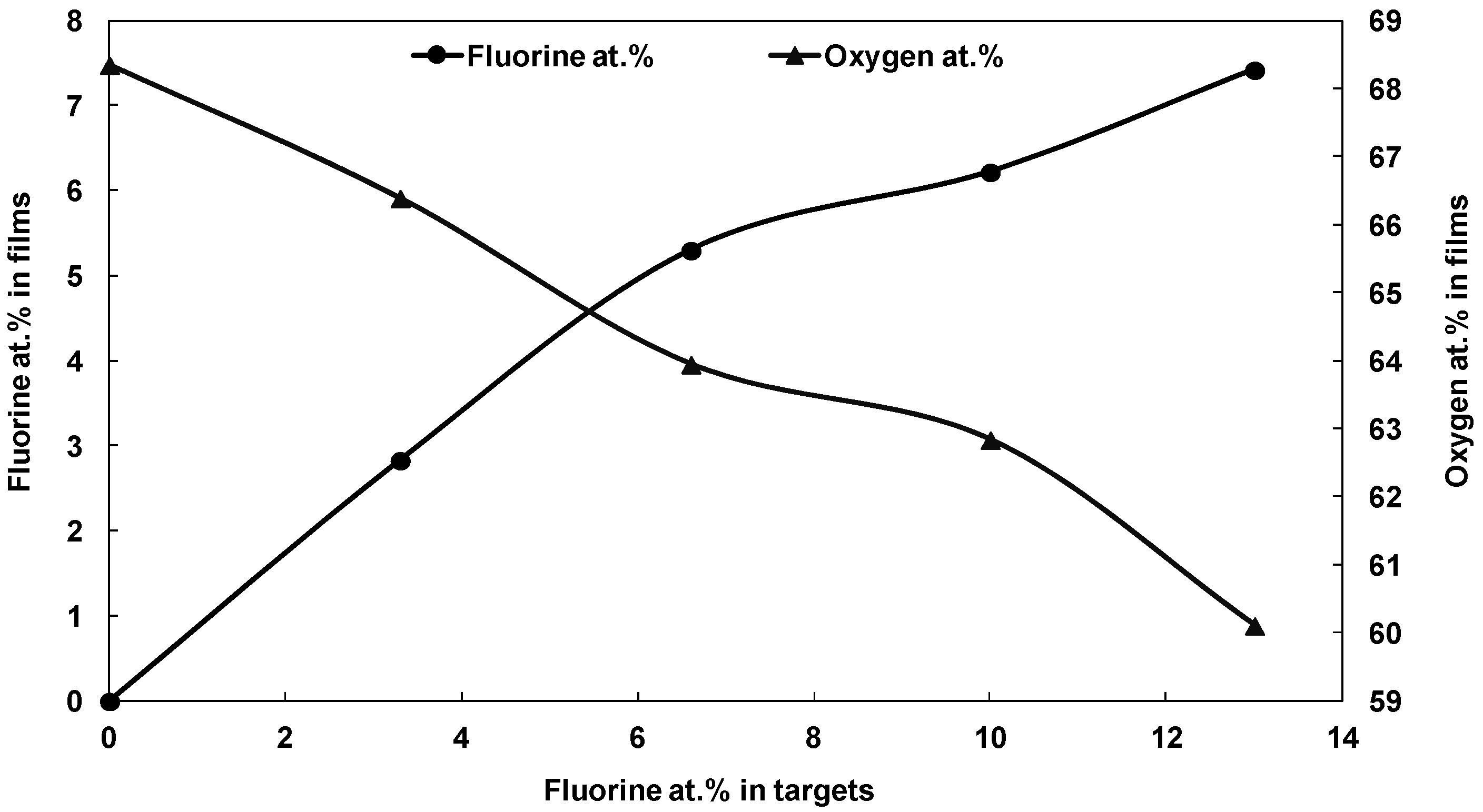
3.1. Elemental Analysis

The EDS absolute data from the analysis of the FTO films is given in Table 2. It is important to note that any oxygen detected from the glass substrate was not taken into consideration during the analysis of this study, because the energy of the EDS beam was optimized to be low enough not to detect the elements of glass such as Si and Ca and it was, therefore, also assumed not necessary to consider the oxygen arising from the glass substrate. The analysis of the un-doped tin oxide film shows a composition of 31.7 at.% tin and 68.4 at.% oxygen which is close to stoichiometric SnO2. It was observed that the fluorine content in the doped thin films is in the range of 0–7.4 at.%, which is low in comparison to the amount of fluorine incorporated into the powder targets (0–13 at.%). This can be explained by the fact that fluorine is a light element (Z = 9) and may be more readily scattered during gas phase transport through the high density plasma [19].
Table 2. compositional analysis of the powder targets and subsequent tin oxide and fluorine doped tin oxide.
Sample IDElement at.% in targetsElement at.% in filmsFilm thickness (nm)
OFSnOFSn
SnO266.70.033.468.40.031.7403
SnO2:F163.33.333.366.42.830.8410
SnO2:F260.06.633.364.05.330.7405
SnO2:F356.710.033.262.86.230.9415
SnO2:F453.413.033.360.17.432.5395
Figure 1 depicts the relationship between the fluorine and oxygen atomic content incorporated in the film, both as a function of the fluorine content of the target. It was observed that the fluorine to oxygen ratio increased with the increase in the fluorine content in the thin film. This indicates that the fluorine was successfully incorporated into the tin oxide, as each F anion substitutes an O2− anion in the lattice. This is attributed to the fact that fluorine is the most favored oxygen substitute, because the ionic size of fluorine (F:0.133 nm) is closely matched to that of oxygen (O2−:0.132 nm) [24].
Figure 1. Energy-dispersive X-ray spectroscopy (EDS) analysis of fluorine and oxygen atomic content in the fluorine doped tin oxide (FTO) films as a function of fluorine atomic content in the target.
Coatings 04 00732 g001

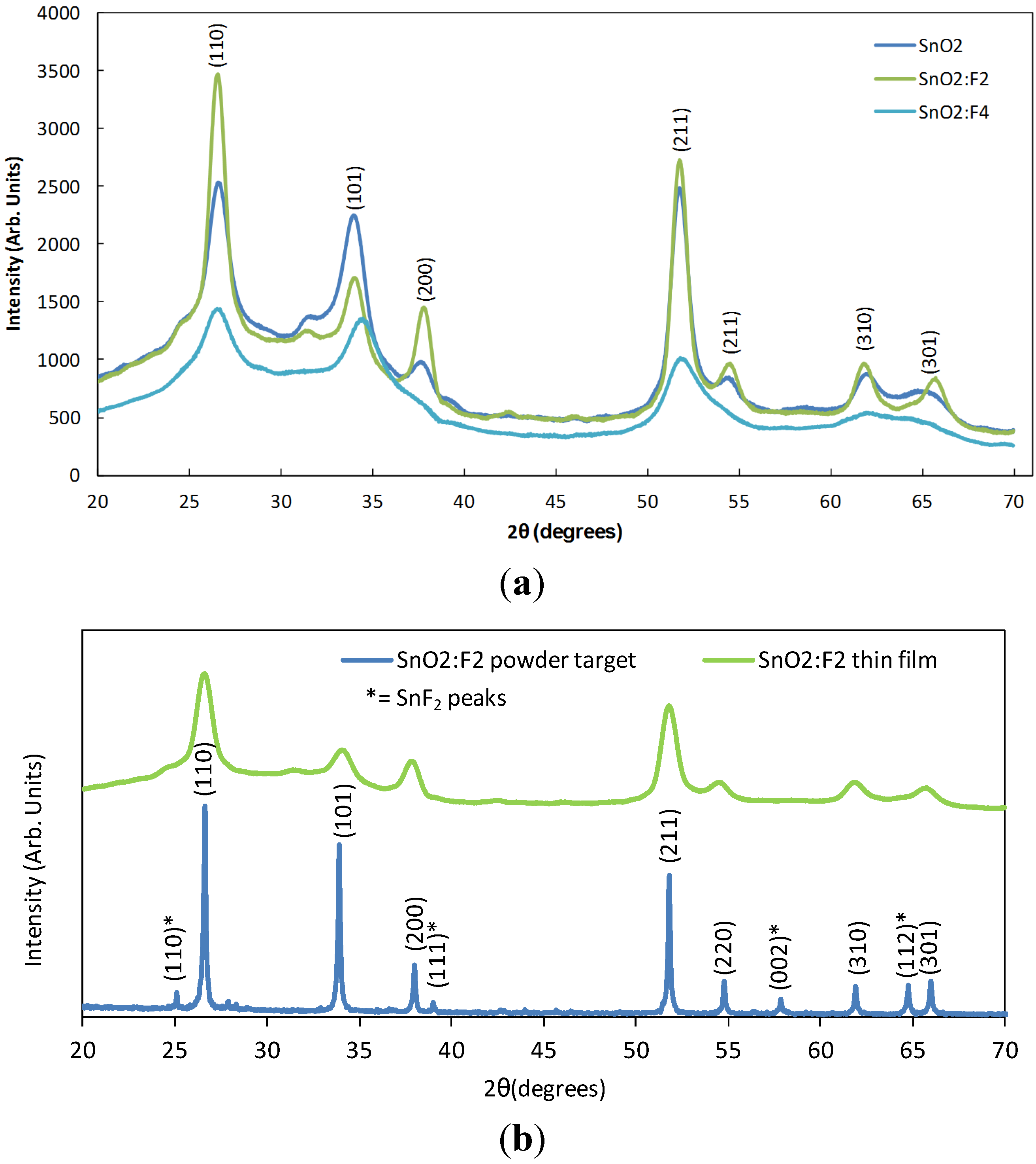
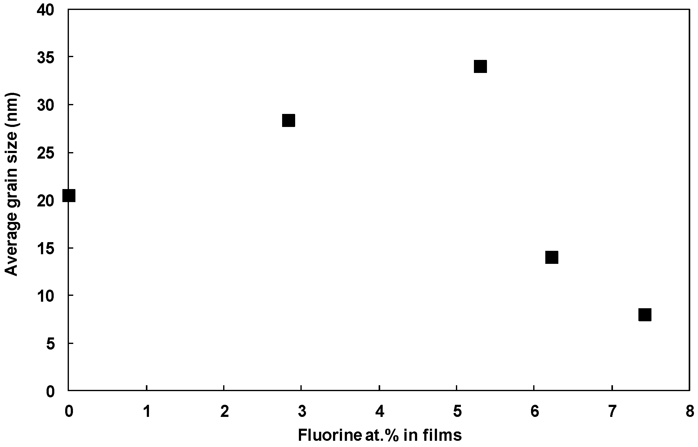
3.2. Structural Properties

The crystal structures of the SnO2 and SnO2:F thin films were analysed using X-ray diffraction over the range 20° to 70° 2θ. The XRD patterns for the SnO2, SnO2:F2 and SnO2:F4 (chosen as a representative example of the doped films) films are presented in Figure 2a. Also, Figure 2b shows a comparison between the spectra of the bulk powder target SnO2:F2 and the spectra of the as deposited SnO2:F2 thin film. The diffraction angle (2θ), Miller indices, grain size and texture coefficient for all the thin films are presented in Table 3.
Figure 2. X-ray diffraction patterns showing the (a) effect of doping on the crystallography of SnO2, SnO2:F2 and SnO2:F4 thin film samples on glass substrates, and (b) the comparison between the spectra of the SnO2:F2 bulk powder target and the SnO2:F2 thin film sample.
Coatings 04 00732 g002
Table 3. diffraction angle (2θ), the miller indices (hkl), grain size (D) and the texture coefficient (P) of FTO thin films.
Sample ID2θ (°)PeakLattice parametersGrain size DTexture coefficient P
(hkl)a (Å)c (Å)(nm)
SnO226.61104.743.35150.48
37.72004.752.37240.42
51.72114.321.77221.27
SnO2:F126.51104.793.39280.73
37.82004.772.38230.95
51.62114.341.77341.48
SnO2:F226.51104.793.38310.77
37.82004.812.4381.11
51.72114.321.77331.31
SnO2:F326.61104.773.38130.47
37.72004.782.39140.6
51.62114.341.77151.01
SnO2:F426.61104.813.490.3
51.42114.351.7870.49
From Figure 2a, it can be observed that the films exhibited XRD patterns with diffraction peaks corresponding to the (110), (101), (200), (211), (301), and (310) peaks of the rutile SnO2 pattern [25]. The presence of these peaks indicates that all the films were found to be of the cassiterite type with a polycrystalline structure. No other diffraction lines that correspond to other tin oxide or tin fluoride structures were detected in the thin film spectra, which indicates the O atoms were replaced by F atoms in the SnO2:F thin films [26]. It was evident from the comparison between the powder target spectra and that of the thin film sample, that the peaks marked corresponding to the SnF2 spectra marked with an asterisk were not present in the deposited thin film, which suggests that the fluorine atoms are fully incorporated into the tin oxide lattice. In addition, there was no significant shift in the peak positions of all the developed thin films, which probably implies that fluorine doping, did not introduce any significant stress in the films. It is apparent from Figure 2a that the un-doped SnO2 sample has a lower intensity in comparison to the sharper more intense peaks of SnO2:F2 sample. In another words, the crystallinity of the SnO2 samples were improved with the fluorine incorporation (2.8 to 5.3 at.%). In the present investigation, the intensity of the (200) plane ameliorates with the increase in the fluorine concentration up to 5.3 at.% and then deteriorated with fluorine concentration up to 7.4 at.% (sample SnO2:F4), a similar behaviour was observed by Moholkar et al. [27]. It is therefore concluded that the fluorine content strongly effects the structure of the SnO2, as observed elsewhere [28].
Thin films deposited via magnetron sputtering, usually exhibit a preferred orientation because the sputtered atoms arrive at the substrate via limited pathways, therefore promoting the formation of a columnar microstructure. A preferred orientation can also be affected by experimental parameters, such as the growth temperature [29,30], coating thickness [31] and fluorine doping level [9,11].
The intensity of the hkl reflection pattern can be utilised to determine the orientation of the grains or the volume of crystallites within that particular hkl plane parallel to the surface sample.
The degree of the preferred orientation of the thin films can be estimated by comparing the relative intensities of the measured peaks. A texture coefficient TC (hkl) is calculated using the Harris analysis technique shown in Equation (1) [32],
TC ( h k l ) = I ( h k l ) I o ( h k l ) × [ 1 n i = 1 n I ( h k l ) I o ( h k l ) ] 1
where I is the measured intensity of the peak, Io is the theoretical intensity obtained from the JCPDS powder diffraction file and n is the number of peaks. The texture coefficients for the (110), (200) and (211) peaks are shown in Table 3.
It is apparent from Table 3 that the coatings tend to have a (211) preferred orientation or texture (TC > 1). FTO coatings grown by other techniques suggest that the (200) peak was most influenced by fluorine doping [18]. Although the TC of the (200) peak varies with fluorine content, becoming a maximum of 1.11 at 5.3 at.% F, it still remains below the TC for the (211) peak.
The grain sizes of the crystallites were calculated using the Scherrer equation shown in Equation (2) for the (110), (211) and (200) peaks [33]. It is important to note that a lattice strain de-convolution was not considered during the calculation.
D = 0.9 λ β cos θ
where D is the grain size, λ is the wavelength of the X-ray source used, β is the full width half maximum (FWHM) of the specific peak, θ is the Bragg angle of that peak. The calculated values are presented in Table 3.
The average of the grain sizes for the (110), (200) and (211) peaks is shown in Figure 3. It was observed that the mean crystallite size followed a progressive incremental trend with increasing fluorine content up to 5.3 at.% (from 20 nm to 34 nm). Similar trends were observed by Mientus et al. which showed an increase in the grain size from 12 to 25 nm [10], also similar trend was observed by Kim et al. which showed an increase in the grain size from 4 to 30 nm [9]. Beyond 5.3 at.% of fluorine in the thin film, there was a reduction in the crystallite size, which may be due to the excess fluorine within the tin oxide lattice. The implication being that 5.3 at.% of fluorine in the lattice was the optimum composition, of those tested, for grain growth.
The calculated values for the lattice parameters “a” and “c” for SnO2 thin films are 4.74 Å and 3.35 Å for the (110) peak which are in reasonable agreement with the standard data (a = 4.73 Å, c = 3.18 Å) [25].
Figure 3. Average grain size variation as a function of fluorine atomic content in the FTO thin films.
Coatings 04 00732 g003

3.3. Electrical Properties

To characterise the electrical properties of the thin films, Hall Effect probe measurements in a Van der Pauw configuration at room temperature were employed [34]. Figure 4 presents the electrical behaviour of the thin films as a function of the fluorine content. The values for the carrier concentration (Nd) were reported to be negative, however, the absolute value was plotted to present the trend of the data.
Resistivity and mobility values of 3.71 × 10⁻¹ Ω·cm and 3.1 cm2/Vs and a corresponding carrier concentration (Nd) of 5.5 × 1018 cm−3 were obtained for un-doped SnO2. These values are similar to those reported elsewhere [10,12]. It was observed from the carrier concentration (Nd) data that the FTO thin films exhibit n-type conductivity which is also achieved by other deposition techniques including spray pyrolysis and PLD [2,9].
It was observed from Figure 4, that the best electrical properties where achieved with a fluorine concentration of 5.3 at.%, corresponding to a resistivity of 6.71 × 10⁻³ Ω·cm, mobility of 15.1 cm2/Vs and a carrier concentration (Nd) of 1.46 × 1020 cm−3 for the films. Similar results were achieved by PLD at a deposition temperature of 300 °C [9]. The improvement in the electrical properties is attributed to the larger grain size observed at this composition [9]. In addition, the hybrid orbital configuration of fluorine and oxygen are 2S22P5 and 2S22P4, respectively, indicating that fluorine atoms promote one free electron/ molecule when it sits in place of oxygen. As the ionic radius of F (1.36 Å) is slightly lower than that of O2− (1.40 Å), so the fluorine atoms are more electronegative than the oxygen atoms, therefore the fluorine substitutes the oxygen sites more easily [35]. This phenomenon leads to higher carrier concentration, which is shown in Figure 4. Similar trends were observed in [4].
Figure 4. Variation of: (a) resistivity in logarithmic scale; (b) mobility; and (c) absolute carrier concentration of FTO thin films as a function of fluorine atomic content.
Coatings 04 00732 g004
Increasing the fluorine content in the film beyond 5.3 at.% resulted in a degradation of the electrical properties. This is probably attributed to the solubility limit of fluorine into the tin oxide lattice [11], and probably the cause for the reduction in the grain size, as observed in Table 3 [3]. The excess fluorine atoms do not occupy the correct position within the lattice, which leads to disorder of the structure, grain boundary scattering and therefore to a decrease in the free carrier concentration (Nd) and mobility and an increase in the resistivity (7.04 × 1019 cm−3, 10.15 cm2/Vs and 1.31 × 10⁻¹ Ω·cm, respectively). The effect of the fluorine content on the electrical properties of FTO was investigated by Elangovan et al., who reported the degradation in the electrical properties is probably due to the solubility limit of fluorine content in the thin film [11]. Kim et al. found that a saturation carrier concentration (Nd) is achieved due to the formation of Sn-F complexes in the grain boundaries when using higher than 10 wt.% of SnF2 in target [9]. The electrical results depicted in this study indicate that the mobility and the carrier concentration (Nd) were limited by the solubility limit of fluorine content in the film. This behaviour is also observed by Elangovan et al. [11].

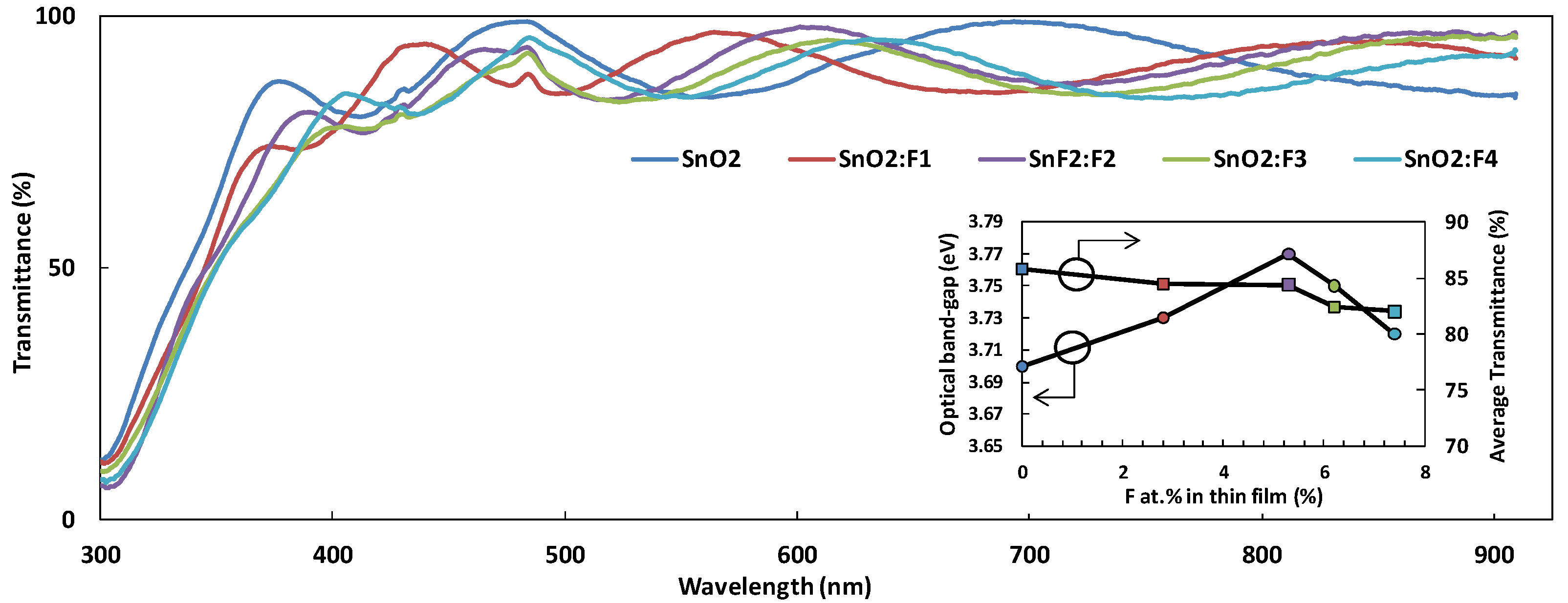
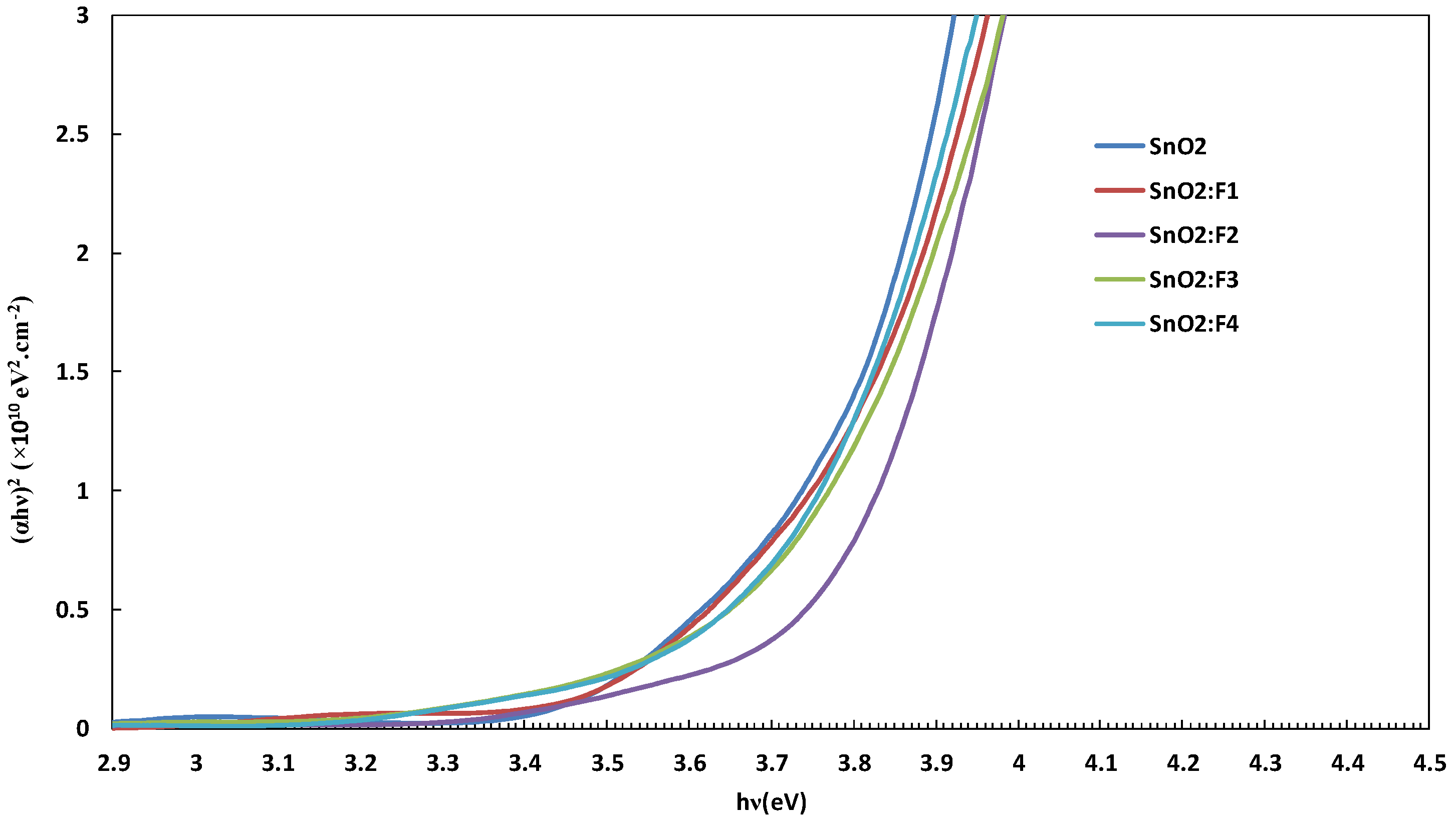
3.4. Optical Properties

The optical transmittance and the direct band-gap properties of SnO2:F films as a function of fluorine content in the thin films are presented in Figure 5 and Figure 6, respectively. The transmittance data of each sample was recorded three times and an average taken. The optical transmittance (T) was averaged over the wavelength range of 300–900 nm, and the absorption coefficient (α) was determined by using Equation (3),
T e α t
where, t is the thickness of the film. The absorption refers to the excitation of an electron from the valence band to the conduction band. The absorption coefficient was then used to estimate the direct optical energy band-gap (Eg) using the relation shown in Equation (4),
α h ν = C ( h ν E g ) 1 / 2
where h is Planck’s constant, ν is the frequency of the incident photon, C is a constant for direct transition and α is the absorption coefficient. The direct optical energy band-gap (Eg) was estimated by extrapolating the linear portion of the curve (αhν)2 against (hν) for direct allowed transition to the point where αhν = 0 [36].
The optical transmission spectra recorded in the wavelength range of 300 to 900 nm are presented in Figure 5. High transparency in the visible range (82 < Tvis < 85) was observed, in accordance with the requirements for TCO applications (80%) [37]. This can be associated with good structural homogeneity. It is evident from the Figure 5; the average visible transmittance is not influenced much for different doping levels of fluorine, similar behaviour was also observed in [35] and [38]. However, a slight decrease in the transmission is probably due to the decrease in the oxygen vacancies as perceived in the EDS data shown in Table 2. The insert in Figure 5 is for the convenience of the reader to give a quick average view of the transmission and the direct optical band-gap against the change in the fluorine concentration in the thin film. The sharp decrease in the transmission in the UV range of the spectrum is related to the light absorption edge [39]. It is also possible to notice that both the un-doped and the doped films showed interference fringes pattern, suggesting that there is little scattering losses at the surface.
Figure 5. The optical transmittance of FTO thin films as a function of fluorine atomic content. The insert shows the variation in optical band-gap and the average transmittance across the 300 ≤ λ ≤ 900 nm with change in fluorine concentration in thin film.
Coatings 04 00732 g005
The direct band-gap for un-doped tin oxide was estimated to be 3.70 eV, which increased slightly to a value of 3.77 eV at a fluorine content of 5.4 at.% in the film as observed in Figure 6. The direct band-gap values obtained in this work are slightly higher than the direct band-gap values of 3.17–3.45 eV reported in [11] and slightly lower than the band-gap values of 4.0–4.25 eV reported in [9]. This variation is probably attributed to the different concentration of fluorine used in the film, the thickness variation and the experimental variables such as working pressure and deposition temperature.
Figure 6. The direct allowed transition of FTO thin films as a function of fluorine atomic content.
Coatings 04 00732 g006
Generally, the band-gap energy for doped metal oxides films is higher than that of the un-doped type. This is because the energy gap between the valence band and the lowest empty state in the conduction band is found to increase due to the filling of low lying energy levels in the conduction that is caused by the increase in the carrier concentration (Burstein-Moss effect) [37]. The shift in the band-gap can also be related to the variation in the mean crystallite size, the internal stress or due to the free carrier concentration [40].

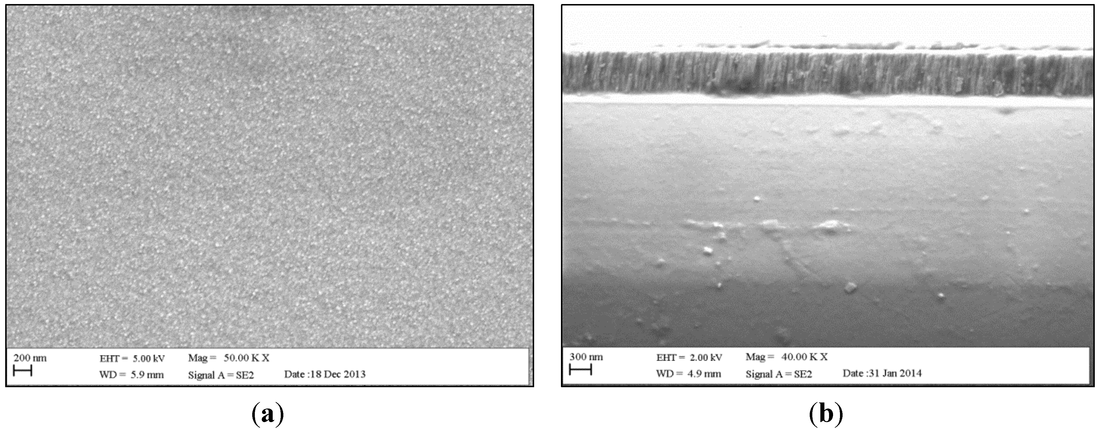
3.5. Morphological Properties

Figure 7a,b shows the surface area and the cross-section SEM morphologies of SnO2:F2 film, respectively. The film has a compact and dense homogenous surface characterised by small grains. The small grains observed in Figure 7a are probably a result of the low deposition temperature. Consonni et al. studied the effect of deposition temperature and observed an increase in the mean grain size from 60 to 127 nm as the growth temperature raised from 360 to 460 °C.
The thickness of the film was measured to be about 410 nm, which is in a good agreement with the Dektak profilometer measurements. The cross-sectional images show that the thin film has a dense columnar grained structure normal to the surface of the substrate.
Figure 7. (a) Surface and (b) cross-sectional SEM morphologies of SnO2:F2 thin film.
Coatings 04 00732 g007

4. Conclusions

Transparent conductive oxide SnO2:F thin films have been deposited on glass substrates by the pulsed DC magnetron sputtering technique in an Ar/O2 atmosphere using loosely packed blended powder targets. The thin films were grown at a deposition rate of 27 nm·min−1 and a deposition temperature below 170 °C. It was determined that 5.3 at.% of fluorine incorporated into the film gave the best electrical behavior. In addition, the XRD structural analysis showed that the crystallinity of the SnO2 samples were improved with the fluorine incorporation and the intensity of the (200) plane ameliorated with the increase in the fluorine concentration up to 5.3 at.% found in the thin film. The average optical transmittance achieved for this coating was 83% across a range of 300 ≤ λ ≤ 900 nm. The detailed analysis of the electrical properties of the thin film as a function of the fluorine doping level revealed that a resistivity as low as 6.71 × 10⁻³ Ω·cm was obtained with a fluorine content of 5.3 at.%.
This work has shown the ability to grow transparent conductive oxide SnO2:F thin films using a cost effective (no post annealing of samples, and high deposition rate) and environmentally friendly method (no fluorine gas is used and no toxic affluent is produced). This technique is of great advantage for studying the properties of multicomponent materials and identifying optimum compositions.

Acknowledgments

This work was supported by the Engineering and Physical Science Research Council (EPSRC). The authors would like to thank Hayley Andrews for providing assistance on the FE-SEM and the EDAX software.

Author Contributions

Ziad Y. Banyamin conducted the experiments and was the lead author. Peter J. Kelly and Glen West were the supervisory team for the experimental programmes described here. Jeffery Boardman acted as the external consultant.

Conflicts of Interest

The authors declare no conflict of interest.

References

  1. Cachet, H. Films and powders of fluorine-doped tin dioxide. In Fluorinated Materials for Energy Conversion; Tsuyoshi, N., Henri, G., Eds.; Elsevier Science: Amsterdam, The Netherlands, 2005; pp. 513–534. [Google Scholar]
  2. Subba Ramaiah, K.; Sundara Raja, V. Structural and electrical properties of fluorine doped tin oxide films prepared by spray-pyrolysis technique. Appl. Surf. Sci. 2006, 253, 1451–1458. [Google Scholar]
  3. Tesfamichael, T.; Will, G.; Colella, M.; Bell, J. Optical and electrical properties of nitrogen ion implanted fluorine doped tin oxide films. Nucl. Instrum. Methods Phys. Res. B Beam Interact. Mater. Atoms 2003, 201, 581–588. [Google Scholar] [CrossRef] [Green Version]
  4. Kim, C.-Y.; Riu, D.-H. Texture control of fluorine-doped tin oxide thin film. Thin Solid Films 2011, 519, 3081–3085. [Google Scholar] [CrossRef]
  5. Gerhardinger, P.F.; McCurdy, R.J. Float line deposited transparent conductors—Implications for the PV industry. MRS Proc. 1996, 426, 399–410. [Google Scholar] [CrossRef]
  6. Sankara Subramanian, N.; Santhi, B.; Sundareswaran, S.; Venkatakrishnan, K.S. Studies on spray deposited SnO2, Pd:SnO2 and F:SnO2 thin films for gas sensor applications. Synth. React. Inorg. Metal-Org. Nano-Metal Chem. 2006, 36, 131–135. [Google Scholar]
  7. Yadav, A.A.; Masumdar, E.U.; Moholkar, A.V.; Neumann-Spallart, M.; Rajpure, K.Y.; Bhosale, C.H. Electrical, structural and optical properties of SnO2:F thin films: Effect of the substrate temperature. J. Alloy. Compd. 2009, 488, 350–355. [Google Scholar] [CrossRef]
  8. Sheel, D.W.; Gaskell, J.M. Deposition of fluorine doped indium oxide by atmospheric pressure chemical vapour deposition. Thin Solid Films 2011, 520, 1242–1245. [Google Scholar] [CrossRef]
  9. Kim, H.; Auyeung, R.C.Y.; Piqué, A. Transparent conducting F-doped SnO2 thin films grown by pulsed laser deposition. Thin Solid Films 2008, 516, 5052–5056. [Google Scholar] [CrossRef]
  10. Mientus, R.; Ellmer, K. Structural, electrical and optical properties of SnO2−x:F-layers deposited by DC-reactive magnetron-sputtering from a metallic target in Ar–O2/CF4 mixtures. Surf. Coat. Technol. 1998, 98, 1267–1271. [Google Scholar] [CrossRef]
  11. Elangovan, E.; Ramamurthi, K. Studies on micro-structural and electrical properties of spray-deposited fluorine-doped tin oxide thin films from low-cost precursor. Thin Solid Films 2005, 476, 231–236. [Google Scholar] [CrossRef]
  12. Gorley, P.M.; Khomyak, V.V.; Bilichuk, S.V.; Orletsky, I.G.; Horley, P.P.; Grechko, V.O. SnO2 films: Formation, electrical and optical properties. Mater. Sci. Eng. B 2005, 118, 160–163. [Google Scholar] [CrossRef]
  13. Maruyama, T.; Akagi, H. Fluorine-doped tin dioxide thin films prepared by radio-frequency magnetron sputtering. J. Electrochem. Soc. 1996, 143, 283–287. [Google Scholar] [CrossRef]
  14. Martel, A.; Caballero-Briones, F.; Fandiño, J.; Castro-Rodrı́guez, R.; Bartolo-Pérez, P.; Zapata-Navarro, A.; Zapata-Torres, M.; Peña, J.L. Discharge diagnosis and controlled deposition of SnOx:F films by DC-reactive sputtering from a metallic tin target. Surf. Coat. Technol. 1999, 122, 136–142. [Google Scholar] [CrossRef]
  15. Zhou, Y. The Production and Properties of TCO Coatings Prepared by Pulsed Magnetron Sputtering from Powder Targets. Ph.D. Thesis, University of Salford, Manchester, UK, 2004. [Google Scholar]
  16. Kelly, P.J.; Zhou, Y. Zinc oxide-based transparent conductive oxide films prepared by pulsed magnetron sputtering from powder targets: Process featuresand film properties. J. Vac. Sci. Technol. A 2006, 24, 1782–1785. [Google Scholar] [CrossRef]
  17. Zhou, Y.; Kelly, P.J.; Postill, A.; Abu-Zeid, O.; Alnajjar, A.A. The characteristics of aluminium-doped zinc oxide films prepared by pulsed magnetron sputtering from powder targets. Thin Solid Films 2004, 447–448, 33–39. [Google Scholar] [CrossRef]
  18. Exarhos, G.J.; Zhou, X.-D. Discovery-based design of transparent conducting oxide films. Thin Solid Films 2007, 515, 7025–7052. [Google Scholar] [CrossRef]
  19. Čada, M.; Bradley, J.W.; Clarke, G.C.B.; Kelly, P.J. Measurement of energy transfer at an isolated substrate in a pulsed dc magnetron discharge. J. Appl. Phys. 2007, 102. [Google Scholar] [CrossRef]
  20. Alkoy, E.M.; Kelly, P.J. The structure and properties of copper oxide and copper aluminium oxide coatings prepared by pulsed magnetron sputtering of powder targets. Vacuum 2005, 79, 221–230. [Google Scholar] [CrossRef]
  21. Kelly, P.J.; Zhou, Y.; Postill, A. A novel technique for the deposition of aluminium-doped zinc oxide films. Thin Solid Films 2003, 426, 111–116. [Google Scholar] [CrossRef]
  22. Audronis, M.; Kelly, P.J.; Arnell, R.D.; Leyland, A.; Matthews, A. The structure and properties of chromium diboride coatings deposited by pulsed magnetron sputtering of powder targets. Surf. Coat. Technol. 2005, 200, 1366–1371. [Google Scholar] [CrossRef]
  23. Hartnagel, H.L.; Dawar, A.L.; Jain, A.K.; Jagadish, C. Semiconducting Transparent Thin Films; Institute of Physics: Bristol, UK, 1995; pp. 223–234. [Google Scholar]
  24. Elangovan, E.; Singh, M.P.; Ramamurthi, K. Studies on structural and electrical properties of spray deposited SnO2:F thin films as a function of film thickness. Mater. Sci. Eng. B 2004, 113, 143–148. [Google Scholar] [CrossRef]
  25. Joint Committee on Powder Diffraction Standards (JCPDS); International Centre for Diffraction Data: Newtown Square, PA, USA, 1997.
  26. Ren, Y.; Zhao, G.; Chen, Y. Fabrication of textured SnO2:F thin films by spray pyrolysis. Appl. Surf. Sci. 2011, 258, 914–918. [Google Scholar] [CrossRef]
  27. Moholkar, A.V.; Pawar, S.M.; Rajpure, K.Y.; Bhosale, C.H.; Kim, J.H. Effect of fluorine doping on highly transparent conductive spray deposited nanocrystalline tin oxide thin films. Appl. Surf. Sci. 2009, 255, 9358–9364. [Google Scholar] [CrossRef]
  28. Bilgin, V.; Akyuz, I.; Ketenci, E.; Kose, S.; Atay, F. Electrical, structural and surface properties of fluorine doped tin oxide films. Appl. Surf. Sci. 2010, 256, 6586–6591. [Google Scholar] [CrossRef]
  29. Consonni, V.; Rey, G.; Roussel, H.; Doisneau, B.; Blanquet, E.; Bellet, D. Preferential orientation of fluorine-doped SnO2 thin films: The effects of growth temperature. Acta Mater. 2013, 61, 22–31. [Google Scholar] [CrossRef]
  30. Fukano, T.; Motohiro, T. Low-temperature growth of highly crystallized transparent conductive fluorine-doped tin oxide films by intermittent spray pyrolysis deposition. Sol. Energy Mater. Sol. Cells 2004, 82, 567–575. [Google Scholar]
  31. Agashe, C.; Hüpkes, J.; Schöpe, G.; Berginski, M. Physical properties of highly oriented spray-deposited fluorine-doped tin dioxide films as transparent conductor. Sol. Energy Mater. Sol. Cells 2009, 93, 1256–1262. [Google Scholar] [CrossRef]
  32. Barratt, C.S.; Massalski, T.B. Structure of Metals; Pergamon Press: Oxford, UK, 1980. [Google Scholar]
  33. Mamazza, R., Jr.; Morel, D.L.; Ferekides, C.S. Transparent conducting oxide thin films of Cd2SnO4 prepared by RF magnetron co-sputtering of the constituent binary oxides. Thin Solid Films 2005, 484, 26–33. [Google Scholar] [CrossRef]
  34. Van der Pauw, L.J. A method of measuring specific resistivity and hall effec of discs of arbitrary shape. Philips. Res. Repts. 1958, 13, 334. [Google Scholar]
  35. Bhuvaneswari, P.V.; Velusamy, P.; Babu, R.R.; Babu, S.M.; Ramamurthi, K.; Arivanandhan, M. Effect of fluorine doping on the structural, optical and electrical properties of spray deposited cadmium stannate thin films. Mater. Sci. Semicond. Proc. 2013, 16, 1964–1970. [Google Scholar] [CrossRef]
  36. Tauc, J.; Grigorovici, R.; Vancu, A. Optical properties and electronic structure of amorphous germanium. Phys. Status Solidi (b) 1966, 15, 627–637. [Google Scholar] [CrossRef]
  37. Guillén, C.; Herrero, J. TCO/metal/TCO structures for energy and flexible electronics. Thin Solid Films 2011, 520, 1–17. [Google Scholar]
  38. Arefi-Khonsari, F.; Bauduin, N.; Donsanti, F.; Amouroux, J. Deposition of transparent conductive tin oxide thin films doped with fluorine by PACVD. Thin Solid Films 2003, 427, 208–214. [Google Scholar] [CrossRef]
  39. Shanthi, S.; Anuratha, H.; Subramanian, C.; Ramasamy, P. Effect of fluorine doping on structural, electrical and optical properties of sprayed SnO2 thin films. J. Crys. Growth 1998, 194, 369–373. [Google Scholar] [CrossRef]
  40. Elangovan, E.; Ramamurthi, K. A study on low cost-high conducting fluorine and antimony-doped tin oxide thin films. Appl. Surf. Sci. 2005, 249, 183–196. [Google Scholar] [CrossRef]

