Article

Translation Effects in Fluorine Doped Tin Oxide Thin Film Properties by Atmospheric Pressure Chemical Vapour Deposition

Materials and Physics Research Centre, The University of Salford, M5 4WT Salford, UK
*
Author to whom correspondence should be addressed.
Coatings 2016, 6(4), 43; https://doi.org/10.3390/coatings6040043
Submission received: 13 September 2016 / Revised: 29 September 2016 / Accepted: 8 October 2016 / Published: 12 October 2016
(This article belongs to the Special Issue Chemical Vapor Deposition)

Abstract

:
In this work, the impact of translation rates in fluorine doped tin oxide (FTO) thin films using atmospheric pressure chemical vapour deposition (APCVD) were studied. We demonstrated that by adjusting the translation speeds of the susceptor, the growth rates of the FTO films varied and hence many of the film properties were modified. X-ray powder diffraction showed an increased preferred orientation along the (200) plane at higher translation rates, although with no actual change in the particle sizes. A reduction in dopant level resulted in decreased particle sizes and a much greater degree of (200) preferred orientation. For low dopant concentration levels, atomic force microscope (AFM) studies showed a reduction in roughness (and lower optical haze) with increased translation rate and decreased growth rates. Electrical measurements concluded that the resistivity, carrier concentration, and mobility of films were dependent on the level of fluorine dopant, the translation rate and hence the growth rates of the deposited films.

1. Introduction

Investigations into the deposition of transparent conducting oxide (TCO) thin films as electrodes are mainly driven by their high optical transparency in the visible region and high electrical conductivity [1], essential for enhanced power conversion efficiencies. These properties have made TCOs the material of choice for many high-tech applications including solar cells, [2] low emissivity windows, [3] light emitting diodes, [4] and smart windows [5].
Scarcity and high price of indium needed for indium tin oxide, the most popular TCO, has led to a worldwide effort to find low-cost alternatives with similar or improved properties. In particular, fluorine-doped tin dioxide (FTO) is not only an inexpensive substitute, but also demonstrates the desired optical and electrical characteristics and can be deposited by atmospheric pressure chemical vapour deposition (APCVD) [6,7,8]. The APCVD technique is highly favoured in industry e.g., in float glass production, due to high volume, low operating costs, improved film quality (hardness and adhesion), and fast deposition rates. Being a continuous, in-line, rather than batch process also eliminates the need to stop and start the deposition of materials. This yields films with a range of properties such as thicknesses and growth rates by careful adjustment of the experimental parameters.
The TCO properties are essential for modern solar cell structures and profoundly influence the energy conversion efficiencies. The surface morphologies coupled with low resistivity and high transparency play a key role in maximising both the amount of light reaching the absorber layer and hence the efficiency with which the excitons are generated [9]. In our previous work, we successfully deposited highly textured FTO layers by APCVD for silicon based solar cells, without any additional, post-deposition treatment such as etching [10,11]. However, the same FTO coatings are highly undesirable for dye-sensitised solar cells [12] and perovskite solar cells, primarily due to their relatively high surface roughness (e.g., from the naturally formed pyramidal shape in FTO deposited by APCVD), which is, however, an advantage for silicon based solar cells as it leads to enhanced light scattering and hence improved cell efficiency. In the case of perovskite based solar cells, the over-riding need is for smoother surfaces as too rough a surface could lead to non-uniform blocking layers and/or absorbing layers coverage and hence to shunt formation within the cells. As a result, it is of importance to optimise deposition conditions for fabricating thin FTO films with smoother morphologies. It is worth mentioning here that any improvement or adjustment in surface roughness most likely will be a result of compromise between film thickness (roughness), transparency, and conductivity [13]. The surface morphology is linked to other important characteristics of films, in particular the level of crystallographic orientation and the sheet resistance. Films with various electrical and optical properties have been reported for aluminium doped zinc oxide (ZnO) thin films by controlling the translation rate in the APCVD process [14]. According to the best of our knowledge, no studies have been conducted for the FTO thin film properties, probably due to lack of functionality within the process. Ma and co-workers used the in-line APCVD process for FTO thin films involving a conveyor furnace, tin tetrachloride, and difluoroethane but no translation effects were reported [15,16]. For the first time, we discuss here the critical properties needed to tailor FTO films to suit a range of solar cell applications. We produced and studied FTO films by altering the APCVD deposition parameters. These included the translation speeds of the susceptor under the coating head, dopant levels and different tin (Sn) precursor to water (H2O) molar ratios, 1:5 and 1:30. It was important to choose the appropriate translating distance to minimize heat losses and reactor blockages. The experiments were conducted on our APCVD coater which involved the use of monobutyltin trichloride (MBTC) as a Sn precursor. Many other Sn precursors are available, but MBTC was chosen because of its previously shown ability to yield films with low resistivity [11,17].

2. Experimental Section

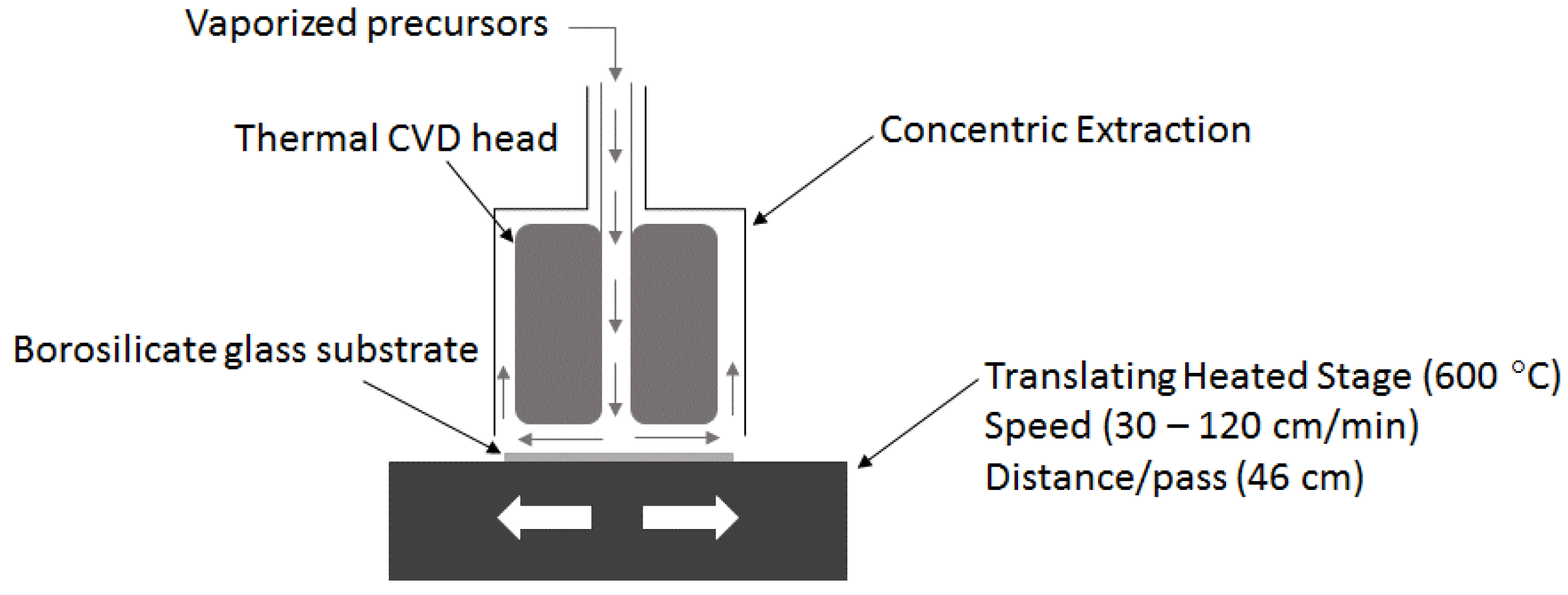
2.1. Deposition of Thin Films

All the chemicals were purchased from Sigma Aldrich Ltd. (Dorset, UK) and used as received. Prior to conducting deposition experiments, 1.1 mm borosilicate glass substrates (Corning Eagle 2000) were cleaned with detergent, water, propan-2-ol, and dried in air.
Thin films of SnO2:F was deposited by APCVD at a deposition temperature of 600 °C using MBTC with 0.2 or 0.6 M aqueous trifluoroacetic acid (TFAA), delivered with a Sn precursor to H2O molar ratio of 1:5 or 1:30. The APCVD system was purged under constant nitrogen (N2) for few hours, before carrying out any coatings. Precursors were vaporized using either bubbler (MBTC at 125 °C, 0.6 L·min−1 carrier gas) or flash evaporation (TFAA/water mix, 0.7 L·min−1 carrier gas). N2 was used as the carrier gas, with 15% oxygen at a total flow of 1.5 L·min−1. An APCVD gas handling system combined with a single flow coating head was employed which simulated a possible production-type process configuration. A heated susceptor was translated under the static CVD head in an extracted, open atmosphere, enclosure. This allowed the deposition of films over 10 × 10 cm2 (± 2%) area with good uniformity. To deposit films of similar thicknesses for each doping level, the number of passes (4, 8 or 16) under the CVD coating head was adjusted. A range of different translation speeds was used to change the precursor residence time over the substrate. A schematic illustration of the coating head is shown in Figure 1 and a summary of conditions is given in Table 1.

2.2. Characterization

X-ray diffraction (XRD) patterns were measured on a Bruker D8 using a Cu Kα source. The particle sizes were calculated using Scherrer Equation (1) [18] and texture coefficients were determined using Equation (2) [19]. Scanning electron microscope (SEM) images were recorded on a Quanta 250 ESEM. The surface roughness and morphologies were analysed by atomic force microscopy (NanoScope IIIa, Digital Inst. Ltd., Santa Barbara, CA, USA) over a 5 × 5 μm2 area. The film thickness was determined using a Dektak 3ST surface profiler (Veeco, Santa Barbara, CA, USA) by measuring at least five different points on the step etched film. Before such measurements, films were step etched using zinc powder and hydrochloric acid. Hall effect measurements were performed on the TCO films to determine the carrier concentration and the electron mobility with a lab built system using an electromagnetic with a pole separation of 10 mm and current of 1 A to give a magnetic flux density of 0.79 T. A lab built spectrometer consisting of a 75 W xenon lamp and four broadband filters centring on four wavelengths (800, 650, 531, and 450 nm) was used to measure optical properties. A silica sample was used to calibrate the throughput of the integrating sphere.
D = 0.94 λ β cos θ
where D is the size of the crystallites, β is the broadening of diffraction line measured at half its maximum intensity and λ is the wavelength of X-rays (1.54056 Å).
TC ( h k l ) = I ( h k l ) / I 0 ( h k l ) 1 n I ( h k l ) / I 0 ( h k l )
where I (hkl) and I0 (hkl) are the measured intensity and standard integrated intensity (from JCPDS No. 021-1250) for (hkl) reflection, respectively, and n is the number of reflections observed.

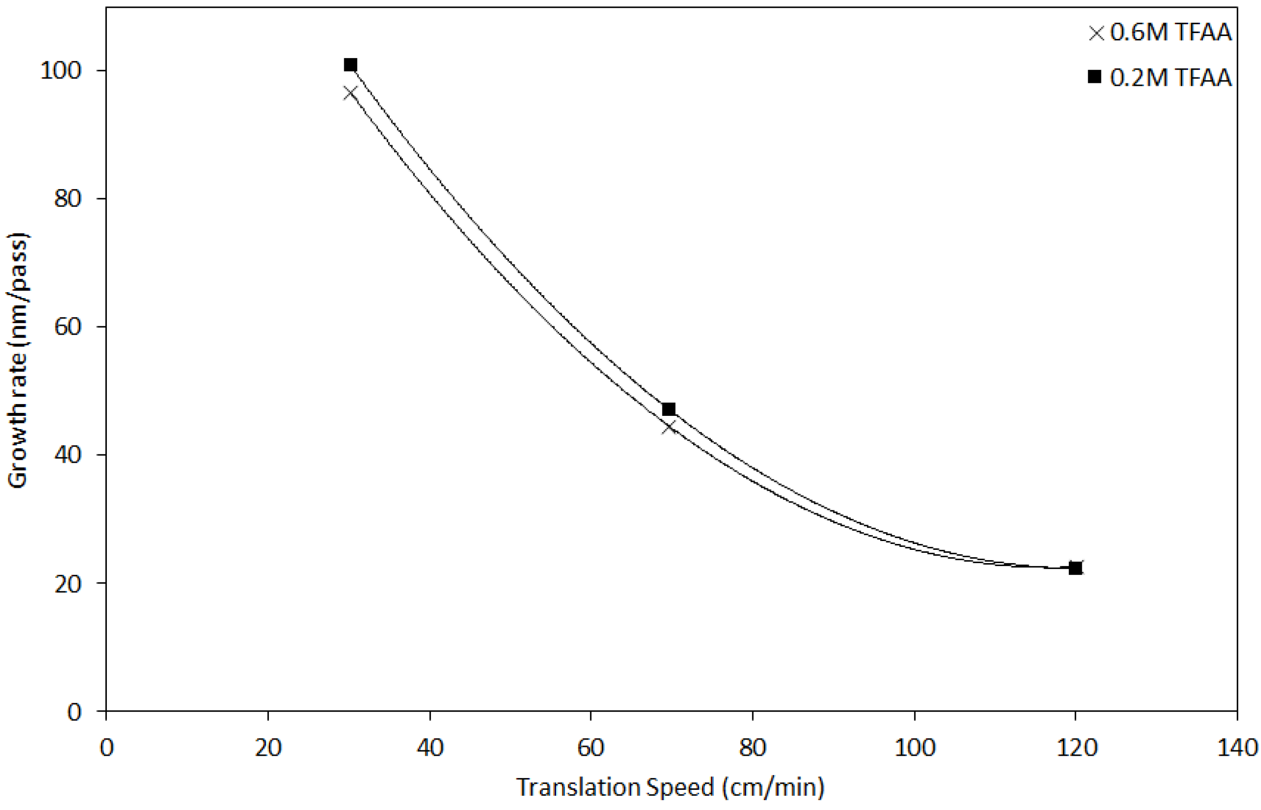
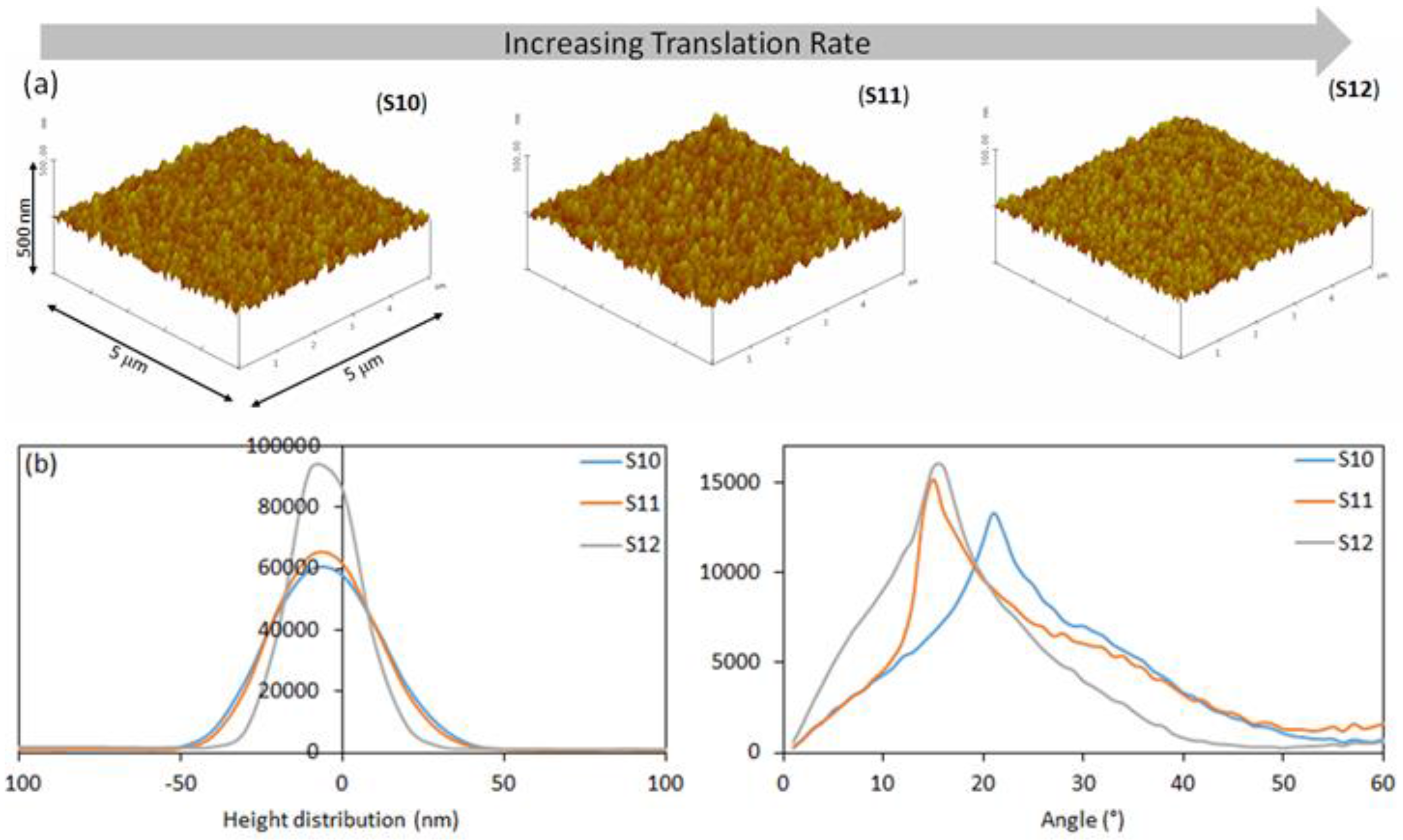
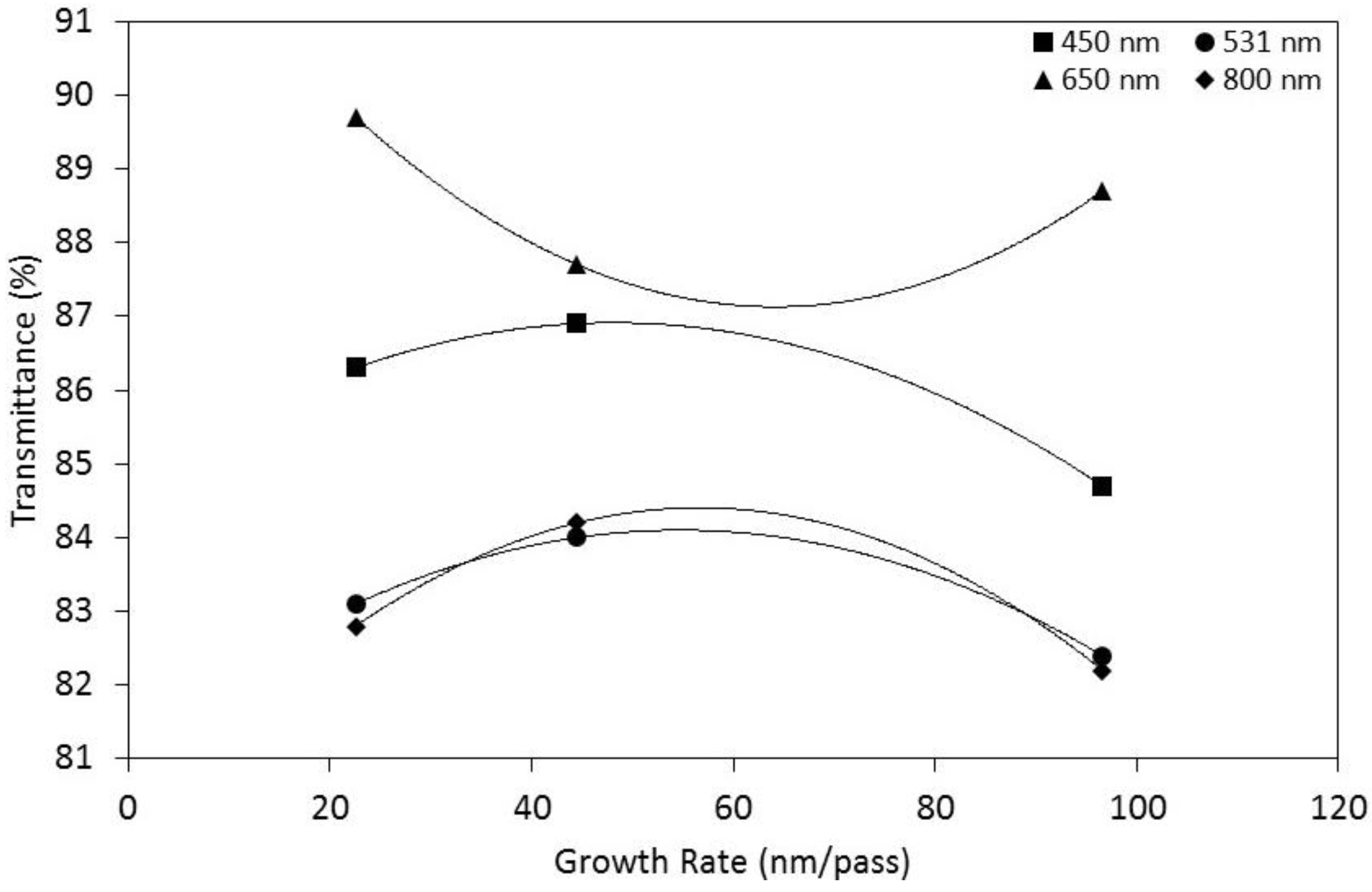
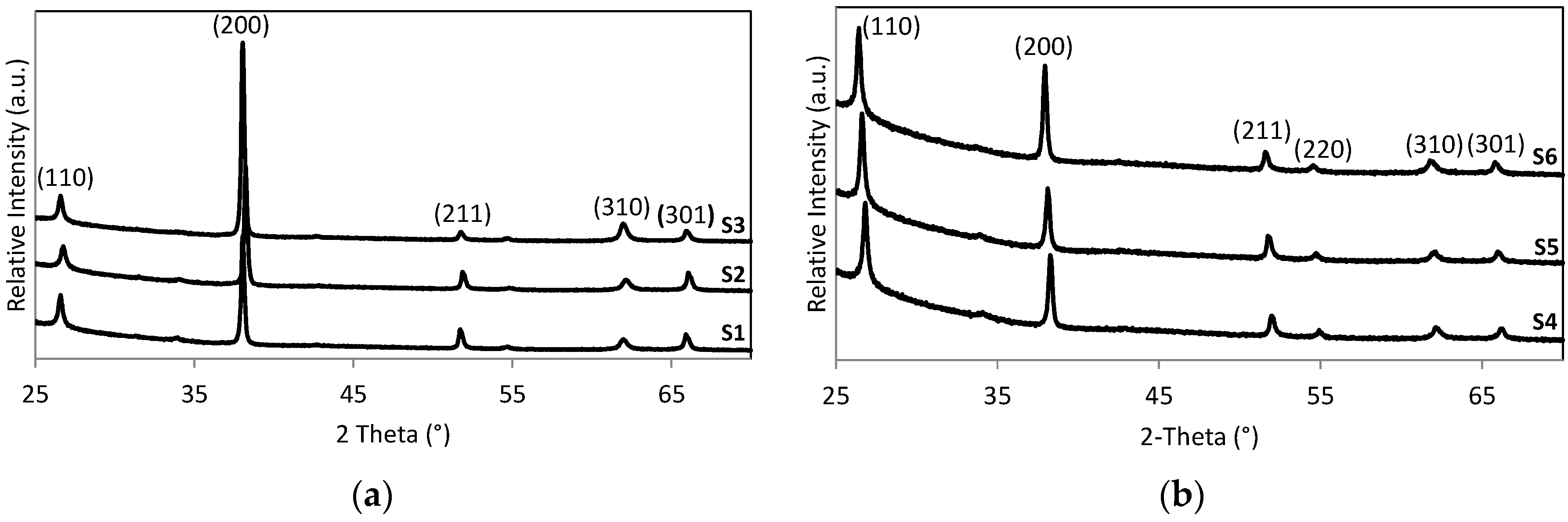
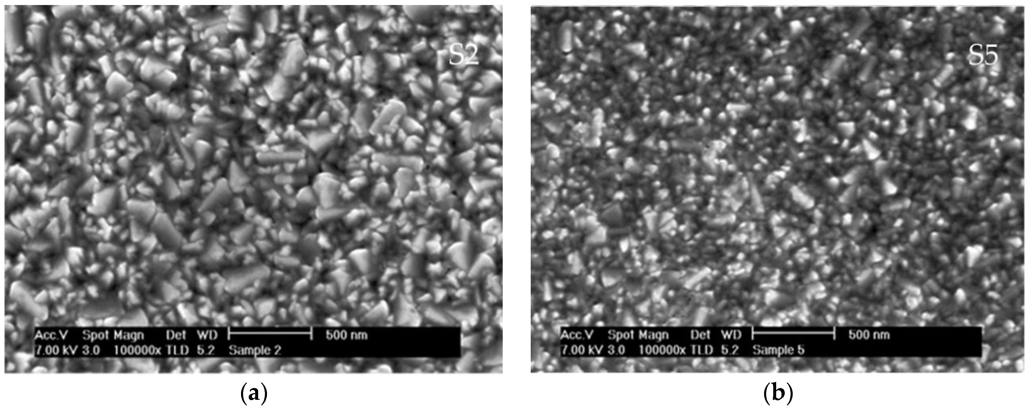
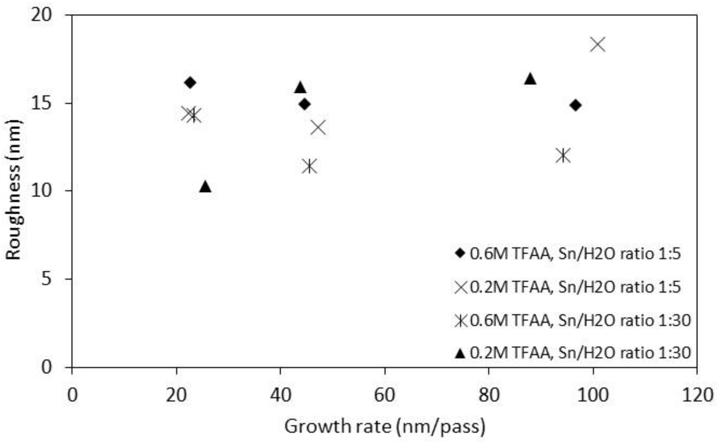
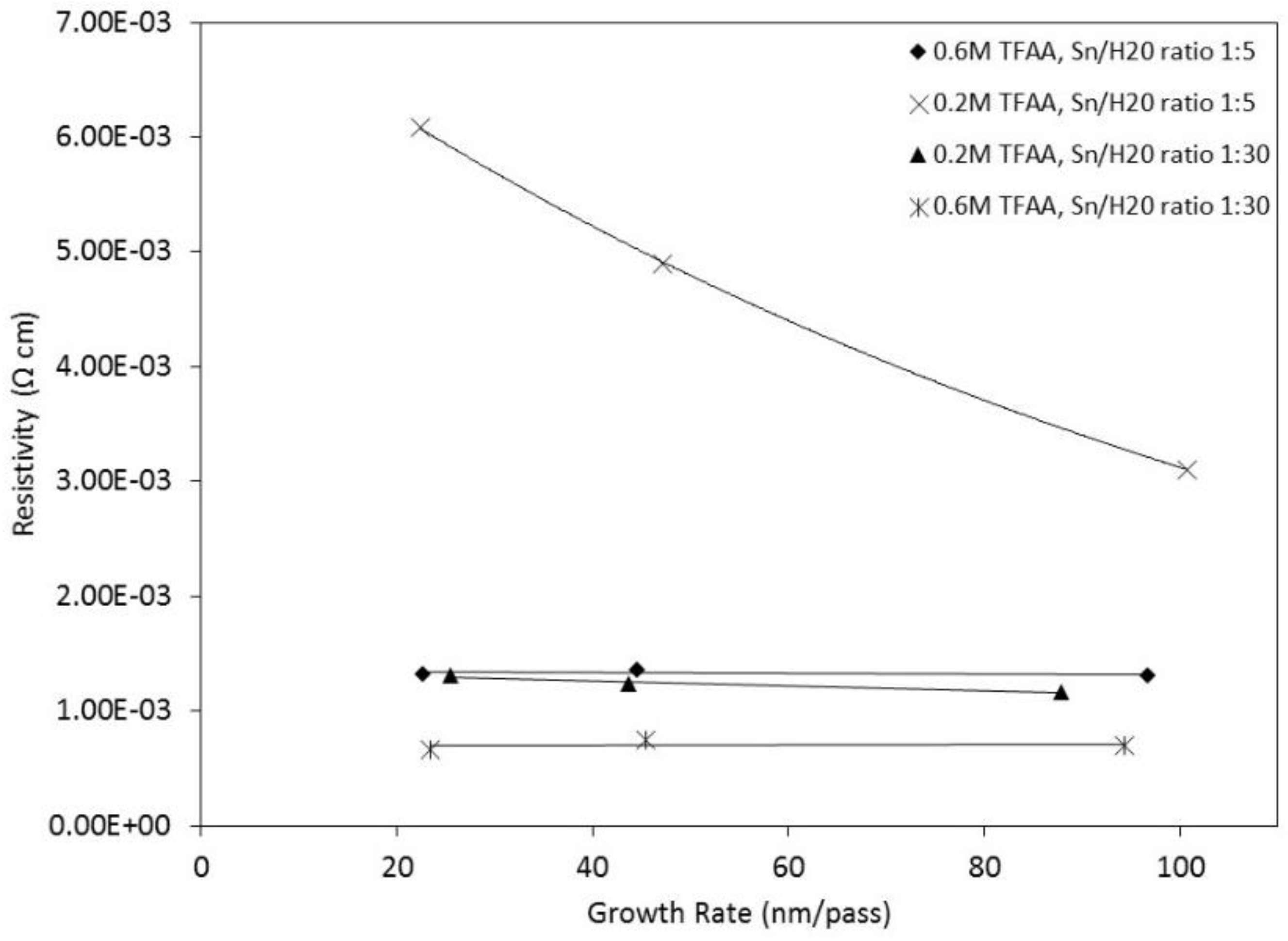
3. Results and Discussion

A considerable body of work exists on the CVD of FTO films [4,15,16] however, functional properties as a result of different translation speeds on doping levels and Sn:H2O are still missing and is the focus of the present study. The experiments concentrated on producing FTO films of similar thicknesses by controlling the number of passes under the coating head (Figure 1 and Figure S1 in the supplementary materials). This eliminates thickness associated film morphological, optical and electrical changes. Other experimental conditions were kept constant with growth temperature set at 600 °C. A summary of conditions and resulting film properties is given in Table 1.
The coatings showed good coverage, were robust under vigorous washing and could not be easily scratched. As shown in Figure 2, there is a decrease in growth rates as translation speed goes from low to high. To illustrate the point, growth rate ranges between 22 to 101 nm/pass for 0.2 M TFAA solution. This relates directly to the decrease in precursor residence time above the substrate. Samples with 30:1 water to tin precursor ratio also demonstrated a reduction in growth rates with respect to translation speeds (see Table 1). The observed growth patterns are in-line with the reported APCVD of doped ZnO thin films where reduced film thicknesses are seen at low residence times [14]. In our studies, less pronounced difference is evident in the film growth rates at different dopant levels or precursor ratios as given in Table 1.
The X-ray powder diffraction (XRPD) of S1–S6 confirmed the deposition of polycrystalline SnO2 films with tetragonal structure, without any Sn (JCPDS: 04-0673) or SnO (JCPDS: 06-0395) impurities (Figure 3). The greatest intensity signals for these would have occurred for Sn at 30.8° (200), 32.1° (200), and 44.1° (220). Neither were SnO peaks seen at 25.2° (112), 28.5° (211) or 30.8° (202). All the major peaks corresponding to (110), (101), (200), (211), (220), and (310) planes are in-line with the literature values (JCPDS: 21-1250). To our surprise, the particle size calculated using the Scherrer equation showed similar values at different growth rates and were screened from growth rate effects. For example, the particle sizes determined for S1, S2, and S3 are 37, 37, and 36 nm, respectively (Table 2). However, a reduction in TFAA concentration from 0.6 to 0.2 M decreased the average particle size from 37 to 30 nm (with a calculated standard deviation of 0.4%) (Table 2). This was corroborated by scanning electron microscope images (for S2 and S5) which confirmed particle size reduction and formation of relatively dense films (Figure 4). On close inspection, both samples also exhibited similar structural features i.e. pyramidal with textured grain boundaries. However, this is more prevalent for S2, due to large particle sizes.
Another important difference between high (S1–S3) and low dopant samples (S4–S6) is the intense (200) peak in the former. The texture coefficients (TC) calculated (using equation 2 in the experimental section) for (110), (101), (200), and (211) reflections are listed in Table 2. For the high dopant samples there appears to be a trend which shows that as the translation rate increases, the TC for (110), (101), and (211) decreases whereas it increases for (200) with respect to their translation rates. In other words, reduction in growth rates increasingly leads to preferred orientation along the (200) plane of SnO2. For the low dopant level samples (S4–S6), no such trends are seen. The TC for (110), (101), and (211) initially increased and then decreased, while TC (200) initially decreased and then increased. Irrespective of fluorine concentration, films again showed a preferred orientation along the (200) plane of tetragonal SnO2. More importantly, the TC of (200) for the higher dopant level is greater than that for the lower dopant level and is associated with an increased number of particles having a preferred orientation along the (200) directions. The prominent (200) peak in S1–S3 and the emergence of a stronger (110) peak in S4–S6 is mostly likely related to the concentration of the precursor materials used. It is known that the films with a preferred orientation of (200) require high halogen rich gases [20,21]. Under the growth conditions, the S1–S3 having a higher concentration of TFAA solution will result in more gaseous polar molecules and will adsorb on polar F-(101) surfaces. This will ultimately lead to film growth along the (200) plane, by depressing the (110) growth plane [22]. Due to limited supply of polar by-product molecules in S4–S6, fewer molecules are absorbed on the F-(101) planes and result in a moderately stronger (110) peak. In a recent study, Wang and co-workers showed that different preferred orientations of FTO films (deposited by APCVD) could be achieved using different additives and then how their properties are consequently altered [23]. It was clearly demonstrated that the films with a preferred orientation along the (200) axis are highly desired as they yield improved electrical conductivities [24].
High surface roughness is less ideal for solar performance of our target perovskite cells. The atomic force microscopy (AFM) images exhibited pyramidal type features for the films regardless of deposition conditions (Figure 5a). Different growth rates seem to have little effect on the root mean square (RMS) roughness of films deposited using the higher dopant concentration, only varying by ±2 nm. However, deposition at the lower dopant concentration level showed a small, but real decrease in roughness with decreased growth rate, as previously observed by us (Figure 6) [25]. At high H2O concentration, films in general are slightly smoother, i.e., have low RMS values and are in-line with previous reported observations [10]. Low roughness values combined with granular morphologies in deposited films are associated with the presence of (200) preferred orientation. Whereas, FTO films (deposited by spray pyrolysis technique) having pyramidal grain morphologies and large RMS values are seen for (110) preferred orientation [26]. Examples of quantified height and angle of the surface features further revealed the translation speed effects (Figure 5a,b). Samples S1–S9 demonstrated less profound variations in their height and angle distributions at different speeds, with values fairly close to each other. For high precursor ratio, low doping level samples (S10–S12), a narrowing distribution of their height and lower feature angle is more prevalent with increased translation speeds or low growth rates. However, the relative broadness of the angle distribution shows similar variation in feature shapes.
High transmission and low haze, i.e., the ability to scatter and trap light are important characteristics of enhanced light trapping properties in solar cells. It is worth noting that optical properties are highly dependent on the film thickness and roughness. Figure 7 illustrates that despite the difference in growth rates, films with average thickness of approx. 370 nm showed excellent transmittance >80% at different wavelengths and any absorption losses were minimised. The maximum transmittance was up to 89% for S6 at 650 nm. The values have also taken account of absorption and reflection from the glass substrates. The low haze values measured at 450 nm are <2%, reflecting smooth film surfaces and are consistent with AFM observations (Table 1). Measurements at other wavelengths (not shown here) showed similar haze properties. In particular for the low dopant levels, the haze reflects the changes in surface roughness; generally, the higher translation speeds giving the low haze values.
The electrical characterization carried out at room temperature, exhibited n-type character within films. Among all the films, low dopant level samples (S4–S6, 0.2 M) showed the largest variation in resistivity (p) (Figure 8) which ranged between 3.1–6.9 × 10⁻³ Ω·cm. The amount of F-dopant precursor is the same for this set of samples, so changes in p are assumed to be due to the change in translation rate and hence growth rate. The reduced growth rate results in decreased TC along the (200) preferred orientation and an increase in the (110) direction [22,23]. A reduction in (200) orientation has previously been linked by Wang et al [22] to lower conductivities. Limited change was shown in resistivity for all other sets of samples as summarized in Table 1. Hall effect data for the low dopant level films showed that the carrier concentration (N) decreased from 1.60 × 1020 cm−3 to 5.8 × 1019 cm−3 as the translation rate increased and growth rate reduced from 101 to 22 nm/pass. As evident in Table 1, improvement in the mobility (µ) is also seen for the films. These observations i.e., increased p, reduced N, and larger µ clearly point to the known scattering mechanism at the reduced grain boundaries [27,28,29] induced by changes in growth rates or high translation speeds. On the contrary, at the higher dopant level (S1–S3) showed very little change in p however, both N and µ changed considerably at different translation rates. Decreased p in the films is attributed to increased TC values along the (200) direction. Samples S7–S9 with different speeds having 0.6 M TFAA and 1:30 Sn/H2O ratio but with different speeds were significantly less resistive and showed p ranging between 6.65 × 10⁻⁴ and 7.53 × 10⁻⁴ Ω·cm. This may be a result of effective substitution of O2 by F in the SnO2 lattice [25]. Almost no difference in µ is found, but N marginally decreased from 4.70 × 10²⁰ to 3.9 × 1020 cm−3. Samples S10–S12 showed similar levels of N and µ to S7–S9 but were determined to be slightly more resistive due to the combined effects of translation speeds and dopant level. As most of N are in excess of 1020 cm−3, the scattering processes are likely to be associated with the bulk properties of the deposited films [29].

4. Conclusions

We have shown that increasing the translation rates of the susceptor results in lower growth rates and hence reduced surface roughness with smoother features. Regardless of growth parameters, films showed a preferred orientation along the (200) planes which was reduced in the case of low dopant samples, with increased prominence of the (110) planes. All films showed low optical haze and good transmission making them suitable candidates for dye and perovskite based solar cells. Electrical properties confirmed that low dopant samples became more resistant at reduced growth rates which is mainly attributed to the decreased texture coefficient value for the (200) peak.

Supplementary Materials

The following are available online at https://www.mdpi.com/2079-6412/6/3/43/s1. Figure S1: Film thicknesses at different translation speeds for (×) 0.6M and (■) 0.2M TFAA solutions using Sn/H2O ratio of (a) 1:5 and (b) 1:30.

Acknowledgments

This work was financed by Framework 7 grant FP7 NMP 2012.1.4-1 PLIANT “Process Line Implementation for Applied Surface Nanotechnologies.” The authors acknowledge Geoff Parr from Salford Analytical Services for the SEM images.

Author Contributions

Heather M. Yates and Mohammad Afzaal conceived and designed the experiments. Mohammad Afzaal and John L. Hodgkinson performed the experiments. Data analysed by all authors. Paper written by Mohammad Afzaal with the help of Heather M. Yates.

Conflicts of Interest

The authors declare no conflict of interest.

References

  1. Beneking, C.; Rech, B.; Wieder, S.; Kluth, O.; Wagner, H.; Frammelsberger, W.; Geyer, R.; Lechner, P.; Rubel, H.; Schade, H. Recent developments of silicon thin film solar cells on glass substrates. Thin Solid Films 1999, 351, 241–246. [Google Scholar] [CrossRef]
  2. Tiwari, A.N.; Khrypunov, G.; Kurdzesau, F.; Bätzner, D.L.; Romeo, A.; Zogg, H. CdTe solar cell in a novel configuration. Prog. Photovolt. Res. Appl. 2004, 12, 33–38. [Google Scholar] [CrossRef]
  3. Lewis, B.G.; Paine, D.C. Applications and processing of transparent conducting oxides. Mater. Res. Soc. Bull. 2000, 25, 22–27. [Google Scholar] [CrossRef]
  4. Edwards, P.P.; Porch, A.; Jones, M.O.; Morgan, D.V.; Perks, R.M. Basic materials physics of transparent conducting oxides. Dalton Trans. 2004, 19, 2995–3002. [Google Scholar] [CrossRef] [PubMed]
  5. Baraton, M.-I. Transparent conductive oxide materials: financial stakes and technological challenges. Int. J. Nanotech. 2009, 6, 776–784. [Google Scholar] [CrossRef]
  6. Sheel, D.W.; Yates, H.M.; Evans, P.; Dagkaldiran, U.; Gordijn, A.; Finger, F.; Remes, Z.; Vanecek, M. Atmospheric pressure chemical vapour deposition of F doped SnO2 for optimum performance solar cells. Thin Solid Films 2009, 517, 3061–3065. [Google Scholar] [CrossRef]
  7. Noor, N.; Chew, C.K.T.; Bhachu, D.S.; Waugh, M.R.; Carmalt, C.J.; Parkin, I.P. Influencing FTO thin film growth with thin seeding layers: A route to microstructural modification. J. Mater. Chem. C 2015, 3, 9359–9368. [Google Scholar] [CrossRef]
  8. Vernardou, D.; Pemble, M.E.; Sheel, D.W. In-situ Fourier transform infrared spectroscopy gas phase studies of vanadium (IV) oxide coating by atmospheric pressure chemical vapour deposition using vanadyl (IV) acetylacetonate. Thin Solid Films 2008, 516, 4502–4507. [Google Scholar] [CrossRef]
  9. Springer, J.; Poruba, A.; Vanecek, M. Improved three-dimensional optical model for thin-film silicon solar cells. J. Appl. Phys. 2004, 90, 5329–5337. [Google Scholar] [CrossRef]
  10. Yates, H.M.; Evans, P.; Sheel, D.W.; Nicolay, S.; Ding, L.; Ballif, C. High-performance tandem silicon solar cells on F:SnO2. Surf. Coat Technol. 2013, 230, 228–233. [Google Scholar] [CrossRef]
  11. Yates, H.M.; Evans, P.; Sheel, D.W.; Nicolay, S.; Ding, L.; Ballif, C. The development of high performance SnO2:F as TCOs for thin film silicon solar cells. Surf. Coat. Technol. 2012, 213, 167–174. [Google Scholar] [CrossRef]
  12. Mehmood, U.; Afzaal, M.; Al-Ahmed, A.; Yates, H.M.; Hakeem, A.S. Effect of transparent conductive oxide (TCO) film properties on the photovoltaic performance of dye-sensitized solar cells: A move towards 11% efficiency. IEEE J. Photovol. 2016. submitted. [Google Scholar]
  13. Agashe, C.; Hüpkes, J.; Schöpe, G.; Berginski, M. Physical properties of highly oriented spray-deposited fluorine-doped tin dioxide films as transparent conductor. Sol. Energy Mater. Sol. Cells 2009, 93, 1256–1262. [Google Scholar] [CrossRef]
  14. Illiberi, A.; Kniknie, B.; Deelan, J.V.; Steijvers, H.L.A.H.; Habets, D.; Simons, P.J.P.M.; Janssen, A.C.; Beckers, E.H.A. Industrial high-rate (14 nm/s) deposition of low resistive and transparent ZnOx:Al films on glass. Sol. Energy Mater. Sol. Cells 2011, 95, 1955–1959. [Google Scholar] [CrossRef]
  15. Ma, H.L.; Zhang, D.H.; Win, S.Z.; Li, S.Y.; Chen, Y.P. Electrical and optical properties of F-doped textured SnO2 films deposited by APCVD. Sol. Energy Mater. Sol. Cells 1996, 40, 371–380. [Google Scholar] [CrossRef]
  16. Ma, H.L.; Zhang, D.H.; Chen, Y.P.; Li, S.Y.; Ma, J.; Zong, F.J. Large scale fluorine doped textured transparent conducting SnO2 films deposited by APCVD. Proc. Soc. Photo. Opt. Instrum. 1996, 2897, 104–112. [Google Scholar]
  17. Yates, H.M.; Evans, P.; Sheel, D.W.; Dagkaldiran, U.; Gordijn, A.; Finger, F.; Remes, Z.; Vanecek, M. Optimum performance solar cells using atmospheric pressure chemical vapour deposition deposited TCOs. Int. J. Nanotechnol. 2009, 6, 816–827. [Google Scholar] [CrossRef]
  18. Cullity, B.D. Elements of X-ray Diffraction, 2nd ed.; Addison-Wesley: Boston, MA, USA, 1978. [Google Scholar]
  19. Barrett, C.S.; Massalski, T.B. Structure of Metals; Pergamon Press: Oxford, UK, 1980. [Google Scholar]
  20. Agashe, C.; Takwale, T.; Bhide, V.; Mahamuni, S.; Kulkarni, S.K. Effect of Sn incorporation on the growth mechanism of sprayed SnO2 films. J. Appl. Phys. 1991, 70, 7382–7386. [Google Scholar] [CrossRef]
  21. Smith, A.; Laurent, J.-M.; Smith, D.S.; Bonnet, J.-P.; Clemente, R.R. Relation between solution chemistry and morphology of SnO2-based thin films deposited by a pyrosol process. Thin Solid Films 1995, 266, 20–30. [Google Scholar] [CrossRef]
  22. Wang, J.T.; Shi, X.L.; Liu, W.W.; Zhang, X.H.; Wang, J.V.; Pyrah, L.; Sanderson, K.D.; Ramsey, P.M.; Hirata, M.; Tsuri, K. Influence of preferred orientation on the electrical conductivity of fluorine-doped tin oxide films. Sci. Rep. 2014, 4, 3679. [Google Scholar] [CrossRef] [PubMed]
  23. Wang, J.T.; Zhong, X.H.; Wang, J.N. Significant roughness enhancement of fluorine-doped tin oxide films with low resistivity and high transparency by using HNO3 addition. RSC Adv. 2015, 5, 52174–52182. [Google Scholar] [CrossRef]
  24. Yates, H.M.; Evans, P.; Sheel, D.W. The influence of F-doping in SnO2 thin films. Phys. Procedia 2013, 46, 159–166. [Google Scholar] [CrossRef]
  25. Wang, J.T.; Shi, X.L.; Zhang, X.H.; Wang, J.N.; Pyrah, L.; Sanderson, K.D.; Ramsey, P.M.; Hirata, M.; Tsuri, K. Morphology control of fluorine-doped tin oxide thin films for enhanced light trapping. Sol. Energy Mater. Sol. Cells 2015, 132, 578–588. [Google Scholar] [CrossRef]
  26. Canestraro, C.D.; Oliveira, M.M.; Valaski, R.; da Silva, M.V.S.; David, D.G.F.; Pepe, I.; da Silva, A.F.; Roman, L.S.; Persson, C. Strong inter-conduction-band absorption in heavily fluorine doped tin oxide. Appl. Surf. Sci. 2008, 255, 1874–1879. [Google Scholar] [CrossRef]
  27. Proscia, J.; Gordon, R.G. Properties of fluorine-doped tin oxide films produced by atmospheric pressure chemical vapor deposition from tetramethyltin, bromotrifluoromethane and oxygen. Thin Solid Films 1992, 214, 175–187. [Google Scholar] [CrossRef]
  28. Oshima, M.; Takemoto, Y.; Yoshino, K. Optical and electrical characterization of FTO films grown by spray pyrolysis method. Phys. Status Solidi (c) 2009, 6, 1124–1126. [Google Scholar] [CrossRef]
  29. Van den Donker, M.N.; Gordijn, A.; Stiebig, H.; Finger, F.; Rech, B.; Stannowski, B.; Bartl, R.; Hamers, E.A.G.; Schlatmann, R.; Jongerden, G.J. Flexible amorphous and microcrystalline silicon tandem solar modules in the temporary superstrate concept. Sol. Energy Mater. Sol. Cells 2007, 91, 572–580. [Google Scholar] [CrossRef]
Figure 1. A schematic illustration of a single slot coating head used for the deposition experiments.
Coatings 06 00043 g001
Figure 2. Growth rates as a function of translation speeds for films using Sn/H2O ratio of 1:5.
Coatings 06 00043 g002
Figure 3. X-ray powder diffraction (XRPD) patterns of (a) S1–S3 and (b) S4–S6.
Coatings 06 00043 g003
Figure 4. Scanning electron microscope (SEM) images of (a) S2 and (b) S5.
Coatings 06 00043 g004
Figure 5. (a) Atomic force microscopy (AFM) images and (b) statistical analysis of S10–S12.
Coatings 06 00043 g005
Figure 6. Roughness values as a function of different growth rates.
Coatings 06 00043 g006
Figure 7. Comparison of transmission values at different wavelengths (nm).
Coatings 06 00043 g007
Figure 8. Resistivity values as a function of different growth rates.
Coatings 06 00043 g008
Table 1. Effects of translation rates on resulting film properties.
Sample No.Sn/H2O RatioTFAA Concentration(M)Translation Rate (cm/min)d (μm)RMS Roughness (nm)Gr (nm/pass)p/×10−3 (Ω cm)
S11:50.6300.386 ± 0.0121596.621.31
S21:50.6700.356 ± 0.021544.541.36
S31:50.61200.361 ± 0.0261622.591.32
S41:50.2300.403 ± 0.0218100.83.1
S51:50.2700.377 ± 0.0371447.144.9
S61:50.21200.358 ± 0.0161422.386.09
S71:300.6300.377 ± 0.0151294.310.7
S81:300.6700.364 ± 0.0181145.50.65
S91:300.61200.373 ± 0.0121423.360.75
S101:300.2300.351 ±0.0251687.841.16
S111:300.2700.350 ± 0.0451643.721.24
S121:300.21200.407 ± 0.0141125.421.31
Sample No.µ (cm2/V·s)N/×1020 (cm−3)H (%) 450 nmT (%) 450 nmT (%) 531 nmT (%) 650 nmT (%) 800 nm
S1173.31.384.782.488.782.2
S2202.60.886.98487.784.2
S38.97.10.986.383.189.782.8
S4131.6283.886.585.185.2
S5210.691.184.183.988.483.9
S6190.581.286.482.289.180
S7214.70.685.283.687.581.8
S8224.20.885.483.987.183.5
S9213.90.385.781.886.982.3
S10183.31.284.984.288.882.4
S11134.71.285.384.988.282.1
S12222.3183.985.38686.9
d: Average film thickness (AFM); RMS: root mean squared; Gr: growth rate; p: resistivity; µ: mobility, N: carrier concentration; H: haze; T: transmission.
Table 2. Grain sizes and texture coefficients (TC) of films using Sn/H2O ratio of 1:5.
Sample No.Grain Size (nm)TC (110)TC (101)TC (200)TC (211)
S1370.240.023.500.24
S2370.160.023.620.20
S3360.120.013.810.06
S4290.770.062.860.31
S5300.940.072.620.38
S6300.670.043.060.23

