Article

Fullerene-Based Electron Transport Layers for Semi-Transparent MAPbBr3 Perovskite Films in Planar Perovskite Solar Cells

1
Department of Electro-optical Engineering, National Taipei University of Technology, Taipei 106, Taiwan
2
Research Center for New Generation Photovoltaics, National Central University, Taoyuan 32001, Taiwan
*
Author to whom correspondence should be addressed.
Coatings 2016, 6(4), 53; https://doi.org/10.3390/coatings6040053
Submission received: 6 September 2016 / Revised: 13 October 2016 / Accepted: 22 October 2016 / Published: 28 October 2016
(This article belongs to the Special Issue Thin Film Semiconductors for Photovoltaic Applications)

Abstract

:
In this study, four kinds of structures—[6,6]-phenyl-C61-butyric acid methyl ester (PCBM), PCBM/fullerene (C60), C60/bathocuproine (BCP), and PCBM/C60/BCP—were used as electron transport layers, and the structure, and optical and electronic behaviors of MAPbBr3 perovskite layers after annealing treatments were observed. The experimental results indicate that PCBM/C60 bi-layer structure is acceptable for MAPbBr3 planar perovskite solar cells due to electron step transporting. Low-temperature annealing is suitable for smooth and large grain MAPbBr3 films. The semi-transparent yellow C60/PCBM/MAPbBr3/PEDOT:PSS/ITO glass-structure solar cells exhibit the best performance with a power conversion efficiency of 4.19%. The solar cells are revealed to be suitable for application in building integrated photovoltaic (BIPV) systems.

1. Introduction

Perovskite solar cells (PSCs) are very impressive, with power conversion efficiencies already exceeding 20% after only a few years of development [1,2]. This rapid development can be attributed to the excellent characteristics of organometallic halide materials, primarily due to their very high absorption coefficients [3] and long carrier diffusion length [4,5]. Moreover, organometallic halide materials can be processed using solution methods requiring low-temperature steps [6]. Therefore, many deposition techniques have been developed, such as the vapor-assisted solution process [7], fast deposition-crystallization procedure [8], interdiffusion of solution-processed stacked precursor layers [9], and the two spin coating method [10].
Organometallic halide materials have been written as ABX3 (A = CH3NH3 or HC(NH2)2; B = Sn or Pb; X = I, Br or Cl), and the X-site exchange of iodide for bromide are interesting in applications in two-photon photodetectors [11] and X-ray detectors [12]. In particular, their semi-transparent behaviors are suitable for use as front cells in multi-junction photovoltaic devices [13] due to a wider band gap and higher open circuit voltage (Voc) compared to organometallic iodides. Recent studies have reported that the perovskite morphology is important to determine the performance of a final photovoltaic device [8]. Therefore, understanding of the optical, structural, and surface properties is a way to improve device performance in organometallic iodide perovskites [14,15,16,17]. To improve solar cell performance in an organometallic bromide perovskite system, a similar improvement in these material properties can be expected to be useful; however, the relationship between their fabrication processes and material properties has not been studied in detail.
Zhao et al. reported a TiO2 mesoporous PSC with a power conversion efficiency of 4.12% [18]. In this work, planar MAPbBr3 perovskites were prepared using a solution-based spin-coating process on PEDOT:PSS-coated ITO substrates to fabricate PSCs as an inverted architecture, which is a low-cost and low-temperature processed device structure when compared with conventional TiO2 mesoporous PSCs. This study investigated the optical, structural, and surface properties of MAPbBr3 perovskite films as a function of different thermal annealing temperatures. Here, four kinds of structures—[6,6]-phenyl-C61-butyric acid methyl ester (PCBM), PCBM/fullerene (C60), C60/bathocuproine (BCP), and PCBM/C60/BCP—were used as electron transport layers. C60 is a spherical fullerene molecule and PCBM is a fullerene derivative. Both are electron-transporting materials with high electron mobility. The relationship between PSC performance and the corresponding properties of the perovskite films is discussed.

2. Materials and Methods

In this study, PEDOT:PSS (AI 4083) was spin-coated on a patterned ITO substrate at 5000 rpm for 30 s, and was then annealed at 140 °C for 10 min on a hot plate. The perovskite layers were deposited using the methods described in our previous report [19]. Methylammonium bromide (MABr, 1 mmol, 112 mg) and PbBr2 (1 mmol, 376 mg) were dissolved in 1 mL of co-solvent, the volume ratio of dimethyl sulfoxide (DMSO) and γ-butyrolactone (GBL) was 1:1, and served as a MAPbBr3 precursor solution. The perovskite precursor solutions were then coated onto the PEDOT:PSS/ITO substrate using two consecutive spin-coating steps: At 1000 and 5000 rpm for 10 and 20 s, respectively. At 5000 rpm for 17 s, the wet spinning film was quenched by dropping 50 μL of anhydrous toluene into a glove box filled with nitrogen (>99.999%). After spin coating, the film was annealed at 75, 95, 115, and 135 °C for 10 min. [6,6]-phenyl-C61-butyric acid methyl ester (PCBM) was dissolved in chlorobenzene (20 mg/mL) and spin-coated onto perovskite layers at 1500 rpm for 30 s, which formed a 50-nm-thick film. C60, bathocuproine (BCP), and silver (Ag) electrodes were deposited by a thermal evaporator at thicknesses of 5 (or 50 nm on the perovskite layer), 5, and 100 nm, respectively. The BCP was used as a buffer layer for the Ag contact. The crystalline microstructure of the films was determined using a PANalytical X’Pert Pro DY2840 X-ray diffractor with Cu-Kα radiation (λ = 0.1541 nm) (PANalytical, Naerum, Denmark). A field-emission scanning electron microscope (GeminiSEM, ZEISS) was used to observe the surface morphology of the cells. Photoluminescence (PL) and absorption spectra were measured on a fluorescence spectrophotometer (Hitachi F-7000, Hitachi High-Technologies Co., Tokyo, Japan) and a UV (ultraviolet)/VIS (visible)/NIR (near infrared) Spectrophotometer (Hitachi U-4100 spectrometers, Hitachi High-Technologies Co., Tokyo, Japan), respectively. Finally, current density–voltage (JV) characteristics under irradiation by a 1000 W xenon lamp were measured using a Keithley 2420 programmable source meter. The irradiation power density on the surface of the sample was calibrated as 1000 W/m2.

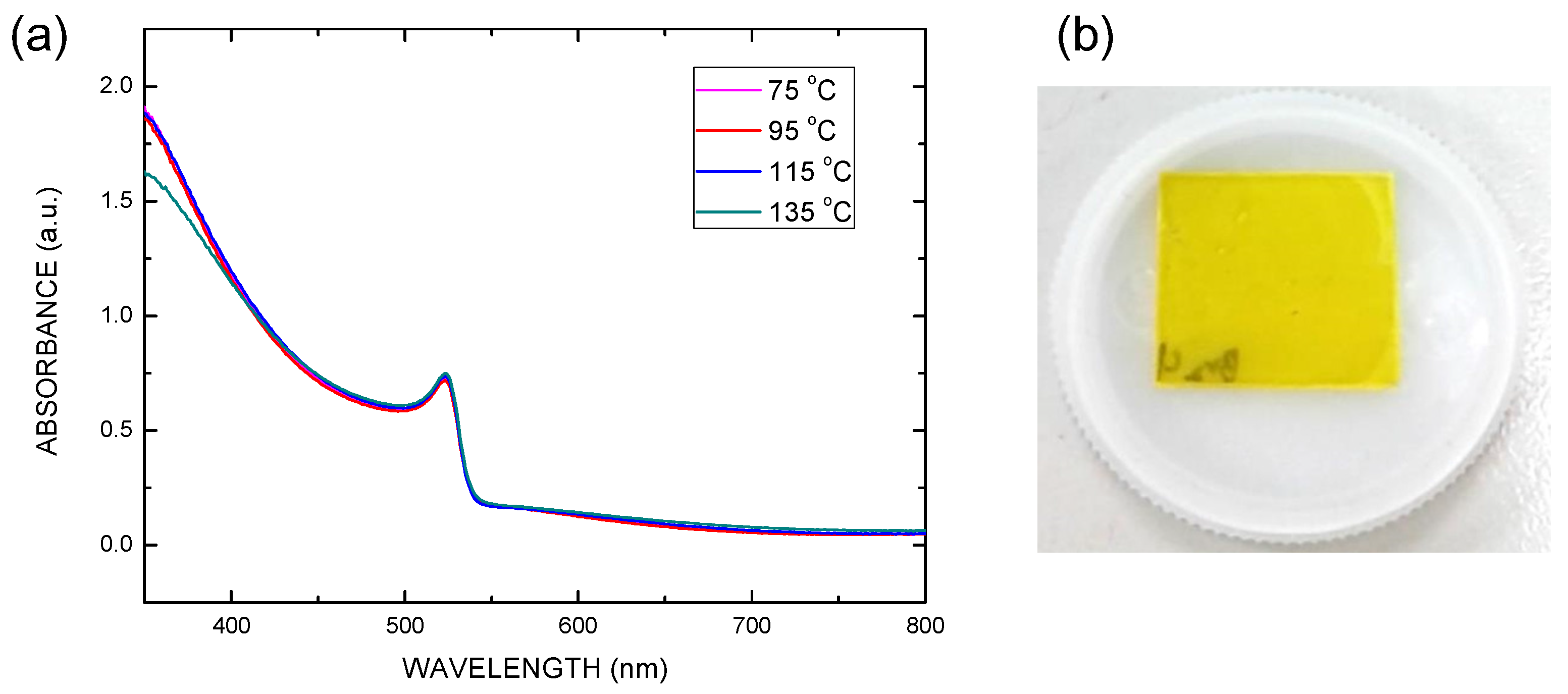
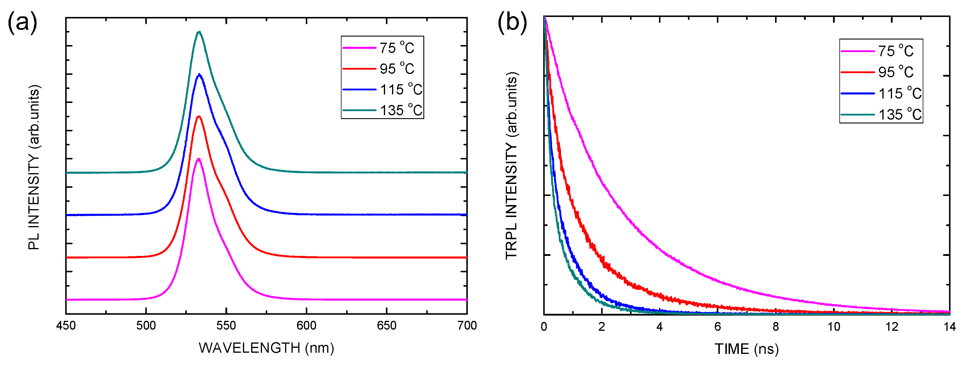
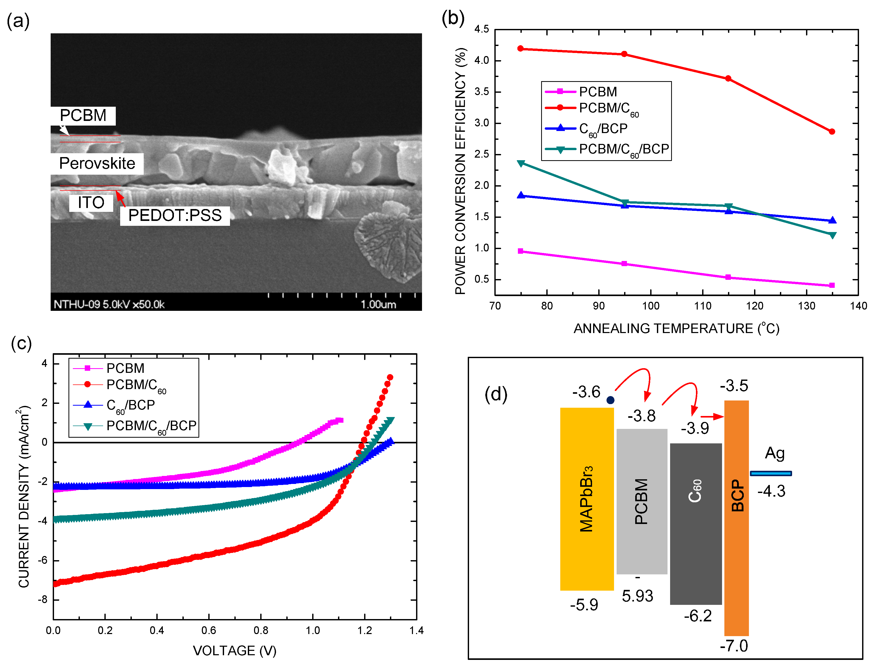
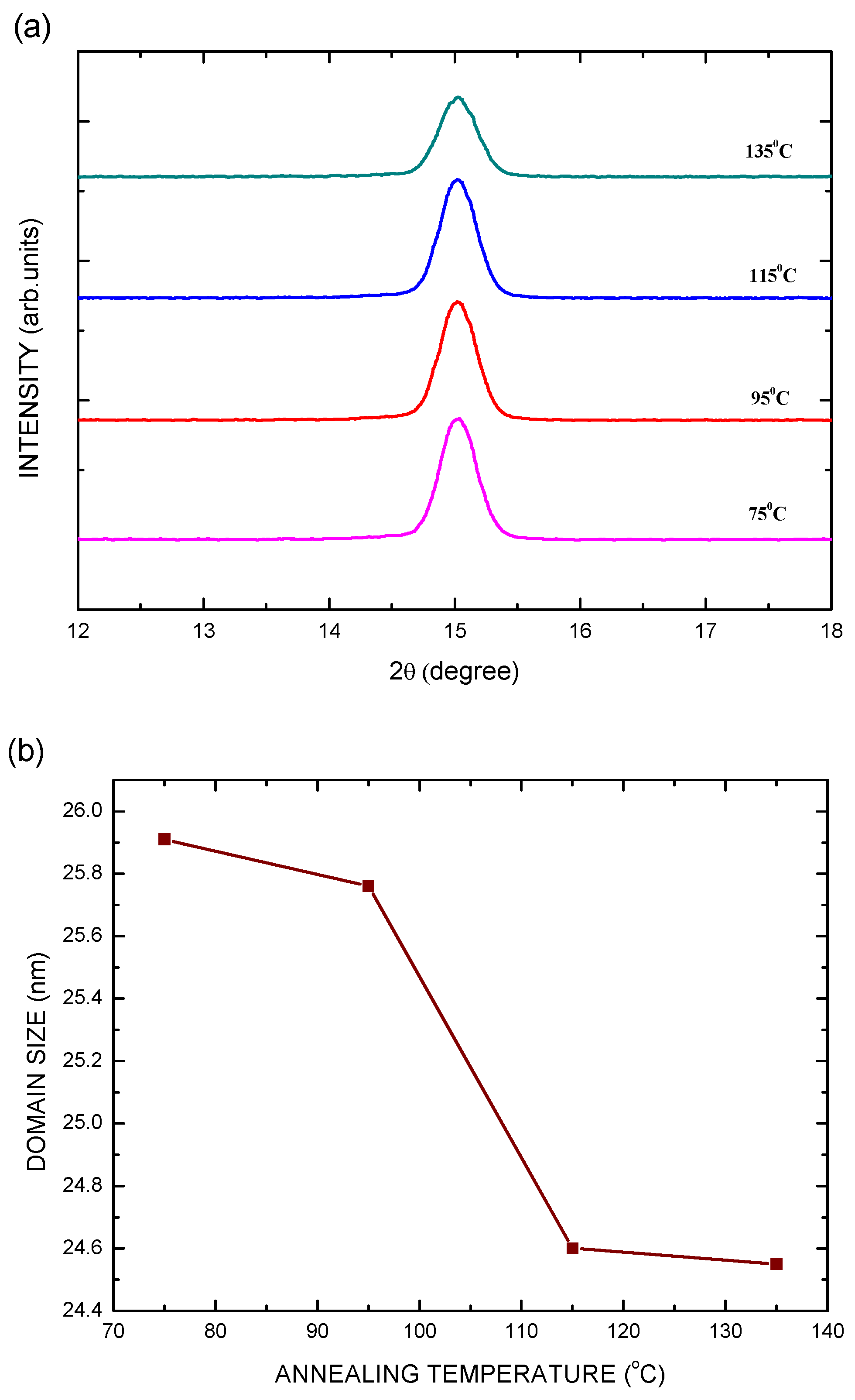
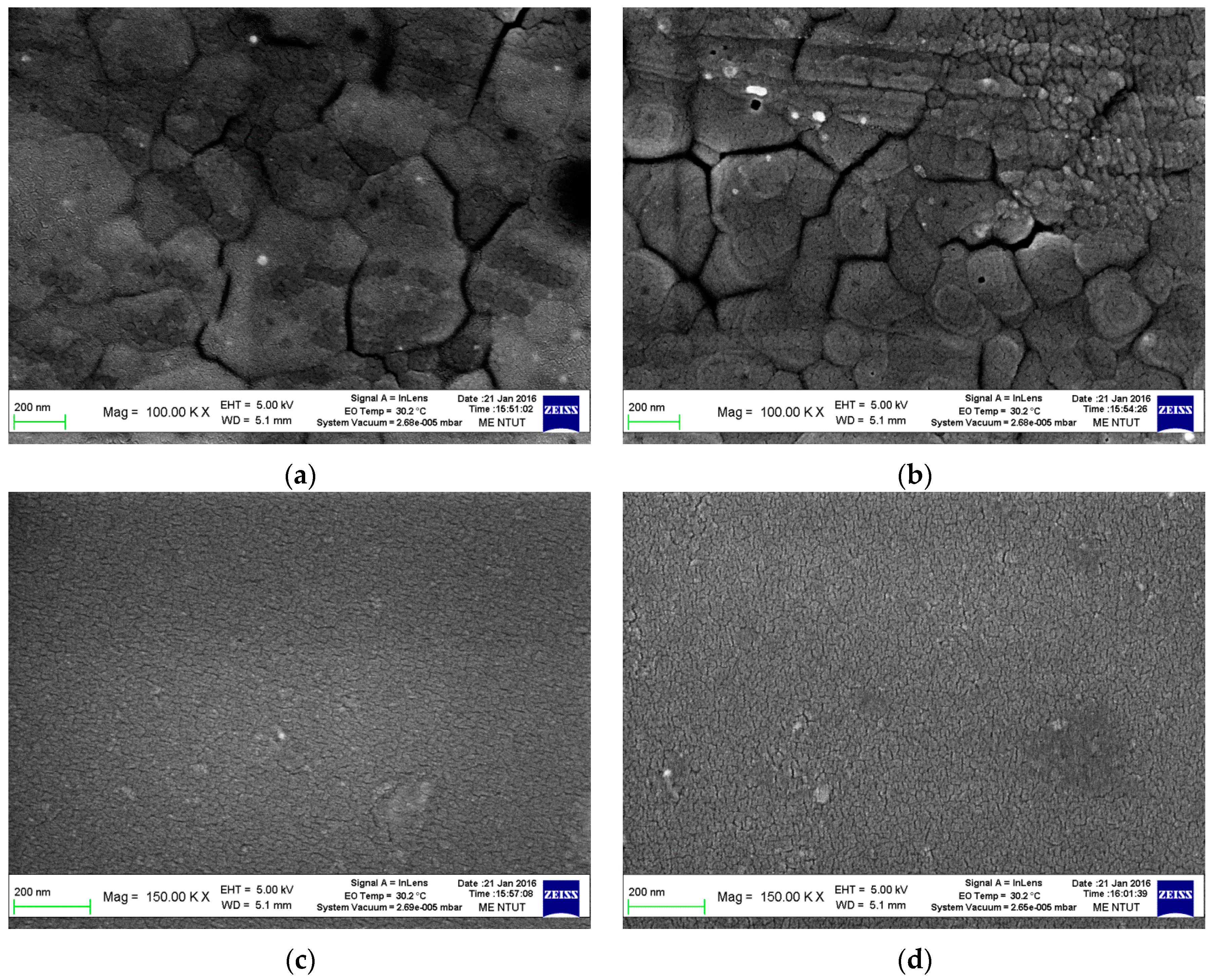
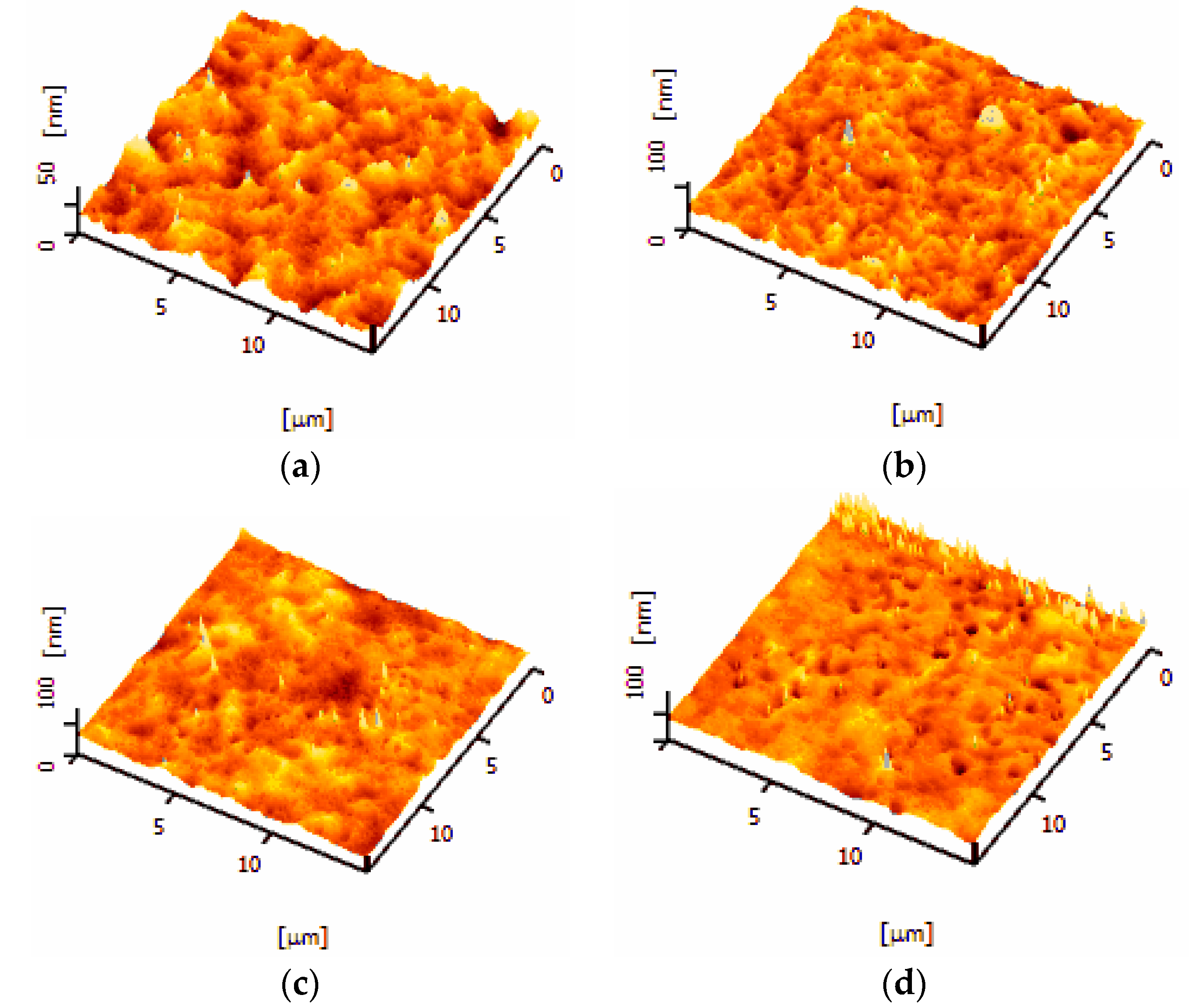
3. Results and Discussion

Figure 1a shows the X-ray diffraction (XRD) patterns of MAPbBr3 perovskite films after different thermal annealing temperatures. For each annealing temperature, the spectrum exhibits only one (001) diffraction peak at 2θ = 15.05°, which has a very strong, preferred orientation in the growth direction. When the annealing temperature increased, the full width at half maximum (FWHM) of the (001) peaks increased slightly. The smaller FWHM means a larger domain size and better crystallinity of the MAPbBr3 films. The average domain size (D) can be calculated from the FWHM of the XRD peak using Scherrer’s equation [20].
D = k λ β cos θ
where λ =1.5418 Å (X-ray diffractometer with Cu Kα radiation), β is the observed FWHM, θ is the diffraction angle of the (001) peaks, and K is a shape factor with a value of 1 for perovskite materials. The domain sizes were determined as 25.91, 25.76, 24.60, and 24.55 nm, respectively, indicating that the domain sizes decreased when the annealing temperature increased, as shown in Figure 1b.
Figure 2a shows the absorbance spectra of MAPbBr3 films after being annealed at different thermal temperatures. The absorption edges of the four perovskite films were the same, indicating that annealing temperatures cannot significantly affect the optical band gap. In fact, the band gap is mainly dependent on the ternary system composition of ABX3, or its crystal structure. The band gap in these materials is very sensitive to lattice constant variations. As an example, a band gap of Eg = 1.54 eV in MAPbI3 and Eg = 2.23 eV in MAPbBr3 are given. For a 1% reduction in lattice constants, Eg = 1.31 eV in MAPbI3 and Eg = 1.95 eV in MAPbBr3 are obtained [21]. The crystal structure of the organometallic halide, ABX3, depends on the Goldschmidt tolerance factor, t, which is relative to the radii of the constituent ions. For the compound ABX3, t is given by [21]:
t = r A + r X 2 ( r A + r X )
where rA, rB, and rX are the ionic radii of the A, B, and X ions, respectively. This factor can be used as a guide to predict the crystal structure of ABX3. On the one hand, for t = 1, an ideal cubic perovskite structure is favored. On the other hand, when the annealing temperature increased, the absorbance decreased slightly in the short-wavelength region. This may be due to the reduced domain or grain sizes after annealing treatment. Figure 2b shows an image of a typical MAPbBr3 perovskite solar cell, which clearly shows a yellow, due to the transmission of light above a wavelength of 550 nm, semi-transparent and smooth surface.
Figure 3 shows SEM images of MAPbBr3 perovskite films, thermally annealed at different temperatures. The grain size decreased significantly as the annealing temperature increased from 75 to 135 °C. The reason for this is that the MABr thermally sublimated, and PbBr2 was produced in the film surface, leading to the slight decrease in domain size, consistent with XRD data. More grain boundaries can be clearly observed when the annealing temperature is increased, which increases carrier scattering in order to reduce the mobility during carrier transport in perovskite films [22]. Smooth perovskite film is essential for fabricating photovoltaic devices with a good performance, as revealed by the atomic force microscopy (AFM) micrographs shown in Figure 4. Roughness increased significantly when the annealing temperature increased. Smooth and dense perovskite films were observed at low annealing temperatures. This indicates that low annealing temperatures are enough for producing smooth films, without defects.
Figure 5a shows the room-temperature photoluminescence (PL) spectra of MAPbBr3 perovskite films, thermally annealed at different temperatures. All films are grown on glass substrates, and the PL emission was collected from the glass substrate side in air. The PL peak was located at 532 nm, which is very close to the absorption edge (522 nm). The relatively small difference between positions of the absorption and emission spectra, which is known as the Stokes shift [23], is a sign of minor energy losses. From the PL data, a significant quenching effect was noted when the perovskite layers were treated using annealing. Thus, the annealing treatment for MAPbBr3 could lead to a PL quenching behavior. However, the PL quenching behavior is hard to accurately define. In order to further confirm these exciton behaviors, the time-resolved photoluminescence (TRPL) was measured and is shown in Figure 5b. Fitting the TRPL data with exponential decay curves establishes the lifetime of excitons and said lifetime is determined as a time constant of exponential decay. This long lifetime is essential for longer exciton diffusion lengths in order to allow large amounts of light harvesting. The corresponding lifetimes were calculated as 2.703, 1.257, 0.633, and 0.497 ns for annealing temperatures of 75, 95, 115, and 135 °C, respectively. This indicates that the strong PL emissions of samples treated at 75 °C are caused by the long exciton lifetime or the diffusion length. Low-temperature annealing is enough to improve the exciton lifetime of MAPbBr3 due to a better crystallinity.
To further confirm the material behaviors of MAPbBr3, we used Ag/PCBM/MAPbBr3/PEDOT:PSS/ITO, Ag/C60/PCBM/MAPbBr3/PEDOT:PSS/ITO, Ag/BCP/C60/MAPbBr3/PEDOT:PSS/ITO, and Ab/BCP/C60/PCBM/MAPbBr3/PEDOT:PSS/ITO glass structure photovoltaic devices to find the optimal structure and the annealing effect on MAPbBr3. Figure 6a shows a cross-sectional SEM image of the typical PCBM/MAPbBr3/PEDOT:PSS/ITO glass structure devices. Large and dense perovskite grains can be seen. Figure 6b shows the power conversion efficiency of perovskite solar cells, based on PCBM, PCBM/C60, C60/BCP, and PCBM/C60/BCP electron transport layers at different annealing temperatures. The power conversion efficiency decreases as the annealing temperature increases due to more MABr being sublimated and worse crystallinity. This indicates that high-quality MAPbBr3 films were made via a low-temperature annealing treatment. Figure 6c shows the current density–voltage (JV) plots of our best solar cells, based on PCBM/C60 electron transport layers with an annealing temperature equal to 75 °C. Table 1 lists the parameters of the perovskite solar cells, with various fullerene-based electron-transport layer structures. The optimum device exhibited an outstanding performance, with short-circuit current density = 7.23 mA/cm2, open-circuit voltage = 1.2 V, fill factor = 0.42, and a power conversion efficiency = 4.19%. The lowest unoccupied molecular orbital (LUMO) of the MAPbBr3, PCBM, and C60 films are –3.36 [24], –3.80 [25], and –3.9 [26], respectively. When the PCBM/C60 bi-layer is used as an electron transport layer, step jumping makes it easier for electrons to transport into the Ag electrode, which leads to an increased current density and open voltage, as shown in Figure 6d. Therefore, the PCBM/C60 bi-layer can reduce the energy barrier for electron transport.

4. Conclusions

To summarize, we have demonstrated the characteristics of MAPbBr3 perovskite films with thermal annealing at temperatures ranging from 75 to 135 °C. A low-temperature thermal annealing process is enough to prepare good quality MAPbBr3 perovskite films. Four layers—PCBM, PCBM/C60, C60/BCP, and PCBM/C60/BCP—were used in MAPbBr3 perovskite solar cells, and the bi-layer PCBM/C60 shows excellent behavior due to the electron step transporting path. The optimum device with a PCBM/C60 electron transport layer, annealed at 75 °C, exhibits a good performance, with a short-circuit current density = 7.23 mA/cm2, open-circuit voltage = 1.2 V, fill factor = 0.42, and a power conversion efficiency = 4.19%. The C60/PCBM/MAPbBr3/PEDOT:PSS/ITO glass structure solar cells exhibit a semi-transparent, yellow color, and are shown to be suitable in applications for building integrated photovoltaic (BIPV) systems.

Acknowledgments

Financial support for this paper was provided by the Ministry of Science and Technology of the Republic of China, under Contract no. MOST 105-2221-E-027-055.

Author Contributions

Lung-Chien Chen wrote the paper, designed the experiments, and analyzed the data. Zong-Liang Tseng, Jun-Kai Huang, Cheng-Chiang Chen, and Sheng Hsiung Chang prepared the samples and performed all the measurements. All authors read and approved the final manuscript.

Conflicts of Interest

The authors declare no conflicts of interest.

References

  1. Yang, W.S.; Noh, J.H.; Jeon, N.J.; Kim, Y.C.; Ryu, S.; Seo, J.; Seok, S.I. High-performance photovoltaic perovskite layers fabricated through intramolecular exchange. Science 2015, 348, 1234–1237. [Google Scholar] [CrossRef] [PubMed]
  2. Jeon, N.J.; Noh, J.H.; Yang, W.S.; Kim, Y.C.; Ryu, S.; Seo, J.; Seok, S.I. Compositional engineering of perovskite materials for high-performance solar cells. Nature 2015, 517, 476–480. [Google Scholar] [CrossRef] [PubMed]
  3. De Wolf, S.; Holovsky, J.; Moon, S.-J.; Löper, P.; Niesen, B.; Ledinsky, M.; Haug, F.-J.; Yum, J.-H.; Ballif, C. Organometallic Halide Perovskites: Sharp Optical Absorption Edge and Its Relation to Photovoltaic Performance. J. Phys. Chem. Lett. 2014, 5, 1035–1039. [Google Scholar] [CrossRef] [PubMed]
  4. Stranks, S.D.; Eperon, G.E.; Grancini, G.; Menelaou, C.; Alcocer, M.J.P.; Leijtens, T.; Herz, L.M.; Petrozza, A.; Snaith, H.J. Electron-Hole Diffusion Lengths Exceeding 1 Micrometer in an Organometal Trihalide Perovskite Absorber. Science 2013, 342, 341–344. [Google Scholar] [CrossRef] [PubMed]
  5. Xing, G.; Mathews, N.; Sun, S.; Lim, S.S.; Lam, Y.M.; Grätzel, M.; Mhaisalkar, S.; Sum, T.C. Long-Range Balanced Electron- and Hole-Transport Lengths in Organic-Inorganic CH3NH3PbI3. Science 2013, 342, 344–347. [Google Scholar] [CrossRef] [PubMed]
  6. Liu, D.; Kelly, T.L. Perovskite solar cells with a planar heterojunction structure prepared using room-temperature solution processing techniques. Nat. Photonics 2014, 8, 133–138. [Google Scholar] [CrossRef]
  7. Chen, Q.; Zhou, H.; Hong, Z.; Luo, S.; Duan, H.-S.; Wang, H.-H.; Liu, Y.; Li, G.; Yang, Y. Planar Heterojunction Perovskite Solar Cells via Vapor-Assisted Solution Process. J. Am. Chem. Soc. 2014, 136, 622–625. [Google Scholar] [CrossRef] [PubMed]
  8. Xiao, M.; Huang, F.; Huang, W.; Dkhissi, Y.; Zhu, Y.; Etheridge, J.; Gray-Weale, A.; Bach, U.; Cheng, Y.-B.; Spiccia, L. A Fast Deposition-Crystallization Procedure for Highly Efficient Lead Iodide Perovskite Thin-Film Solar Cells. Angew. Chem. 2014, 126, 10056–10061. [Google Scholar] [CrossRef]
  9. Xiao, Z.; Bi, C.; Shao, Y.; Dong, Q.; Wang, Q.; Yuan, Y.; Wang, C.; Gao, Y.; Huang, J. Efficient, high yield perovskite photovoltaic devices grown by interdiffusion of solution-processed precursor stacking layers. Energy Environ. Sci. 2014, 7, 2619–2623. [Google Scholar] [CrossRef]
  10. Tseng, Z.-L.; Chiang, C.-H.; Wu, C.-G. Surface Engineering of ZnO Thin Film for High Efficiency Planar Perovskite Solar Cells. Sci. Rep. 2015, 5, 13211. [Google Scholar] [CrossRef] [PubMed]
  11. Walters, G.; Sutherland, B.R.; Hoogland, S.; Shi, D.; Comin, R.; Sellan, D.P.; Bakr, O.M.; Sargent, E.H. Two-Photon Absorption in Organometallic Bromide Perovskites. ACS Nano 2015, 9, 9340–9346. [Google Scholar] [CrossRef] [PubMed]
  12. Wei, H.; Fang, Y.; Mulligan, P.; Chuirazzi, W.; Fang, H.-H.; Wang, C.; Ecker, B.R.; Gao, Y.; Loi, M.A.; Cao, L.; et al. Sensitive X-ray detectors made of methylammonium lead tribromide perovskite single crystals. Nat. Photonics 2016, 10, 333–339. [Google Scholar] [CrossRef]
  13. Heo, J.H.; Im, S.H. CH3NH3PbBr3–CH3NH3PbI3 Perovskite–Perovskite Tandem Solar Cells with Exceeding 2.2 V Open Circuit Voltage. Adv. Mater. 2016, 28, 5121–5125. [Google Scholar] [CrossRef] [PubMed]
  14. Im, J.-H.; Jang, I.-H.; Pellet, N.; Grätzel, M.; Park, N.-G. Growth of CH3NH3PbI3 cuboids with controlled size for high-efficiency perovskite solar cells. Nat. Nano 2014, 9, 927–932. [Google Scholar] [CrossRef] [PubMed]
  15. Li, W.; Fan, J.; Li, J.; Mai, Y.; Wang, L. Controllable Grain Morphology of Perovskite Absorber Film by Molecular Self-Assembly toward Efficient Solar Cell Exceeding 17%. J. Am. Chem. Soc. 2015, 137, 10399–10405. [Google Scholar] [CrossRef] [PubMed]
  16. Jeon, N.J.; Noh, J.H.; Kim, Y.C.; Yang, W.S.; Ryu, S.; Seok, S.I. Solvent engineering for high-performance inorganic–organic hybrid perovskite solar cells. Nat. Mater. 2014, 13, 897–903. [Google Scholar] [CrossRef] [PubMed]
  17. Ahn, N.; Son, D.-Y.; Jang, I.-H.; Kang, S.M.; Choi, M.; Park, N.-G. Highly Reproducible Perovskite Solar Cells with Average Efficiency of 18.3% and Best Efficiency of 19.7% Fabricated via Lewis Base Adduct of Lead (II) Iodide. J. Am. Chem. Soc. 2015, 137, 8696–8699. [Google Scholar] [CrossRef] [PubMed]
  18. Zhao, Y.; Nardes, A.M.; Zhu, K. Mesoporous perovskite solar cells: material composition, charge-carrier dynamics, and device characteristics. Faraday Discuss. 2014, 176, 301–312. [Google Scholar] [CrossRef] [PubMed]
  19. Chen, L.-C.; Chen, C.-C.; Chen, J.-C.; Wu, C.-G. Annealing effects on high-performance CH3NH3PbI3 perovskite solar cells prepared by solution-process. Solar Energy 2015, 122, 1047–1051. [Google Scholar] [CrossRef]
  20. Zhang, Z.; Wang, C.-C.; Zakaria, R.; Ying, J.Y. Role of Particle Size in Nanocrystalline TiO2-Based Photocatalysts. J. Phys. Chem. B 1998, 102, 10871–10878. [Google Scholar] [CrossRef]
  21. Jishi, R.A. Modified Becke-Johnson exchange potential: Improved modeling of lead halides for solar cell applications. AIMS Mater. Sci. 2016, 3, 149–159. [Google Scholar] [CrossRef]
  22. Brandt, R.E.; Stevanović, V.; Ginley, D.S.; Buonassisi, T. Identifying defect-tolerant semiconductors with high minority-carrier lifetimes: beyond hybrid lead halide perovskites. MRS Commun. 2015, 5, 265–275. [Google Scholar] [CrossRef]
  23. Zhang, M.; Yu, H.; Lyu, M.; Wang, Q.; Yun, J.-H.; Wang, L. Composition-dependent photoluminescence intensity and prolonged recombination lifetime of perovskite CH3NH3PbBr3-xClx films. Chem. Commun. 2014, 50, 11727–11730. [Google Scholar] [CrossRef] [PubMed]
  24. Yan, J.; Saunders, B.R. Third-generation solar cells: a review and comparison of polymer: Fullerene, hybrid polymer and perovskite solar cells. RSC Adv. 2014, 4, 43286–43314. [Google Scholar] [CrossRef]
  25. Li, Z.; Dong, Q.; Li, Y.; Xu, B.; Deng, M.; Pei, J.; Zhang, J.; Chen, F.; Wen, S.; Gao, Y.; et al. Design and synthesis of solution processable small molecules towards high photovoltaic performance. J. Mater. Chem. 2011, 21, 2159–2168. [Google Scholar] [CrossRef]
  26. Schueppel, R.; Schmidt, K.; Uhrich, C.; Schulze, K.; Wynands, D.; Brédas, J.L.; Brier, E.; Reinold, E.; Bu, H.B.; Baeuerle, P.; et al. Optimizing organic photovoltaics using tailored heterojunctions: A photoinduced absorption study of oligothiophenes with low band gaps. Phys. Rev. B 2008, 77, 085311. [Google Scholar] [CrossRef]
Figure 1. (a) X-ray diffraction (XRD) patterns of MAPbBr3 perovskite films treated at different annealing temperatures; (b) Relationship between domain size and annealing temperature.
Coatings 06 00053 g001
Figure 2. (a) Absorbance spectra of MAPbBr3 perovskite films after different thermal annealing temperatures; (b) Photograph of the MAPbBr3 perovskite solar cell without electrodes.
Coatings 06 00053 g002
Figure 3. SEM images of MAPbBr3 perovskite films treated at different annealing temperatures: (a) 75 °C; (b) 95 °C; (c) 115 °C; (d) 135 °C.
Coatings 06 00053 g003
Figure 4. Atomic force microscopy (AFM) images of MAPbBr3 perovskite films treated at different annealing temperatures: (a) 75 °C; (b) 95 °C; (c) 115 °C; (d) 135 °C.
Coatings 06 00053 g004
Figure 5. (a) Photoluminescence (PL) and (b) time-resolved photoluminescence (TRPL) of the perovskite films treated at different annealing temperatures.
Coatings 06 00053 g005
Figure 6. (a) Cross-sectional SEM images of the C60/PCBM/MAPbBr3/PEDOT:PSS/ITO glass structure; (b) Power conversion efficiency as a function of annealing temperatures for four electron transport layer structures; (c) The current density–voltage (JV) curves of the best perovskite solar cells of the four electron transport layer structures; (d) Corresponding energy band diagram in this study.
Coatings 06 00053 g006
Table 1. Parameters of perovskite solar cells with various fullerene-based electron transport layer structures.
Electron Transporting LayerJsc (mA/cm2)Voc (V)FFPCE (%)
PCBM2.440.950.410.95
PCBM/C607.231.20.424.19
C60/BCP2.271.290.631.84
PCBM/C60/BCP3.881.230.502.37

