Article

Evolution of Nanostructure and Metastable Phases at the Surface of a HCPEB-Treated WC-6% Co Hard Alloy with Increasing Irradiation Pulse Numbers

1
School of Materials Science and Engineering, Shenyang University of Technology, Shenyang 110870, China
2
Key Laboratory of Materials Modification & School of Materials Science and Engineering, Dalian University of Technology, Dalian 116024, China
3
College of Materials Science and Engineering, Liaoning Technical University, Fuxin 123000, China
4
Laboratoire d’Etude des Microstructures et de Mécanique des Matériaux (LEM3), Université de Lorraine, CNRS UMR 7239, Ile du Saulcy, 57045 Metz, France
*
Authors to whom correspondence should be addressed.
Coatings 2017, 7(11), 178; https://doi.org/10.3390/coatings7110178
Submission received: 30 July 2017 / Revised: 7 October 2017 / Accepted: 17 October 2017 / Published: 26 October 2017

Abstract

:
This work investigates the mechanisms of the microstructure evolution in the melted surface layers of a WC-6% Co hard alloy when increasing the number of pulses of irradiation by high-current pulsed electron beam (HCPEB) treatment. After one pulse of irradiation, about 50% of the stable hcp WC phase was melted and resolidified into the metastable fcc form (WC1−x). When increasing the numbers of pulse irradiation, the WC phase decomposed into ultrafine-grained WC1−x plus nanosized graphite under our selected energy condition. Because of the rapidity of HCPEB carried under vacuum, the formation of the brittle W2C phase was avoided. In the initial Co-rich areas, where the Co was evaporated, melting and solidification led to the formation of nanostructures Co3W9C4 and Co3W3C. The volume fraction of the nano domains containing WC1−x, Co3W9C4, and Co3W3C phases reached its maximum after 20 pulses of irradiation. The improved properties after 20 pulses are therefore due to the presence of nano graphite that served as lubricant and dramatically decreased the friction coefficient, while the ultrafine-grained carbides and the nano domains contribute to the improvement of the surface microhardness and wear resistance.

1. Introduction

Recently, the application of energetic beams such as ion, electron, laser, and plasma has been of increasing interest as a means to modify the surface of metallic materials [1,2,3,4,5]. Compared with continuous high-power beams, pulsed beam high-power systems have attracted more and more attention for surface treatment. Among these pulsed beam techniques, the high-current pulsed electron beam (HCPEB) is relatively new [3,6] and exhibits substantial advantages in terms of simplicity, efficiency, reliability, relatively low cost, etc. Under HCPEB irradiation, the beam energy (~J/cm2) transfers into the surface layer (~μm) of material within a short pulse (~μs), leading to extremely fast heating or melting followed by rapid solidification (~107~9 K/s) [3,6,7]. As a result, non-equilibrium microstructures can be obtained. This generally leads to the formation of a surface layer with improved physical, chemical, and mechanical properties that are often unattainable with conventional surface treatment techniques [7,8,9,10].
Tungsten carbides are widely used for the fabrication of cutting tools, molds, and bearing parts due to their excellent mechanical properties. However, with the development of modern industry, there is an increasing demand for tungsten carbides working under high-temperature and high-speed abrasive and wear conditions. Various surface treatments including pulsed electron beam have accordingly been used for the surface modification of tungsten carbides [3,11,12,13,14,15,16,17,18]. Especially for the WC-Co system materials, HCPEB treatment was demonstrated to be an efficient method to improve the surface microhardness and wear resistance [12,13,16,17,18]. In particular, our earlier work that investigated the effect of the irradiation pulse numbers on the surface properties [17] revealed that an optimum wear resistance was obtained after 20 pulses of HCPEB under 27 keV. A detailed microstructure analysis has revealed that under our optimum selected condition of 20 pulses (for which the energy of the HCPEB was kept sufficiently low to avoid large stress-induced cracks), the presence of nano-scale graphite served as a solid-state lubricant [18]. The nano-scale graphite was formed as a result of the peritectic decompositions of WC carbide at high temperature non-equilibrium condition followed by a rapid solidification under HCPEB [18]. For this decomposition, the use of HCPEB treatment under low energy is of particular interest because the treatment is carried out under vacuum and the formation of volatile CO2 is avoided [18]. Consequently, the hard and brittle phase W2C which was observed elsewhere [12,13,16] was not observed. Despite these recent developments, a detailed investigation on the structure and phase evolutions of the WC-Co alloys with increasing pulses of HCPEB irradiation is still missing. This is of special interest because the surface microstructure modification occurs under non-equilibrium conditions, and previous works have already shown that the final structures and surface properties of HCPEB-treated alloys are not only dependent on electron beam energy, but also on the number of pulses [19,20,21]. In addition, as HCPEB is a thermal energy deposition process, the evolution of the structure state when refractory metals and relatively low melting point metals are combined is another interesting challenge that has received little attention. The purpose of the present work is therefore to study the effect of HCPEB pulse numbers on the microstructure and phase transformations in the surface melted layer of a WC-6% Co hard alloy.

2. Materials and Methods

The samples of size φ15 mm × 5 mm were directly bought from a hard alloy factory (Zhuzhou Cemented Carbide Group Co., Ltd., Zhuzhou, China) with product name YG6. The chemical composition (wt %) is Co ~6% and WC in balance. Figure 1 gives different images of the untreated materials under electron backscattered diffraction (EBSD) and transmission electron microscopy (TEM), respectively.
Figure 1a is an EBSD phase map showing that the WC carbide has a prismatic shape and a size ranging from 1.2 to 5 µm. WC was sintered by equilibrium hexagonal close-packed (hcp) structures, while the green areas between the red WC blocks are indicated as Co. This Co + WC mixture is better seen in the TEM bright field image in Figure 1c, where the WC is prism-like blocks having sharp angles. Figure 1b is an EBSD orientation map of the same area as shown in Figure 1a; it is revealed that each WC block corresponds to a single grain and that the orientation differences existing in the large WC particles are very small.
The HCPEB irradiation was carried out with a self-design HOPE-I-type HCPEB apparatus, which is an upgraded version of the type Nadezhda-2 by optimizing the production of anode plasma and the design of the high-voltage switch [3,22]. The typical parameters of HOPE-I are accelerating voltage 20–30 kV, peak current ~10 kA, pulse duration 0.5–5 µs, beam diameter ~40 mm, and energy density 1–10 J/cm2. In the present work, the previously-optimized parameters were used; i.e., working vacuum 8 × 10⁻³ Pa, accelerating voltage 27 kV, sample–anode distance 6 cm, pulse duration 2.5 µs, energy density 3 J/cm2, pulse interval 10 s, and 1–35 pulses. Before the HCPEB irradiation, all the samples were ground, polished, and ultrasonically cleaned in acetone.
The phase structure of modified surface was examined by glancing-angle X-ray diffraction (GAXRD) on a D/max3A diffractometer (Brucker Co., Elk Grove Village, IL, USA) operating with CuKα radiation and an incident angle fixed at 1°. The surface microstructure was observed using a Jeol-6500 field emission gun (FEG) scanning electron microscope SEM (JEOL Ltd., Akishima, Japan), to which was attached with a FEI EBSD microscope. A Hikari TSL-OIM 6.0 EBSD microscope (EDAX, energy dispersive x-ray analysis, Ametek Inc., Berwyn, PA, USA) was also used. TEM was conducted on an FEI Tecnai G2 high-resolution appendices (FEI Co., Hillsboro, OR, USA). The thin foils for TEM were prepared by one-sided milling and subsequent ion thinning in order to be as close as possible from the top surface within the melted zone. The tribological property was tested using a UMT-2 type system with the following testing conditions: Si3N4 counterpart of diameter 4.4 mm, working load 30 N, dry sliding distance 7 mm, and velocity of 2 mm/s for 30 min.

3. Results

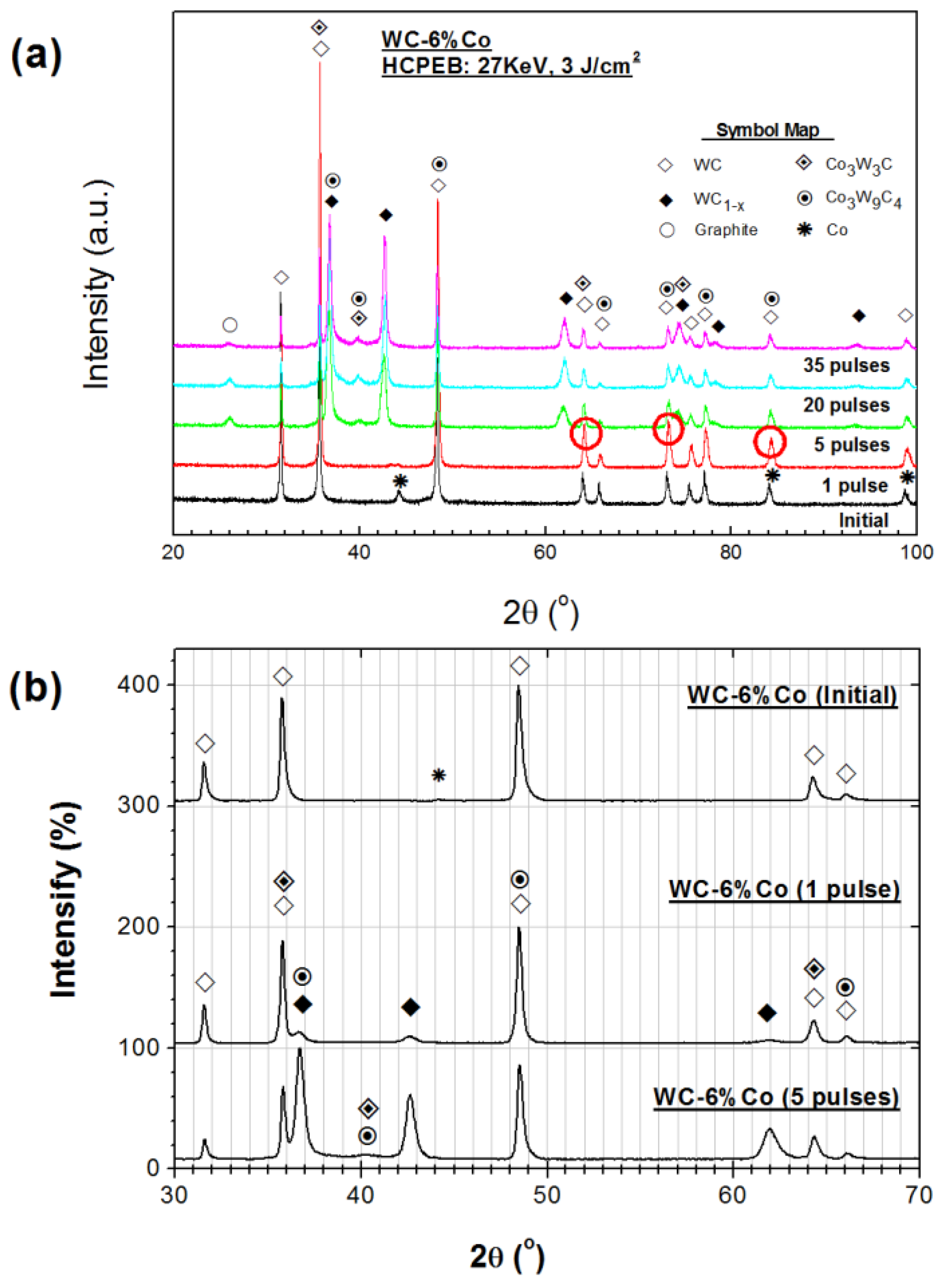
3.1. XRD Analysis of the Phases

Figure 2 shows the glancing-angle X-ray diffraction traces observed from the samples before and after the different number of HCPEB irradiation. Consistent with the analysis given in Figure 1, only the peaks corresponding to the WC (hcp) and Co (hcp) were revealed for the initial materials. After one pulse of HCPEB irradiation, the Co peaks were weakened and some WC peaks (circled in red) were intensified. The changes were related to the surface evaporation of Co and the transformation of melted Co with WC into Co3W9C4 and Co3W3C after HCPEB irradiation [17]. It is also worth noting that the WC peak splitting at around 2θ ~75° suggested the formation of the fcc WC1−x after HCPEB.
To reveal the details, fine step scanning was conducted on the samples (Figure 2b), where small peaks of the fcc WC1−x phases were detected. As the number of pulses increased, after five pulses of irradiation, the peaks of WC1−x appeared more clearly. The graphite peak was also detected at about 2θ ~26°. Upon further increasing the number of pulses to 20, the intensity of the Co3W9C4, Co3W3C, and graphite peaks slightly increased. As revealed by TEM in previous work [17,18], these graphite, WC1−x, Co3W9C4, and Co3W3C phases have a grain size distribution in the range of 20–100 nm.

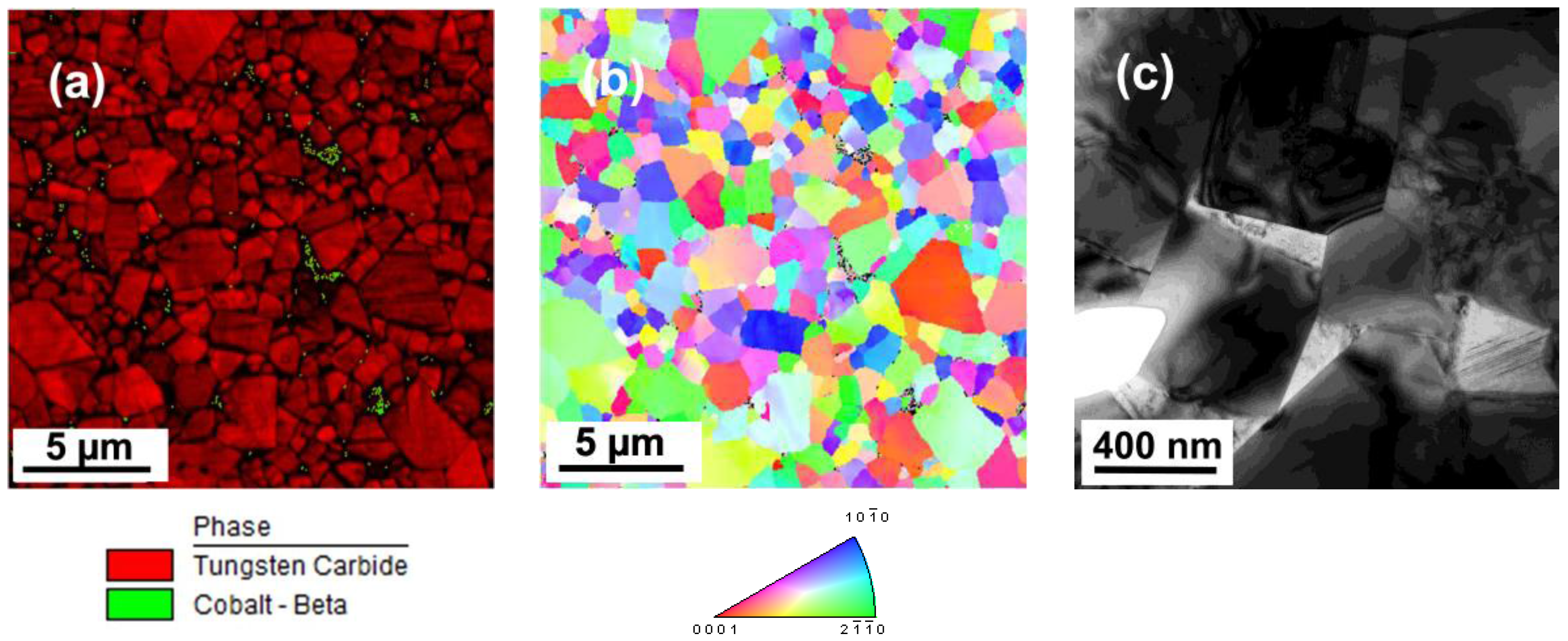
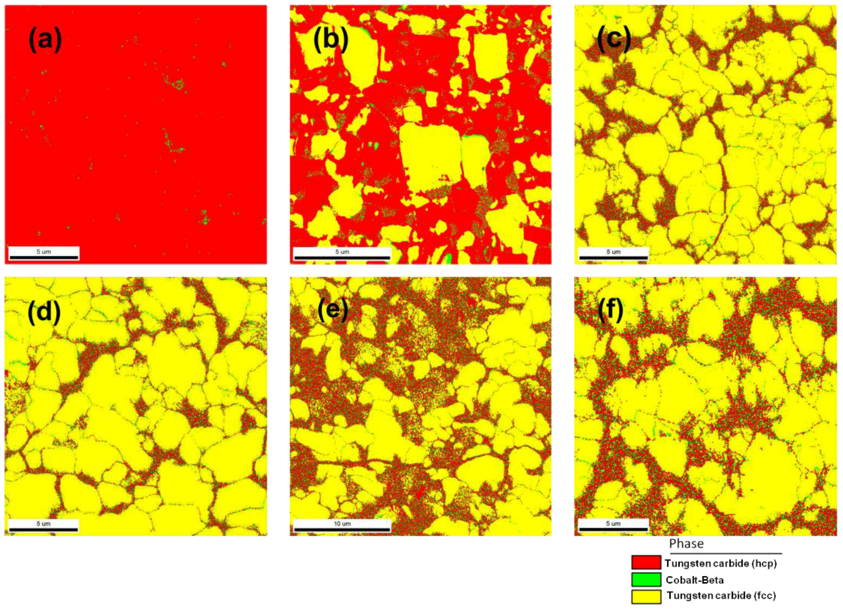
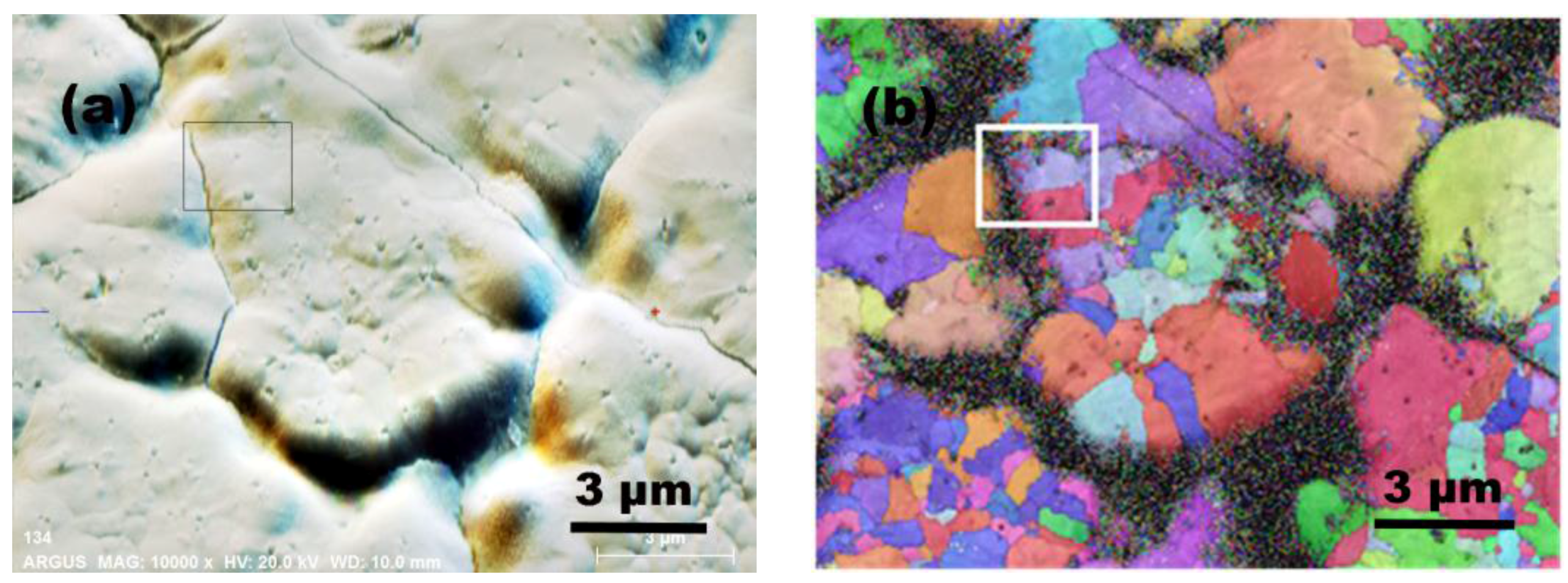
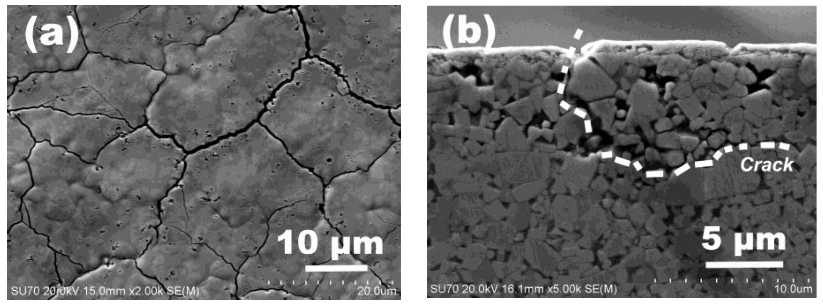
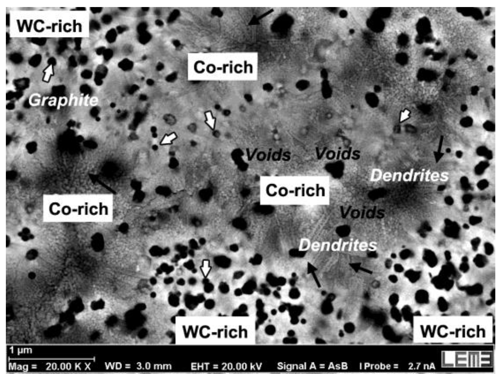
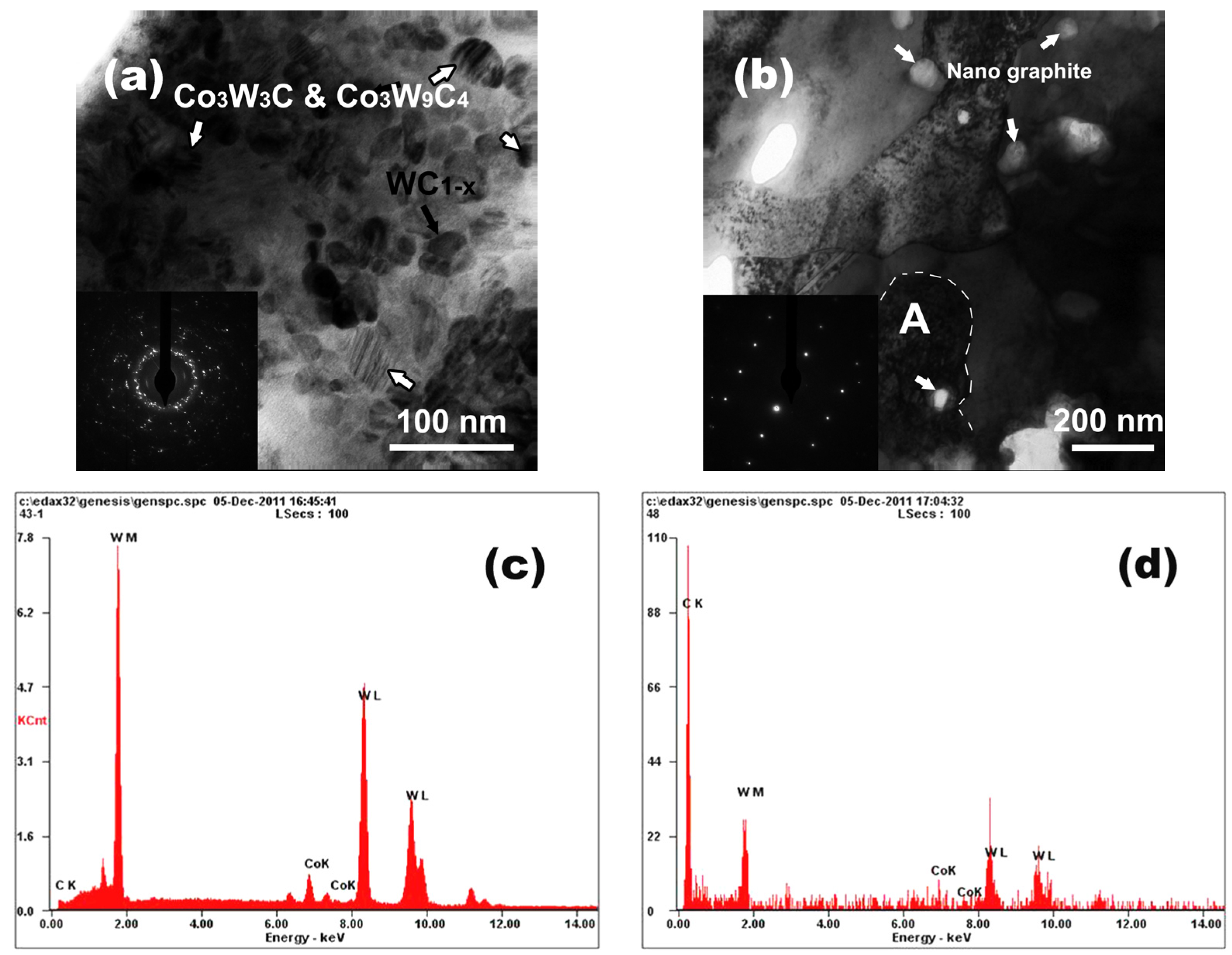
3.2. Fine Scale Microstructure Evolution Aspects with EBSD and TEM

To evaluate the evolution of those new surface nano-formations, EBSD was used on the samples irradiated with different numbers of HCPEB pulses. As shown in Figure 3a, the starting materials contained only stable WC (red) and Co (green). After one pulse of irradiation (Figure 3b), some of the WC phases changed into WC1−x (fcc) phases (in yellow). This corresponds to the XRD analysis in Figure 2. It seems that the Co phase (green) took a larger area fraction than that of the starting material after one pulse of irradiation. It is reasonable to suggest that Co got evaporated to the surface from the sub-layer under HCPEB, and with the contact melting of WC and Co at the interface, nano precipitations of Co3W9C4 and Co3W3C phases were formed as a result [14,16]. This is also consistent with the results observed in Figure 2. Since these phases have similar hcp crystal parameters to that of Co, it can be detected with the Co phase setting (green). With increasing numbers of irradiation (Figure 3c–f), WC1−x (yellow) had replaced the initial WC phase (red), while the area fraction of nano formations WC1−x (yellow), Co3W9C4, and Co3W3C (green) at the interface varied with increasing pulse numbers. Figure 4b,c proved the nano structures formation at the interface. It also needs to be noticed that the WC1−x phases in yellow islands were composed of small grains varying from several hundred nanometers to several micrometers. As compared with the starting microstructure shown in Figure 1b,c, it is obvious that the initial WC particles were divided into small pieces and gradually transformed into WC1−x (fcc) phases, while at the same time, the initial sharp angles were rounded by the heat effect of HCPEB irradiation. The arrow in Figure 4c indicated the formation of nano graphite by the peritectic decompositions, the formation and morphologies of which were observed in detail with high-magnification SEM and HRTEM in our previous work [17]. Figure 5 shows the TEM observations of the nano domains at the interface and the ultrafine grained WC1−x phases in a WC-rich area, respectively. As shown in Figure 5a, nano domains of WC1−x (20–50 nm) and nano precipitations of Co3W9C4 and Co3W3C (10–20 nm) were observed in the Co-rich area. As in the WC-rich area (Figure 5b), ultrafine grained WC1−x phases were formed accompanied with nano graphites (arrows). As discussed in the previous work, the formations were generated by the peritectic decompositions of WC at high temperature [17]. It is also interesting that—as shown in Figure 5c—the ultra-fine grain A mainly contained W by EDAX, which revealed a transformation of WC1−x → W under higher energy deposition by HCPEB; however, as observed in Figure 2, no obvious W2C were detected. This is special in the present work [11,12,15].
As discussed in a previous work [16], the nano domains played an important role on the surface mechanical properties improvement. According to Figure 3, the area fractions of nano domains at the interface were calculated with increasing number of pulses. As discussed above, the area fractions of nano domains after one pulse of irradiation were measured as that of green domains, while the others (5–35 pulses) were measured as the remaining fraction besides those yellow islands. Results are as shown in Figure 6. It is of interest that the evolution of nano domains area fractions were quite similar to the changes of surface mechanical properties reported before [16]. The area fraction of nano domains reached its highest value (~40%) after 20 pulses of irradiation. This contributed the most to the improvement of surface mechanical properties. After 35 pulses of HCPEB, the areas of nano domains decreased slightly (Figure 6), and according to Figure 3, the yellow islands composed of ultrafine-grained WC1−x seemed to combine together and have grown up a little. To verify the detailed microstructure feature, Figure 7 shows the morphologies on the surface plane and the cross-sectional plane of samples after 35 pulses of HCPEB irradiations, respectively.
As seen from Figure 7a, the surface cracks are deep and there are craters existing by the cracks. Craters are the defects of surface morphologies and properties, which usually need to be avoided [22]. As shown in Figure 7b, cracks had separated the surface melted layer and it had propagated across the depth direction to ~7–8 µm. The combination and growth of yellow WC1−x islands in Figure 3f were as a result of the crack propagating. Besides, Co evaporations from deep layers led to big holes that weaken the binding of surface melted layer with substrate. All these microstructure defects decreased the surface mechanical properties of samples irradiated after 35 pulses of HCPEB.

4. Discussion

The HCPEB bombardment gives rise to superfast heating and melting, followed by rapid solidification at the materials surface. This makes it possible to produce metastable states in the melted surface. From the results depicted in this paper, it is clear that depending on the total amount of energy transferred to the material, the aspect of the melted layer as well as its microstructure and degree of metastability were quite different (see in Figure 3). Many of those differences could be understood by considering the effect of the treatment on the dissolution kinetics of the carbides and the ability of the process to homogenize the melted surface.
Figure 8 gives the temperature and the temperature gradient variation as a function of time at different layers from the surface after a single pulse of HCPEB irradiation. According to the simulation, the surface temperature could get as high as 3200 K within 0.7 µs and then go down to ~1273 K after 4 µs. As the surface temperature is slightly higher than the melting point of tungsten carbide (~3100 K [23]), those would get partially melted at the sample surface after one pulse of HCPEB irradiation; this was proved by the previous experimental observations [17]. It is also worth noting that the surface temperature got down to ~1273 K sharply within 4 µs (seen in Figure 8a), which is much lower than the reported melting point of WC-Co (~1573 K) [23]. Considering the pulse interval (~10 s) of the present experimental setting, it suggests that the surface got enough time for cooling and solidification within a single pulse of irradiation. This conclusion is very important for the analysis of the surface metastable microstructure transformation. Further, as seen from Figure 8b, the maximum heating rate and the maximum cooling rate at the sample surface were as 4.5 × 10⁸ K/s and 1.26 × 10⁸ K/s, respectively.
As shown in Figure 9, the surface microstructure of a 20-pulsed treated sample contains two different regions: WC-rich area and Co-rich area. In the Co-rich region (Co-W-C system), nanostructures mixed with dendrites were formed. Black voids and craters were also observed in the region. Because of the large differences of heat conductivity between the tungsten carbides and the Co binder, voids were generated by the different shrinkage during the rapid solidification. The formation of craters was a result of the sublayer melt eruption as discussed elsewhere [24]. Considering the surface simulations in Figure 8, there were liquid and graphite in the surface melt at ~3200 K according to the ternary phase diagram [25], and this composite would be kept down under a rapid cooling rate of 1.26 × 10⁸ K/s. When at a relatively low temperature (~1500 K), because of the long-range chemical diffusion suppression, only the metastable phase transformation (liquid → MC(1−x) + M6C) could occur, where the MC1−x phase was suggested as WC1−x in the situation. Here it is worth noting that the MC1−x in the Co-W-C system was considered as part of the fcc interstitial [25], and the metastable transformation M6C → M12C (i.e., Co3W3C → Co3W9C4) was also reasonable during the rapid solidification. In this respect, dendrites and nano domains of WC1−x (fcc), Co3W9C4 (hcp), and Co3W3C (hcp) would get formed at the Co-rich area. At the WC-rich area, the WC decomposition occurred, and this was normally observed in the high-temperature process (~2873 K); i.e., HVOF [26,27], ion planting [28], and HCPEB [12]. However, it is usually reported in a result of W2C plus graphite mixture under an oxygen-containing environment, while in the present situation, where high vacuum was applied, the severe decomposition of WC → W2C was inhibited and instead it promoted the decomposition of WC → WC1−x without volatile CO2 formation. Therefore, in the WC-rich region, peritectic decompositions, WC → WC1−x + Graphite, of WC carbides occurred at the given parameters [17,29,30,31,32]. As a result of this, nano graphite was fabricated.
As discussed before (Figure 6), the presence of the metastable nano domains is of great importance for the improvement of surface mechanical properties of WC-Co hard alloy. The nano domains contribute to the increase of surface microhardness and the related surface wear, while at the same time, the formation of nano graphite has acted as solid lubricant and has lowered the surface friction coefficient [17].

5. Conclusions

The HCPEB technique has been applied to a WC-6% Co hard alloy to investigate the effect of the number of pulses on intriguing surface modifications—the surface microstructure evolution and phase transformations—occurring in the melted layer. The main results are summarized as follows:
  • Nano domains composed of WC1−x (fcc), Co3W9C4 (hcp), and Co3W3C (hcp) were formed at the interface and Co-rich area after HCPEB irradiations. The formation and area fraction evolution of which mainly contributed to the surface mechanical properties improvement;
  • Nano graphite as well as ultrafine-grained WC1−x (fcc) were formed in the WC-rich area after HCPEB, the formation of which decreased the surface friction coefficient;
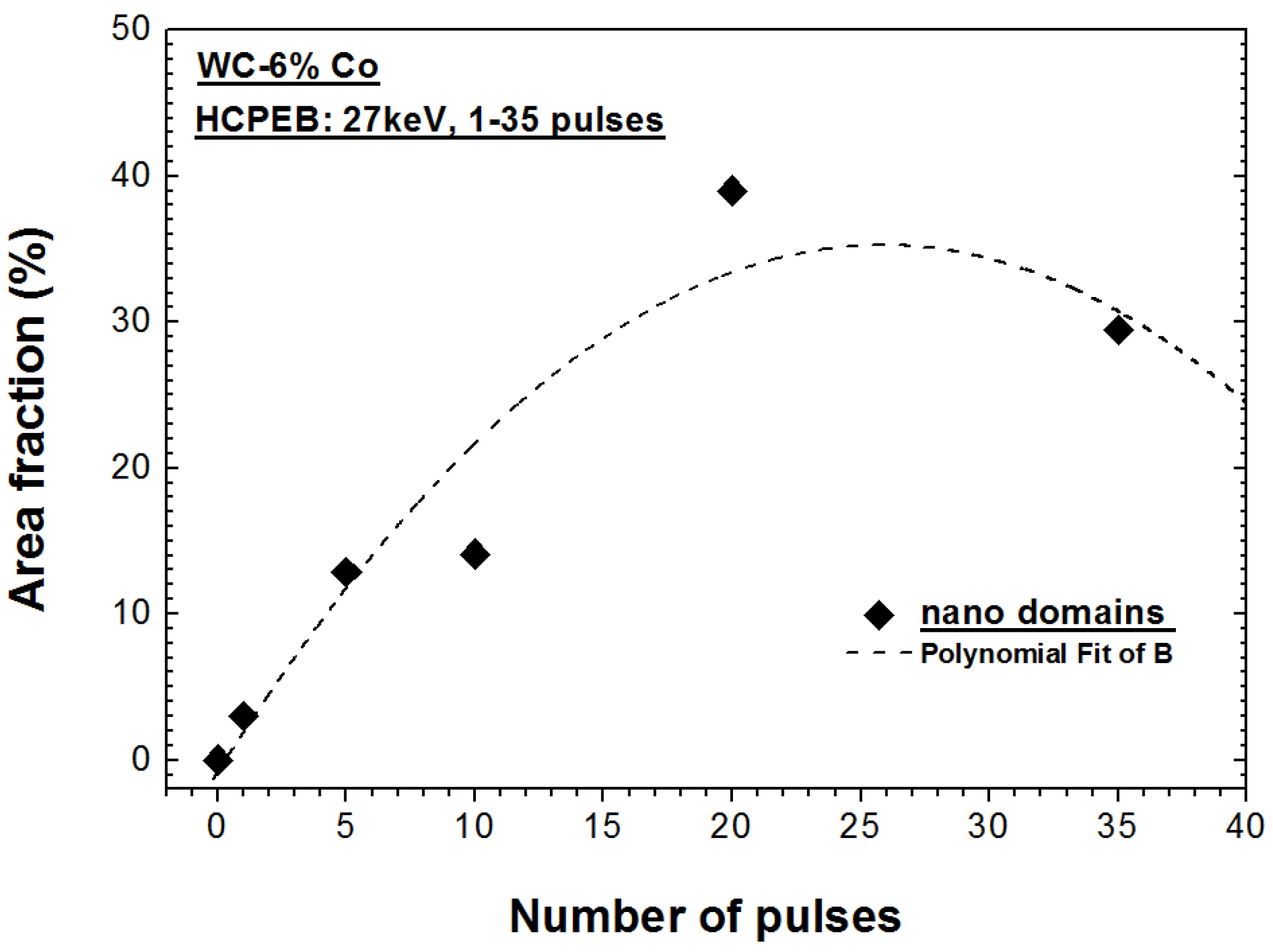
  • With the increasing number of pulses, the area fraction of the nano domains increased and reached its highest value (~40%) after 20 pulses of irradiation. After that, the area fraction of nano domains decreased slightly as a result of surface crack propagating.

Acknowledgments

This work was supported by the Natural Science Foundation (Grant Nos. 51104027, 51101026, 51401129, 51471043), the General Project of Liaoning Provincial Department of Education (L2014052) and the China Postdoctoral Science Foundation (2015M571327). The authors are grateful to Aiqun. Xu from Southeast University (China) for TEM observations.

Author Contributions

Yue Zhang, Fuyang Yu, Fuyu Dong, Yang Xu and Wubin Geng conceived, designed and performed the experiments; Yue Zhang, Fuyang Yu and Nannan Zhang analyzed the data; Nathalie Gey contributed the EBSD analysis of WC1−x phase and ternary carbides formations; Yue Zhang wrote the paper; Shengzhi Hao, Thierry Grosdidier and Chuang Dong polished the paper.

Conflicts of Interest

The authors declare no conflict of interest. The founding sponsors had no role in the design of the study; in the collection, analyses, or interpretation of data; in the writing of the manuscript, and in the decision to publish the results.

References

  1. Poate, J.M.; Foti, G.; Jacobson, D.S. Surface Modification and Alloying by Laser, Ion, and Electron Beams; Plenum Press: New York, NY, USA, 1983. [Google Scholar]
  2. Rej, D.J.; Davis, H.A.; Nastasi, M.; Olson, J.C.; Peterson, E.J.; Reiswig, R.D.; Walter, K.C.; Stinnett, R.W.; Remnev, G.E.; Struts, V.K. Surface modification of AISI-4620 steel with intense pulsed ion beams. Nucl. Instrum. Methods Phys. Res. Sect. B 1997, 127–128, 987–991. [Google Scholar] [CrossRef]
  3. Proskurovsky, D.I.; Rotshtein, V.P.; Ozur, G.E.; Markov, A.B.; Nazarov, D.S.; Shulov, V.A.; Ivanov, Y.F.; Buchheit, R.G. Pulsed electron-beam technology for surface modification of metallic materials. J. Vac. Sci. Technol. A 1998, 16, 2480–2488. [Google Scholar] [CrossRef]
  4. Wood, B.P.; Perry, A.J.; Bitteker, L.J.; Waganaar, W.J. Cratering behavior in single- and poly-crystalline copper irradiated by an intense pulsed ion beam. Surf. Coat. Technol. 1998, 108–109, 171–176. [Google Scholar] [CrossRef]
  5. Chen, X.; Yan, L.; Karnati, S.; Zhang, Y.; Liou, F. Fabrication and characterization of AlxCoFeNiCu1−x high entropy alloys by laser metal deposition. Coatings 2017, 7, 47. [Google Scholar] [CrossRef]
  6. Zhang, X.D.; Zou, J.X.; Weber, S.; Hao, S.Z.; Dong, C.; Grosdidier, T. Microstructure and property modifications in a near α Ti alloy induced by pulsed electron beam surface treatment. Surf. Coat. Technol. 2011, 206, 295–304. [Google Scholar] [CrossRef]
  7. Zhang, K.M.; Ma, J.X.; Zou, J.X.; Liu, Y.R. Surface microstructure and property modifications in a duplex stainless steel induced by high current pulsed electron beam treatments. J. Alloy. Compd. 2017, 707, 178–183. [Google Scholar] [CrossRef]
  8. Wang, H.; Hao, S.Z. Surface nanostructure and improved microhardness of 40CrNiMo7 steel induced by high current pulsed electron beam treatment. Nucl. Instrum Methods Phys Res. Sect. B 2017, 403, 45–50. [Google Scholar] [CrossRef]
  9. Hao, S.Z.; Wang, H.H.; Zhao, L.M. Surface modification of 40CrNiMo7 steel with high current pulsed electron beam treatment. Nucl. Instrum. Methods Phys. Res. Sect. B 2016, 368, 81–85. [Google Scholar] [CrossRef]
  10. Hao, S.Z.; Li, M.C. Producing nano-grained and Al-enriched surface microstructure on AZ91 magnesium alloy by high current pulsed electron beam treatment. Nucl. Instrum. Methods Phys. Res. Sect. B 2016, 375, 1–4. [Google Scholar] [CrossRef]
  11. Mateos, J.; Cuetos, J.M.; Fernandez, E.; Vijande, R. Tribological behaviour of plasma-sprayed WC coatings with and without laser remelting. Wear 2000, 239, 274–281. [Google Scholar] [CrossRef]
  12. Ivanov, Y.F.; Rotshtein, V.P.; Proskurovsky, D.I.; Orlov, P.V.; Polestchenko, K.N.; Ozur, G.E.; Goncharenko, I.M. Pulsed electron-beam treatment of WC–TiC–Co hard-alloy cutting tools: Wear resistance and microstructural evolution. Surf. Coat. Technol. 2000, 125, 251–256. [Google Scholar] [CrossRef]
  13. Ramkumar, J.; Aravindan, S.; Malhotra, S.K.; Krishnamurthy, R. Enhancing the metallurgical properties of WC insert (K-20) cutting tool through microwave treatment. Mater. Lett. 2002, 53, 200–204. [Google Scholar] [CrossRef]
  14. Gnyusov, S.; Tarasov, S.; Ivanov, Y.; Rothstein, V. The effect of pulsed electron beam melting on microstructure, friction and wear of WC–Hadfield steel hard metal. Wear 2004, 257, 97–103. [Google Scholar] [CrossRef]
  15. Ulgov, V.V.; Anishchik, V.M.; Astashinski, V.M.; Cherenda, N.N.; Gimro, L.G.; Kovyaza, A.V. Modification of WC hard alloy by compressive plasma flow. Surf. Coat. Technol. 2005, 200, 245–249. [Google Scholar] [CrossRef]
  16. Ulgov, V.V.; Kuleschov, A.K.; Soldatenko, E.A.; Koval, N.N.; Ivanov, Y.F.; Teresov, A.D. Structure, phase composition and mechanical properties of hard alloy treated by intense pulsed electron beams. Surf. Coat. Technol. 2012, 206, 2972–2976. [Google Scholar] [CrossRef]
  17. Xu, Y.; Zhang, Y.; Hao, S.Z.; Perroud, O.; Li, M.C.; Wang, H.H.; Grosdidier, T.; Dong, C. Surface microstructure and mechanical property of WC-6% Co hard alloy irradiated by high current pulsed electron beam. Appl. Surf. Sci. 2013, 279, 137–141. [Google Scholar] [CrossRef]
  18. Hao, S.Z.; Zhang, Y.; Xu, Y.; Gey, N.; Grosdidier, T.; Dong, C. Fabrication of nano graphite precipitates and WC/Co composite surface structure by using high current pulsed electron beam. Appl. Surf. Sci. 2013, 285, 552–556. [Google Scholar] [CrossRef]
  19. Hao, S.Z.; Wu, P.; Zou, J.X.; Grosdidier, T.; Dong, C. Microstructure evolution occurring in the modified surface of 316L stainless steel under high current pulsed electron beam treatment. Appl. Surf. Sci. 2007, 253, 5349–5354. [Google Scholar] [CrossRef]
  20. Zou, J.X.; Grosdidier, T.; Zhang, K.M.; Dong, C. Cross-sectional analysis of the graded microstructure in an AISI D2-steel treated with low energy high-current pulsed electron beam. Appl. Surf. Sci. 2009, 255, 4758–4764. [Google Scholar] [CrossRef]
  21. Hao, S.Z.; Yao, S.; Guan, J.; Wu, A.; Zhong, P.; Dong, C. Surface treatment of aluminum by high current pulsed electron beam. Curr. Appl. Phys. 2001, 1, 203–208. [Google Scholar] [CrossRef]
  22. Hao, S.Z.; Zhao, L.; He, D. Surface microstructure and high temperature corrosion resistance of arc-sprayed FeCrAl coating irradiated by high current pulsed electron beam. Nucl. Instrum. Methods Phys. Res. Sect. B 2013, 312, 97–103. [Google Scholar] [CrossRef]
  23. Trent, E.M.; Wright, P.K. Chapter 7-Cutting tool materials II: Cemented carbides. In Metal Cutting, 4th ed.; Elsevier: Amsterdam, The Netherlands, 2000; pp. 175–226. [Google Scholar]
  24. Zou, J.X.; Grosdidier, T.; Zhang, K.; Dong, C. Mechanisms of nanostructure and metastable phase formations in the surface melted layers of a HCPEB-treated D2 steel. Acta Mater. 2006, 54, 5409–5419. [Google Scholar] [CrossRef]
  25. Guillermet, A.F. Thermodynamic properties of the Co-W-C system. Metall. Trans. A 1989, 20, 935–956. [Google Scholar] [CrossRef]
  26. Cho, T.Y.; Yoon, J.H.; Kim, K.S.; Song, K.O.; Joo, Y.K.; Fang, W.; Zhang, S.H.; Youn, S.J.; Chun, H.G.; Hwang, S.Y. A study on HVOF coatings of micron and nano WC–Co powders. Surf. Coat. Technol. 2008, 202, 5556–5559. [Google Scholar] [CrossRef]
  27. Jafari, M.; Han, J.C.; Seol, J.B.; Park, C.G. Tribological properties of HVOF-sprayed WC-Co coatings deposited from Ni-plated powders at elevated temperature. Surf. Coat. Technol. 2017, 327, 48–58. [Google Scholar] [CrossRef]
  28. Wen, Q.F.; Liu, Y.; Wang, Y.M.; Zhang, F.G.; Zhu, X.P.; Lei, M.K. The effect of irradiation parameters of high-intensity pulsed ion beam on tribology performance of YWN8 cemented carbides. Surf. Coat. Technol. 2012, 209, 143–150. [Google Scholar] [CrossRef]
  29. Qin, Y.; Zou, J.X.; Dong, C.; Wang, X.G.; Wu, A.M.; Liu, Y.; Hao, S.Z.; Guan, Q. Temperature–stress fields and related phenomena induced by a high current pulsed electron beam. Nucl. Instrum. Methods Phys. Res. Sect. B 2004, 225, 544–554. [Google Scholar] [CrossRef]
  30. Qin, Y.; Dong, C.; Song, Z.; Hao, S.Z.; Me, X.; Li, J.; Wang, X.; Zou, J.X.; Grosdidier, T. Deep modification of materials by thermal stress wave generated by irradiation of high-current pulsed electron beams. J. Vac. Sci. Technol. A 2009, 27, 430–435. [Google Scholar] [CrossRef]
  31. Bäuerle, D. Laser Processing and Chemistry, 2nd ed.; Springer: Berlin/Heidelberg, Germany, 1996. [Google Scholar]
  32. Demetriou, M.D.; Ghoniem, N.M.; Lavine, A.S. Modeling of graphitization kinetics during peritectic melting of tungsten carbide. Acta Mater. 2002, 50, 4995–5004. [Google Scholar] [CrossRef]
Figure 1. Typical morphologies of the untreated WC-6% Co observed under electron backscattered diffraction (EBSD) with (a) phase map; (b) orientation image mapping; and (c) under TEM. The scanning step was set at 30 nm.
Coatings 07 00178 g001
Figure 2. (a) XRD patterns of WC-6% Co hard alloy and (b) the detailed XRD traces before and after high-current pulsed electron beam (HCPEB) irradiation.
Coatings 07 00178 g002
Figure 3. Phase maps on the surface of WC-6% Co hard alloy (a) before and (b) after HCPEB treatments with 1 pulse; (c) 5 pulses; (d) 10 pulses; (e) 20 pulses; and (f) 35 pulses. The scanning step was set at 30 nm.
Coatings 07 00178 g003
Figure 4. EBSD analysis on the surface of a 20-pulsed WC-Co sample: (a) SEI (Secondary electron imaging mode) micrograph; (b) corresponding EBSD orientation map; and (c) EBSD orientation taken from the selected area. The scanning step was set at 30 nm.
Coatings 07 00178 g004aCoatings 07 00178 g004b
Figure 5. TEM observations of the nano domains (a) in Co-rich binder and (b) in WC-rich area; (c) the corresponding EDAX analysis in grain A; and (d) the corresponding EDAX analysis in graphite domains.
Coatings 07 00178 g005
Figure 6. Area fraction evolution of nano domains on the surface of WC-6% Co hard alloy as-treated by HCPEB with increasing pulse numbers.
Coatings 07 00178 g006
Figure 7. (a) Surface and (b) cross-sectional aspects of WC-6% Co samples after 35 pulses of HCPEB irradiation.
Coatings 07 00178 g007
Figure 8. (a) Variation of the temperature and (b) the temperature gradient at different depth layers from the surface as a function of time.
Coatings 07 00178 g008
Figure 9. SEM morphology of a 20-pulse-HCPEB treated sample, where the black arrows indicate the dendrites growing from the WC-rich areas while the white ones indicate the formations of graphite.
Coatings 07 00178 g009

