
Ta–Zr–N Thin Films Fabricated through HIPIMS/RFMS Co-Sputtering

1
Department of Materials Engineering, Ming Chi University of Technology, New Taipei City 24301, Taiwan
2
Center for Thin Film Technologies and Applications, Ming Chi University of Technology, New Taipei City 24301, Taiwan
*
Author to whom correspondence should be addressed.
Coatings 2017, 7(11), 189; https://doi.org/10.3390/coatings7110189
Submission received: 31 August 2017
/
Revised: 19 October 2017
/
Accepted: 2 November 2017
/
Published: 4 November 2017
(This article belongs to the Special Issue Thin Film Deposition and Characterization Techniques)
Abstract
:Ta–Zr–N thin films were fabricated through co-deposition of radio-frequency magnetron sputtering and high-power impulse magnetron sputtering (HIPIMS/RFMS co-sputtering). The oxidation resistance of the fabricated films was evaluated by annealing the samples in a 15-ppm O2-N2 atmosphere at 600 °C for 4 and 8 h. The mechanical properties and surface roughness of the as-deposited and annealed thin films were evaluated. The results indicated that the HIPIMS/RFMS co-sputtered Ta–Zr–N thin films exhibited superior mechanical properties and lower surface roughness than did the conventional direct current-sputtered Ta–Zr–N thin films and HIPIMS-fabricated ZrNx thin films in both the as-deposited and annealed states.
1. Introduction
Ta–Zr–N coatings have been employed as protective coatings against wear for biomedical implants [1,2] and as diffusion barrier layers in Cu metallization [3]. Ta-rich Ta–Zr–N coatings exhibited enhanced toughness with high hardness [4,5]. In a previous study [6], low-Zr-content Ta1−xZrxNy thin films (x = 0–0.17, y = 0.86–1.03) fabricated through conventional reactive direct-current (DC) magnetron co-sputtering exhibited desirable mechanical properties and a restricted increase in surface roughness from 0.9–1.5 nm to 1.2–1.7 nm after annealing at 600 °C in a 15-ppm O2-N2 atmosphere for 4 h. The chemical inertness of these films against commercial moldable SiO2–B2O3–BaO-based glass after 500 thermal cycles was experimentally confirmed. Thermal cycling annealing at 270 °C and 600 °C in a 15-ppm O2-N2 atmosphere was a realistic mass production process [7,8]. The smoothing mechanism of coating surfaces is a crucial factor when Ta–Zr–N thin films are deposited as the protective coatings on glass molding dies. High-power pulsed magnetron sputtering (also called high-power impulse magnetron sputtering (HIPIMS) [9,10]) has broadened the operating window of magnetron sputtering. HIPIMS was proposed as a method for growing high-quality films with dense structure, smooth morphology, and excellent adhesion [11], and has attracted substantial industry and research interest because of its potential use in such applications as wear resistance [11,12] and electric coatings [13]. However, despite its superiority, the mechanism underlying HIPIMS is complex because many factors—particularly pulse parameters—affect the deposition process. The low deposition rate in the HIPIMS process became a drawback for the commercial applications [10,14]. Therefore, hybrid processes, such as HIPIMS/DCMS (direct-current magnetron co-sputtering) [15] and HIPIMS/AIP (arc ion plating) [16] were utilized. In this study, co-deposition of radio-frequency magnetron sputtering and HIPIMS (hereafter, HIPIMS/RFMS co-sputtering) was used to improve the surface quality (decrease the surface roughness) of Ta–Zr–N thin films, and its effects on the mechanical properties and oxidation resistance of the films were investigated.
2. Materials and Methods
An HIPIMS/RFMS co-sputtering system (Figure 1) was employed to deposit Ta–Zr–N thin films on silicon substrates. A 99.95% pure Ta target was connected to an RF power generator (13.56 MHz), and a 99.9% pure Zr target was connected to a SPIK2000A pulse power supply (SPIK 2000A; Shen Chang Electric Co., Taipei, Taiwan) operated in the unipolar negative mode at a constant power of 400 W. Both targets were 76.2 mm in diameter, and tilted to the vertical axis. The pulse on-time, ton, and pulse off-time, toff, were kept constant at 100 and 3900 µs, respectively. The duty cycle (ton/(toff + ton) × 100%) was maintained at 2.5%. The substrate-to-target vertical distance was 12 cm, and the chamber was pumped to a base pressure of 6.7 × 10⁻⁴ Pa. The working pressure was maintained at approximately 0.67 Pa by flowing an Ar and N2 (Ar:N2 = 9:1) gas mixture into the chamber. The substrate holder was rotated at 10 rpm during the process. A pulse bias voltage of −50 V was applied to the substrate holder, and the coatings were deposited at 400 °C. Table 1 lists the sputtering powers employed to fabricate the Ta–Zr–N thin films; the deposition times were altered to achieve coating thicknesses of 1217–1279 nm. The Ta–Zr–N thin films were further annealed at 600 °C for 4 and 8 h in a 15-ppm O2-N2 atmosphere in a quartz tube furnace.
Chemical composition analysis was conducted by using a field-emission electron probe microanalyzer (FE-EPMA, JXA-8500F, JEOL, Akishima, Japan) on the surface of the samples. The film and oxide scale thicknesses were evaluated by field emission scanning electron microscopy (FE-SEM, S4800, Hitachi, Tokyo, Japan) on the fracture surface of the samples, initiated from the backside of Si wafers. A conventional X-ray diffractometer (XRD, X’Pert PRO MPD, PANalytical, Almelo, The Netherlands) with Cu Kα radiation was adopted to identify the phases of the coatings, using the grazing incidence technique with an incidence angle of 1°. The nanostructure of the coatings and scales was further examined using transmission electron microscopy (TEM, JEM-2010F, JEOL, Akishima, Japan) at a 200-kV accelerating voltage. TEM samples were prepared by applying a focused ion beam system (FEI Nova 200, Hillsboro, OR, USA) at an accelerating voltage of 30 kV with a gallium ion source. A Pt layer was deposited to protect the free surface during sample preparation. The surface nanoindentation hardness values of Ta1−xZrxNy coatings were measured with a nanoindentation tester (TI-900 Triboindenter, Hysitron, Eden Prairie, MN, USA). The nanoindenter was equipped with a Berkovich diamond probe tip. The applied load was controlled to exhibit an indentation depth of 100 nm. The loading, holding, and unloading times were 5 s each. The nanoindentation hardness and reduced elastic modulus Er of each indent were calculated based on the Oliver and Pharr method [17]. The elastic modulus, E, of a film can be determined from:
where E, ν, Ei, and νi are the elastic modulus and Poisson’s ratio of the film and indenter, using ν = 0.25, Ei = 1141 GPa, and νi = 0.07 [18], respectively. The surface roughness values of the coatings were evaluated by using an atomic force microscope (AFM, Dimension 3100 SPM, NanoScope IIIa, Veeco, New York, NY, USA). The scanning area of each image was set at 5 μm × 5 μm with a scanning rate of 1.0 Hz. The residual stress of the films measured by the curvature method was calculated using Stoney’s equation [19].
3. Results and Discussion
3.1. As-Deposited Ta–Zr–N Thin Films
Table 2 lists the elemental compositions of the as-deposited Ta–Zr–N thin films prepared through HIPIMS/RFMS co-sputtering. The Ta content in the Ta–Zr–N thin films increased with increasing Ta target power. The oxygen content in the as-deposited states were 1.0–2.3 at %. The samples were designated in the form Ta1−xZrxNy, as follows: Ta0.84Zr0.16N0.40, Ta0.81Zr0.19N0.52, Ta0.58Zr0.42N0.59, and Ta0.33Zr0.67N0.68. The atomic ratio of N/(Ta + Zr) increased from 0.40 to 0.52, 0.59, and 0.68 as the power of the Ta target increased from 100 to 200, 300, and 400 W, respectively. The deposition parameters were adjusted to fabricate thin films of similar thicknesses (Table 1); the Ta0.84Zr0.16N0.40, Ta0.81Zr0.19N0.52, Ta0.58Zr0.42N0.59, and Ta0.33Zr0.67N0.68 thin films were 1253, 1279, 1238, and 1217 nm thick, respectively.
Figure 2 shows the grazing-incident XRD patterns of the as-deposited Ta–Zr–N thin films. Although the atomic ratio of N/(Ta + Zr) deviated from the stoichiometric value of 1, the Ta0.81Zr0.19N0.52, Ta0.58Zr0.42N0.59, and Ta0.33Zr0.67N0.68 thin films exhibited a face-centered cubic (fcc) structure. For transition-metal-nitride coatings, N vacancy concentrations can be up to 50% [20]. Matenoglou et al. [21] reported that the ternary transition metal nitrides TaxMe1−xN (Me = Ti, Zr, Hf, Nb, Ta, Mo, W) formed solid solutions over the entire x range (0 < x < 1) and that they were stable in the rock-salt structure regardless of the valence electron configuration of its constituent metals. Furthermore, the reflections shift left as Zr content in the Ta–Zr–N thin films increases because the lattice parameters of standard cubic TaN and ZrN are 0.4340 nm (ICDD 49-1283) and 0.4577 nm (ICDD 35-0753), respectively. By contrast, the Ta0.84Zr0.16N0.40 thin film exhibited a mixture of hexagonal β-Ta[89-1545], hexagonal γ-Ta2N (ICDD 26-0985), and cubic ZrN phases, which is attributable to the severe lack of N content in the thin films. Since the standard Gibbs free energies of the metal nitride formation of TaN, Ta2N, and ZrN at 400 °C are −391,001 J/(mol of N2), −420,567 J/(mol of N2), and −602,902 J/(mol of N2) [22], respectively, ZrN formed preferentially, followed by Ta2N. The deficiency of N in the Ta0.84Zr0.16N0.40 coating resulted in that an excess Ta remained in the β-Ta phase but no N atoms were available to form TaN. The N content of the Ta–Zr–N thin films decreased with increasing power supplied on the Ta target (WTa), which was attributed to the re-sputtering of N atoms from the surface resulting from the increasing energy of bombarding ions [23,24].
Figure 3 and Figure 4 present the AFM and cross-sectional SEM images of the as-deposited Ta–Zr–N thin films, respectively. The Ta0.84Zr0.16N0.40, Ta0.81Zr0.19N0.52, and Ta0.58Zr0.42N0.59 thin films exhibited a smooth surface and a dense structure with a surface roughness of 0.4–0.5 nm (Table 3). By contrast, the Ta0.33Zr0.67N0.68 thin film exhibited a coarser columnar structure with a high surface roughness of 2.5 nm. The film structure transition from columnar to dense non-columnar was attributed to the increasing energy of bombarding ions [25,26].
Table 3 shows the mechanical properties of the as-deposited Ta–Zr–N thin films prepared on Si substrates. The nanoindentation hardness of fcc Ta0.81Zr0.19N0.52, Ta0.58Zr0.42N0.59, and Ta0.33Zr0.67N0.68 thin films were 35.5, 35.0, and 30.2 GPa, respectively, whereas the nanoindentation hardness of the Ta0.84Zr0.16N0.40 thin film with mixed phases was 31.9 GPa. The elastic moduli of Ta0.81Zr0.19N0.52, Ta0.58Zr0.42N0.59, and Ta0.33Zr0.67N0.68 thin films were similar (299, 311, and 306 GPa, respectively) because elastic modulus is an intrinsic material property dependent on atomic bonding and crystalline structure [27]. By contrast, the elastic modulus of the Ta0.84Zr0.16N0.40 thin film exhibited a lower value of 258 GPa, which was attributed to the implantation of a soft Ta phase. The H3/E2 values indicate a resistance to plastic deformation [28], and were 0.49, 0.50, 0.44, and 0.30 for the Ta0.84Zr0.16N0.40, Ta0.81Zr0.19N0.52, Ta0.58Zr0.42N0.59, and Ta0.33Zr0.67N0.68 thin films, respectively. The elastic recovery We [29] of the as-deposited Ta–Zr–N thin films exhibited a level of 67%–76%. In a previous study using the same sputtering system [30], the HIPIMS-fabricated ZrNx thin films (x = 0.65–0.78) exhibited a hardness of 26–27 GPa, a Young’s modulus of 260–290 GPa, a residual stress of −4.2–−5.2 GPa, and a surface roughness of approximately 0.5 nm in the as-deposited state. The introduction of Ta into the ZrN-based thin films evidently raised the hardness values and maintained similar Young’s modulus levels.
Aouadi [2] reported the mechanical properties of overstoichiometric Ta–Zr–N films deposited by reactive unbalanced magnetron DC sputtering, which exhibited a hardness of <30 GPa with a wide range of Ta/(Ta + Zr) ratios (0.16–0.78) except for the film with a Ta/(Ta + Zr) ratio of 0.29, which exhibited a sudden increased hardness of 37 GPa attributed to solid solution hardening and limited segregation of solutes at grain boundaries. Abadias et al. [4,5] reported a hardness level of ~30 GPa for Zr1−xTaxN films (x = 0.51–0.78) prepared using DC magnetron co-sputtering. The residual stress was −4.65, −4.84, −6.17, and −4.18 GPa for the as-deposited Ta0.84Zr0.16N0.40, Ta0.81Zr0.19N0.52, Ta0.58Zr0.42N0.59, and Ta0.33Zr0.67N0.68 thin films (Table 3), respectively. These values were more negative than those with similar Zr/(Ta + Zr) ratios reported in our previous study [6], in which the residual stress of the DC-sputtered Ta1−xZrxNy thin films (x = 0.17–0.72, y = 1.03–1.09) ranged from 0 to −2.11 GPa. Residual stress affects the hardness of the coatings; in other words, compressive stress increases coating hardness, whereas tensile stress reduces it [31]. The as-deposited Ta–Zr–N thin films with a wide Zr/(Ta + Zr) ratio range of 0.16–0.67 fabricated in this study exhibited nanoindentation hardnesses of 30–35 GPa, superior to the 22–26 GPa reported for the DC-sputtered Ta0.83Zr0.17N1.03, Ta0.59Zr0.41N1.09, and Ta0.28Zr0.72N1.05 thin films [6].
3.2. Ta–Zr–N Thin Films Annealed in a 15-ppm O2-N2 Atmosphere at 600 °C
Table 2 lists the elemental compositions of the Ta–Zr–N thin films annealed at 600 °C in a 15-ppm O2–N2 atmosphere for 4 and 8 h. The atomic ratios of Zr/(Ta + Zr) of the annealed Ta0.58Zr0.42N0.59 and Ta0.33Zr0.67N0.68 thin films retained their values in the as-deposited states (0.42 and 0.67, respectively), whereas the Zr/(Ta + Zr) ratios of the annealed Ta0.84Zr0.16N0.40 and Ta0.81Zr0.19N0.52 thin films increased from 0.16 to 0.23 and from 0.19 to 0.31, respectively. By contrast, the atomic ratios of Ta:Zr of the DC-sputtered Ta1−xZrxNy thin films (x = 0.05–0.72, y = 0.97–1.05) [6] retained their preannealing values after annealing at 600 °C in 15-ppm O2-N2 for 4 h. Moreover, the DC-sputtered Ta1−xZrxNy thin films were near-stoichiometric, whereas the Ta–Zr–N thin films in this study were understoichiometric. Furthermore, the DC-sputtered Ta1−xZrxNy thin films with a higher Zr content gathered a higher O content after annealing, which was in contrast to the Ta–Zr–N thin films prepared in this study. The HIPIMS/RFMS-fabricated Ta–Zr–N thin films with a lower Zr content gathered a higher O content after annealing. These results implied that the variations of Zr/(Ta + Zr) ratio and O content of the annealed Ta–Zr–N thin films in this study were caused by nonstoichiometric compositions, which contributed a high degree of nonmetal site vacancies in the nitride structure; therefore, O quickly diffused inward. Conversely, Zr preferentially diffused outward and reacted with O to form ZrO2 around the near-surface region because Zr possesses a lower mass than Ta does, and because the standard Gibbs free energies of the metal oxide formations of ZrO2 and Ta2O5 at 600 °C are −931,249 and −663,572 J per mole of oxygen molecules [22], respectively. Since ZrO2 was the dominant oxide and is not volatile, and the chemical composition analysis was conducted on the surface, the Zr/(Ta + Zr) ratios maintained and increased for the high- and low-Zr-content films, respectively. The N/(Ta + Zr) ratios of the annealed Ta0.81Zr0.19N0.52, Ta0.58Zr0.42N0.59, and Ta0.33Zr0.67N0.68 thin films decreased slightly due to the replacement of N by O in the beginning of oxidation, whereas the N/(Ta + Zr) ratio of the annealed Ta0.84Zr0.16N0.40 thin films maintained a level similar to that at the as-deposited state due to the high degree of understoichiometric structure.
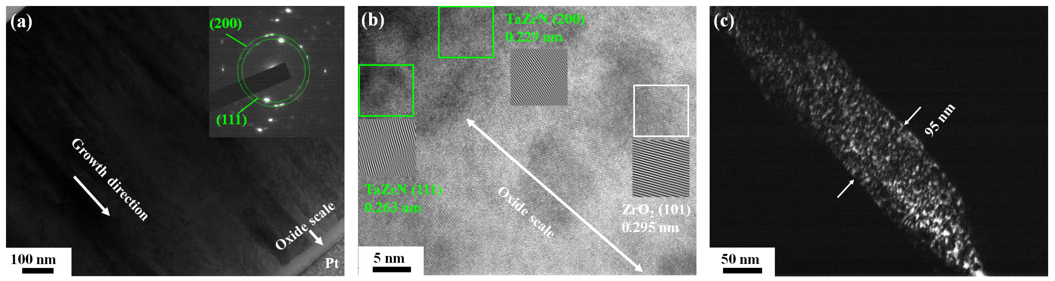
The XRD patterns of the 4-h-annealed Ta–Zr–N thin films (data not shown) did not differ from those of the corresponding as-deposited thin films. Figure 5 presents the XRD patterns of the 8-h-annealed Ta–Zr–N thin films, which also exhibited reflections similar to those of the as-deposited thin films except that a wide diffraction reflection appeared at the 2θ angle of approximately 30° for the Ta0.33Zr0.67N0.68 thin film, which is attributable to the formation of a surface oxide scale comprising ZrO2. The thicknesses of surface oxide scales were 131, 136, 62, and 0 nm and 221, 195, 151, and 41 nm (Figure 6) for the 4- and 8-h-annealed Ta0.84Zr0.16N0.40, Ta0.81Zr0.19N0.52, Ta0.58Zr0.42N0.59, and Ta0.33Zr0.67N0.68 thin films, respectively. Figure 7a shows the cross-sectional TEM image of the 8-h-annealed Ta0.58Zr0.42N0.59 thin film, whose selected area diffraction pattern exhibits an fcc phase. The high-resolution image (Figure 7b) of the outermost surface region exhibits an amorphous oxide scale of approximately 13 nm. Lattice fringes with d-spacings of 0.224 and 0.259 nm, which respectively correlate to the stacking of (200) and (111) planes, were identified beneath the outermost surface oxide region. The dark-field image corresponding to the (111) diffraction spot in Figure 7a reveals a fine columnar structure with a width of 30 nm (Figure 7c). Figure 8a shows the cross-sectional TEM image of the 8-h-annealed Ta0.33Zr0.67N0.68 thin film, whose columnar structure and diffraction pattern are more evident than those of the annealed Ta0.58Zr0.42N0.59 thin film. Figure 8b indicates that crystalline ZrO2 domains were observed in the surface oxide scale of the annealed Ta0.33Zr0.67N0.68 thin film. The lattice fringes of (200) and (111) planes in the columnar nitride structure show d-spacings of 0.229 and 0.263 nm, respectively. Figure 8c exhibits the dark-field image corresponding to the (111) diffraction spot in Figure 8a and reveals a coarser columnar width of 95 nm. The oxide scales of Ta0.84Zr0.16N0.40 and Ta0.81Zr0.19N0.52 were inferred to be amorphous because no oxide reflections were observed in their XRD patterns.
The vital characteristics of the protective coatings on glass molding dies were high hardness, low surface roughness, and chemical inertness against moldable optical glasses [6,8,32,33]. The formation of amorphous surface oxide scales on high-Ta-content Ta–Zr–N thin films restricted the increase in surface roughness relative to that of crystalline oxide scales formed on high-Zr-content Ta0.33Zr0.67N0.68 thin films (Table 3). Since the hardness values of the moldable optical glasses ranged from 3.2 to 7.0 GPa, the protective coatings with a hardness higher than 10 GPa were preferred [8]. Although the hardness measurement of the annealed thin films included the contribution of surface oxide scale, this hardness value implied a realistic strength against the glasses in the molding process. The nanoindentation hardnesses decreased to 20.9, 21.5, 25.7, and 28.3 GPa for the 4-h-annealed Ta0.84Zr0.16N0.40, Ta0.81Zr0.19N0.52, Ta0.58Zr0.42N0.59, and Ta0.33Zr0.67N0.68 thin films (Table 3), respectively; furthermore, the nanoindentation hardnesses decreased to 18.0, 19.5, 24.8, and 19.3 GPa after 8 h of annealing, respectively. Both the H3/E2 ratio and elastic recovery We exhibited decreased trends with increasing the annealing time due to the formation of surface oxide. The residual stress of annealed Ta0.84Zr0.16N0.40 and Ta0.81Zr0.19N0.52 thin films decreased to a range of −2.6 to −3.5 GPa (Table 3). The annealed Ta0.58Zr0.42N0.59 and Ta0.33Zr0.67N0.68 thin films exhibited local detachment after annealing; hence, the residual stress could not be evaluated. In a previous study [30], the nanoindentation hardness values of the HIPIMS-fabricated ZrNx thin films declined from 26–27 GPa to less than 10 GPa after they were annealed at 600 °C in 15 ppm O2–N2 for 2 h owing to the formation of crystalline ZrO2 scales, which was accompanied by an increase in the surface roughness from 0.5 to 3–6 nm.
4. Conclusions
We reported the preparation of understoichiometric Ta–Zr–N thin films with atomic ratios (N/(Ta + Zr)) of 0.40–0.68 through HIPIMS/RFMS co-sputtering. The as-deposited high-Ta-content Ta–Zr–N thin films Ta0.84Zr0.16N0.40, Ta0.81Zr0.19N0.52, and Ta0.58Zr0.42N0.59 exhibited nanoindentation hardnesses of 32–35 GPa, Young’s moduli of 258–311 GPa, H3/E2 values of 0.44–0.50 GPa, elastic recovery of 73%–76%, and surface roughnesses of 0.4–0.5 nm. The HIPIMS technique helps to fabricate dense and smooth thin films. After annealing at 600 °C in a 15-ppm O2-N2 atmosphere for 4 h, the nanoindentation hardnesses decreased to 21–26 GPa and the surface roughnesses increased to 0.5–1.1 nm. The nanoindentation hardnesses further decreased to 18–25 GPa and the surface roughnesses further increased to 1.2–1.6 nm after 8 h of annealing. The introduction of Ta into the HIPIMS-fabricated ZrN thin films evidently raised the hardness values in the as-deposited state and varied the oxide scale to be a ZrO2-dominant amorphous layer after annealing; the amorphous layer decreased the oxidation rate and reduced the declining trend of the hardness during annealing. Amorphous surface oxide scales restricted an increase in surface roughness. The HIPIMS/RFMS-co-sputtered Ta–Zr–N thin films exhibited a nanoindentation hardness of 30–35 GPa with a Zr/(Ta + Zr) ratio range of 0.16–0.67; this range was wider than those of the conventional DC-sputtered Ta–Zr–N thin films with a hardness >30 GPa.
Acknowledgments
The financial supports of this work from the Ministry of Science and Technology, Taiwan, under contract nos. 104-2622-E-131-005 and 105-2221-E-131-004 are appreciated.
Author Contributions
Li-Chun Chang designed the experiments and wrote the paper; Ching-Yen Chang performed the experiments; and Ya-Wen You analyzed the TEM data.
Conflicts of Interest
The authors declare no conflict of interest. The founding sponsors had no role in the design of the study; in the collection, analyses, or interpretation of data; in the writing of the manuscript; or in the decision to publish the results.
References
- Aouadi, S.M.; Filip, P.; Debessai, M. Characterization of tantalum zirconium nitride sputter-deposited nanocrystalline coatings. Surf. Coat. Technol. 2004, 187, 177–184. [Google Scholar] [CrossRef]
- Aouadi, S.M. Structural and mechanical properties of TaZrN films: Experimental and ab initio studies. J. Appl. Phys. 2006, 99, 053507. [Google Scholar] [CrossRef]
- Ruan, J.L.; Huang, J.L.; Lu, H.H.; Chen, J.S.; Lii, D.F. Effects of the Ta content on the microstructure and electrical property of reactively sputtered TaxZr1−xN thin films. Thin Solid Films 2011, 519, 4987–4991. [Google Scholar] [CrossRef]
- Abadias, G.; Kanoun, M.B.; Goumri-Said, S.; Koutsokeras, L.; Dub, S.N.; Djemia, P. Electronic structure and mechanical properties of ternary ZrTaN alloys studied by ab initio calculations and thin-film growth experiments. Phys. Rev. B 2014, 90, 114107. [Google Scholar] [CrossRef]
- Abadias, G.; Djemia, P.; Belliard, L. Alloying effects on the structure and elastic properties of hard coatings based on ternary transition metal (M = Ti, Zr or Ta) nitrides. Surf. Coat. Technol. 2014, 257, 129–137. [Google Scholar] [CrossRef]
- Chang, L.C.; Chang, C.Y.; Chen, Y.I. Mechanical properties and oxidation resistance of reactively sputtered Ta1−xZrxNy thin films. Surf. Coat. Technol. 2015, 280, 27–36. [Google Scholar] [CrossRef]
- Liu, S.C.; Chen, Y.I.; Tsai, H.Y.; Lin, K.C.; Chen, Y.H. Thermal stability of Ir–Re coatings annealed in oxygen-containing atmospheres. Surf. Coat. Technol. 2013, 237, 105–111. [Google Scholar] [CrossRef]
- Liu, S.C.; Chen, Y.I.; Shyu, J.J.; Tsai, H.Y.; Lin, K.Y.; Chen, Y.H.; Lin, K.C. The chemical inertness of Ir–Re and Ta–Ru coatings in molding B2O3–ZnO–La2O3-based glass. Surf. Coat. Technol. 2014, 259, 352–357. [Google Scholar] [CrossRef]
- Kouznetsov, V.; Macák, K.; Schneider, J.M.; Helmersson, U.; Petrov, I. Functional differences between the external and protoplasmic surfaces of plasma membranes in activating vaccinia virus infectivity. Surf. Coat. Technol. 1990, 122, 290–293. [Google Scholar] [CrossRef]
- Helmersson, U.; Lattemann, M.; Bohlmark, J.; Ehiasarian, A.P.; Gudmundsson, J.T. Ionized physical vapor deposition (IPVD): A review of technology and applications. Thin Solid Films 2006, 513, 1–24. [Google Scholar] [CrossRef]
- Purandare, Y.P.; Ehiasarian, A.P.; Hovsepian, P.E. Structure and properties of ZrN coatings deposited by high power impulse magnetron sputtering technology. J. Vac. Sci. Technol. A 2011, 29, 011004. [Google Scholar] [CrossRef]
- Schmidt, S.; Czigány, Z.; Greczynski, G.; Jensen, J.; Hultman, L. Influence of inert gases on the reactive high power pulsed magnetron sputtering process of carbon-nitride thin films. J. Vac. Sci. Technol. A 2013, 31, 011503. [Google Scholar] [CrossRef] [Green Version]
- Magnus, F.; Ingason, A.S.; Olafsson, S.; Gudmundsson, J.T. Nucleation and resistivity of ultrathin TiN films grown by high-power impulse magnetron sputtering. IEEE Electron. Dev. Lett. 2012, 33, 1045–1047. [Google Scholar] [CrossRef]
- Alami, J.; Sarakinos, K.; Mark, G.; Wuttig, M. On the deposition rate in a high power pulsed magnetron sputtering discharge. Appl. Phys. Lett. 2006, 89, 154104. [Google Scholar] [CrossRef]
- Greczynski, G.; Lu, J.; Jensen, J.; Bolz, S.; Kölker, W.; Schiffers, C.; Lemmer, O.; Greene, J.E.; Hultman, L. A review of metal-ion-flux-controlled growth of metastable TiAlN by HIPIMS/DCMS Co-sputtering. Surf. Coat. Technol. 2014, 257, 15–25. [Google Scholar] [CrossRef]
- Ding, J.; Zhang, T.; Yun, J.M.; Kang, M.C.; Wang, Q.; Kim, K.H. Microstructure, mechanical, oxidation and corrosion properties of the Cr-Al-Si-N coatings deposited by a hybrid sputtering system. Coatings 2017, 7, 119. [Google Scholar] [CrossRef]
- Oliver, W.C.; Pharr, G.M. An improved technique for determining hardness and elastic modulus using load and displacement sensing indentation experiments. J. Mater. Res. 1992, 7, 1564–1583. [Google Scholar] [CrossRef]
- Simmons, G.; Wang, H. Single Crystal Young’s Constants and Calculated Aggregate Properties: A Handbook; MIT Press: Cambridge, MA, USA, 1971. [Google Scholar]
- Janssen, G.C.A.M.; Abdalla, M.M.; van Keulen, F.; Pujada, B.R.; van Venrooy, B. Celebrating the 100th anniversary of the Stoney equation for film stress: Developments from polycrystalline steel strips to single crystal silicon wafers. Thin Solid Films 2009, 517, 1858–1867. [Google Scholar] [CrossRef]
- Thod, L.E. Transition Metal Carbides and Nitrides; Academic Press: New York, NY, USA, 1971. [Google Scholar]
- Matenoglou, G.M.; Koutsokeras, L.E.; Lekka, C.E.; Abadias, G.; Kosmidis, C.; Evangelakis, G.A.; Patsalas, P. Structure, stability and bonding of ternary transition metal nitrides. Surf. Coat. Technol. 2009, 204, 911–914. [Google Scholar] [CrossRef]
- Barin, I. Thermochemical Data of Pure Substances, 3rd ed.; VCH: New York, NY, USA, 1995. [Google Scholar]
- Hurkmans, T.; Lewis, D.B.; Paritong, H.; Brooks, J.S.; Münz, W.D. Influence of ion bombardment on structure and properties of unbalanced magnetron grown CrNx coatings. Surf. Coat. Technol. 1999, 114, 52–59. [Google Scholar] [CrossRef]
- Musil, J.; Šícha, J.; Heřman, D.; Čerstvý, R. Role of energy in low-temperature high-rate formation of hydrophilic TiO2 thin films using pulsed magnetron sputtering. J. Vac. Sci. Technol. A 2007, 25, 666–674. [Google Scholar] [CrossRef]
- Musil, J. Hard nanocomposite coatings: Thermal stability, oxidation resistance and toughness. Surf. Coat. Technol. 2012, 207, 50–65. [Google Scholar] [CrossRef]
- Musil, J.; Jaroš, M.; Čerstvý, R.; Haviar, S. Evolution of microstructure and macrostress in sputtered hard Ti(Al,V)N films with increasing energy delivered during their growth by bombarding ions. J. Vac. Sci. Technol. A 2017, 35, 020601. [Google Scholar] [CrossRef]
- Zhou, Y.L.; Niinomi, M.; Akahori, T. Changes in mechanical properties of Ti alloys in relation to alloying additions of Ta and Hf. Mater. Sci. Eng. A 2008, 483–484, 153–156. [Google Scholar] [CrossRef]
- Tsui, T.Y.; Pharr, G.M.; Oliver, W.C.; Bhatia, C.S.; White, R.L.; Anders, S.; Anders, A.; Brown, I.G. Nanoindentation and nanoscratching of hard carbon coatings for magnetic disks. Mater. Res. Soc. Symp. Proc. 1995, 383, 447–452. [Google Scholar] [CrossRef]
- Musil, J.; Kunc, F.; Zeman, H.; Poláková, H. Relationships between hardness, Young’s modulus and elastic recovery in hard nanocomposite coatings. Surf. Coat. Technol. 2002, 154, 304–313. [Google Scholar] [CrossRef]
- Chang, L.C.; Chang, C.Y.; Chen, Y.I.; Kao, H.L. Mechanical properties and oxidation behavior of ZrNx thin films fabricated through high-power impulse magnetron sputtering deposition. J. Vac. Sci. Technol. A 2016, 34, 02D107. [Google Scholar] [CrossRef]
- Bielawski, M. Residual stress control in TiN/Si coatings deposited by unbalanced magnetron sputtering. Surf. Coat. Technol. 2006, 200, 3987–3995. [Google Scholar] [CrossRef]
- Chen, Y.I.; Wang, H.H. Oxidation resistance and mechanical properties of Cr–Ta–Si–N coatings in glass molding processes. Surf. Coat. Technol. 2014, 260, 118–125. [Google Scholar] [CrossRef]
- Chen, Y.I.; Cheng, Y.R.; Chang, L.C.; Lu, T.S. Chemical inertness of Ta–Si–N coatings in glass molding. Thin Solid Films 2015, 584, 66–71. [Google Scholar] [CrossRef]
Figure 1.
Schematic image of the radio-frequency magnetron sputtering and high-power impulse magnetron sputtering (HIPIMS/RFMS) co-sputtering equipment.
Figure 1.
Schematic image of the radio-frequency magnetron sputtering and high-power impulse magnetron sputtering (HIPIMS/RFMS) co-sputtering equipment.
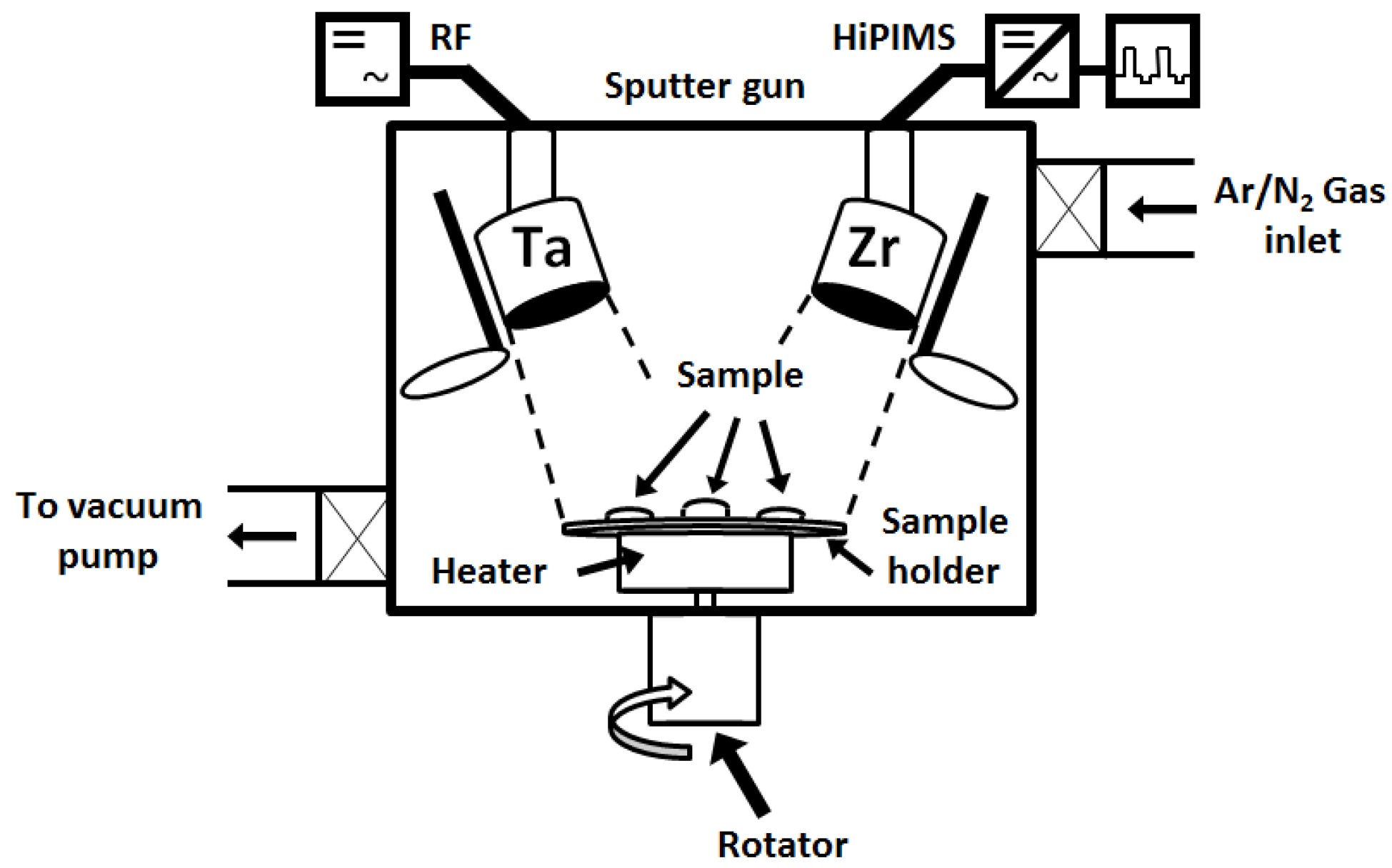
Figure 2.
XRD patterns of as-deposited Ta–Zr–N thin films prepared on Si substrates.
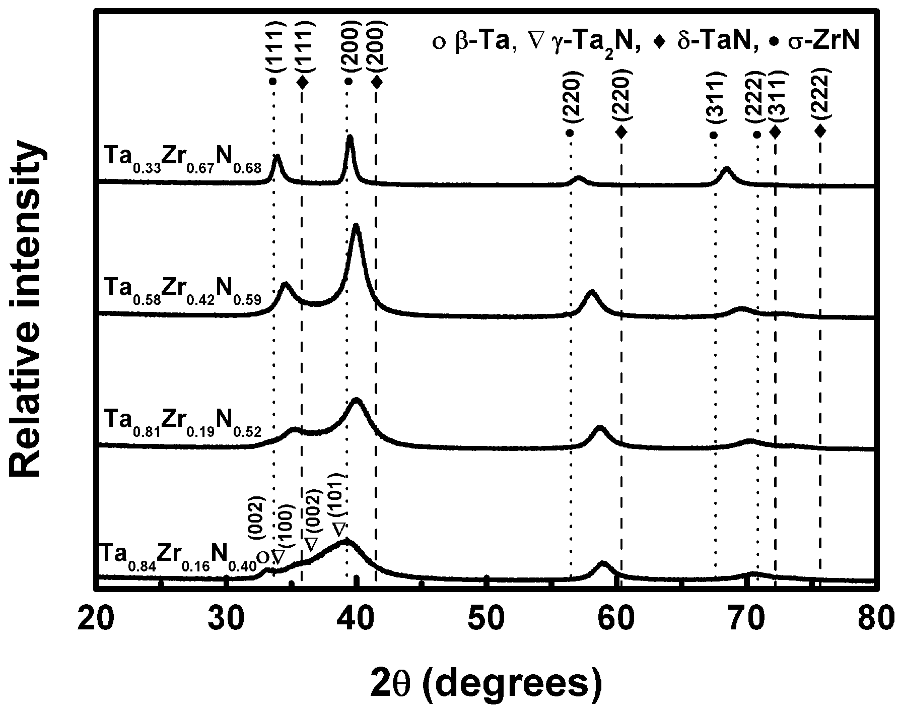
Figure 3.
Atomic force microscopy (AFM) images of as-deposited Ta–Zr–N thin films prepared on Si substrates. (a) Ta0.84Zr0.16N0.40; (b) Ta0.81Zr0.19N0.52; (c) Ta0.58Zr0.42N0.59; (d) Ta0.33Zr0.67N0.68.
Figure 3.
Atomic force microscopy (AFM) images of as-deposited Ta–Zr–N thin films prepared on Si substrates. (a) Ta0.84Zr0.16N0.40; (b) Ta0.81Zr0.19N0.52; (c) Ta0.58Zr0.42N0.59; (d) Ta0.33Zr0.67N0.68.
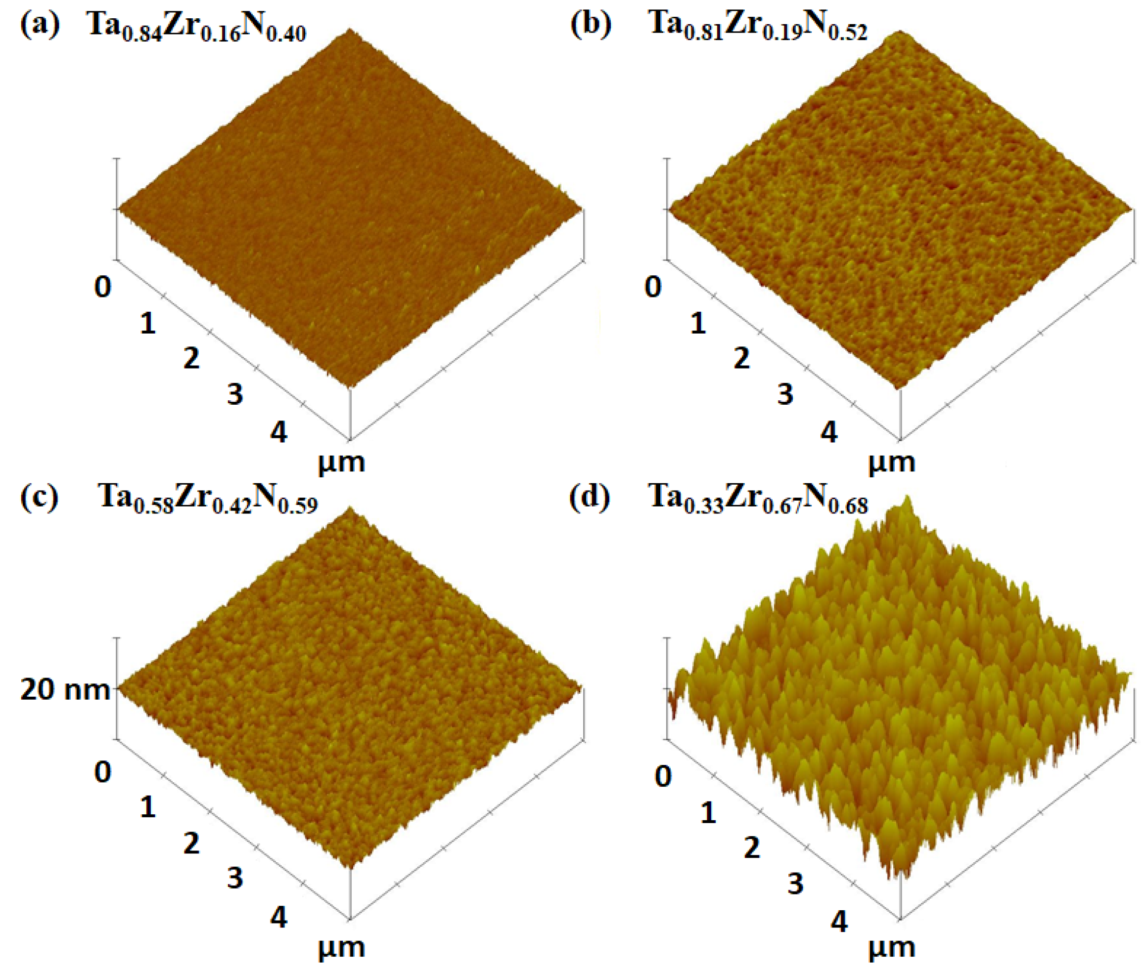
Figure 4.
Cross-sectional SEM images of as-deposited Ta–Zr–N thin films prepared on Si substrates. (a) Ta0.84Zr0.16N0.40; (b) Ta0.81Zr0.19N0.52; (c) Ta0.58Zr0.42N0.59; (d) Ta0.33Zr0.67N0.68.
Figure 4.
Cross-sectional SEM images of as-deposited Ta–Zr–N thin films prepared on Si substrates. (a) Ta0.84Zr0.16N0.40; (b) Ta0.81Zr0.19N0.52; (c) Ta0.58Zr0.42N0.59; (d) Ta0.33Zr0.67N0.68.
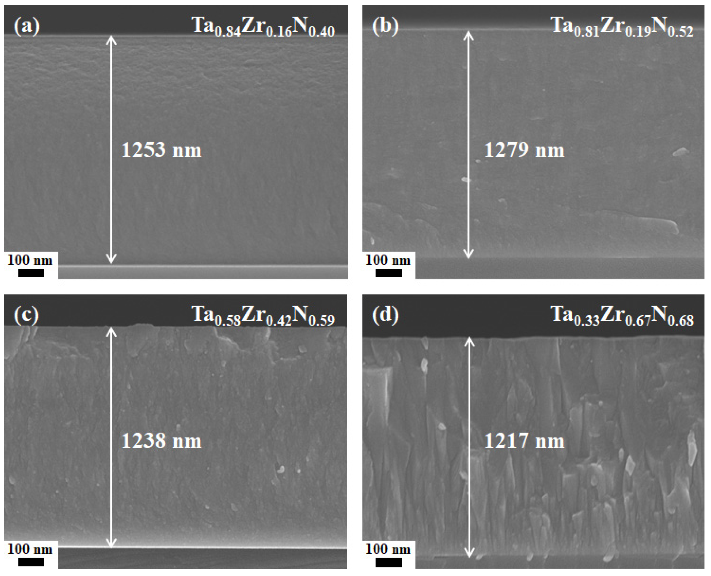
Figure 5.
XRD patterns of the Ta–Zr–N thin films after annealing at 600 °C in 15 ppm O2-N2 for 8 h.
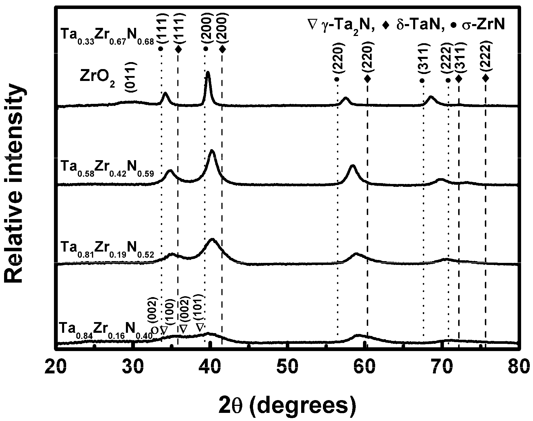
Figure 6.
Cross-sectional SEM images of the Ta–Zr–N thin films after annealing at 600 °C in 15 ppm O2-N2 for 8 h. (a) Ta0.84Zr0.16N0.40; (b) Ta0.81Zr0.19N0.52; (c) Ta0.58Zr0.42N0.59; (d) Ta0.33Zr0.67N0.68.
Figure 6.
Cross-sectional SEM images of the Ta–Zr–N thin films after annealing at 600 °C in 15 ppm O2-N2 for 8 h. (a) Ta0.84Zr0.16N0.40; (b) Ta0.81Zr0.19N0.52; (c) Ta0.58Zr0.42N0.59; (d) Ta0.33Zr0.67N0.68.
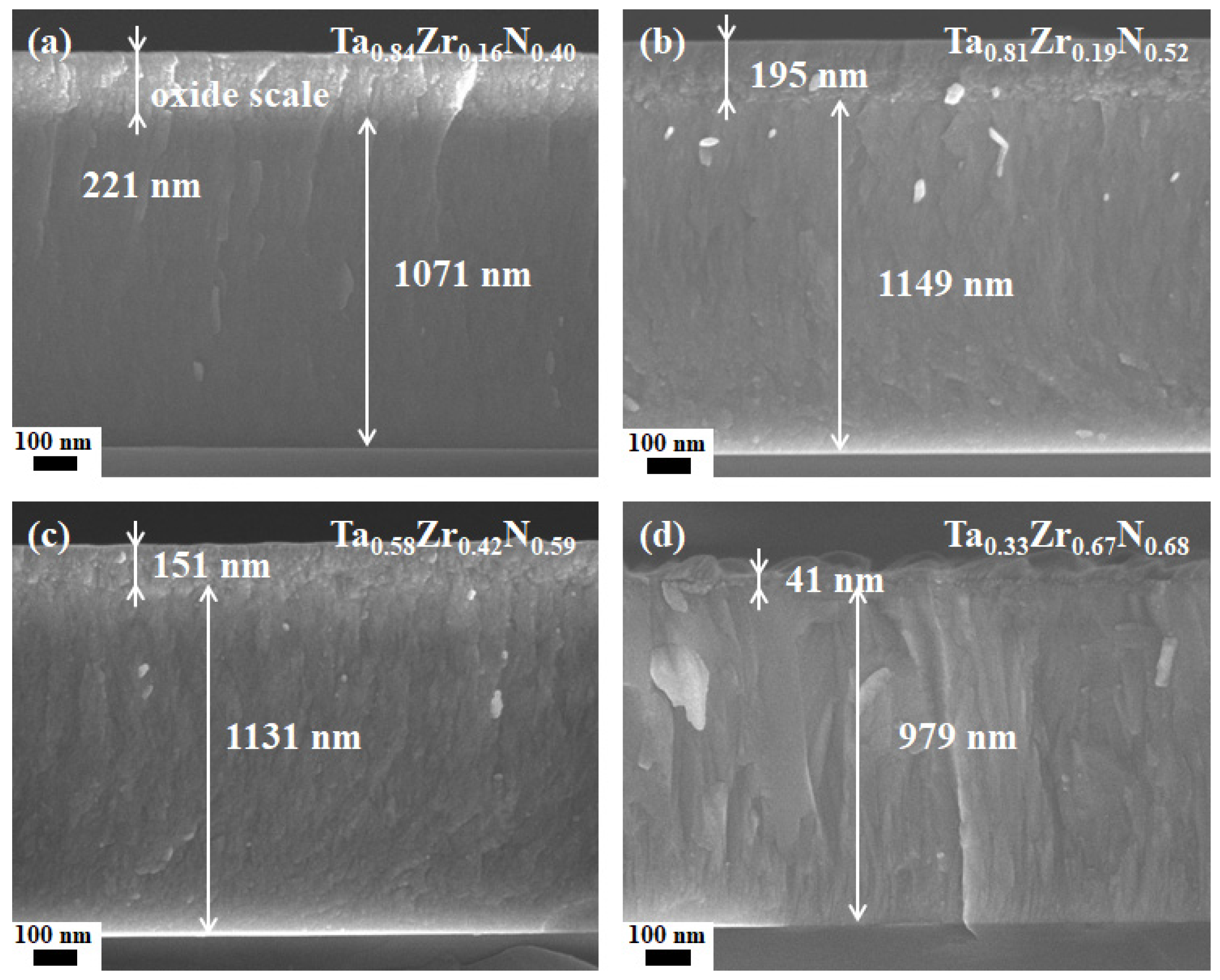
Figure 7.
(a) Cross-sectional TEM image of the Ta0.58Zr0.42N0.59 thin film after annealing at 600 °C in 15 ppm O2-N2 for 8 h; (b) high-resolution image of the outermost surface region; and (c) dark-field image corresponding to the (111) diffraction spot.
Figure 7.
(a) Cross-sectional TEM image of the Ta0.58Zr0.42N0.59 thin film after annealing at 600 °C in 15 ppm O2-N2 for 8 h; (b) high-resolution image of the outermost surface region; and (c) dark-field image corresponding to the (111) diffraction spot.
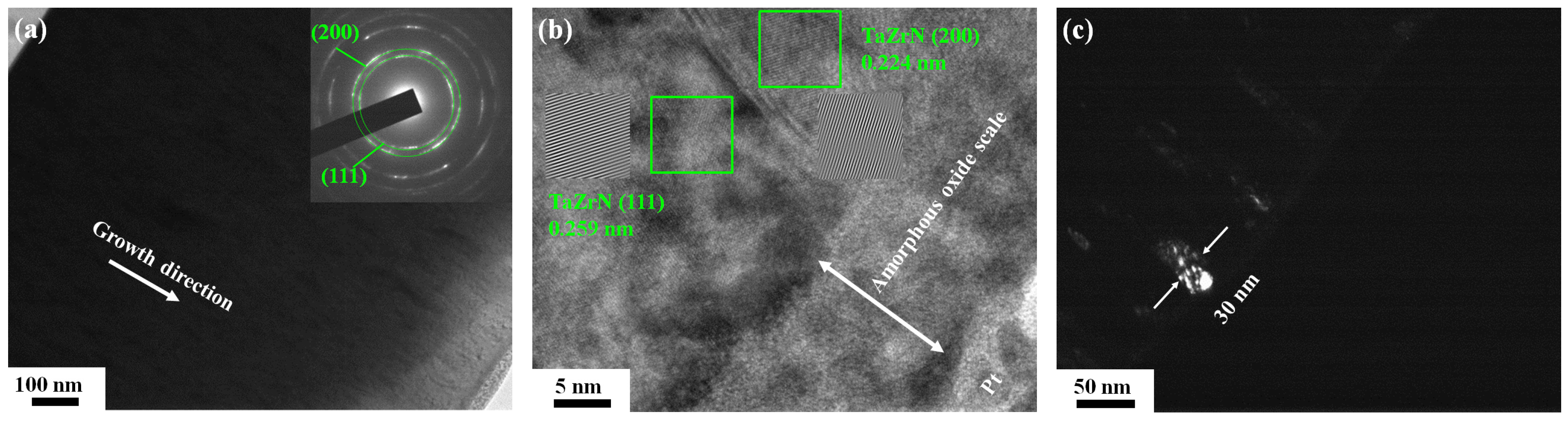
Figure 8.
(a) Cross-sectional TEM image of the Ta0.33Zr0.67N0.68 thin film after annealing at 600 °C in 15 ppm O2-N2 for 8 h; (b) high-resolution image of the near-surface region; and (c) dark-field image corresponding to the (111) diffraction spot.
Figure 8.
(a) Cross-sectional TEM image of the Ta0.33Zr0.67N0.68 thin film after annealing at 600 °C in 15 ppm O2-N2 for 8 h; (b) high-resolution image of the near-surface region; and (c) dark-field image corresponding to the (111) diffraction spot.


Table 1.
Sputter parameters for depositing Ta–Zr–N thin films.
| Sample | RF Power WTa | HIPIMS Power WZr | Zr Power Density (W/cm2) | Deposition Time (min) | Coating Thickness (nm) | Deposition Rate (nm/min) |
|---|---|---|---|---|---|---|
| A | 100 | 400 | 1656 | 210 | 1217 | 5.80 |
| B | 200 | 400 | 1632 | 140 | 1238 | 8.84 |
| C | 300 | 400 | 1576 | 105 | 1279 | 12.18 |
| D | 400 | 400 | 1500 | 85 | 1253 | 14.75 |
Table 2.
Chemical compositions of as-deposited and 600 °C-annealed Ta–Zr–N thin films.
| Sample | Annealing Time (h) | Chemical Composition (at %) | Atomic Ratio | ||||
|---|---|---|---|---|---|---|---|
| Ta | Zr | N | O | Zr/(Ta + Zr) | N/(Ta + Zr) | ||
| A Ta0.33Zr0.67N0.68 | 0 | 19.0 ± 0.0 | 39.1 ± 0.5 | 39.6 ± 0.2 | 2.3 ± 0.2 | 0.67 | 0.68 |
| 4 | 17.5 ± 0.4 | 35.9 ± 0.3 | 34.0 ± 0.7 | 12.6 ± 1.0 | 0.67 | 0.64 | |
| 8 | 16.3 ± 0.4 | 33.6 ± 0.5 | 30.9 ± 0.3 | 19.2 ± 1.3 | 0.67 | 0.62 | |
| B Ta0.58Zr0.42N0.59 | 0 | 36.3 ± 0.1 | 26.1 ± 0.2 | 36.6 ± 0.1 | 1.0 ± 0.0 | 0.42 | 0.59 |
| 4 | 29.3 ± 0.5 | 23.0 ± 0.8 | 28.2 ± 0.5 | 19.5 ± 1.5 | 0.44 | 0.54 | |
| 8 | 27.5 ± 0.5 | 21.8 ± 0.1 | 26.8 ± 0.3 | 23.9 ± 0.3 | 0.44 | 0.54 | |
| C Ta0.81Zr0.19N0.52 | 0 | 52.5 ± 0.2 | 12.5 ± 0.7 | 33.5 ± 0.2 | 1.5 ± 0.3 | 0.19 | 0.52 |
| 4 | 35.8 ± 0.4 | 16.1 ± 0.4 | 24.1 ± 0.0 | 24.0 ± 0.3 | 0.31 | 0.46 | |
| 8 | 33.0 ± 0.3 | 14.9 ± 0.3 | 22.7 ± 0.3 | 29.4 ± 0.3 | 0.31 | 0.47 | |
| D Ta0.84Zr0.16N0.40 | 0 | 59.3 ± 0.7 | 11.0 ± 0.2 | 28.3 ± 0.8 | 1.4 ± 0.1 | 0.16 | 0.40 |
| 4 | 36.3 ± 0.5 | 11.1 ± 0.8 | 20.5 ± 0.2 | 32.1 ± 0.3 | 0.23 | 0.43 | |
| 8 | 35.3 ± 0.7 | 11.1 ± 0.2 | 18.8 ± 0.3 | 34.8 ± 0.6 | 0.24 | 0.41 | |
Table 3.
Film and oxide scale thicknesses, surface roughness, mechanical properties, elastic recovery, and residual stress values of as-deposited and 600 °C-annealed Ta–Zr–N thin films prepared on Si substrates.
Table 3.
Film and oxide scale thicknesses, surface roughness, mechanical properties, elastic recovery, and residual stress values of as-deposited and 600 °C-annealed Ta–Zr–N thin films prepared on Si substrates.
| Sample | TA (h) | Thickness | Surface | H | E | H3/E2 | We | Residual | |
|---|---|---|---|---|---|---|---|---|---|
| Film | Oxide | Roughness | Stress | ||||||
| (nm) | (nm) | (nm) | (GPa) | (GPa) | (GPa) | % | (GPa) | ||
| Ta0.33Zr0.67N0.68 | 0 | 1217 | 0 | 2.54 ± 0.01 | 30.2 ± 0.9 | 306 ± 7 | 0.30 | 67 | −4.18 ± 0.04 |
| 4 | 1176 | 0 | 2.93 ± 0.02 | 28.3 ± 1.6 | 283 ± 4 | 0.28 | 63 | – | |
| 8 | 979 | 41 | 3.55 ± 0.58 | 19.3 ± 1.6 | 235 ± 7 | 0.13 | 56 | – | |
| Ta0.58Zr0.42N0.59 | 0 | 1238 | 0 | 0.52 ± 0.02 | 35.0 ± 0.6 | 311 ± 3 | 0.44 | 73 | −6.17 ± 0.47 |
| 4 | 1208 | 62 | 0.80 ± 0.00 | 25.7 ± 0.4 | 262 ± 3 | 0.25 | 62 | – | |
| 8 | 1131 | 151 | 1.65 ± 0.28 | 24.8 ± 0.5 | 268 ± 4 | 0.21 | 59 | – | |
| Ta0.81Zr0.19N0.52 | 0 | 1279 | 0 | 0.36 ± 0.06 | 35.5 ± 0.4 | 299 ± 3 | 0.50 | 76 | −4.84 ± 0.04 |
| 4 | 1192 | 136 | 1.06 ± 0.10 | 21.5 ± 0.4 | 254 ± 6 | 0.15 | 56 | −3.46 ± 0.19 | |
| 8 | 1149 | 195 | 1.40 ± 0.24 | 19.5 ± 0.3 | 244 ± 3 | 0.13 | 50 | −2.80 ± 0.01 | |
| Ta0.84Zr0.16N0.40 | 0 | 1253 | 0 | 0.37 ± 0.01 | 31.9 ± 0.8 | 258 ± 11 | 0.49 | 75 | −4.65 ± 0.20 |
| 4 | 1164 | 131 | 0.54 ± 0.02 | 20.9 ± 0.5 | 251 ± 3 | 0.14 | 56 | −2.60 ± 0.17 | |
| 8 | 1071 | 221 | 1.15 ± 0.29 | 18.0 ± 0.3 | 235 ± 2 | 0.11 | 52 | −2.80 ± 0.00 | |
Note: TA: Annealing time.
© 2017 by the authors. Licensee MDPI, Basel, Switzerland. This article is an open access article distributed under the terms and conditions of the Creative Commons Attribution (CC BY) license (http://creativecommons.org/licenses/by/4.0/).
Share and Cite
MDPI and ACS Style
Chang, L.-C.; Chang, C.-Y.; You, Y.-W. Ta–Zr–N Thin Films Fabricated through HIPIMS/RFMS Co-Sputtering. Coatings 2017, 7, 189. https://doi.org/10.3390/coatings7110189
AMA Style
Chang L-C, Chang C-Y, You Y-W. Ta–Zr–N Thin Films Fabricated through HIPIMS/RFMS Co-Sputtering. Coatings. 2017; 7(11):189. https://doi.org/10.3390/coatings7110189
Chicago/Turabian StyleChang, Li-Chun, Ching-Yen Chang, and Ya-Wen You. 2017. "Ta–Zr–N Thin Films Fabricated through HIPIMS/RFMS Co-Sputtering" Coatings 7, no. 11: 189. https://doi.org/10.3390/coatings7110189
Note that from the first issue of 2016, this journal uses article numbers instead of page numbers. See further details here.