
Suppression of Graphene Nucleation by Turning Off Hydrogen Supply Just before Atmospheric Pressure Chemical Vapor Deposition Growth

Graduate School of Engineering, Toyota Technological Institute, 2-12-1 Hisakata, Tempaku, Aichi, Nagoya 468-8511, Japan
*
Author to whom correspondence should be addressed.
Coatings 2017, 7(11), 206; https://doi.org/10.3390/coatings7110206
Submission received: 17 October 2017
/
Revised: 7 November 2017
/
Accepted: 9 November 2017
/
Published: 20 November 2017
(This article belongs to the Special Issue Chemical Vapor Deposition)
Abstract
:To exploit the extraordinary property of graphene in practical electrical and optical devices, it is necessary to produce large-sized, single-crystal graphene. Atmospheric pressure chemical vapor deposition (APCVD) on polycrystalline Cu surface is a promising scalable route of graphene synthesis but the unavoidable multiple nucleation limits their reachable domain size. Here, we report that effective suppression of nucleation was achieved by only turning off hydrogen supply before introduction of the carbon source for graphene growth. The density of graphene decreased from 72.0 to 2.2 domains/cm2 by turning off hydrogen for 15 min. X-ray photoelectron spectroscopy and Raman spectroscopy studies show that the Cu surface was covered with 3–4 nm thick highly crystalline Cu2O, which would be caused by oxidation by residual oxidative gasses in the chamber during the turning off period. It was also revealed that elevating the temperature in Ar followed by annealing in H2/Ar before turning off hydrogen led to the enlargement of the Cu domain, resulting in the further suppression of nucleation. By optimizing such growth parameters in the CVD process, a single-crystal graphene with ~2.6 mm in diameter was successfully obtained.
1. Introduction
Graphene is an atomic sheet of carbon atoms densely packed in a honeycomb structure and has attracted plenty of attention [1,2,3]. The extraordinary performance of graphene in optoelectronic and electronic applications has been shown by theoretical and experimental investigations using mechanically exfoliated graphene [4,5,6]. However, the mechanical exfoliation method has no controllability for the flake size and the layer number of graphene, limiting the practical use. A promising scalable route of graphene synthesis is chemical vapor deposition (CVD) on catalytic metal surfaces (Cu [7,8,9,10,11,12,13,14,15], Ni [14,15,16,17], Pt [18], Ir [19], and Ru [20]). Among these, Cu has prominent advantages in terms of cost of production and the preference formation of a single layer originating from the low solubility of carbon [14]. However, the grown CVD graphene is generally polycrystalline [10,21], and its domain boundaries degrade electronic properties such as carrier mobility [22]. Thus, the growth of large-sized graphene with a single crystal domain is highly needed for practical graphene applications.
A strategy to obtain such a large-sized crystal domain is to reduce the nucleation density of graphene. The nucleation density is strongly affected by the amount of carbon supply during the graphene growth [10,23,24] and the number of active sites for graphene nucleation [25,26]. As for the carbon supply, a reduced supply of carbon sources is required to achieve the effective suppression of nucleation [10,23]. In the latter aspect, atomic steps, point defects, impurities, and the grain boundaries on the Cu surface may act as the potential nucleation sites [26,27]. Many approaches have been performed to reduce the active sites by pretreatment of Cu [13,28], resulting in the growth of millimeter-size single crystal graphene [11,23,24,29,30]. Further increase of domain size was demonstrated by utilizing oxygen in the CVD process. Gan et al. reported that oxygen plays a role to control nucleation seeds in the preheating process, giving subcentimeter single-crystal by controlling the seeding process [31]. Hao et al. reported that surface oxygen plays roles in the passivation of active sites as well as in the acceleration of domain growth by reducing the attachment barrier of carbon to the edge of the domain, resulting in a centimeter single-crystal [32].
Although the technique to grow a large-sized graphene has been steadily advanced, further enlargement in the domain size is desirable for practical use. In addition, the wide variation in domain size, shape, density, and film quality from lab to lab suggests that the growth mechanism of graphene has not been comprehensively understood. Therefore, effective and reproducible methods for suppressing nucleation should be established with understanding of the growth mechanism. Here, we report that the effective suppression of nucleation can be achieved by only turning off hydrogen supply before the introduction of the carbon source for graphene, resulting in the growth of single crystal graphene up to 2.6 mm. The effect of the Ar annealing to the physical property of the substrate surface was studied by depth-profiling X-ray photoelectron spectroscopy (XPS) and Raman spectroscopy. It was revealed that a very thin Cu2O (3–4 nm thick) layer was formed after the Ar annealing, suggesting the existence of residual oxidative gasses such as oxygen and water vapor in the CVD chamber. The present report proposes the utilization of the residual oxidative gasses for large size graphene growth, and clarifies the reason for the wide variation in graphene growth from lab to lab. It was also revealed that elevating temperature in the Ar followed by annealing in H2/Ar before turning off hydrogen led to enlargement of the Cu domain, resulting in further suppression of nucleation. The present APCVD process neither requires any special gasses, high quality Cu foils, nor vacuum pumps, which is ideal for mass production of large single crystal graphenes at a low cost.
2. Materials and Methods
The APCVD system for graphene growth consists of an inner 30 mm and outer 36 mm diameter quartz tubes as a sample holder and a chamber, respectively (Figure 1a). The purities of H2 and Ar gasses are higher than 99.99999% (7N), and 99.9999% (6N), respectively. The chamber pressure has been kept at a slightly higher pressure than atmospheric pressure (0.123–0.128 MPa) during the CVD process. Commercially available 100 μm thick Cu foils (#113321, Nilaco, Tokyo, Japan) with a size of ~2.2 cm × 10 cm were used as catalytic substrates for the growth.
The concentration of residual oxygen in the CVD chamber under Ar flow was measured by a zirconia oxygen sensor (LC-750 L, Toray Engineering, Tokyo, Japan). The zirconia oxygen sensor was placed downstream of the heating furnace. Optical microscopy (Digital Microscope VHX-5000, Keyence, Osaka, Japan) and field emission scanning electron microscopy (S4700, Hitachi High-Technologies Corporation, Tokyo, Japan) were used to obtain the density and the size of graphenes. To visualize graphene in the optical image, Cu foils were oxidized in air around 200 °C. Then the graphene nucleation density was measured by counting the amount of graphene in an optical microscope image. The average nucleation densities were obtained from several different optical images on the same sample. Surface analysis of Cu foils was performed by XPS (PHI 5000 VersaProbe II, ULVAC-PHI, Kanagawa, Japan) under a base pressure of ~6 × 10⁻⁸ Pa and a monochromatized Al Kα (1486.6 eV) X-ray source. Energy calibration was performed using the position of the primary C 1s peak at 284.8 eV. Atomic concentrations were calculated using the ratio of integrated spectral areas for C1s, O1s, and Cu2p3/2 from high resolution scans and the relative sensitivity factors inherent to the instrument. The accuracy of the atomic concentration is up to 10% of the measured value. Cu foils were sputtered by using accelerated Ar ions with 1 kV for the depth profiling of XPS. The sputtering depth of Cu by 1 kV Ar ions was calibrated by using Cu thin films deposited by vacuum evaporation. We calculated the difference of the expected sputtered depth between low index Cu crystal planes such as (100), (110), and (111) by 1 kV Ar ions as shown in Table S1. As a result, (100) and (111) showed the smallest and the largest depth, and the depth ratio of (100) to (111) is 0.77 to 0.85, indicating that the crystal plane does not largely affect the depths sputtered by 1 kV Ar ions. The transfer from the CVD to the XPS chamber was performed within 10 min to minimize the gradual change of the chemical state of the Cu surface by ambient air and water [33]. Raman microscopy (lnVia Reflex, Renishaw, Gloucestershire, UK) with a 532 nm laser was used to characterize crystal quality of Cu foils and CVD graphene samples.
3. Results and Discussion
A typical CVD process in the present study is schematically shown in Figure 1b. The Cu foil was heated with Ar flow (1000 standard cubic centimeter per minute: (sccm)) until 1000 °C (Ar heating) and with H2/Ar flow (100/500 sccm) until the reaction temperature (1035 °C). The elevation to the reaction temperature from room temperature takes ~50 min. Then the Cu was annealed for 15–45 min with H2/Ar flow (H2/Ar annealing). The hydrogen flow was turned off for 0–20 min before introducing CH4 (Ar annealing). Subsequently, to initiate the growth, the pure Ar flow was replaced by the 10 ppm CH4 diluted in Ar (500–1000 sccm) and the H2 (15–20 sccm). Finally, the CVD chamber was rapidly cooled down to room temperature within 30 min.
Figure 2a–c shows optical microscope images of CVD graphene grown on Cu with different Ar annealing times. The preceding H2/Ar annealing and the subsequent growth time were fixed at 15 and 150 min, respectively. It is obvious that the density of graphene was reduced by increasing the Ar annealing time. Figure 2e shows the dependence of average density of graphene domains on Ar annealing time for two different growth conditions. The numerical values of the average densities of the graphene domains in Figure 2e are summarized in Table S2. Square (corresponding to Figure 2a–c) and circle plots in Figure 2e correspond to 15/500 and 15/1000 for the gas flow ratios of H2 and diluted CH4 in Ar (H2/CH4) during the growth. The density of graphene decreased rapidly with increasing Ar annealing time for both growth conditions (Figure 2e). For instance, the density of graphene decreased from 72.0 to 2.2 domains/cm2 by 15-min Ar annealing for the H2/CH4 of 15/1000. The decrease in the density of graphenes implies that the Ar annealing is effective for suppressing graphene nucleation. Figure 2d shows an optical microscope image of CVD graphene grown after longer annealing in H2/Ar for 45 min without Ar annealing. Since the density of graphene in Figure 2c is smaller than that in Figure 2d, Ar annealing is more effective for suppressing graphene nucleation than extending H2/Ar annealing time.
In addition, the standard errors in Figure 2e were larger in the gas follow ratio of H2/CH4 of 15/1000 than that of 15/500 (see Table S2). The H2/CH4 of 15/1000 was used for the high speed growth. The large standard errors in Figure 2e indicate that the high speed growth results in a large distribution in density of the graphene domain. The variation of the density of graphene obtained by 15/1000 at different locations can be seen in optical microscope images of graphene/Cu in Figures S1–S3.
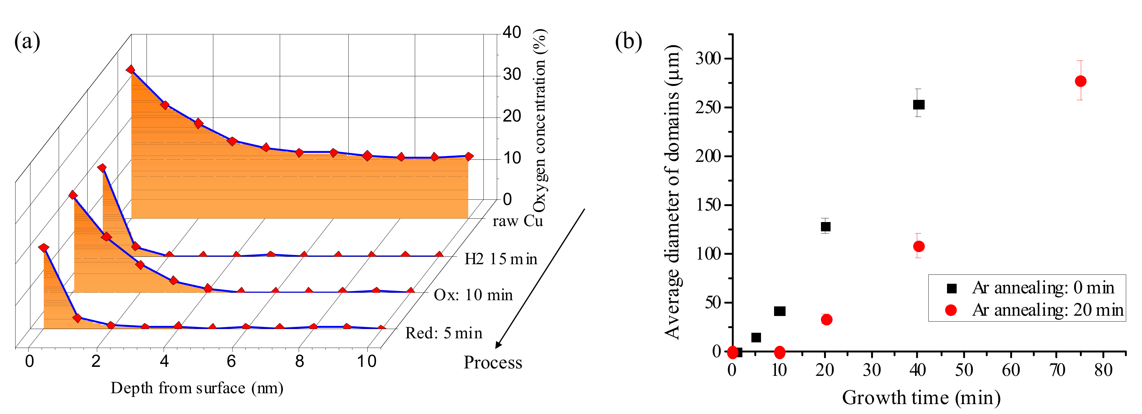
To understand the suppressed nucleation caused by the Ar annealing, we examined annealed Cu surfaces before growth by XPS. The samples were prepared with a fixed H2/Ar annealing time (15 min) and a different Ar annealing time (0–20 min), and were then cooled down under Ar ambient without growth process. Since the Cu surface is easily oxidized in air and the chemical state gradually changes with time [33], we immediately transferred the annealed Cu foils to the XPS chamber to minimize the effect. Figure 3a,b show high-resolution O1s and Cu2p3/2 XPS spectra taken at different depths (0–4 nm) in the 5 min-annealed Cu foil, respectively. In O1s depth profiling (Figure 3a), the major (530.6 eV) and the second peaks (532.1 eV) at 0 nm (black) represent the Cu2O and hydroxyl (OH−) group due to the humidity in ambient, respectively, which is in good agreement with the previous results [33]. The O1s spectra at 1 nm (red online) showed a single peak at 530.3 eV also corresponding to Cu2O as previously reported in the electrodeposited copper oxide film after Ar sputtering [34]. The observed Cu2p3/2 spectra showed a single peak at 932.6 eV for all depths, corresponding to Cu2O [33,35], consistent with O1s spectra. The formation of Cu2O is consistent with the result of Cu LMM which is shown in Figure S4. Figure 3c shows the dependence of oxygen concentrations on the depth from surface of Cu foils with different Ar annealing times. It was found that the oxygen concentration was increased at deeper positions (1–4 nm) by increasing the Ar annealing time. Wrong call-out order.
To find the reason for Cu2O formation during Ar annealing, we measured the oxygen concentration in the CVD chamber under Ar flow. Figure S5a showed the transition of residual oxygen in the CVD chamber. Ar flowing (1000 sccm) and elevating the temperature were started at 0 and 1 min, respectively. The chamber pressure was kept at ~0.12 MPa. The temperature was reached at 1035 °C after 50 min. The chamber pressure was ~0.12 MPa. The oxygen concentration was suddenly decreased after flowing Ar (Figure S5a). When the temperature was reached at 1035 °C, the oxygen concentration showed ~10 ppm. With continuing heating in the Ar, the oxygen concentration gradually increased as shown in Figure S5b, which is an enlarged graph of Figure S5a. The oxygen concentration increased to ~4.2 ppm for 20 min after reaching the minimum concentration, which is a typical time for Ar annealing. Thus, the residual oxygen concentration during Ar annealing would be 10–20 ppm.
In the gas-phase reaction, the following equilibrium must be considered for Cu2O formation:
4Cusurface + O2 ⇔ 2Cu2O [36].
Based on thermodynamics, the equilibrium oxygen partial pressure is about 0.1 Pa at 1035 °C [37], which is lower than the partial pressure of the residual oxygen (~1 Pa). Therefore, the residual oxygen can provide surface oxidation to form the Cu2O during the Ar annealing. On the other hand, dissociation of Cu2O at the metal oxide interface (Cu2O(s) → 2Cu(s) + O) would also be happening at a high temperature [38,39,40]. In addition, the segregation of oxygen during the cooling process is not likely for the formation of the Cu2O (Figure S6). The observed difference in thickness of the Cu2O in Figure 3c and Figure S7b would imply that surface oxidation is faster than the dissociation of the oxide during the Ar annealing.
To clarify the crystal structure of the Cu2O layer, Raman spectroscopy was performed for a CVD-treated Cu foil with Ar annealing for 20 min (H2/Ar annealing and growth for 45 and 150 min, respectively). However, any peaks of Cu2O were not observed in the Ar-annealed Cu foil since the thickness of the Cu2O layer is too thin to detect by Raman spectroscopy. To gain Raman signals, the CVD-treated Cu foil was intentionally oxidized at ~200 °C for 3 min in air (Oxi-CVD), and was measured by Raman spectroscopy. The thickness of the oxide layer was more than 100 nm which was confirmed by XPS depth profiling. To compare Raman spectra, an oxidized as-received Cu foil was also prepared (Oxi-foil).
Figure 4a shows Raman spectra of the Oxi-foil (red) and the Oxi-CVD (blue). All peaks in Figure 4a can be assigned to the phonon energies of Cu2O: (i) (90 cm−1) and (110 cm−1), which are silent modes [41,42]; (150 cm−1) and (TO (625 cm−1) and LO (648 cm−1)), which are infrared active [41,42]; (iii) (521 cm−1), which is the Raman-active mode [41,42]; (IV) (217 cm−1) [42] and (300 cm−1) [43], which are an overtone and combination of them. The appearances of modes and are derived from the activation by defects or resonance effects [41,44,45]. Thus, the Cu2O formation by oxidation in the air was clearly observed and detectable by Raman spectroscopy for both the Oxi-CVD and Oxi-foil. Figure 4b shows high resolution Raman spectra around the intense peaks of and modes. Table 1 summarizes peak positions and the full width at half maximum (FWHM) of these peaks for the Oxi-CVD and Oxi-foil samples. These statistical data were extracted from 36 Raman spectra with peaks fitted by a mixture of Lorentzian and Gaussian functions. The peak positions of and modes in the Oxi-CVD are nearly the same as that of Oxi-foil. On the other hand, the FWHM of and modes in the Oxi-CVD were smaller than that of the Oxi-foil, indicating the higher crystallinity of Cu2O in Oxi-CVD, as reported by Solache-Carranco et al. [46]. This result indicated that the present Ar annealing formed a Cu2O thin layer with high crystallinity.
Figure S8a,b is a representative SEM image and electron backscatter diffraction (EBSD) orientation map of a Cu surface which was heated at elevated temperatures in Ar following by H2/Ar annealing for 2.5 h. The color in Figure S8b represents the fcc crystalline orientation of Cu as shown in Figure S8c. Figure S8d is the area ratio of low index faces for the annealed Cu obtained by statistical analysis of EBSD orientation maps such as Figure S8b. The major crystal face of Cu is (111), and the second (001) as shown in Figure S8b. It is reported that the oxidation of Cu (111) and Cu (001) results in epitaxial Cu2O [47]. Therefore, the Cu2O formed by the present Ar annealing would be mainly (111) and (001) surfaces.
To gain full understanding of the evolution of the chemical states of the Cu surface, XPS depth profile measurement was performed on Cu foils which were cooled down after a specific CVD process. These Cu foils are “raw Cu”, “H2: 15 min”, “Ox: 10 min”, and “Red: 5 min” corresponding to the timing of #1–4 shown in Figure 1b, respectively. Figure 5a shows the evolution of the depth profile of oxygen in Cu foils by the CVD process. It was found that the “raw Cu” contains abundant oxygen inside the foil. The oxygen signals in the “H2: 15 min” and “Red: 5 min” samples disappeared around 2 nm in depth. Since the oxygen near the surface would come from native oxide formed during the transferring of the sample, the surface of “H2: 15 min” and “Red: 5 min” samples would be completely reduced to the metallic Cu. The “Ox: 10 min” sample showed detectable oxygen signals until 4 nm from surface, being consistent with Figure 3c.
In addition, the initial growth behavior of graphene has been examined. Figure 5b shows a dependence of the average diameter of the graphene domain on growth time for the substrates without and with 20 min annealing in Ar. Incubation times were observed of around 1 and 10 min for the CVD samples with the 0 and 20 min-Ar annealing, respectively. This indicates that the nucleation of graphene is delayed by the existence of a Cu2O layer, probably due to the less catalytic activity of Cu2O for decomposing CH4.
Although we revealed that surface oxidation by Ar annealing is an efficient way to reduce the density of the nucleation of graphene, the role of Ar heating and H2/Ar annealing before Ar annealing remains unclear. To reveal them, the graphene was grown with a fixed Ar annealing time (20 min) after heating and annealing (15 min) in H2/Ar or Ar ambient, and the density of graphene and the morphology of Cu were compared to the present process (Ar heating and H2/Ar annealing followed by Ar annealing). Figure 6a–f show high and low magnification optical microscope images of CVD graphene obtained by Ar heating followed by H2/Ar annealing (Figure 6a,d), heating and annealing in H2/Ar (Figure 6b,e), and heating and annealing in Ar (Figure 6c,f). It can be seen that the present Ar heating followed by H2/Ar annealing (Figure 6a) provided the largest domain of Cu, and the lowest density of graphene among these processes, proving the present process is the best condition of the heating and annealing process. Since the surface oxidation condition (Ar annealing for 20 min) were the same for all samples in Figure 6, the reduction of the graphene density in the present heating and annealing was mainly caused by lowering the number of domain boundaries of Cu, which are active sites for graphene nucleation [26]. On the other hand, the other two processes did not provide the largest domain size of Cu, indicating that the solely H2/Ar or Ar annealing is not an effective way to form a large domain of Cu. Although the detailed mechanism of the large domain formation of Cu is not clear, it would be related to Cu transport, which can be changed by the chemisorption of oxygen [48,49]. The present Ar heating followed by H2/Ar annealing would provide higher mobility of Cu atoms, and resulted in large size Cu domains.
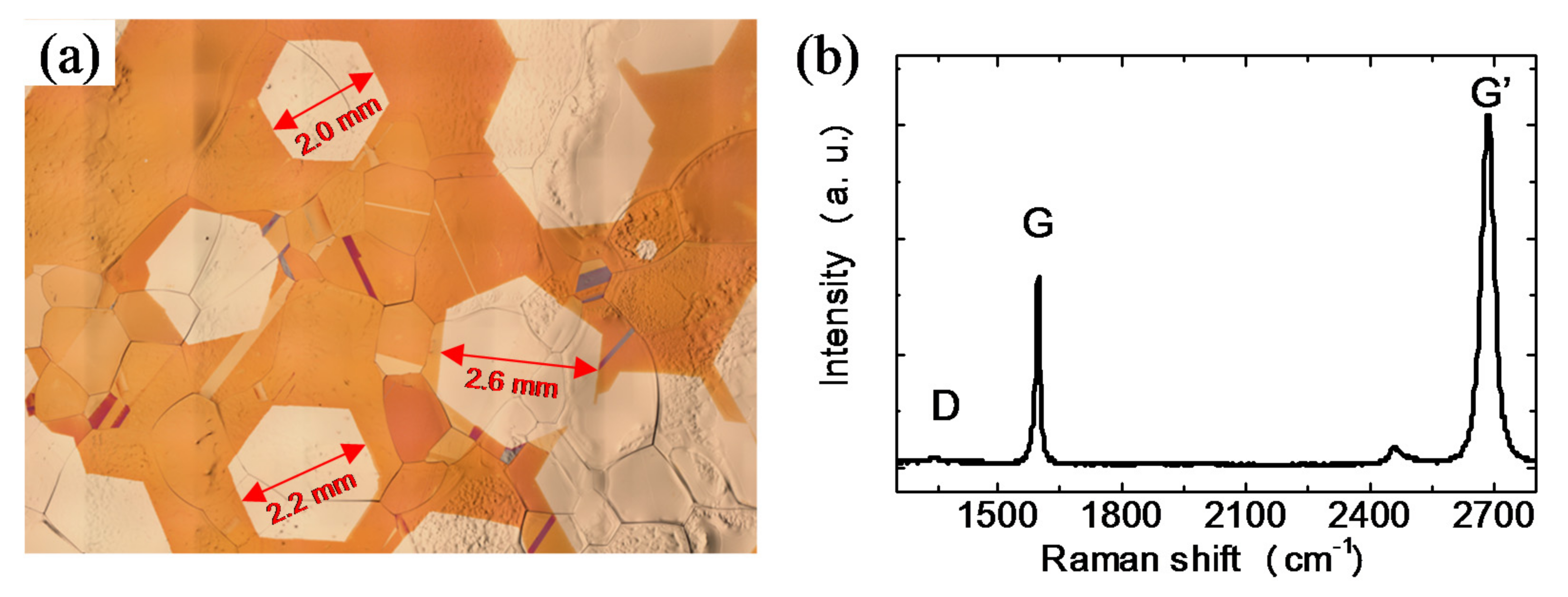
Figure 7a shows an optical microscope image of large-sized graphene domains by a CVD process with the H2/Ar and the Ar annealing for 100 and 35 min, respectively. The isolated hexagonal shape in Figure 7a corresponds to a single crystal domain of graphene [12,23], and single crystal with a size of up to 2.6 mm in diameter was obtained. The single crystallinity of the hexagonal domain was also experimentally confirmed by low-energy electron diffraction (LEED) pattern (Figure S9). Figure 7b shows a Raman spectrum of a millimeter scale CVD graphene transferred to a SiO2/Si substrate, where G’, G, and D peaks were observed around 2685, 1590, and 1345 cm−1, respectively. The higher intensity of G’ than G and negligible small D peak indicated the single layer formation and high quality crystallinity of the graphene, respectively [50,51,52]. Thus, the present modified CVD process successfully demonstrated a large-sized, single-layer graphene formation with high quality.
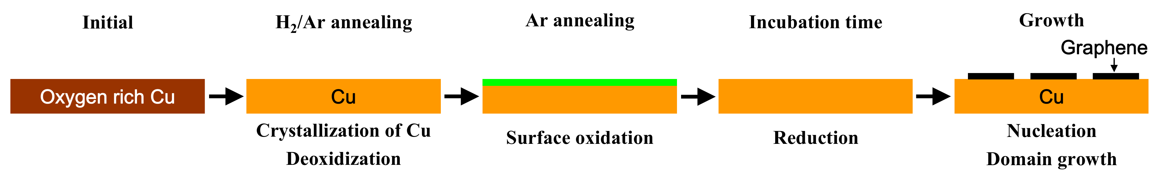
From the aforementioned results, the evolution of the Cu surface is schematically summarized in Figure 8. At the beginning, the as-received Cu foil has abundant oxygen inside Cu (“Initial” in Figure 8, and #1 in Figure 1b). During H2/Ar annealing at 1035 °C for 15 min, the oxygen concentration in the Cu suddenly decreases and the crystallization of Cu occurs (“H2/Ar annealing” in Figure 8, and #2 in Figure 1b). Subsequent Ar annealing provides surface oxidation (“Ar annealing” in Figure 8, and #3 in Figure 1b). The thin layer Cu2O formed by Ar annealing has high crystallinity since it was formed on crystalline Cu, as observed by Raman spectroscopy (Figure 4 and Table 1). After the initiation of the growth process, the reduction of the surface is started again due to the presence of H2, and is completed within 5 min (“Incubation time” in Figure 8, and #4 in Figure 1b). Finally, the nucleation of graphene occurs after the supersaturation of active carbons [8], and then domain growth is started (“Growth” in Figure 8).
The most important process for suppressing nucleation is Ar annealing, which provides surface oxidation. The surface oxidation was reported to remove carbon impurities [53,54] and to passivate active sites [32], resulting in suppressed graphene nucleation. The removal of carbon impurities happens not only from the surface, but also in the bulk Cu through the dissociation of Cu2O and the diffusion of dissolved atomic oxygen [54]. The highly crystalline Cu2O observed in the present study may also be attributed to the passivation of active sites, since structural defects in the preformed Cu2O layer would not possess a sufficient passivation effect. By prolonged Ar annealing, both the removal of carbon impurities and the passivation effects are enhanced, resulting in suppressed graphene nucleation. In addition, Ar heating followed by H2/Ar annealing contributes to the enlargement of the Cu domain, resulting in the additional suppression of nucleation by reducing active sites such as domain boundaries of Cu.
4. Conclusions
We investigated the effect of turning off hydrogen (Ar annealing) before the growth process on Cu, and engineered it for large size graphene growth. We first revealed that the Ar annealing oxidizes the Cu surface by residual oxidant, which results in the effective suppression of graphene nucleation. The enlargement of the Cu domain by Ar heating, followed by H2/Ar annealing before Ar annealing was ascribed to the extra suppression of graphene nucleation. Finally, single crystal graphene of ~2.6 mm diameter was successfully grown by utilizing the Ar annealing. This study demonstrated that a large-sized single crystal graphene can be grown by utilizing oxidative gasses in the CVD chamber. We expect that the existence of the oxidative gasses is one of the reasons for the wide variation in graphene growth from lab to lab. It is also noted that our modified APCVD process requires neither vacuum pumps nor high-quality Cu, and it is compatible for industrial scale mass production of large-sized single crystal graphene.
Supplementary Materials
Supplementary materials are available online at https://www.mdpi.com/2079-6412/7/11/206/s1.
Acknowledgments
The authors thank Yoshimi Horio at Daido University for his help with the LEED measurements. This work was supported in part by the Grant-in-Aid for Young Scientist (Start-up) (No. 15H06723), Research Center for Green Electronic Devices and Materials (S1411027), and Strategic Research Foundation Grant-aided Project for Private Universities from the Ministry of Education, Culture, Sport, Science, and Technology, Japan (MEXT).
Author Contributions
Seiya Suzuki conceived, designed, and performed the experiments; Yoshifumi Terada provided primitive important experiments for the paper. Masamichi Yoshimura contributed reagents/materials/analysis tools; Seiya Suzuki wrote the paper. Masamichi Yoshimura contributed revision and collection of the paper.
Conflicts of Interest
The authors declare no conflict of interest.
References
- Geim, A.K.; Novoselov, K.S. The rise of graphene. Nat. Mater. 2007, 6, 183–191. [Google Scholar] [CrossRef] [PubMed]
- Novoselov, K.; Geim, A.K.; Morozov, S.; Jiang, D.; Katsnelson, M.; Grigorieva, I.; Dubonos, S.; Firsov, A. Two-dimensional gas of massless Dirac fermions in graphene. Nature 2005, 438, 197–200. [Google Scholar] [CrossRef] [PubMed] [Green Version]
- Zhang, Y.; Tan, Y.-W.; Stormer, H.L.; Kim, P. Experimental observation of the quantum Hall effect and Berry’s phase in graphene. Nature 2005, 438, 201–204. [Google Scholar] [CrossRef]
- Xia, F.; Mueller, T.; Lin, Y.-M.; Valdes-Garcia, A.; Avouris, P. Ultrafast graphene photodetector. Nat. Nanotechnol. 2009, 4, 839–843. [Google Scholar] [CrossRef] [PubMed]
- Liu, M.; Yin, X.; Ulin-Avila, E.; Geng, B.; Zentgraf, T.; Ju, L.; Wang, F.; Zhang, X. A graphene-based broadband optical modulator. Nature 2011, 474, 64–67. [Google Scholar] [CrossRef] [PubMed]
- Wilmart, Q.; Berrada, S.; Torrin, D.; Nguyen, V.H.; Fève, G.; Berroir, J.-M.; Dollfus, P.; Plaçais, B. A Klein-tunneling transistor with ballistic graphene. 2D Mater. 2014, 1, 011006. [Google Scholar] [CrossRef]
- Bae, S.; Kim, H.; Lee, Y.; Xu, X.; Park, J.-S.; Zheng, Y.; Balakrishnan, J.; Lei, T.; Kim, H.R.; Song, Y.I. Roll-to-roll production of 30-inch graphene films for transparent electrodes. Nat. Nanotechnol. 2010, 5, 574–578. [Google Scholar] [CrossRef] [PubMed]
- Kim, H.; Mattevi, C.; Calvo, M.R.; Oberg, J.C.; Artiglia, L.; Agnoli, S.; Hirjibehedin, C.F.; Chhowalla, M.; Saiz, E. Activation energy paths for graphene nucleation and growth on Cu. ACS Nano 2012, 6, 3614–3623. [Google Scholar] [CrossRef] [PubMed]
- Li, X.; Cai, W.; An, J.; Kim, S.; Nah, J.; Yang, D.; Piner, R.; Velamakanni, A.; Jung, I.; Tutuc, E. Large-area synthesis of high-quality and uniform graphene films on copper foils. Science 2009, 324, 1312–1314. [Google Scholar] [CrossRef] [PubMed]
- Li, X.; Magnuson, C.W.; Venugopal, A.; An, J.; Suk, J.W.; Han, B.; Borysiak, M.; Cai, W.; Velamakanni, A.; Zhu, Y. Graphene films with large domain size by a two-step chemical vapor deposition process. Nano Lett. 2010, 10, 4328–4334. [Google Scholar] [CrossRef] [PubMed]
- Li, X.; Magnuson, C.W.; Venugopal, A.; Tromp, R.M.; Hannon, J.B.; Vogel, E.M.; Colombo, L.; Ruoff, R.S. Large-area graphene single crystals grown by low-pressure chemical vapor deposition of methane on copper. J. Am. Chem. Soc. 2011, 133, 2816–2819. [Google Scholar] [CrossRef] [PubMed]
- Vlassiouk, I.; Regmi, M.; Fulvio, P.; Dai, S.; Datskos, P.; Eres, G.; Smirnov, S. Role of hydrogen in chemical vapor deposition growth of large single-crystal graphene. ACS Nano 2011, 5, 6069–6076. [Google Scholar] [CrossRef] [PubMed]
- Wang, H.; Wang, G.; Bao, P.; Yang, S.; Zhu, W.; Xie, X.; Zhang, W.-J. Controllable synthesis of submillimeter single-crystal monolayer graphene domains on copper foils by suppressing nucleation. J. Am. Chem. Soc. 2012, 134, 3627–3630. [Google Scholar] [CrossRef] [PubMed]
- Li, X.; Cai, W.; Colombo, L.; Ruoff, R.S. Evolution of graphene growth on Ni and Cu by carbon isotope labeling. Nano Lett. 2009, 9, 4268–4272. [Google Scholar] [CrossRef] [PubMed]
- Sun, Z.; Yan, Z.; Yao, J.; Beitler, E.; Zhu, Y.; Tour, J.M. Growth of graphene from solid carbon sources. Nature 2010, 468, 549–552. [Google Scholar] [CrossRef] [PubMed]
- Kim, K.S.; Zhao, Y.; Jang, H.; Lee, S.Y.; Kim, J.M.; Kim, K.S.; Ahn, J.-H.; Kim, P.; Choi, J.-Y.; Hong, B.H. Large-scale pattern growth of graphene films for stretchable transparent electrodes. Nature 2009, 457, 706–710. [Google Scholar] [CrossRef] [PubMed]
- Reina, A.; Jia, X.; Ho, J.; Nezich, D.; Son, H.; Bulovic, V.; Dresselhaus, M.S.; Kong, J. Large area, few-layer graphene films on arbitrary substrates by chemical vapor deposition. Nano Lett. 2009, 9, 30–35. [Google Scholar] [CrossRef] [PubMed]
- Gao, L.; Ren, W.; Xu, H.; Jin, L.; Wang, Z.; Ma, T.; Ma, L.-P.; Zhang, Z.; Fu, Q.; Peng, L.-M. Repeated growth and bubbling transfer of graphene with millimetre-size single-crystal grains using platinum. Nat. Commun. 2012, 3, 699. [Google Scholar] [CrossRef] [PubMed]
- Pletikosić, I.; Kralj, M.; Pervan, P.; Brako, R.; Coraux, J.; N’diaye, A.; Busse, C.; Michely, T. Dirac cones and minigaps for graphene on Ir (111). Phys. Rev. Lett. 2009, 102, 056808. [Google Scholar] [CrossRef] [PubMed]
- Sutter, P.W.; Flege, J.-I.; Sutter, E.A. Epitaxial graphene on ruthenium. Nat. Mater. 2008, 7, 406–411. [Google Scholar] [CrossRef] [PubMed]
- Huang, P.Y.; Ruiz-Vargas, C.S.; van der Zande, A.M.; Whitney, W.S.; Levendorf, M.P.; Kevek, J.W.; Garg, S.; Alden, J.S.; Hustedt, C.J.; Zhu, Y. Grains and grain boundaries in single-layer graphene atomic patchwork quilts. Nature 2011, 469, 389–392. [Google Scholar] [CrossRef] [PubMed]
- Yu, Q.; Jauregui, L.A.; Wu, W.; Colby, R.; Tian, J.; Su, Z.; Cao, H.; Liu, Z.; Pandey, D.; Wei, D. Control and characterization of individual grains and grain boundaries in graphene grown by chemical vapour deposition. Nat. Mater. 2011, 10, 443–449. [Google Scholar] [CrossRef] [PubMed]
- Yan, Z.; Lin, J.; Peng, Z.; Sun, Z.; Zhu, Y.; Li, L.; Xiang, C.; Samuel, E.L.; Kittrell, C.; Tour, J.M. Toward the synthesis of wafer-scale single-crystal graphene on copper foils. ACS Nano 2012, 6, 9110–9117. [Google Scholar] [CrossRef] [PubMed]
- Zhang, Y.; Chen, Z.; Wang, B.; Wu, Y.; Jin, Z.; Liu, X.; Yu, G. Controllable growth of millimeter-size graphene domains on cu foil. Mater. Lett. 2013, 96, 149–151. [Google Scholar] [CrossRef]
- Lin, L.; Li, J.; Ren, H.; Koh, A.L.; Kang, N.; Peng, H.; Xu, H.; Liu, Z. Surface engineering of copper foils for growing centimeter-sized single-crystalline graphene. ACS Nano 2016, 10, 2922–2929. [Google Scholar] [CrossRef] [PubMed]
- Han, G.H.; Güneş, F.; Bae, J.J.; Kim, E.S.; Chae, S.J.; Shin, H.-J.; Choi, J.-Y.; Pribat, D.; Lee, Y.H. Influence of copper morphology in forming nucleation seeds for graphene growth. Nano Lett. 2011, 11, 4144–4148. [Google Scholar] [CrossRef] [PubMed]
- Kim, S.M.; Hsu, A.; Lee, Y.-H.; Dresselhaus, M.; Palacios, T.; Kim, K.K.; Kong, J. The effect of copper pre-cleaning on graphene synthesis. Nanotechnology 2013, 24, 365602. [Google Scholar] [CrossRef] [PubMed]
- Suzuki, S.; Nagamori, T.; Matsuoka, Y.; Yoshimura, M. Threefold atmospheric-pressure annealing for suppressing graphene nucleation on copper in chemical vapor deposition. Jpn. J. Appl. Phys. 2014, 53, 095101. [Google Scholar] [CrossRef]
- Chen, S.; Ji, H.; Chou, H.; Li, Q.; Li, H.; Suk, J.W.; Piner, R.; Liao, L.; Cai, W.; Ruoff, R.S. Millimeter-size single-crystal graphene by suppressing evaporative loss of cu during low pressure chemical vapor deposition. Adv. Mater. 2013, 25, 2062–2065. [Google Scholar] [CrossRef] [PubMed]
- Suzuki, S.; Kiyosumi, K.; Nagamori, T.; Tanaka, K.; Yoshimura, M. Low density growth of graphene by air introduction in atmospheric pressure chemical vapor deposition. e-J. Surf. Sci. Nanotechnol. 2015, 13, 404–409. [Google Scholar] [CrossRef]
- Gan, L.; Luo, Z. Turning off hydrogen to realize seeded growth of subcentimeter single-crystal graphene grains on copper. ACS Nano 2013, 7, 9480–9488. [Google Scholar] [CrossRef] [PubMed]
- Hao, Y.; Bharathi, M.; Wang, L.; Liu, Y.; Chen, H.; Nie, S.; Wang, X.; Chou, H.; Tan, C.; Fallahazad, B. The role of surface oxygen in the growth of large single-crystal graphene on copper. Science 2013, 342, 720–723. [Google Scholar] [CrossRef] [PubMed]
- Platzman, I.; Brener, R.; Haick, H.; Tannenbaum, R. Oxidation of polycrystalline copper thin films at ambient conditions. J. Phys. Chem. C 2008, 112, 1101–1108. [Google Scholar] [CrossRef]
- Zhu, C.; Osherov, A.; Panzer, M.J. Surface chemistry of electrodeposited Cu2O films studied by XPS. Electrochim. Acta 2013, 111, 771–778. [Google Scholar] [CrossRef]
- Moulder, J.F.; Stickle, W.F.; Sobol, P.E.; Bomben, K.D. Handbook of X-ray Photoelectron Spectroscopy: A Reference Book of Standard Spectra for Identification and Interpretation of XPS Data; Ulvac-PHI Inc.: Kanagawa, Japan, 1995. [Google Scholar]
- Hono, K.; Pickering, H.; Hashizume, T.; Kamiya, I.; Sakurai, T. Oxygen segregation and oxidation on a copper surface. Surf. Sci. 1989, 213, 90–102. [Google Scholar] [CrossRef]
- Wang, J.-P.; Cho, W. Oxidation behavior of pure copper in oxygen and/or water vapor at intermediate temperature. ISIJ Int. 2009, 49, 1926–1931. [Google Scholar] [CrossRef]
- Lee, S.; Mettlach, N.; Nguyen, N.; Sun, Y.; White, J. Copper oxide reduction through vacuum annealing. Appl. Surf. Sci. 2003, 206, 102–109. [Google Scholar] [CrossRef]
- Rao, D.B.; Heinemann, K.; Douglass, D. Oxide removal and desorption of oxygen from partly oxidized thin films of copper at low pressures. Oxid. Met. 1976, 10, 227–238. [Google Scholar]
- Cho, J.; Gao, L.; Tian, J.; Cao, H.; Wu, W.; Yu, Q.; Yitamben, E.N.; Fisher, B.; Guest, J.R.; Chen, Y.P. Atomic-scale investigation of graphene grown on Cu foil and the effects of thermal annealing. ACS Nano 2011, 5, 3607–3613. [Google Scholar] [CrossRef] [PubMed]
- Peter, Y.Y.; Shen, Y. Resonance Raman studies in Cu2O. I. The phonon-assisted 1s yellow excitonic absorption edge. Phys. Rev. B 1975, 12, 1377. [Google Scholar]
- Gao, H.; Zhang, J.; Li, M.; Liu, K.; Guo, D.; Zhang, Y. Evaluating the electric property of different crystal faces and enhancing the Raman scattering of Cu2O microcrystal by depositing Ag on the surface. Curr. Appl. Phys. 2013, 13, 935–939. [Google Scholar] [CrossRef]
- Reimann, K.; Syassen, K. Raman scattering and photoluminescence in Cu2O under hydrostatic pressure. Phys. Rev. B 1989, 39, 11113. [Google Scholar] [CrossRef]
- Compaan, A. Surface damage effects on allowed and forbidden phonon Raman scattering in cuprous oxide. Solid State Commun. 1975, 16, 293–296. [Google Scholar] [CrossRef]
- Williams, P.; Porto, S. Symmetry-forbidden resonant Raman scattering in Cu2O. Phys. Rev. B 1973, 8, 1782. [Google Scholar] [CrossRef]
- Solache-Carranco, H.; Juárez-Díaz, G.; Esparza-García, A.; Briseño-García, M.; Galván-Arellano, M.; Martínez-Juárez, J.; Romero-Paredes, G.; Pena-Sierra, R. Photoluminescence and X-ray diffraction studies on Cu2O. J. Lumin. 2009, 129, 1483–1487. [Google Scholar] [CrossRef]
- Luo, L.; Kang, Y.; Yang, J.C.; Zhou, G. Effect of oxygen gas pressure on orientations of Cu2O nuclei during the initial oxidation of Cu (100), (110) and (111). Surf. Sci. 2012, 606, 1790–1797. [Google Scholar] [CrossRef]
- Guillemot, L.; Bobrov, K. Morphological instability of the Cu(110)–(2 × 1)–O surface under thermal annealing. Phys. Rev. B 2011, 83, 075409. [Google Scholar] [CrossRef]
- Gottardi, S.; Müller, K.; Bignardi, L.; Moreno-López, J.C.; Pham, T.A.; Ivashenko, O.; Yablonskikh, M.; Barinov, A.; Björk, J.; Rudolf, P. Comparing graphene growth on Cu (111) versus oxidized Cu (111). Nano Lett. 2015, 15, 917–922. [Google Scholar] [CrossRef] [PubMed]
- Ferrari, A.; Meyer, J.; Scardaci, V.; Casiraghi, C.; Lazzeri, M.; Mauri, F.; Piscanec, S.; Jiang, D.; Novoselov, K.; Roth, S. Raman spectrum of graphene and graphene layers. Phys. Rev. Lett. 2006, 97, 187401. [Google Scholar] [CrossRef] [PubMed]
- Ferrari, A.C.; Robertson, J. Raman spectroscopy of amorphous, nanostructured, diamond-like carbon, and nanodiamond. Phil. Trans. R. Soc. A 2004, 362, 2477–2512. [Google Scholar] [CrossRef] [PubMed]
- Malard, L.; Pimenta, M.; Dresselhaus, G.; Dresselhaus, M. Raman spectroscopy in graphene. Phys. Rep. 2009, 473, 51–87. [Google Scholar] [CrossRef]
- Kraus, J.; Böbel, M.; Günther, S. Suppressing graphene nucleation during CVD on polycrystalline Cu by controlling the carbon content of the support foils. Carbon 2016, 96, 153–165. [Google Scholar] [CrossRef]
- Braeuninger-Weimer, P.; Brennan, B.; Pollard, A.J.; Hofmann, S. Understanding and controlling Cu-catalyzed graphene nucleation: The role of impurities, roughness, and oxygen scavenging. Chem. Mater. 2016, 28, 8905–8915. [Google Scholar] [CrossRef] [PubMed]
Figure 1.
(a) A schematic illustration of the CVD setup; (b) A schematic illustration of a typical CVD growth process. The Cu foil was heated with Ar flow (1000 sccm) until 1000 °C (Ar heating) and with H2/Ar flow (100/500 sccm) until the reaction temperature (1035 °C). The heating process takes ~50 min to elevate the temperature until reaching 1035 °C. The annealing process can be divided by Ar heating, H2/Ar annealing, Ar annealing, growth, and cooling.
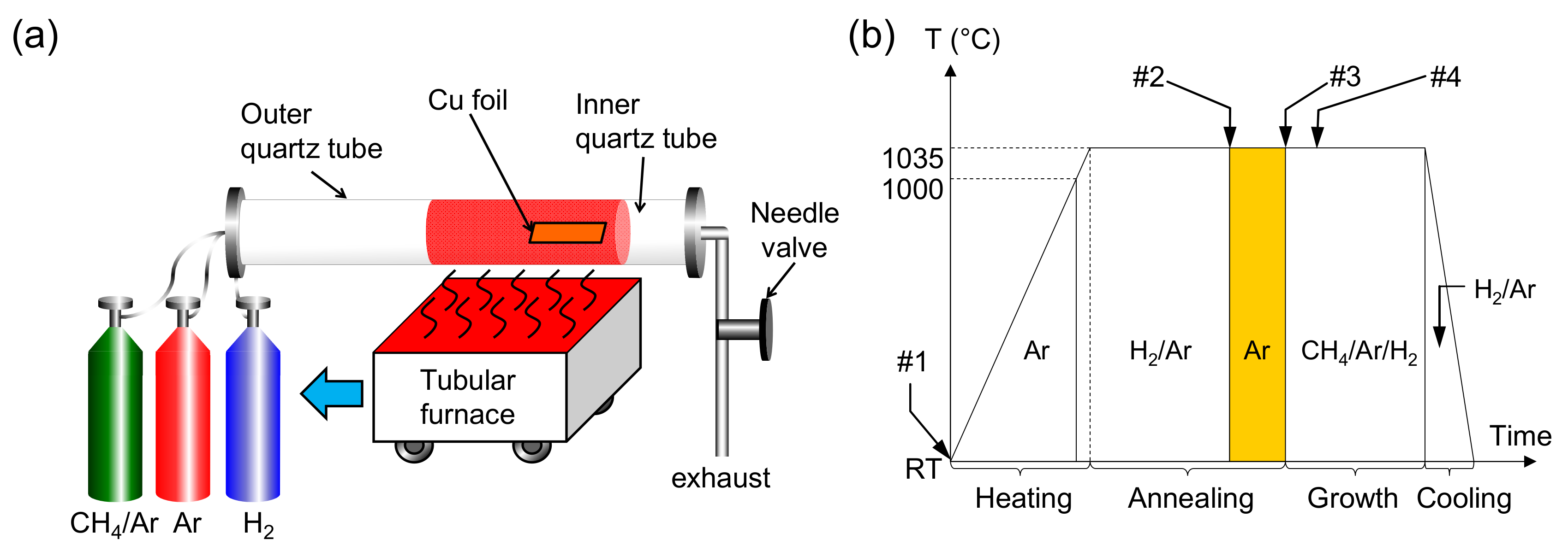
Figure 2.
Effect of Ar annealing on density of graphene domains. (a–c) Optical microscope images of CVD graphene on Cu with different Ar annealing time (0, 5, and 15 min), while H2 annealing time was fixed at 15 min; (d) CVD graphene grown after H2/Ar annealing for 45 min without Ar annealing; (e) Dependence of average density of graphene domains on Ar annealing time with two different flow rates for the growth. Square (black) and circle (red) plots correspond to the gas flows of 15/500 and 15/1000 sccm of H2/diluted CH4 in Ar (H2/CH4), respectively. Density of graphene domains is drastically decreased by Ar annealing for both growth conditions.
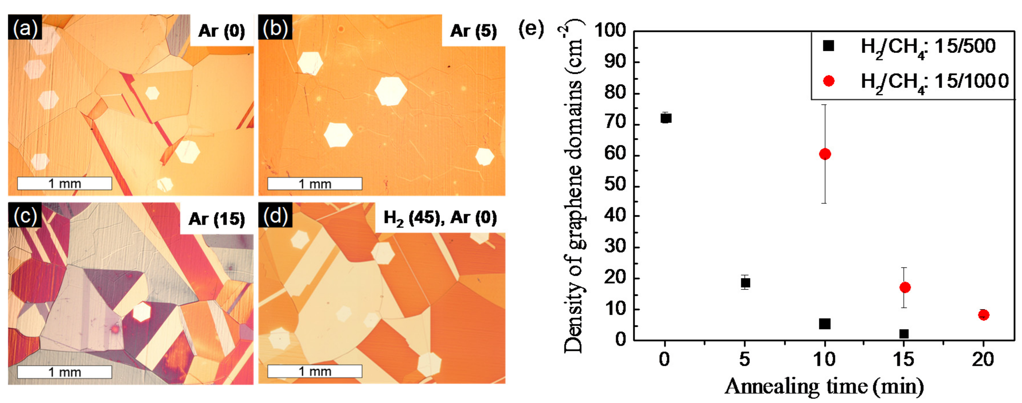
Figure 3.
XPS analysis of annealed Cu foils without growth of graphene. (a,b) High-resolution O1s and Cu2p3/2 XPS depth profiling of Cu foils with Ar annealing for 5 min; (c) Dependence of oxygen concentration on depth from surface of Cu foils with different Ar annealing time.
Figure 3.
XPS analysis of annealed Cu foils without growth of graphene. (a,b) High-resolution O1s and Cu2p3/2 XPS depth profiling of Cu foils with Ar annealing for 5 min; (c) Dependence of oxygen concentration on depth from surface of Cu foils with different Ar annealing time.

Figure 4.
Raman spectroscopy of Cu foils after intentional oxidization in air. (a) Raman spectra of the Oxi-foil (red line) and the Oxi-CVD (blue line). The Raman spectrum of the Oxi-CVD was taken at the Cu surface uncovered by grapheme; (b) High resolution Raman spectra around the peaks of 150 and 217 cm−1. Vertical broken lines and cursors are eye guides to compare Raman peaks.
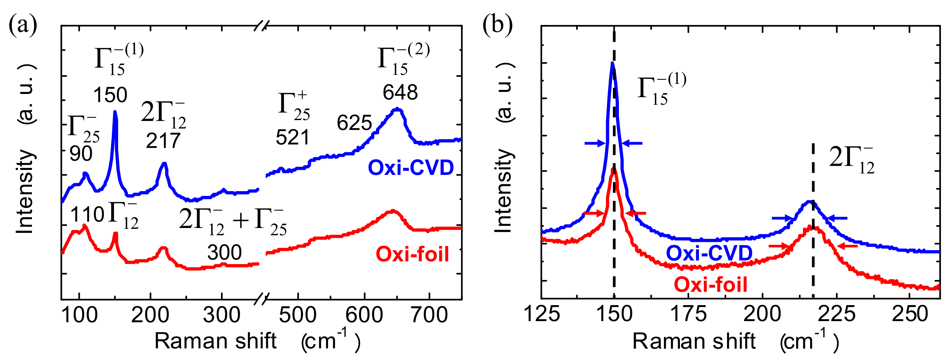
Figure 5.
(a) Evolution of an XPS depth profile of oxygen in Cu foil by CVD process. Cu foils of “raw Cu”, “H2: 15 min”, “Ox: 10 min”, and “Red: 5 min” were obtained after cooling down at #1–4 shown in Figure 1b, respectively; (b) Dependence of the average domain diameter of graphene grown with Ar annealing for 0 and 20 min on growth time.

Figure 6.
Effect of gas ambient on the heating and annealing process before Ar annealing on the morphology of Cu and the density of graphene. Low (a–c) and high magnification (d–f) optical microscope images of CVD graphene on Cu obtained by the Ar heating followed by H2/Ar (a,d); heating and annealing in H2/Ar (b,e); and heating and annealing in Ar (c,f).
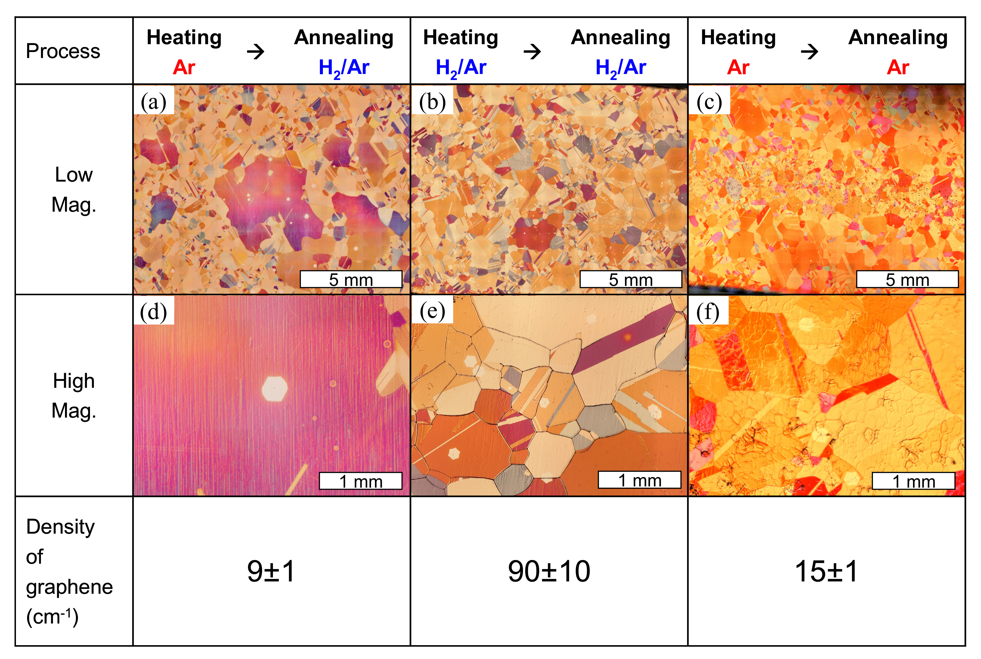
Figure 7.
(a) Optical microscope image of large-sized single-crystal graphene. The graphene was grown by a CVD with the H2/Ar and the Ar annealing for 100 and 35 min, respectively; (b) Raman spectrum of a millimeter scale CVD graphene transferred on a SiO2/Si substrate.
Figure 7.
(a) Optical microscope image of large-sized single-crystal graphene. The graphene was grown by a CVD with the H2/Ar and the Ar annealing for 100 and 35 min, respectively; (b) Raman spectrum of a millimeter scale CVD graphene transferred on a SiO2/Si substrate.

Figure 8.
Schematic illustration of the evolution of the Cu surface during the CVD. The initial, H2/Ar annealing, Ar annealing, and incubation time correspond to the CVD process at #1–4 in Figure 1b, respectively.
Figure 8.
Schematic illustration of the evolution of the Cu surface during the CVD. The initial, H2/Ar annealing, Ar annealing, and incubation time correspond to the CVD process at #1–4 in Figure 1b, respectively.

Table 1.
Comparison of Raman peaks in Figure 4b.
Table 1.
Comparison of Raman peaks in Figure 4b.
| Sample | 2Γ12 | |||
|---|---|---|---|---|
| Peak Position (cm−1) | FWHM (cm−1) | Peak Position (cm−1) | FWHM (cm−1) | |
| Oxi-CVD | 149.6 | 5.0 | 216.1 | 13.8 |
| Oxi-foil | 149.9 | 5.7 | 216.9 | 17.9 |
© 2017 by the authors. Licensee MDPI, Basel, Switzerland. This article is an open access article distributed under the terms and conditions of the Creative Commons Attribution (CC BY) license (http://creativecommons.org/licenses/by/4.0/).
Share and Cite
MDPI and ACS Style
Suzuki, S.; Terada, Y.; Yoshimura, M. Suppression of Graphene Nucleation by Turning Off Hydrogen Supply Just before Atmospheric Pressure Chemical Vapor Deposition Growth. Coatings 2017, 7, 206. https://doi.org/10.3390/coatings7110206
AMA Style
Suzuki S, Terada Y, Yoshimura M. Suppression of Graphene Nucleation by Turning Off Hydrogen Supply Just before Atmospheric Pressure Chemical Vapor Deposition Growth. Coatings. 2017; 7(11):206. https://doi.org/10.3390/coatings7110206
Chicago/Turabian StyleSuzuki, Seiya, Yoshifumi Terada, and Masamichi Yoshimura. 2017. "Suppression of Graphene Nucleation by Turning Off Hydrogen Supply Just before Atmospheric Pressure Chemical Vapor Deposition Growth" Coatings 7, no. 11: 206. https://doi.org/10.3390/coatings7110206
Note that from the first issue of 2016, this journal uses article numbers instead of page numbers. See further details here.