
In-Situ Growth and Characterization of Indium Tin Oxide Nanocrystal Rods


1
School of Material Science and Engineering, Qilu University of Technology, Jinan 250353, China
2
State Key Laboratory of Crystal Materials, Shandong University, Jinan 250100, China
*
Authors to whom correspondence should be addressed.
Coatings 2017, 7(12), 212; https://doi.org/10.3390/coatings7120212
Submission received: 31 October 2017
/
Revised: 16 November 2017
/
Accepted: 22 November 2017
/
Published: 25 November 2017
(This article belongs to the Special Issue Functional Oxide and Oxynitride Coatings)
Abstract
:Indium tin oxide (ITO) nanocrystal rods were synthesized in-situ by a vapor-liquid-solid (VLS) method and electron beam evaporation technique. When the electron-beam gun bombarded indium oxide (In2O3) and tin oxide (SnO2) mixed sources, indium and tin droplets appeared and acted as catalysts. The nanocrystal rods were in-situ grown on the basis of the metal catalyst point. The nanorods have a single crystal structure. Its structure was confirmed by X-ray diffraction (XRD) and transmission electron microscopy (TEM). The surface morphology was analyzed by scanning electron microscopy (SEM). During the evaporation, a chemical process was happened and an In2O3 and SnO2 solid solution was formed. The percentage of doped tin oxide was calculated by Vegard’s law to be 3.18%, which was in agreement with the mixture ratio of the experimental data. The single crystal rod had good semiconductor switch property and its threshold voltage of single rod was approximately 2.5 V which can be used as a micro switch device. The transmission rate of crystalline nanorods ITO film was over 90% in visible band and it was up to 95% in the blue green band as a result of the oxygen vacancy recombination luminescence.
1. Introduction
Indium tin oxide (ITO) is a metallic oxide material with good conductivity [1], high transparency [2] and optical nonlinearity [1,2,3]; As a conductive material, ITO film was widely used in [4] semiconductor devices [5,6,7], for example liquid crystal displays, solar cells and light emitting diodes [5] etc. Nanostructured ITO [8] has many new applications because of its unique surface [9] and quantum effects [10]. Nanometer-scale structured ITO material has a high specific surface area and can be applied in cells [11] and gas sensors [12,13]; it has also demonstrated gas sensitivity in the field of environmental sensitive exploration [14,15]. Although many other transparent conducting oxide thin-films have been developed to replace ITO film [16,17], ITO films are still the most widely used in commercial applications. As a commercially available film, the ITO research focus is on application fields or its preparation techniques. For example, ITO nanorods have been synthesized by radio frequency magnetron sputtering deposition [18], sol electrophoresis [19] and its characteristic was studied accordingly. Hamid [20] have analyzed the effect of substrate temperature on the electrical conductivity and transparency of ITO films. Canhola [21] studied the role of annealing environment on the performances of large area ITO films. The performance was improved GaSb-based solar cells with ITO nanorod array [22]. The concepts of ITO nanoantenna arrays [23] have been proposed. ITO confronted with the bottleneck in applications of photon conduction and flexible displays [24] for its brittle and polycrystalline natures.
In this work, ITO single-crystalline nanorods were fabricated at a substrate temperature of 300 °C by an electron beam evaporation technique (FU-20TEB-ITO, Fulinten Engineering Co. Ltd., Taiwan). A large area of uniform nanocrystal rod film can be proposed by using electron beam evaporation technique without other special equipment or additional functions. Compared to the existing ITO nanostructures [18,20], the ITO nanorods of we prepared have a single crystal structure and theirs length can be controlled simply by growth time. In-depth discussions and analyses have been carried out on the ITO nanostructured films.
The formation mechanism of the single-crystalline nanorods was based on a vapor-liquid-solid (VLS) model. When the electron-beam gun bombarded indium oxide and tin oxide mixed sources, indium and tin droplets appeared and acted as crystal growth auto-catalysts. The nanocrystal rods were in-situ grown from the metal catalyst points. Its crystalline structure was confirmed to a cubic from X-ray diffraction (XRD) and transmission electron microscopy (TEM) results. Indium (In) and tin (Sn) oxide solid solutions have undergone a chemical change and were formed during the VLS process. The percentage of doped tin oxide was calculated by Vegard’s law to be 3.18%, which was responsible for the shift in the XRD peaks and corresponded to the change in lattice parameter. The properties of the crystalline ITO nanorods were measured by conductivity measurement system with SEM image acquisition (ZEISS SUPRA55, Carl Zeiss AG, Oberkochen, Germany) and ultraviolet visible spectrophotometer (EMCLAB EMC-61PC-UV, Duisburg, Germany). The deep mechanism of light transmittance distribution was discussed.
2. Experimental
Optical glass substrates were placed in the electron-beam evaporation apparatus after being cleaned. The evaporation source was a homogenously mixed 95% In2O3 and 5% SnO2. A 1 μm thick oxide layer was deposited on the glass substrates after the substrate temperature reached the set point of 300 °C in the FU-20TEB-ITO equipment. The Voltage and power were 200 V and 5000 W of the evaporation equipment. Its pressure was set 1 × 10⁻⁴ mTorr in the chamber. The distance was 60 cm between the source and sample. The growth rate was kept constant at 1 Å/s.
Scanning-electron microscopy (SEM Hitachi S-4800, Hitachi Group, Tokyo, Japan), X-ray diffraction (XRD Bruker D-8 X Advance, Bruker Corporation, Karlsruhe, Germany) and transmission electron microscopy (TEM JEOL JEM-2100F, JEOL, Tokyo, Japan) were employed to characterize the crystallinity and detailed structure of the obtained nano-crystalline ITO.
The X-ray source was Cu (Kα = 0.1542 nm). The scanning step width was 0.08°, and the scan range was from 10° to 90°. The semiconductor switch property was measured by conductivity measurement system with SEM image acquisition (ZEISS SUPRA55). During the current-voltage test, first, the single crystalline nanorod was observed by SEM equipment, then the test probe was close to the single crystal rod and gradually applied current-voltage test. The optical transmittance characteristic of crystalline ITO nanorods film was analyzed by ultraviolet visible spectrophotometer (EMCLAB EMC-61PC-UV).
3. Results and Analysis
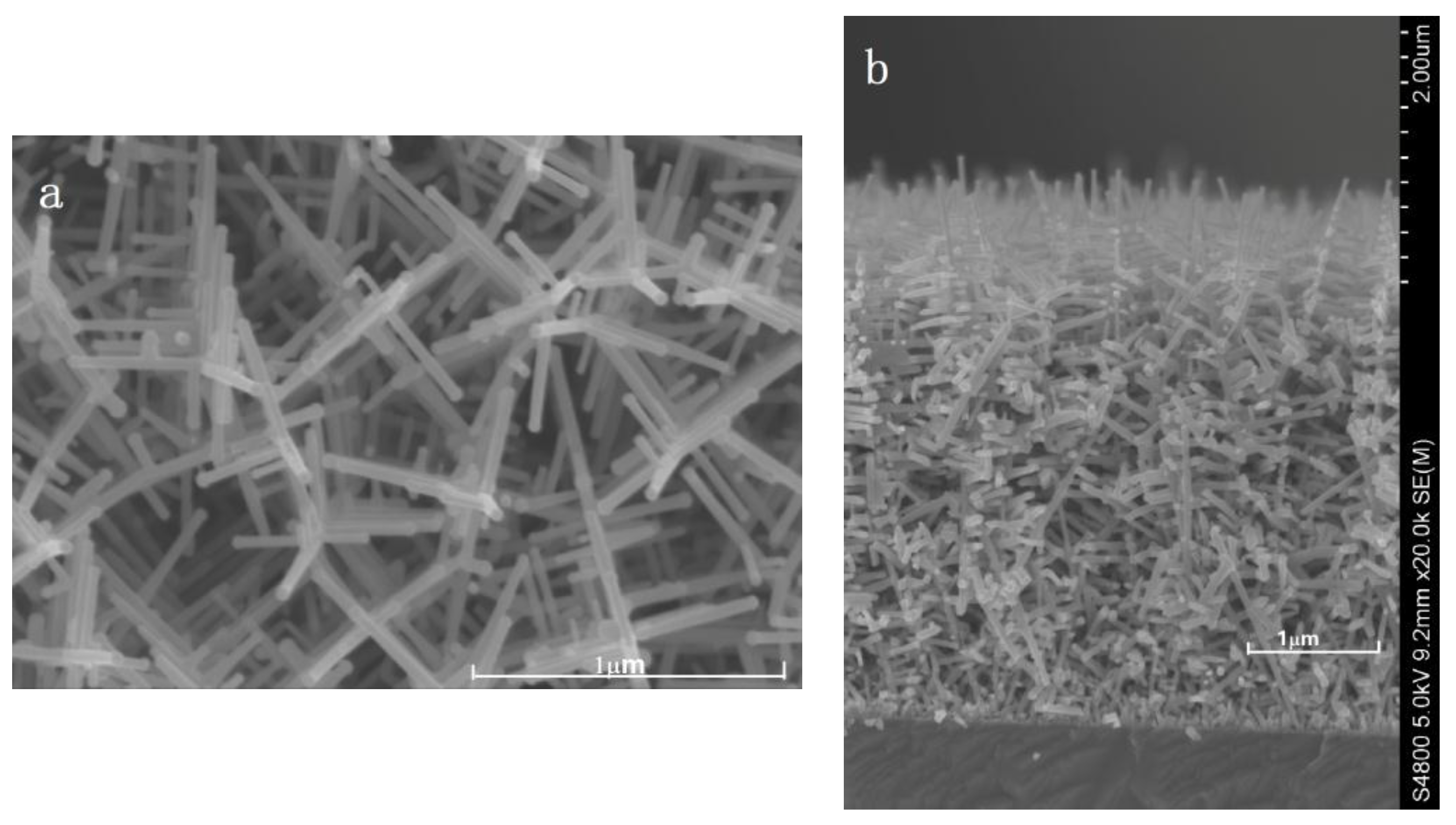
Figure 1 shows SEM images of the ITO films obtained at substrate temperatures of 300 °C. Randomly disordered nano-sized ITO rods with good quality single crystals were obtained.
The ITO nanometer crystals were formed by the VLS mechanism, yielding single-crystal morphology with a cap. The VLS theory was first proposed by Wagner and Ellis in 1964 [25]. In the VLS mechanism, the catalyst forms a liquid alloy at the eutectic temperature and then target material diffuses into the liquid alloy droplet. After reaching the solubility limit at the liquid-solid interface, crystal nucleus precipitates inducing nanocrystal growth. The nucleation with respect to the thermodynamics of adsorption and the kinetics of crystal growth has been given proposed and studied [26,27].
In our experiments, the evaporated ITO source (In2O3 95%-SnO2 5%) decomposed into In and Sn metal vapors under the high voltage electron-beam bombardment. The metal vapor condensed into liquid droplets on the surface of the glass substrate at 300 °C. The liquid metal droplets acted as a metal catalyst and absorbed oxide vapor, which diffused into the droplets. Nanometer sized crystal nuclei formed when the oxide in the droplet reached saturation. As the liquid nuclei constantly absorbed the source vapor and reached super-saturation, ITO crystals were formed and began to grow in-situ.
As shown in Figure 1, the ITO nanocrystal rods exhibited disordered random orientation, and the size of the droplets at the tips of the dendrites did not exceed 50 nm. The dendrites were in the range of 40–50 nm in diameter.
Figure 2 shows X-ray diffraction patterns of the cubic structure In2O3 and ITO crystalline rods grown at substrate temperatures of 300 °C. The ITO nanocrystal rods were found to have the centered cubic structure of In2O3.
The diffraction peaks at 2θ = 30.580°, 35.466°, 51.037° and 60.676° were assigned to the (222), (400), (440) and (622) reflections of cubic In2O3. Compared with that of the In2O3 cubic crystal, the XRD spectra of the ITO nanocrystal rods displayed all the same peaks but shifted slightly to higher 2θ. This peak shift can be explained by the In2O3 crystal changing to tin-doped In2O3 during the evaporation process, although its crystal structure remaining cubic [28,29].
From the XRD pattern of the ITO nanocrystal rods, the strongest peak was at 2θ = 36.142°, corresponding to the (400) reflection. According to the Bragg diffraction Formula (1),
Using the values, θ = 18.071° radian, λ = 1.542 Å, and n = 4, the parameter d was calculated to be 9.947 Å, which is quite similar to the lattice parameter of ITO nanocrystal rods. An In2O3 and SnO2 substitutional solid solution was formed. The ITO nanocrystal could thus be considered SnO2 doped In2O3, as SnO2 has a tetragonal crystal structure.
The relationship between mixed element composition and the lattice constants satisfies Vegard’s law, the first approximate Formula (2),
The lattice parameters of In2O3 and SnO2 respectively were 10.118 Å and 4.738 Å by a look-up PDF cards (PDF#06-0416 and PDF#41-1445). The parameter for ITO was 9.947 Å in the above calculation.
These values were used with Formula (2) to obtain x = 96.82%. The percentage of SnO2 doped in In2O3 was 3.18%, which confirmed the mixture ratio of oxide materials. The recrystallization process during the evaporation was a chemical one. In2O3 and SnO2 were broken down by evaporation and generated an indium tin oxide substitutional solid solution again. Sn atom replaced In atom into the crystal lattice and form alloy.
The ITO also had a cubic crystal structure. Because the ionic radius of Sn4+ is smaller than the radius of In3+ in the cubic lattice, the lattice constant of ITO was smaller than that of In2O3, which shifted the diffraction peaks to higher 2θ, as shown in Figure 2.
The strongest peak of the ITO crystal corresponded to the (400) reflection. The other peaks were very weak and nearly disappeared. This indicated that the ITO nanocrystal rods were [001] oriented and that the (100) crystal plane was the major exposed facet.
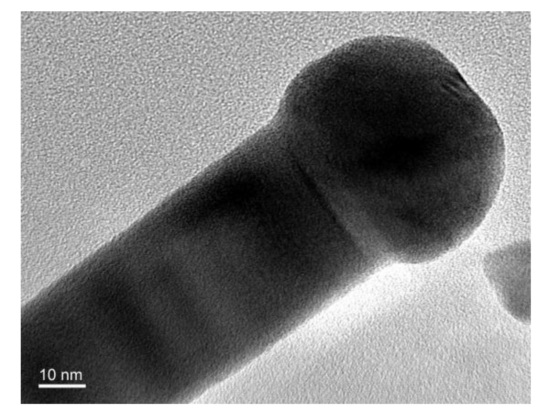
Figure 3 shows a TEM image of the single nanocrystal ITO, which provides an insight into the structure of the crystallized ITO. The diameter of the nanocrystal branch was approximately 50 nm. Metal droplets existed on the top of every branch, with diameters of approximately 50 nm. This result is in agreement with the crystal growth VLS model.
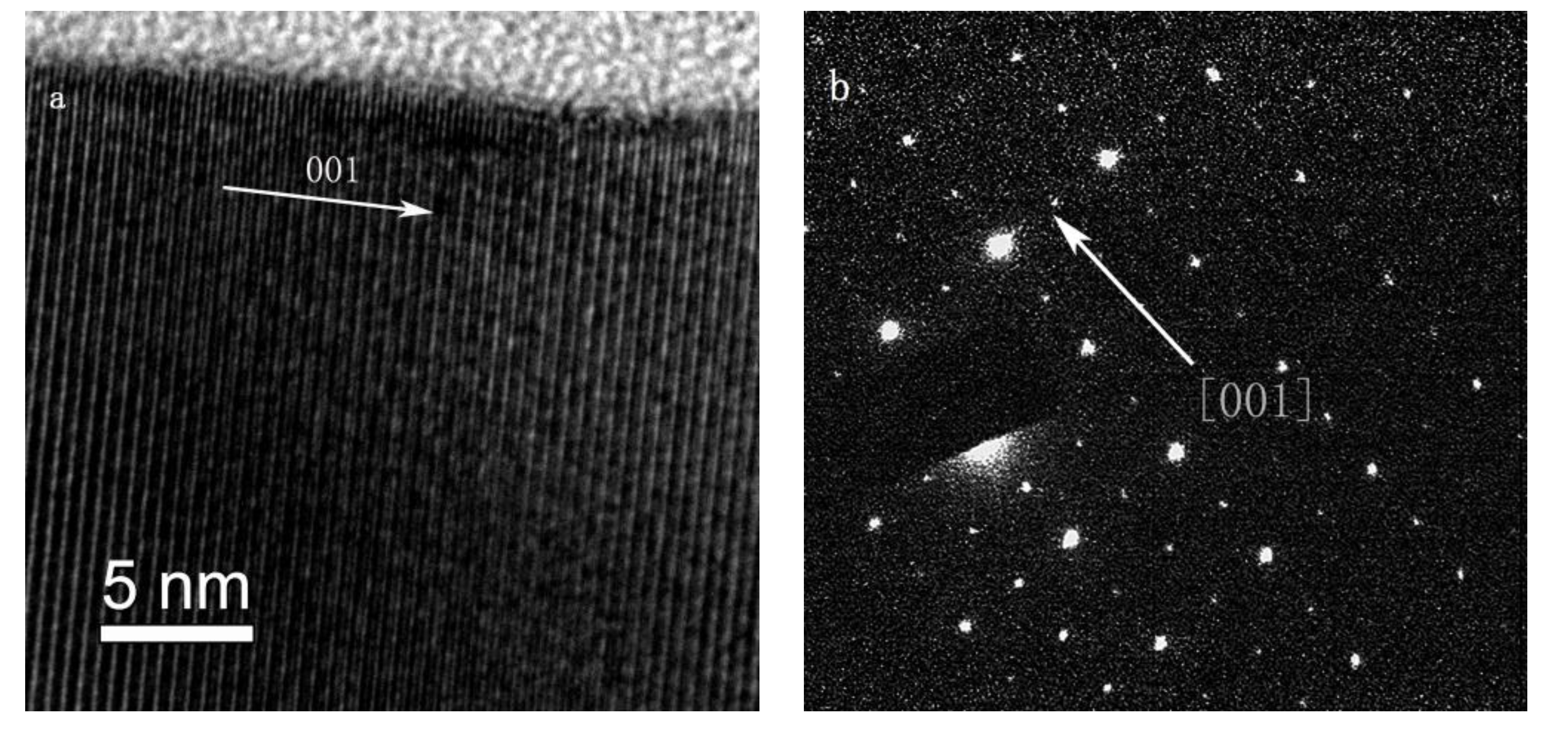
The high resolution transmission electron microscopy (HRTEM) image shown in Figure 4a reveals that the ITO nanocrystal rods had a body centered cubic single crystal structure. The crystal lattice was very complete and continuous, and was clearly identifiable as a cubic ITO phase with (001) and (010) inter-planar spacing. This indicated that the growth direction was <100>. The associated selected-area electron diffraction pattern of the imaged ITO shows clear dots corresponding to the (100) planes in Figure 4b, which confirms that the ITO rods were cubic crystals.
Figure 5 shows the current-voltage characteristic of the ITO single crystal rod in the voltage range of 0–5.0 V. C-1 and C-2 are any two samples of ITO nanorod in random selection. Consistent semiconductor pn junction features are all shown in the random two single crystal rods in Figure 5. The ITO nanocrystal rod exhibited good semiconductor properties and its threshold voltage was approximately 2.5 V.
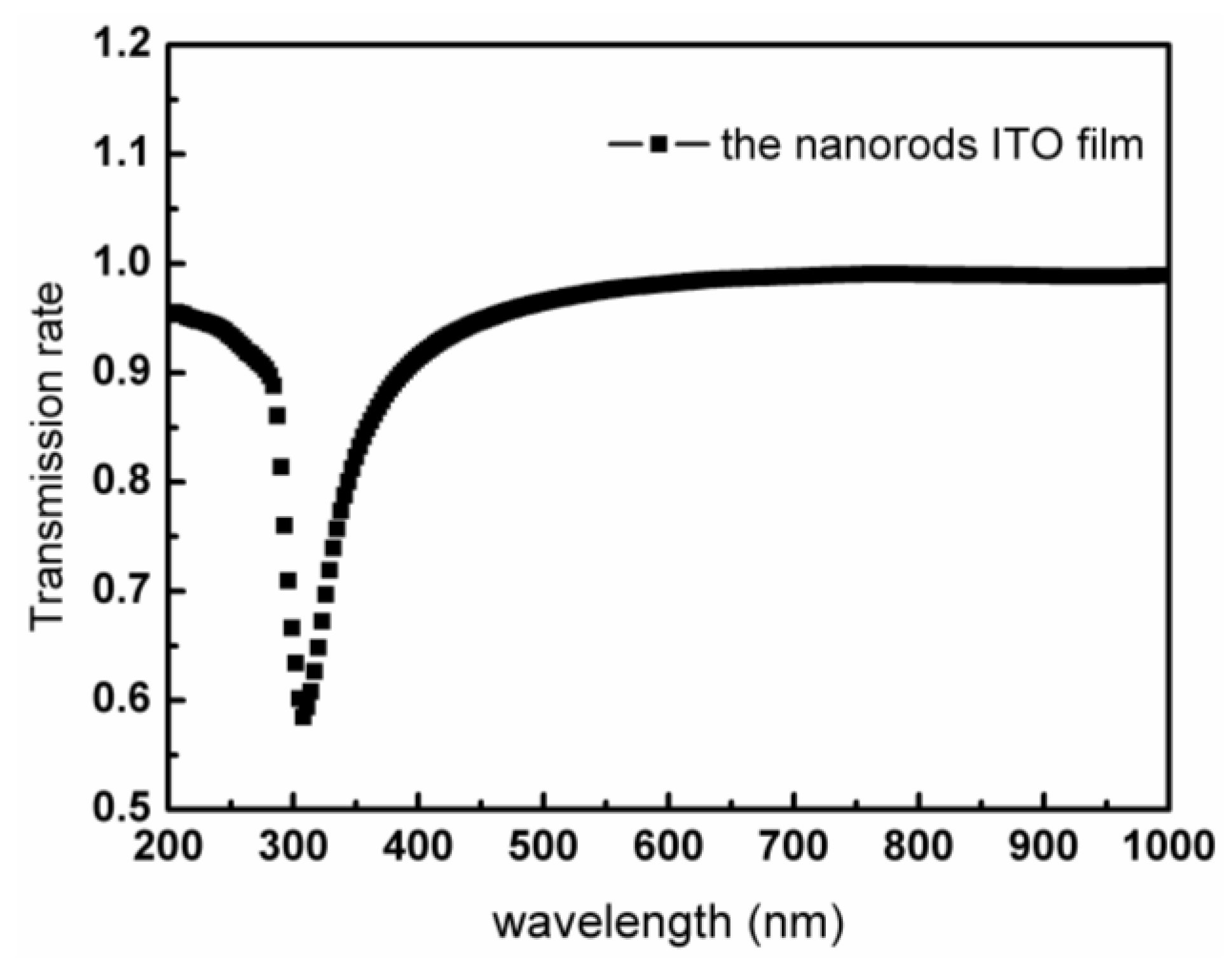
Figure 6 is the transmission rate curve of the crystalline ITO nanorods film in the wavelength range of 300–1000 nm. From the transmission rate curve, the transmittance of crystalline ITO film is over 90% in the visible, and that is up to 95% in the blue green band. For many oxygen vacancies exist in the cubic structure of ITO nanocrystals. The cavity excited by photons and the electron that occupied the oxygen vacancy recombined luminescence to enhance the transmission rate of this band. Strong absorption occurs near the wavelength of 300 nm because its high crystallinity leads to weak quantum-confinement-effect [30].
4. Conclusions
In summary, ITO nanocrystal rods were grown by the VLS growth method during the process of electron-beam evaporation. The growth mechanism of the ITO nanocrystal rods was auto-catalytic in-situ growth via the VLS process. The ITO nanorods exhibited a perfect crystalline cubic phase structure. XRD and TEM results revealed that the crystallization was [001] oriented and the presented facet was the (100) crystal planes. A binary (In2O3 and SnO2) solid solution was formed during the evaporation process. The percentage of doped tin oxide was calculated by the first approximate Vegard’s law to be 3.18%, which was in agreement with the mixture ratio of the experimental source. The ITO single nanocrystal rod exhibited good semiconductor switch property and its threshold voltage was approximately 2.5 V. The transmittance of ITO nanorods film was over 90% in visible light band, which was due to the oxygen vacancy recombination luminescence in some specific bands. Strong absorption in the wavelength of 300 nm was from weak quantum-confinement-effect of its high crystallinity.
Acknowledgements
This work was supported by Shandong Focus on R&D Projects grant No. 2016GGX102040. The author wishes to express the grateful to Shaozhi Deng team of Sun Yat-sen University for providing the IV test.
Author Contributions
The entire study was completed by Yan Shen with the assistance of Youxin Lou, Zhihao Wang and Xiangang Xu. The notes as follows: Yan Shen and Xiangang Xu designed and planned the research topic; Yan Shen conceived and carried out the experiments, measured and analyzed the date, wrote the paper; Lou and Wang performed the experiments.
Conflicts of Interest
The authors declare no conflict of interest.
References
- Lin, Y.C.; Chang, S.J.; Su, Y.K.; Tsai, T.Y.; Chang, C.S.; Shei, S.C.; Hsu, S.J.; Liu, C.H.; Liaw, U.H.; Chen, S.C.; et al. Nitride-based light-emitting diodes with Ni/ITO p-type ohmic contacts. IEEE Photonics Technol. Lett. 2002, 14, 1668–1670. [Google Scholar] [CrossRef]
- Phillips, J.M.; Cava, R.J.; Thomas, G.A.; Carter, S.A.; Kwo, J.; Siegrist, T.; Krajewski, J.J.; Marshall, J.H.; Peck, W.F., Jr.; Rapkine, D.H. Zinc-indium-oxide: A high conductivity transparent conducting oxide. Appl. Phys. Lett. 1995, 67, 2246–2248. [Google Scholar] [CrossRef]
- Alam, M.Z.; De Leon, I.; Boyd, R.W. Large optical nonlinearity of indium tin oxide in its epsilon-near-zero region. Science 2016, 352, 795–797. [Google Scholar] [CrossRef] [PubMed]
- Shen, Y.; Xu, X.; Liu, Q.; Zuo, Z.; Liu, H.; Zhang, M.; Hu, X. Effects of indium–tin oxide film morphologies on light-output characteristics of GaN-based light-emitting diodes. J. Nanoelectron. Optoelectron. 2014, 9, 549–553. [Google Scholar] [CrossRef]
- Jin, S.X.; Li, J.; Lin, J.Y.; Jiang, H.X. InGaN/GaN quantum well interconnected microdisk light emitting diodes. Appl. Phys. Lett. 2000, 77, 3236–3238. [Google Scholar] [CrossRef]
- Das, S.R.; Sadeque, S.; Jeong, C.; Chen, R.; Alam, M.A.; Janes, D.B. Copercolating networks: An approach for realizing high-performance transparent conductors using multicomponent nanostructured networks. Nanophotonics 2016, 5, 180–195. [Google Scholar] [CrossRef]
- Chiu, C.J.; Shih, S.S.; Weng, W.Y.; Chang, S.J.; Hung, Z.D.; Tsai, T.Y. Deep UV Ta2O5/zinc-indium-tin-oxide thin film photo-transistor. IEEE Photonics Technol. Lett. 2012, 24, 1018–1020. [Google Scholar] [CrossRef]
- Kim, J.W.; Jeon, H.J.; Lee, C.L.; Ahn, C.W. Fabrication of three-dimensional hybrid nanostructure-embedded ITO and its application as a transparent electrode for high-efficiency solution processable organic photovoltaic devices. Nanoscale 2017, 9, 3033–3039. [Google Scholar] [CrossRef] [PubMed]
- Nuchuay, P.; Chaikeeree, T.; Horprathum, M.; Mungkung, N.; Kasayapanand, N.; Oros, C.; Limwichean, S.; Nuntawong, N.; Chananonnawathorn, C.; Patthanasettakul, V.; et al. Engineered omnidirectional antireflection ITO nanorod films with super hydrophobic surface via glancing-angle ion-assisted electron-beam evaporation deposition. Curr. Appl. Phys. 2017, 17, 222–229. [Google Scholar] [CrossRef]
- Pattathil, P.; Giannuzzi, R.; Qualtieri, A.; Barawi, M.; Manca, M. Widely tunable localized surface plasmon scattering in mesoporous ITO electrodes. MRS Adv. 2016, 1, 3903–3908. [Google Scholar] [CrossRef]
- Richardson, B.J.; Zhu, L.; Yu, Q. Design and development of plasmonic nanostructured electrodes for ITO-free organic photovoltaic cells on rigid and highly flexible substrates. Nanotechnology 2017, 28, 165401. [Google Scholar] [CrossRef] [PubMed]
- Guo, X.M.; Zhao, J.T.; Yin, X.T.; Huang, S.L. Sensitivity and selectivity of SnO2-based sensor for CO and H2 detections: A novel method to detect simultaneously the CO and H2 concentrations. Adv. Sci. Technol. 2017, 99, 40–47. [Google Scholar] [CrossRef]
- Yoon, J.-W.; Kim, J.-S.; Kim, T.-H.; Hong, Y.J.; Kang, Y.C.; Lee, J.-H. A new strategy for humidity independent oxide chemiresistors: Dynamic self-refreshing of In2O3 sensing surface assisted by layer-by-layer coated CeO2 nanoclusters. Small 2016, 12, 4229–4240. [Google Scholar] [CrossRef] [PubMed]
- Zhang, J.; Hu, J.; Zhu, Z.Q.; Gong, H.; O’Shea, S.J. Quartz crystal microbalance coated with sol–gel-derived indium–tin oxide thin films as gas sensor for NO detection. Colloids Surf. A Physicochem. Eng. Aspects 2004, 236, 23–30. [Google Scholar] [CrossRef]
- Liu, P.T.; Chou, Y.T.; Teng, L.F. Environment-dependent metastability of passivation-free indium zinc oxide thin film transistor after gate bias stress. Appl. Phys. Lett. 2009, 95, 233504. [Google Scholar] [CrossRef]
- Minami, T. Present status of transparent conducting oxide thin-film development for Indium-Tin-Oxide (ITO) substitutes. Thin Solid Films 2008, 516, 5822–5828. [Google Scholar] [CrossRef]
- Lyubchyk, A.; Vicente, A.; Soule, B.; Alves, P.U.; Mateus, T.; Mendes, M.J.; Águas, H.; Fortunato, E.; Martins, R. Mapping the electrical properties of ZnO-based transparent conductive oxides grown at room temperature and improved by controlled postdeposition annealing. Adv. Electron. Mater. 2016, 2. [Google Scholar] [CrossRef]
- Park, J.H.; Park, H.K.; Jeong, J.; Kim, W.; Min, B.K.; Do, Y.R. Wafer-scale growth of ITO nanorods by radio frequency magnetron sputtering deposition. J. Electrochem. Soc. 2011, 158, K131–K135. [Google Scholar] [CrossRef]
- Limmer, S.J.; Cruz, S.V.; Cao, G.Z. Films and nanorods of transparent conducting oxide ITO by a citric acid sol route. Appl. Phys. A 2004, 79, 421–424. [Google Scholar] [CrossRef]
- Fallah, H.R.; Vahid, M.J. Substrate temperature effect on transparent heat reflecting nanocrystalline ITO films prepared by electron beam evaporation. Renew. Energy 2010, 35, 1527–1530. [Google Scholar] [CrossRef]
- Canhola, P.; Martins, N.; Raniero, L.; Pereira, S.; Fortunato, E.; Ferreira, I.; Martins, R. Role of annealing environment on the performances of large area ITO films produced by RF magnetron sputtering. Thin Solid Films 2005, 487, 271–276. [Google Scholar] [CrossRef]
- Lee, H.Y.; Huang, H.L.; Pchelyakov, O.P.; Pakhanov, N.A. Performance improvement mechanisms of bias-assisted photoelectrochemical treated GaSb-based solar cells with ITO nanorod array. Prog. Photovolt. Res. Appl. 2016, 24, 195–199. [Google Scholar] [CrossRef]
- Chen, K.; Guo, P.; Dao, T.D.; Li, S.Q.; Ishiii, S.; Nagao, T.; Chang, R.P.H. Protein-functionalized indium-tin oxide nanoantenna arrays for selective infrared biosensing. Adv. Opt. Mater. 2017, 1700091. [Google Scholar] [CrossRef]
- He, L.; Tjong, S.C. Nanostructured transparent conductive films: Fabrication, characterization and applications. Mater. Sci. Eng. R Rep. 2016, 109, 1–101. [Google Scholar] [CrossRef]
- Wagner, R.S.; Ellis, W.C. Vapor-liquid-solid mechanism of single crystal growth. Appl. Phys. Lett. 1964, 4, 89–90. [Google Scholar] [CrossRef]
- Wagner, R.S.; Levitt, A.P. Whisker Technology; AP Levitt Wiley: New York, NY, USA, 1970; pp. 47–119. [Google Scholar]
- Venables, J.A.; Spiller, G.D.T.; Hanbucken, M. Nucleation and growth of thin films. Rep. Prog. Phys. 1984, 47, 399. [Google Scholar] [CrossRef]
- Detchprohm, T.; Hiramatsu, K.; Itoh, K.; Akasaki, I. Relaxation process of the thermal strain in the GaN/α-Al2O3 heterostructure and determination of the intrinsic lattice constants of GaN free from the strain. Jpn. J. Appl. Phys. 1992, 31, L1454. [Google Scholar] [CrossRef]
- Bel Hadj Tahar, R.; Ban, T.; Ohya, Y.; Takahashi, Y. Tin doped indium oxide thin films: Electrical properties. J. Appl. Phys. 1998, 83, 2631–2645. [Google Scholar] [CrossRef]
- Liu, Q.; Lu, W.; Ma, A.; Tang, J.; Lin, J.; Fang, J. Study of quasi-monodisperse In2O3 nanocrystals: Synthesis and optical determination. J. Am. Chem. Soc. 2005, 127, 5276–5277. [Google Scholar] [CrossRef] [PubMed]
Figure 1.
SEM micrographs of ITO films fabricated at a substrate temperature of 300 °C: (a) top view; (b) profile.
Figure 1.
SEM micrographs of ITO films fabricated at a substrate temperature of 300 °C: (a) top view; (b) profile.

Figure 2.
XRD patterns of In2O3 cubic crystal and ITO single-crystalline rods grown at 300 °C.
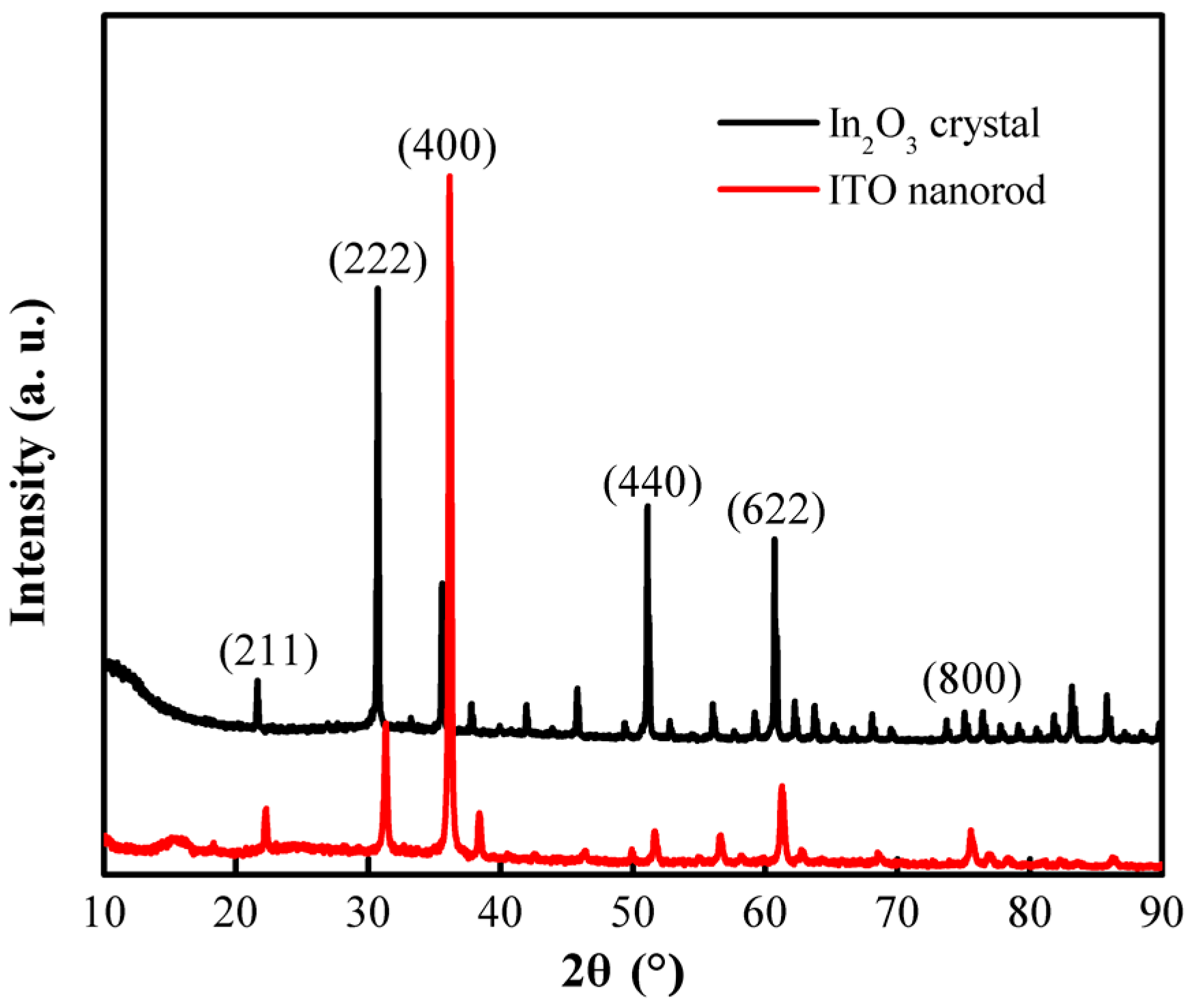
Figure 3.
TEM micrograph of a single ITO crystal rod.

Figure 4.
(a) HRTEM image of a typical single ITO crystal area; (b) an associated selected-area electron diffraction pattern.
Figure 4.
(a) HRTEM image of a typical single ITO crystal area; (b) an associated selected-area electron diffraction pattern.

Figure 5.
Current-voltage curves of a single ITO crystal rod from 0 to 5.0 V. (C-1 and C-2 are the any two nanorods of ITO).
Figure 5.
Current-voltage curves of a single ITO crystal rod from 0 to 5.0 V. (C-1 and C-2 are the any two nanorods of ITO).
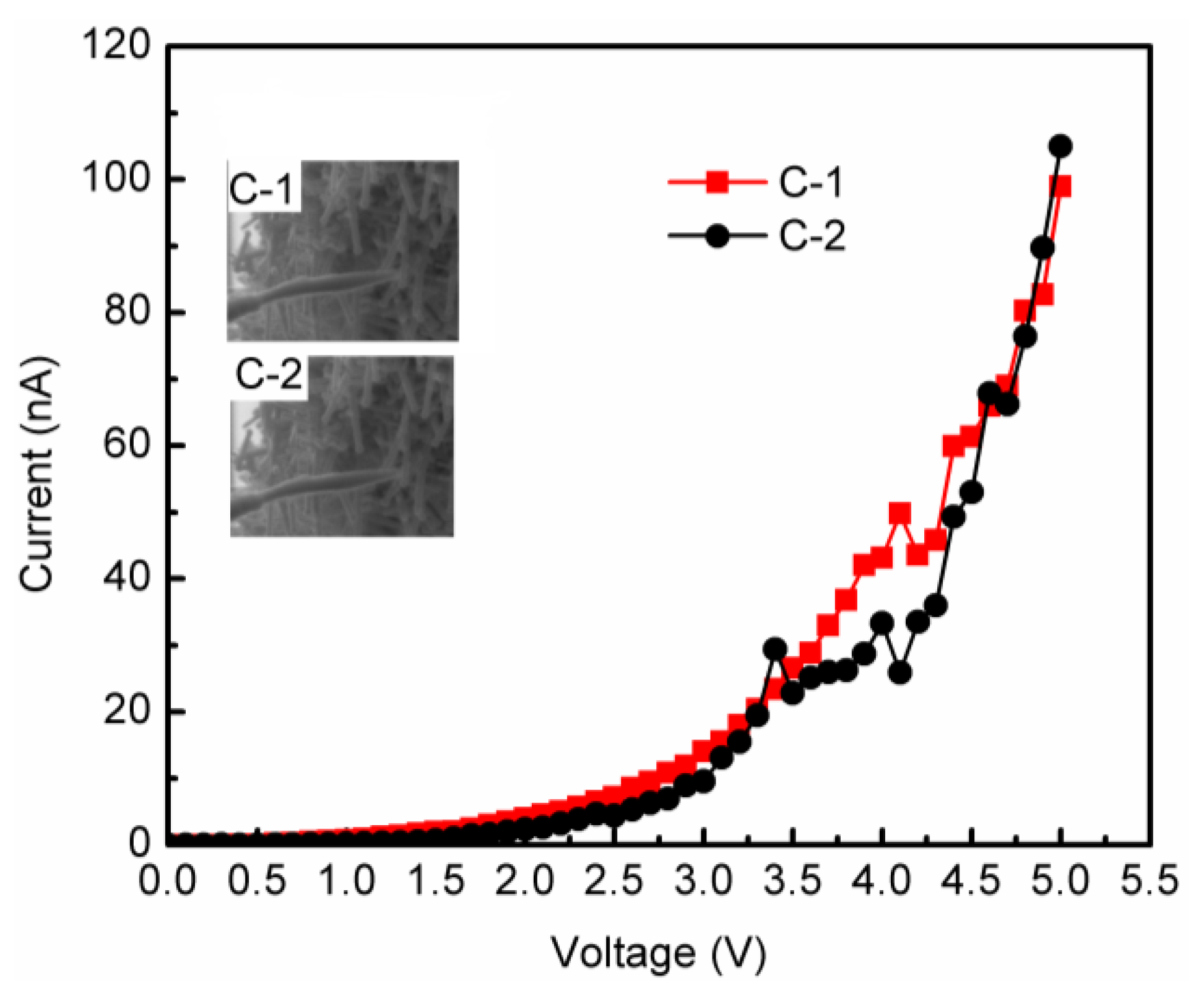
Figure 6.
Transmission rate of the crystalline ITO nanorods film in the wavelength range of 200–1000 nm.
Figure 6.
Transmission rate of the crystalline ITO nanorods film in the wavelength range of 200–1000 nm.

© 2017 by the authors. Licensee MDPI, Basel, Switzerland. This article is an open access article distributed under the terms and conditions of the Creative Commons Attribution (CC BY) license (http://creativecommons.org/licenses/by/4.0/).
Share and Cite
MDPI and ACS Style
Shen, Y.; Lou, Y.; Wang, Z.; Xu, X. In-Situ Growth and Characterization of Indium Tin Oxide Nanocrystal Rods. Coatings 2017, 7, 212. https://doi.org/10.3390/coatings7120212
AMA Style
Shen Y, Lou Y, Wang Z, Xu X. In-Situ Growth and Characterization of Indium Tin Oxide Nanocrystal Rods. Coatings. 2017; 7(12):212. https://doi.org/10.3390/coatings7120212
Chicago/Turabian StyleShen, Yan, Youxin Lou, Zhihao Wang, and Xiangang Xu. 2017. "In-Situ Growth and Characterization of Indium Tin Oxide Nanocrystal Rods" Coatings 7, no. 12: 212. https://doi.org/10.3390/coatings7120212
Note that from the first issue of 2016, this journal uses article numbers instead of page numbers. See further details here.