Article

Inkjet-Printed Chemical Solution Y2O3 Layers for Planarization of Technical Substrates

1
Oxolutia S.L, Avda. Castell de Barberà 26, Tallers 13, Nau 1, 08210 Barberà del Vallès, Spain
2
Departament de Física, Universitat Autònoma de Barcelona, 08193 Bellaterra, Spain
3
Institució Catalana de Recerca i Estudis Avançats (ICREA), Passeig Lluís Companys 23, 08010 Barcelona, Spain
4
KAO-Chimigraf, Carcassí, 6-8, Polígon Ind. Can Jardí, 08191 Rubí, Spain
5
Bruker HTS GmbH, Roengenstr. 9, D-63755 Alzenau, Germany
6
Institut de Ciència de Materials de Barcelona (ICMAB-CSIC), Carrer dels Til·lers s/n, Campus de la Universitat Autònoma de Barcelona, 08193 Bellaterra, Spain
*
Author to whom correspondence should be addressed.
Coatings 2017, 7(12), 227; https://doi.org/10.3390/coatings7120227
Submission received: 2 October 2017 / Revised: 16 November 2017 / Accepted: 25 November 2017 / Published: 11 December 2017
(This article belongs to the Special Issue Mechanical Behavior of Coatings and Engineered Surfaces)

Abstract

:
The implementation of the Chemical Solution Deposition (CSD) methodology with the Drop on Demand (DoD) inkjet printing (IJP) technology has been successfully employed to develop a Solution Deposition Planarization (SDP) method. We have used nanocrystalline yttrium oxide (Y2O3) to decrease the roughness of technical metallic substrates by filling the surface imperfections and thus avoiding costly polishing steps. This alternative process represents an outstanding methodology to reduce the final cost of the second-generation coated conductors manufacturing. Two Y2O3 metalorganic precursor ink formulations were successfully developed and tested to obtain surfaces as smooth as possible with adequate mechanical properties to hold the internal stress developed during the growth of the subsequent layers. By using these inks as precursors for IJP and after a proper tuning of the rheological and wetting parameters, we firstly obtained centimeter length uniform 100 nm-thick SDP-Y2O3 films on unpolished stainless-steel substrate from Bruker HTS. The scalability of the roll to roll (R2R)-IJP process to 100 m is then demonstrated on metallic substrates as well. A complete characterization of the prepared SDP-Y2O3 inkjet-printed layers was carried out using optical microscopy, FIB-SEM (Focus Ion Beam coupled to Scanning Electron Microscopy), XRD (X-ray Diffraction), AFM (Atomic Force Microscopy), reflectometry and nanoindentation techniques. Then, the morphology, thickness, crystallinity and mechanical properties were evaluated, together with the surface roughness in order to assess the resulting layer planarity. The impact of planarity was additionally studied via growth of biaxially textured buffer layers as well as further functional layers. 1.1 µm-thick YSZ layers with in-plane textures better than the stainless steel (SS) polished reference were successfully deposited on top of 100 nm SDP-Y2O3 films yielding 50% of Ic in contrast to the standard SS reference.

Graphical Abstract

1. Introduction

In the last years, functional ceramic oxides have brought a huge amount of new insights and applications. To wholly boost such advanced and rapidly evolving fields, low cost and scalable technologies have to be contemplated [1]. Chemical Solution Deposition (CSD) [2,3,4,5] has been demonstrated to be a powerful low-cost alternative for producing functional oxide epitaxial devices and nanostructured systems.
Particularly, the implementation of CSD with the inkjet printing (IJP) methodology [6,7,8,9,10] enables to obtain epitaxial films in long lengths with controlled thickness by adjusting the drop volume, the ink concentration and the drop density (i.e., number of drops per unit area).
Since the discovery of high temperature superconductors (HTS) [11,12,13], a lot of work has been developed to prepare long length conductors for power applications with high superconducting performances at reduced manufacturing costs. The use of adequate efficient and scalable methodologies to grow the YBa2Cu3O7−x (YBCO)-HTS as epitaxial films on flexible metallic substrates following a multistack architecture, i.e., coated conductors (CC’s) [14,15], spread completely out new paths for fast progress towards reaching the goals previously mentioned. After several years of intense research, the big challenge in R&D-CC has been to define affordable techniques for CC production, including preparation and conditioning of technical metallic substrates, either with textured (IBAD) [16] or thermomechanically textured (RABIT) [17,18] substrates, effectively protected by cap layers and the subsequent growth of the epitaxial YBCO films with high thickness at low cost/performance ratio.
Yttrium stabilized zirconia (YSZ) by Alternating Beam Assisted Deposition (ABAD) [19], La1−xSrxMnO3 by Chemical Solution Deposition (CSD) [20], CeO2 by Pulsed Laser Deposition (PLD) [21,22] or CSD [23,24], LaMnO3 by sputtering [25], La2Zr2O7 by CSD [26], TiN by IBAD [27], MgO by Inclined Substrate Deposition (ISD) [28] or IBAD [29] are examples of effective buffer layers to transfer the specific texture to the YBCO superconducting layer. All these approaches require that the metal substrate has a very smooth surface in the range of few nm in order for the crystals above to be aligned within a few degrees misorientation.
Mechanical polishing or electropolishing methods [30,31,32,33] are common methodologies for eliminating defects from the surface of the raw substrates and planarize them. Both methodologies exhibit some practical limitations as the duration of the process and the production of toxic waste disposal. Some years ago, the Solution Deposition Planarization (SDP) technique [34] has emerged as an alternative method to smooth surfaces using inks to fill the substrate defects and irregularities. This SDP method will clearly assist in cost reduction of the overall industrial process.
In recent years, we have started to explore the feasibility to fulfil the planarization of technical substrates by chemical methods mixing the chemical solution deposition methodology (CSD) together with the inkjet printing technology (IJP). In this basis, yttrium oxide (Y2O3) precursor solutions were inkjet deposited and thermally treated to form nanocrystalline homogeneous Y2O3 films on commercial metallic substrates. Parameters like the root mean square rms roughness of these SDP-Y2O3 films, the homogeneity and the adhesion, are essential to define the final quality of the complex CC architecture.
Several industrial and research groups have reported successful results regarding the SDP methodology and more specifically, concerning SDP-Y2O3 layers. Yang et al. [25] obtained critical current densities (Jc) about 2.4 MA/cm2 (sf, 77 K) on Hastelloy/SDP-Y2O3/IBAD-MgO/epi-MgO /LaMnO3sputtering/YBCOMOCVD CC architecture. Martynova et al. [35] described an effective method for smoothing Hastelloy C-276 tapes from rms roughness 9 nm (in 5 × 5 µm2 areas) to 0.8 nm (5 × 5 µm2) using optimized solvent based Y2O3 precursor solutions. They also reported 20 m length of 2G-HTS wire with Ic about 300 A on Hastelloy C276 substrate on planarized dip coated Al2O3 wire tape [36].
Sheehan et al. [34] demonstrated 0.5 nm (5 × 5 µm2) rms roughness dip coated Y2O3-SDP films starting from unpolished metal tapes prior to ion-beam textured MgO growth.
However, other institutions have used alumina (Al2O3) as another smoothing candidate [36] to substitute the widely used Y2O3. Paranthaman et al. [30] stated Jc values at 77 K and self-field of about 3 MA/cm2 on short length spin-coated Al2O3MOD-MgOIBAD templates, encouraging their transference to long lengths.

2. Materials and Methods

2.1. Metal-Organic Precursor Inks

2.1.1. Materials

The starting materials: yttrium acetate (Y(CH3COO)3, Aldrich, 99.9%, Saint Louis, MO, USA), diethanolamine (DEA, NH(CH2CH2OH)2, Aldrich, >98%), propionic acid (CH3CH2COOH, Panreac, 99%, Castellar del Vallès, Spain), 1-butanol (CH3CH2CH2CH2OH, Aldrich, 99.8%).

2.1.2. Metal-Organic Precursor Ink Preparation

Different Y2O3 precursor solutions from 0.2 M to 0.4 M (in yttrium) were prepared by dissolving yttrium acetate in propionic acid (26% v/v) at 35 °C. The mix is stirred until the complete salt dissolution. Then, diethanolamine (DEA) is slowly added, at 35 °C as well, and stirred during 15 min. The solution at this point becomes transparent. The mix is cooled down to room temperature and the volume was brought to the final concentration with n-butanol. The last step is the filtration through a syringe filter, (PTFE membrane, with pore size of 0.2 μm). These precursor solutions remain stable for some weeks.

2.1.3. Metal-Organic Precursor Ink Characterization

Due to the extremely great importance of inks’ physicochemical properties in the inkjet printing method to determine crucial processes such as drop formation and drop spreading and wetting, the ink parameters were routinely evaluated after their preparation prior to deposition [6,37]. The studied properties in the case of SDP precursor inks were viscosity, surface tension, contact angle, density and metal concentration. This preliminary study permits the carrying out of a quality control of the inks, as well as the determination of whether the as-prepared inks are found to be jettable with our inkjet printheads.

Viscosity Measurement

The viscosity was measured using a HAAKE RheosStress RS600 (Thermo Electron, GmbH, Waltham, MA, USA) equipped with a low inertia torque motor at 25 °C and 2880 s−1 of shear rate γ ˙ .

Surface Tension and Contact Angle Measurements

The measurements of surface tension and contact angle were performed by the pendant drop and sessile methods, respectively, which are based on the determination of the shape of a pendant/sessile drop by the balance between surface/interfacial tensions and an external force, such as gravity. One technique is the ADSA (Axisymmetric Drop Shape Analysis) [38,39,40], which determines the liquid/fluid interfacial tensions from the shape of an axisymmetric menisci due to the gravitational force. This technique for the sessile and pendant drop measurements accomplishes the contact angle and surface tension determination by finding the best fitting of the theoretical drop profile to the real one [41].
Along this work, contact angle and surface tension of the inks were obtained from the analysis of 2 µL digitized sessile images and between 6 µL and 10 µL pendant drops photographs, obtained by means of a DSA100 equipment (KRÜSS, GmbH, Hamburg, Germany) using the previous mentioned ADSA technique.

Density Measurement

The density of the inks was obtained by weighting in an analytical balance 1 mL of solution for three times.

Metal Concentration

The concentration of yttrium is verified by standard chemical redox titrations.

2.2. Metal-Organic Precursor Ink Deposition and Film Characterization

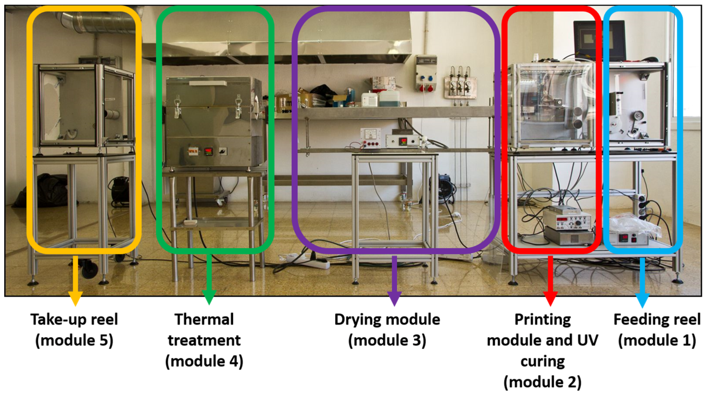
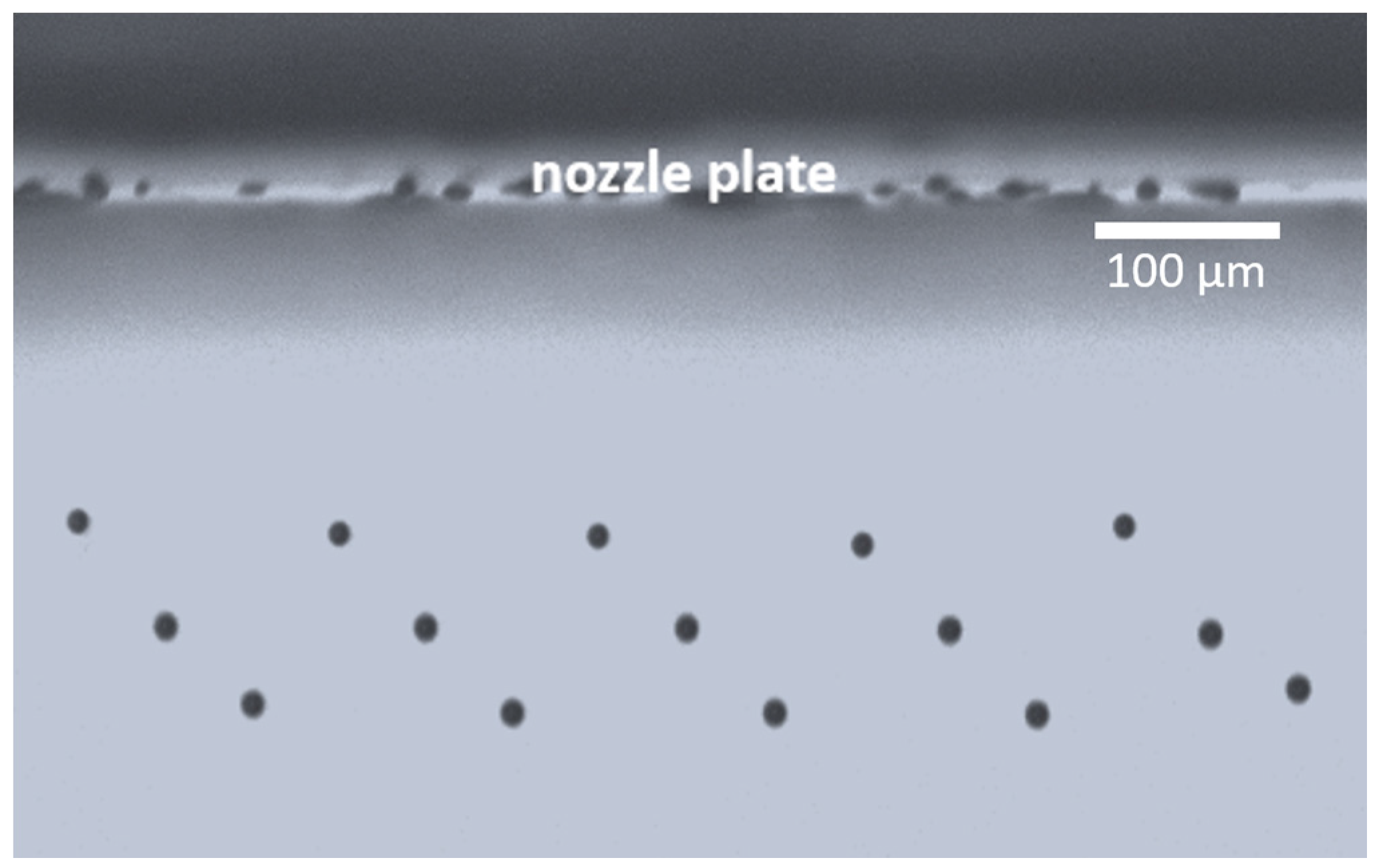
2.2.1. Metal-Organic Precursor Ink Deposition

Throughout this research, SDP-Y2O3 samples were deposited using the piezoelectric inkjet printing methodology [6,7] on top of unpolished stainless steel (SS) from Bruker (Alzenau, Germany) [42] previously wiped out with ethanol (99.8%, Sigma Aldrich, Saint Louis, MO, USA). In particular, inkjet printing was carried out using two kinds of printing set-ups: a batch printer and a roll to roll (R2R) inkjet printing continuous system. The first one is interesting because it represents an intermediate step between the lab scale and the R2R continuous approach and allows testing different printing and drying conditions in an easier and more practical way. Once these parameters have been screened in the batch printer, they are transferred to the continuous R2R line for the long-length functional oxide manufacturing. Both inkjet printing systems use the same Konica Minolta (KM) multinozzle piezoelectric printhead, composed of 512 nozzles, where drops are ejected after the deformation of small ink chambers made of a piezoelectric material. These 512 nozzles, divided into two rows of 256 nozzles, may be independently enabled or disabled. In our specific case, the KM512 printhead belongs to the M series, which corresponds to a nominal drop volume of 14 pL. For this multinozzle piezohead, drop volume was tailored by adjusting the compensation pressure, tuning the pulse width and amplitude of the piezoactuator waveform and also by optimizing the ink physicochemical properties such as the ink viscosity and the surface tension [8,43]. In the experiments presented along with this work, the drop volume ranged from 8.5 pL to 14 pL. The printhead is stationary during the printing deposition and the tape speed oscillates from 20 m/h to 44.5 m/h. The gap, i.e., the distance between the nozzle and the surface of the substrate, should be set, from one hand, large enough to obtain the spherical-like shaped drop after recoiling of the liquid thread before impacting on the surface and, from the other hand, as short as possible in order to prevent drop trajectory perturbations. During the printing experiments, it was set at about 1.5 mm.
For the up-scaling of these short-length SDP-Y2O3 samples, a pre-pilot R2R continuous inkjet printing plant was employed. The pre-pilot plant mainly consists of six modules (see Figure 1).
The substrate is placed in the feeding reel (Figure 1; module 1), then, it is introduced in the inkjet printing module (Figure 1; module 2) at an established speed. The tape speed, together with the drop density, i.e., number of drops per second, the drop volume and the ink concentration determine the final film thickness. Nowadays, tape speeds of about 100 m/h could be achieved in the present configuration of the pre-pilot plant. This module also contains a stroboscopic visualization system based on a LED (Light Emitting Diode) which flashes at the same frequency that drops are generated and a digital camera, which works in bright field mode.
The inkjet printing module includes a curing system in which through a UV lamp with an irradiation power between 0 mW and 5500 mW, the liquid will be pinned over the substrate.
Afterwards, the sample enters to the drying step (Figure 1; module 3) at temperatures ranging between 45 °C and 110 °C, where the partial solvent evaporation takes place. Following this drying stage, the sample goes through a furnace in which the pyrolysis process takes place, i.e., decomposition of the organic matter at temperatures between 300 °C and 500 °C and/or directly the sample is raised to higher temperatures (around 700–800 °C) to finally form the ceramic oxide in the desired phase (Figure 1; module 4). The final product is collected in a second exit reel (Figure 1; module 5).

2.2.2. Film Drying

After the inkjet deposition, the sample is dried using a resistance via thermal conduction to evaporate the low-boiling point solvents at temperatures ranging from 45 °C to 110 °C (module 3 of Figure 1).

2.2.3. Film Pyrolysis

As mentioned, the goal of the pyrolysis step is to remove the excess of solvent and decompose the organic matter, generating amorphous or nanocrystalline metallic precursors. Therefore, due to the decomposition of the organic compounds, a large fraction of precursor volume is eliminated during this step leading to strong film shrinkages. Internal stresses in plane to the substrate arisen in this shrinkage process may lead to films with cracks, buckling or other kind of defects [44].
Our pyrolysis process consisted of slowly heating the sample at heating rates from 3.7 °C/min to 17 °C/min to 500 °C in air during 2 h and 10 min in the tubular furnace shown in module 4 of Figure 1.

2.2.4. Film Characterization: Morphology, Microstructure and Texture

In this section, we briefly describe the equipment used to routinely characterize the SDP-Y2O3 films of this work. These include: morphological analysis by means of optical microscopy (OM), Focused Ion Beam (FIB) coupled with Scanning Electron Microscopy (SEM), (micro)structural characterization using X-ray Diffraction (XRD), surface topography characterization by means of Atomic Force Microscopy (AFM), thickness measurements by reflectometry and nanoindentation tests to evaluate the mechanical properties.
The surface homogeneity of the as-pyrolyzed coatings was normally investigated with an optical microscope. High resolution photographs were recorded through an Olympus (Shinjuku, Japan) BX51 microscope (5× and 10× objective) coupled to an Olympus DP20 camera.
Reflectometric measurements were acquired with a LS-DT2 light source from the FILMETRICS company (San Diego, CA, USA). In order to analyze the resulting spectra, we used the commercial software FILMeasure (version 7.0) from the FILMETRICS company.
SEM images were made using a ZEISS Merlin (Oberkochen, Germany), with an acceleration voltage of 2 kV.
Cross sectional images were obtained using a dual-beam scanning electron microscopy/focused-ion beam (SEM-FIB) system (Zeiss, Model 1560 XB, Oberkochen, Germany).
The θ–2θ spectra was done using a Siemens (Munich, Germany) D5000 diffractometer using a Cu-Kα radiation λ (Kα Cu = 1.5418 Å). Data acquisition was typically performed with a 0.02° step.
Two-dimensional X-ray (XRD2) studies presented in this work were done using the GADDS D8 Advance system from Bruker (Billerica, MA, USA), where GADDS stands for General Area Detector System [45].
The atomic force micrographs presented in this work were a with an Agilent 5100 AFM system from Agilent Technologies (Santa Clara, CA, USA). Images were taken in tapping mode and using silicon tips. Surface was typically scanned by the tip at 1 line/s. Scans of 20 × 20 μm2, 5 × 5 μm2 and 1 × 1 μm2 were performed at distinct zones of the sample. AFM images were processed with Mountains Map (version 7) software from Digital Surf (Besançon, France).
Nanoindentation experiments were performed using a Nanoindenter XP from MTS (Eden Prairie, MN, USA) equipped with a Berkovich tip. The maximum applied load was set to 1 mN. The nanoindentation function consisted of a loading segment, followed by a load holding segment and an unloading segment. The loading and unloading segments as well as the load holding segment were set to 10 s. The thermal drift was maintained below ±0.1 nm/s. From the load-displacement curves, the hardness and reduced Young’s modulus values were derived using the method of Oliver and Pharr [46]. The results were averaged over more than 40 indents for each sample to obtain statistically reliable data.

3. Results and Discussion

3.1. Inkjet Printing Deposition of Short-Length SDP-Y2O3 Films

The physicochemical and rheological properties of a 0.2 M ink (in yttrium; [DEA]/[Y] ratio of 4.5) were adjusted in terms of viscosity and wetting (Table 1). The printing parameters used in this work to deposit SDP-Y2O3 layers on top of unpolished stainless steel (SS) substrate from Bruker [42] are listed in Table 2 and graphically displayed in Figure 2. SDP-Y2O3 films of about 100 nm were prepared at tape speeds between 20 m/h and 44.5 m/h and pyrolyzed at 500 °C in air with the batch printer system.

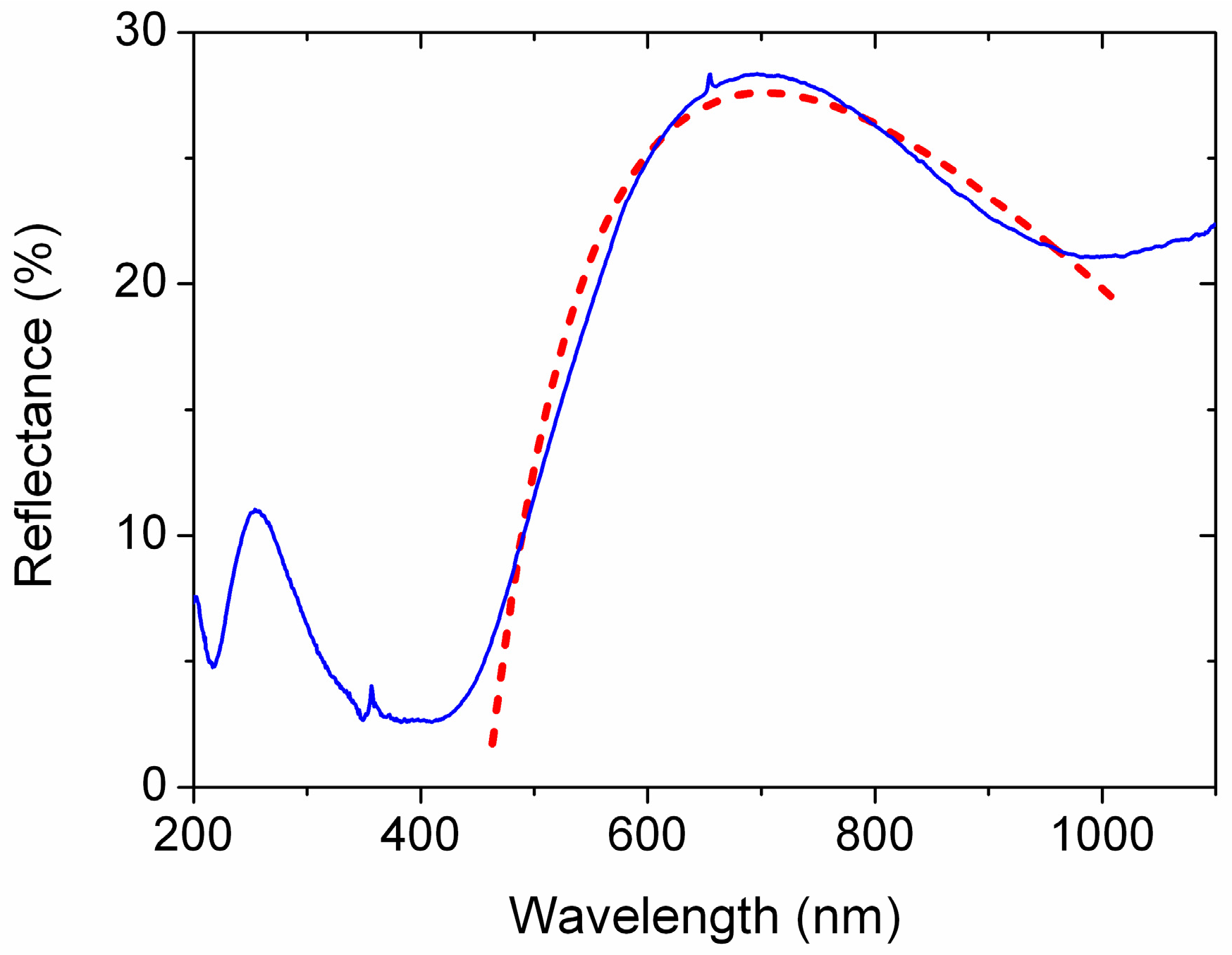
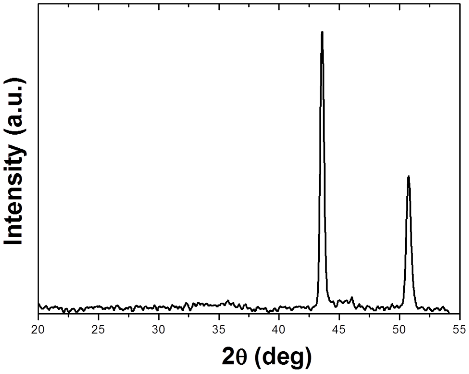
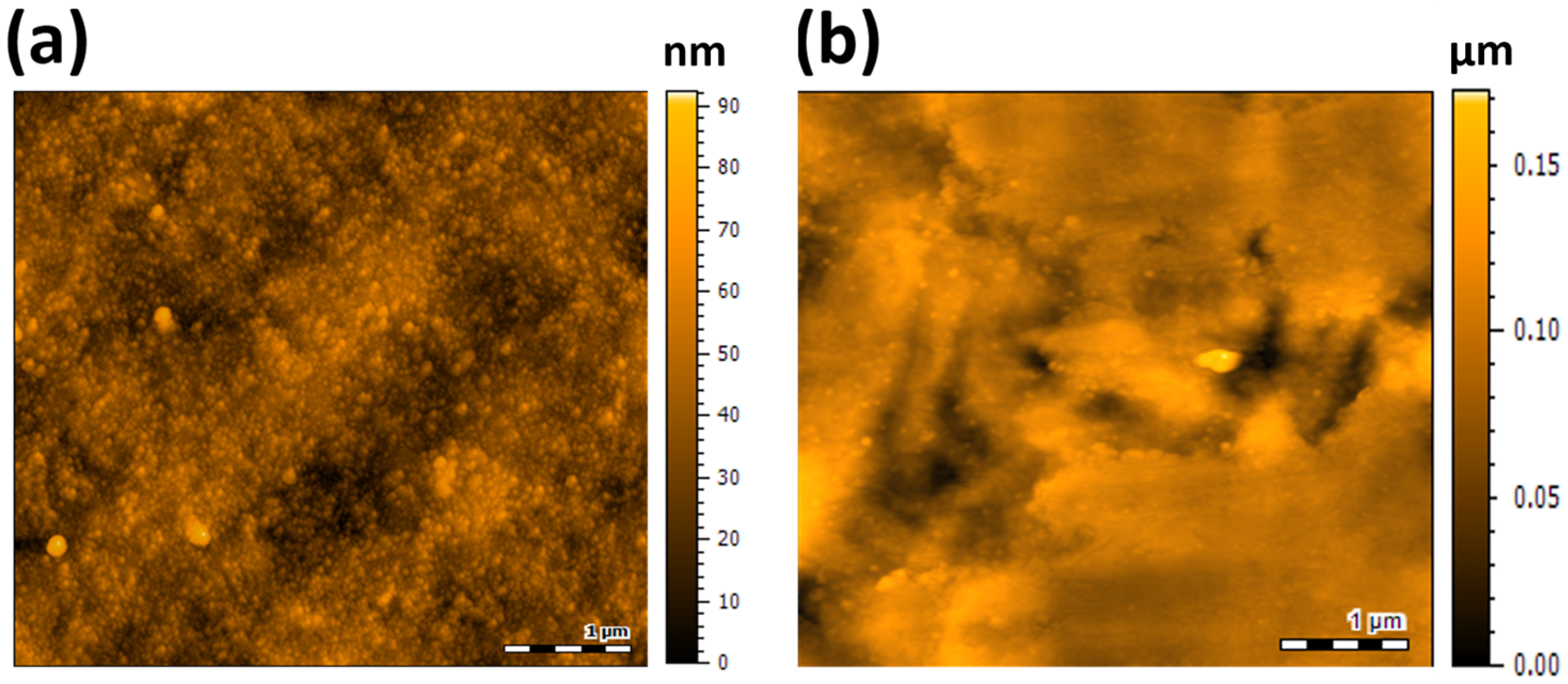
3.2. Characterization of Short-Length SDP-Y2O3 Films

Figure 3 exhibits a representative morphological characterization by optical microscopy of the central part (Figure 3a) and the edge (Figure 3b) of an ink-jetted SDP-Y2O3 film after pyrolysis in air at 500 °C. As may be observed in this Figure 3, the sample was continuous, fully covered in both longitudinal and transversal directions, without cracks or big pin holes. In the central region, the surface of the sample mainly displays only one color, indicating good homogeneity. However, by analyzing Figure 3b, although the whole surface is covered as well, a color grading is observed, which means that the thickness distribution along the transversal direction is not totally homogeneous. The yellow and the blue colors correspond to 100 nm and 90 nm respectively, confirmed by both reflectometry and profilometry techniques. This slight different thickness profile observed might be corrected by optimizing the printing matrix, i.e., distance between drops in both x- and y-directions and the ink formulation introducing some additives to modify the adhesion, the wettability and the evaporation rate of the solvents by pinning the liquid more efficiently.
To determine the macroscopic homogeneity of the sample and how this distribution of colors is correlated with thickness variations in the optical micrographs, Y2O3 layer thickness was monitored by reflectometry [47,48]. For each longitudinal point, at approximately each centimeter, three different spectra similar that the one presented in Figure 4 were taken along the 4 mm tape width. The averaged results are shown in the 2D color map of Figure 5. As may be observed, for both longitudinal and transversal directions, layer thickness ranges between 90 nm and 100 nm.
Figure 6a shows a more detailed characterization by SEM of the SDP-Y2O3 surface in which one can appreciate the sample’s low degree of porosity and the absence of cracks or buckling. Figure 6b exhibits the FIB cross sectional image of a SDP-Y2O3 film where the defects of the raw unpolished substrate are clearly covered by the SDP film above. Ag is added in order to avoid the charging of the sample as the film below is insulating.
After briefly reviewing the morphology of SDP-Y2O3 layers, the structural characterization of this SDP sample was performed by GADDS [45]. The non-existence of diffraction peaks corresponding to the Y2O3 phase in the XRD2 pattern indicates that after the pyrolysis step at 500 °C, Y2O3 phase is nanocrystalline. As it may be shown in Figure 7, two peaks are present at 2θ = 43.6° and 2θ = 50.7° corresponding to the unpolished SS substrate.
As these SDP-Y2O3 films must fill the defects present in the raw substrate while at the same time, act as template for the following buffer and superconducting layers, they are required to be as smooth as possible. Hence, the rms roughness of those SDP-Y2O3 samples was evaluated by Atomic Force Microscopy (AFM). Figure 8a shows an AFM topographic image of a single inkjet-deposited 100 nm thick SDP-Y2O3 film with rms roughness of 5.4 nm. For comparison, Figure 8b shows a topographical AFM image of the reference unpolished SS raw substrate from Bruker obtaining a rms roughness three times folder compared to the SDP-Y2O3 film, thus confirming the desired planarization effect by these solution derived SDP-Y2O3 films.

3.3. Printing on Smoother Substrates

To extrapolate this chemical method of planarization to substrates with different grades of polishing, a set of experiments combining different printing matrices and drying protocols were performed with the standard SDP ink formulation of Table 1. It was experimentally observed that when the rms roughness of the raw substrate is ≤10 nm, important macroscopic liquid movements were detected during the drying step or even just after the printing process leading to inhomogeneous coatings. Some approaches were attempted in order to pin the liquid and avoid such macroscopic liquid movements. Firstly, we tried to chemically activate the surface of the substrate by impregnation using a primer or by performing a plasma ozone treatment, increasing, in both cases, the work of adhesion [49,50]. None of these experimental options were enough to immobilize the liquid. Therefore, the next step was to slightly change the ink formulation. A photosensitive UV varnish from Kao-Chimigraf company (Rubí, Spain) [51] was introduced to the ink formulation with the aim of curing the as-deposited sample under UV irradiation (~395 nm) and therefore minimize such movements.
The physicochemical and rheological properties of the ink formulation with the photosensitive UV varnish are displayed in Table 3. This new ink formulation together with the tuned jetting and printing conditions displayed in Table 2 allows to obtain uniform and homogeneous samples on smoother substrates.
One of the trickiest aspects in the SDP deposition field is related with the stress generated during the Ion Beam Assisted Deposition (IBAD) process. These tensions may cause the delamination of the layers grown on top. In principle, stiffer films should give better resistance to the delamination.
To anticipate if a delamination process could occur when depositing the buffer layers, preliminary nanoindentation tests were performed in order to evaluate the mechanical properties of the resultant SDP-Y2O3 films.
Within this framework, nanoindentation tests were performed on the SDP-Y2O3 films prepared under two experimental conditions. The study was focused on evaluating if the precursor ink formulation, i.e., with or without UV photosensitive varnish, could have an effect on the final mechanical properties of the SDP-Y2O3 coatings simply by determining the hardness and Young’s modulus and studying the microstructure of the SDP-Y2O3 layers.
The red line with solid dots in Figure 9 shows a representative nanoindentation curve for a 100 nm SDP film printed using the standard formulation without varnish displayed in Table 1 and processed in air from 60 °C to 500 °C with a heating rate of 16 °C/min during 2 h and 10 min, while the blue triangles correspond to the 100 nm SDP film deposited from a UV varnish containing precursor ink processed the same time, temperature and heating rate than the SDP film of the dot solid red line. The empty square black line correlates to the unpolished SS raw substrate. A lower penetration depth at the maxim applied load (1 mN) is recorded for the film prepared without UV varnish thus indicating the harder nature of the layer. In Table 4, the values of hardness (H), reduced Young’s modulus (Er) and the ratio H/Er are listed for the different samples. In order to obtain reliable data when measuring the mechanical properties of thin films by nanoindentation, it is commonly accepted that the maximum penetration depth should be lower than 1/10th of the overall thickness of the film. Notice that the maximum penetration depth exceeds the 10% of the film thickness in our case. Thus, H and Er are influenced to some extent by the mechanical properties of the substrate. Nonetheless, from the nanoindentation results, it can be stated that the non-varnish-containing film exhibits larger hardness and larger reduced Young’s modulus than the film with varnish.
Of special importance is the ratio H/Er which is an indicative parameter of the wear resistance of the material [52,53]. The largest wear resistance value is observed for the film produced without varnish; hence, in terms of mechanical properties (i.e., wear resistance), this sample seems to better fulfil the mechanical requirements to accommodate other depositions on top without delamination.
The higher hardness and Young’s modulus of the SDP film which do not contains varnish in the ink formulation could be attributed to the dense microstructure without pores observed in the SEM micrography displayed in Figure 6a. On the contrary, the topographical SEM image of the SDP layer printed from an ink with UV varnish (Figure 10) shows a highly porous surface with low compacity. This high porosity could be directly related with the sample’s heating rate during the decomposition process at high temperatures and the content of this photosensitive UV component creating big pores in the structure. As regards, deeper studies are required to improve the final microstructure changing the processing dwell time and temperature, together with the tuning of the UV varnish content to know the mechanism, evolution and interrelation between these processing parameters, the mechanical properties (mainly H/Er) and the microstructure of the resultant SDP films to consequently avoid further delamination problems.

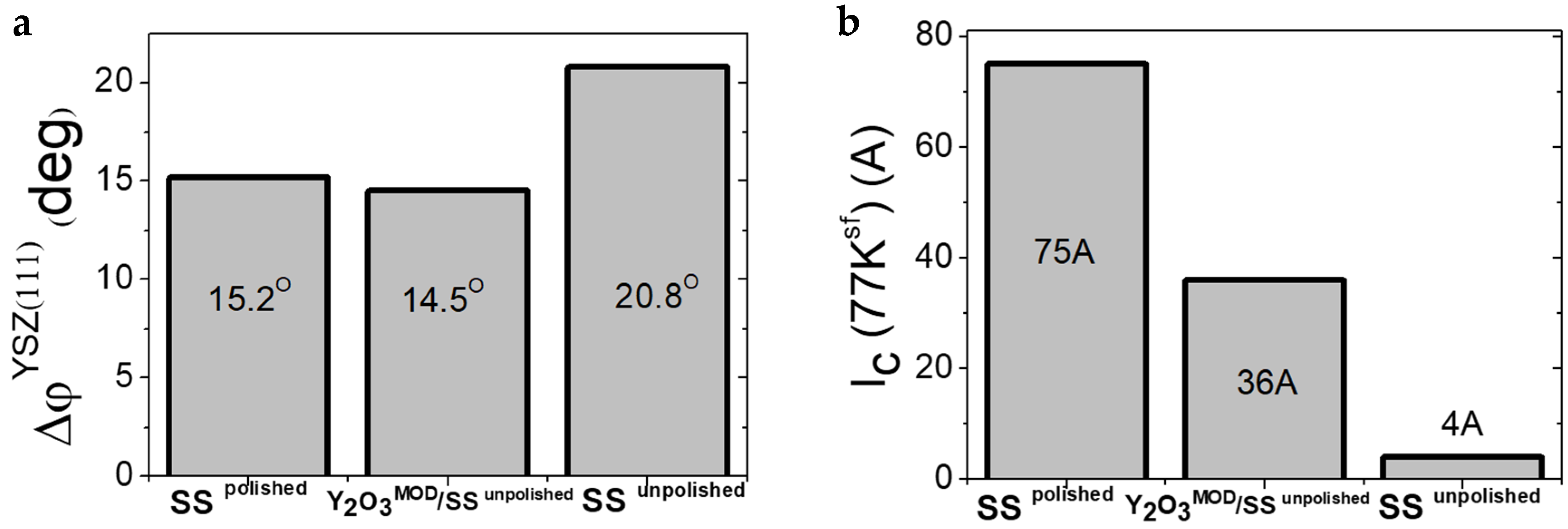
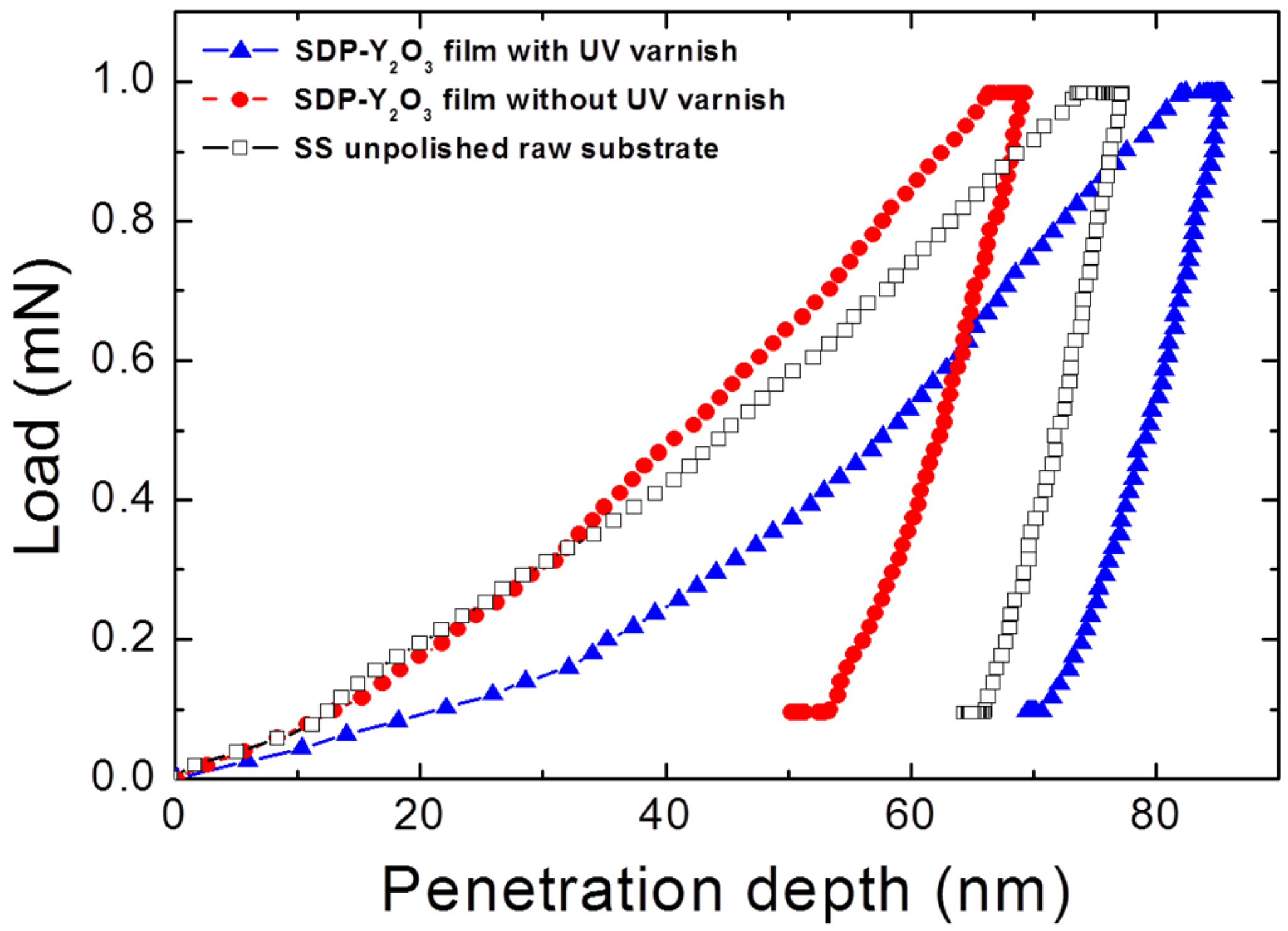
3.4. Validation of Short-Length SDP-Y2O3 Films

In order to value other substrate planarization methodologies as the low cost chemical solution deposition presented in this work, some short length samples, in the meter scale, were sent to Bruker HTS to deposit by ABAD between 800 nm and 1.1 µm of YSZ. Bruker was able to deposit 1.1 µm of YSZ on top of a 100 nm SDP-Y2O3 film without observing any kind of delamination on 100 nm SDP films from non-varnish based inks. The YSZ (111) in-plane texture was measured showing that 100 nm of this SDP-Y2O3 planarization layer allows better in-plane texture than on the SS polished reference (Figure 11a). Above these non-delaminated YSZ/SDP-Y2O3 samples, CeO2 and then YBCO were subsequently deposited by PLD obtaining, at the end, 50% of the critical intensity (Ic) as using the SS reference (Figure 11b). Much effort is required to increase this Ic value tuning the deposition and thermal processes to enhance Ic up to, at least, the polished SS reference.

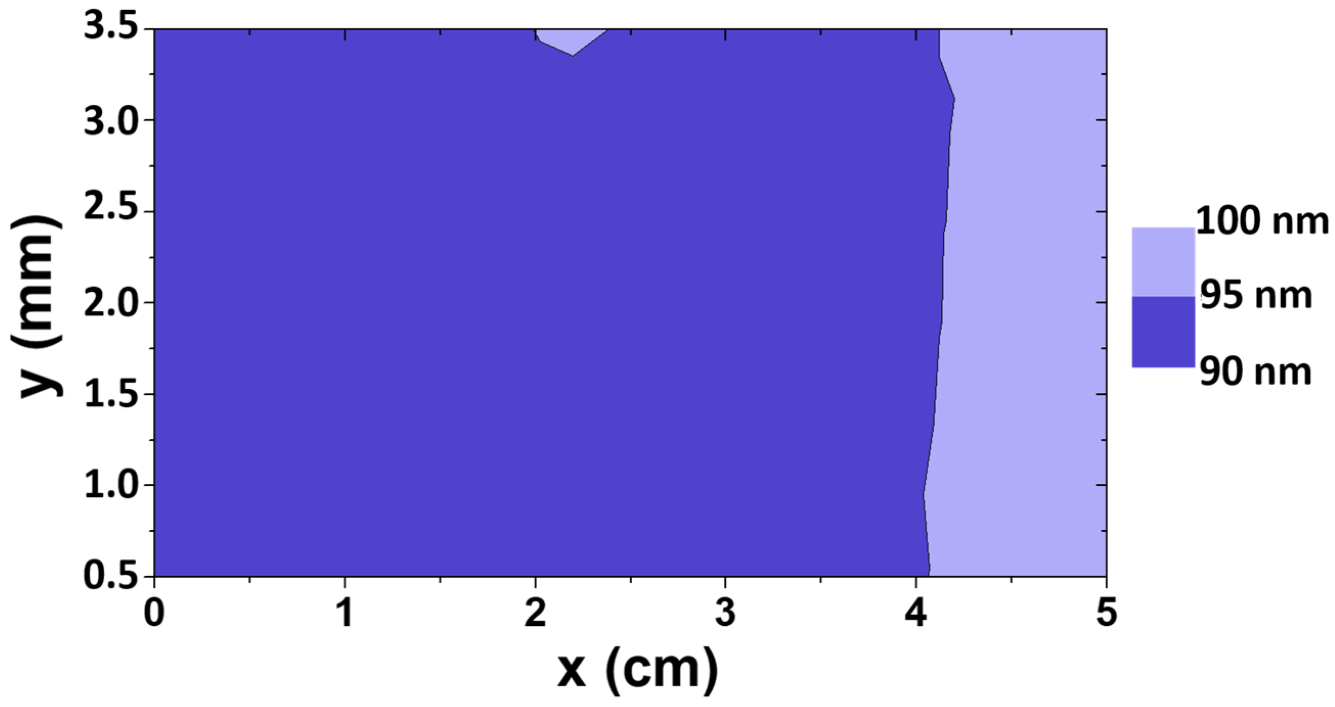
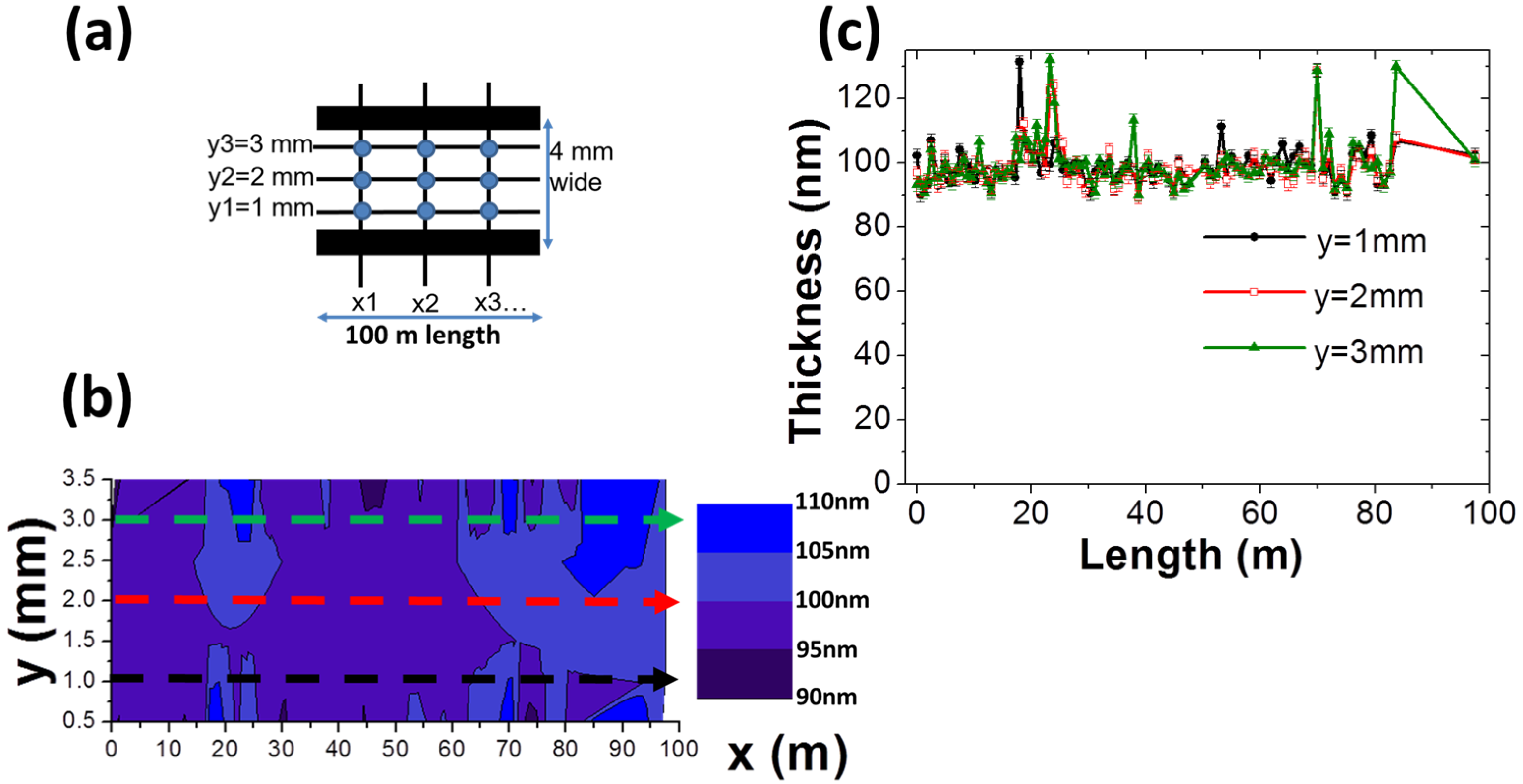
3.5. Scale-up of the SDP-Y2O3 Films

After a correct tuning of the ink formulation, together with an adequate reel correction based on the reel diameter and a suitable liquid height compensation, SDP-Y2O3 films were scaled in a medium scale. 100 m of uniform and homogeneous SDP layer without cracks on unpolished stainless steel substrate from Bruker were obtained at a tape speed of 44.5 m/h and pyrolyzed in air at 500 °C. Figure 12 shows a complete characterization along the length by optical microscopy displaying longitudinal homogeneity from the beginning to the end. In those blue and yellow regions, the thickness oscillates between 90 nm and 110 nm.
The design of the reflectometric measurements and the study of the thickness evolution over the length are presented in Figure 13a,b. Figure 13b displays the 2D color-coded thickness map for the 100 m length SDP-Y2O3 sample.
The longitudinal analysis at 1, 2 and 3 mm from the bottom-up edges gives an average thickness of about 100 nm from end to end as might be appreciated in Figure 13c.

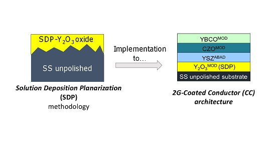
4. Summary and Conclusions

In the present research, we have first reviewed the feasibility to obtain cm length SDP-Y2O3 films by proper adjustments of the ink properties, printing and drying protocols using a piezoelectric drop-on-demand inkjet printer mounted in both batch and R2R continuous inkjet printing systems.
We have also reported on the scalability of the complete R2R process by preparing 100 m length SDP-Y2O3 on unpolished SS substrate which definitely represents a new breakthrough advancement in the field of high quality biaxially textured conductors. The morphological characterization gives continuous and uniform films with average thickness around 100 nm confirmed both by reflectometry and profilometry.
The addition of the planarization layer is beneficial for the texture development during the ABAD texturing process and it yields 50% of Ic with respect to the standard SS substrate. The optimization of the thermal pyrolysis process is crucial in order to increase this Ic value up to, at least, the SS polished reference.
A second advancement reported in this work arises from the printing on smoother substrates (rms roughness on 5 × 5 µm2 area ≤ 10 nm) which forced to develop an alternative UV photosensitive varnish-containing ink. This new UV varnish-based ink is essential to pin the liquid on the surface after the jetting and drying stages. Nevertheless, although these SDP layers are longitudinally uniform, considerable effort has to be devoted to further improve the final microstructure when using this UV varnish by tuning the processing conditions as the dwell time, temperature and the content of the UV varnish, which could help to know the bonds between the mechanical properties, processing variables and the final microstructure of such SDP-Y2O3 films, possibly eluding the delamination of the ceramic tapes grown above. This new ink formulation offers more versatility and flexibility to print on substrates with different grades of polishing as it could not be achieved with the first mentioned ink formulation of Table 1.
In conclusion, Solution Deposition Planarization (SDP) methodology represents an outstanding methodology to decrease the final cost of the fabrication of 2G wire coated conductors (CC’s) based on the strong attractiveness from the cost point of view remaining as a powerful area of interest in the area of CC’s.

Acknowledgments

The authors would like to acknowledge the financial support from the European project EUROTAPES FP7-NMP-Large-2011-280432, the national project SUPERINKS (RTC-2015-3640-3) and also the financial support from Spanish government through the “Severo Ochoa” Programme (SEV-2015-0496), CONSOLIDER Excellence Network (MAT2015-68994-REDC) and COACHSUPENERGY project (MAT2014-51778-C2-1-R, co-financed by the European Regional Development Fund).

Author Contributions

Marta Vilardell wrote the paper, defined and performed the printing experiments and the morphological characterization. Jordina Fornell designed, performed and interpreted the nanoindentation tests. Jordi Sort contributed to the discussion of the nanoindentation results. Roxana Vlad analyzed the reflectometric data. Juan Carlos Fernández and Joaquim Puig contributed to the development of the UV-photosensitive ink formulation. Alexander Usoskin designed the ABAD/YSZ experiments and performed the texture and superconducting measurements of the complete architecture. Anna Palau performed the FIB-SEM measurements. Teresa Puig, Xavier Obradors and Albert Calleja collaborated in the discussion of the technical results.

Conflicts of Interest

The authors declare no conflict of interest.

References

  1. Sascha, K.; Paul, N.A.; Coulter, J.Y.; Paul, C.D.; Stephen, R.F.; Brady, J.G.; Vladimir, M.; Chris, J.S. Reel-to-reel preparation of ion-beam assisted deposition (IBAD)-MgO based coated conductors. Supercond. Sci. Technol. 2004, 17, S132–S134. [Google Scholar] [CrossRef]
  2. Lange, F.F. Chemical Solution Routes to Single-Crystal Thin Films. Science 1996, 273, 903–909. [Google Scholar] [CrossRef] [PubMed]
  3. Schwartz, R.W. Chemical Solution Deposition of Perovskite Thin Films. Chem. Mater. 1997, 9, 2325–2340. [Google Scholar] [CrossRef]
  4. Schwartz, R.W.; Schneller, T.; Waser, R. Chemical solution deposition of electronic oxide films. Comptes Rendus Chim. 2004, 7, 433–461. [Google Scholar] [CrossRef]
  5. Obradors, X.; Puig, T.; Pomar, A.; Sandiumenge, F.; Mestres, N.; Coll, M.; Cavallaro, A.; Romà, N.; Gázquez, J.; González, J.C.; et al. Progress towards all-chemical superconducting YBa2Cu3O7-coated conductors. Supercond. Sci. Technol. 2006, 19, S13–S26. [Google Scholar] [CrossRef]
  6. Derby, B. Inkjet Printing of Functional and Structural Materials: Fluid Property Requirements, Feature Stability and Resolution. Annu. Rev. Mater. Res. 2010, 40, 395–414. [Google Scholar] [CrossRef]
  7. Wijshoff, H. The dynamics of the piezo inkjet printhead operation. Phys. Rep. 2010, 491, 77–177. [Google Scholar] [CrossRef]
  8. Dong, H.; Carr, W.W.; Morris, J.F. An experimental study of drop-on-demand drop formation. Phys. Fluids 2006, 18, 072102. [Google Scholar] [CrossRef]
  9. Vilardell, M.; Granados, X.; Ricart, S.; van Driessche, I.; Palau, A.; Puig, T.; Obradors, X. Flexible manufacturing of functional ceramic coatings by inkjet printing. Thin Solid Films 2013, 548, 489–497. [Google Scholar] [CrossRef]
  10. Feys, J.; Vermeir, P.; Lommens, P.; Hopkins, S.C.; Granados, X.; Glowacki, B.A.; Baecker, M.; Reich, E.; Ricard, S.; Holzapfel, B.; et al. Ink-jet printing of YBa2Cu3O7 superconducting coatings and patterns from aqueous solutions. J. Mater. Chem. 2012, 22, 3717–3726. [Google Scholar] [CrossRef]
  11. Larbalestier, D.; Gurevich, A.; Feldmann, D.M.; Polyanskii, A. High-Tc superconducting materials for electric power applications. Nature 2001, 414, 368–377. [Google Scholar] [CrossRef] [PubMed]
  12. MacManus-Driscoll, J.L. Recent developments in conductor processing of high irreversibility field superconductors. Annu. Rev. Mater. Sci. 1998, 28, 421–462. [Google Scholar] [CrossRef]
  13. Rogalla, H.; Kes, P.H. 100 Years of Superconductivity; CRC Press Taylor & Francis Group: Boca Raton, FL, USA, 2011. [Google Scholar]
  14. Obradors, X.; Puig, T. Coated conductors for power applications: Materials challenges. Supercond. Sci. Technol. 2014, 27, 044003. [Google Scholar] [CrossRef]
  15. Lee, S.; Petrykin, V.; Molodyk, A.; Samoilenkov, S.; Kaul, A.; Vavilov, A.; Vysotsky, V.; Fetisov, S. Development and production of second generation high Tc superconducting tapes at SuperOx and first tests of model cables. Supercond. Sci. Technol. 2014, 27, 044022. [Google Scholar] [CrossRef]
  16. Iijima, Y.; Kakimoto, K.; Yamada, Y.; Izumi, T.; Saitoh, T.; Shiohara, Y. Research and Development of Biaxially Textured IBAD-GZO Templates for Coated Superconductors. MRS Bull. 2004, 29, 564–571. [Google Scholar] [CrossRef]
  17. Goyal, A.; Paranthaman, M.P.; Schoop, U. The RABiTS Approach: Using Rolling-Assisted Biaxially Textured Substrates for High-Performance YBCO Superconductors. MRS Bull. 2004, 29, 552–561. [Google Scholar] [CrossRef]
  18. Paranthaman, M.P.; Aytug, T.; Zhai, H.Y.; Heatherly, L.; Goyal, A.; Christen, D.K. Growth of YBCO films on MgO-based rolling-assisted biaxially textured substrates templates. Supercond. Sci. Technol. 2005, 18, 223–228. [Google Scholar] [CrossRef]
  19. Usoskin, A.; Kirchhoff, L. In-Plane Texturing of Buffer Layers by Alternating Beam Assisted Deposition: Large Area and Small Area Applications; Cambridge University Press: New York, NY, USA, 2008; Volume 1150. [Google Scholar] [CrossRef]
  20. Hassini, A.; Pomar, A.; Gutiérrez, J.; Coll, M.; Romà, N.; Moreno, C.; Ruyter, A.; Puig, T.; Obradors, X. Atomically flat MOD La0.7Sr0.3MnO3 buffer layers for high critical current YBa2 Cu3O7 TFA films. Supercond. Sci. Technol. 2007, 20, S230–S238. [Google Scholar] [CrossRef]
  21. Usoskin, A.; Betz, U.; Dietrich, R.; Schlenga, K. Long HTS Coated Conductor Processed via Large-Area PLD/ABAD for High-Field Applications. IEEE Trans. Appl. Supercond. 2016, 26, 1–4. [Google Scholar] [CrossRef]
  22. Samoilenkov, S.; Molodyk, A.; Lee, S.; Petrykin, V.; Kalitka, V.; Martynova, I.; Makarevich, A.; Markelov, A.; Moyzykh, M.; Blednov, A. Customised 2G HTS wire for applications. Supercond. Sci. Technol. 2016, 29, 024001. [Google Scholar] [CrossRef]
  23. Bhuiyan, M.S.; Paranthaman, M.; Sathyamurthy, S.; Aytug, T.; Kang, S.; Lee, D.F.; Goyal, A.; Payzant, E.A.; Salama, K. MOD approach for the growth of epitaxial CeO2 buffer layers on biaxially textured Ni–W substrates for YBCO coated conductors. Supercond. Sci. Technol. 2003, 16, 1305–1309. [Google Scholar] [CrossRef]
  24. Engel, S.; Knoth, K.; Hühne, R.; Schultz, L.; Holzapfel, B. An all chemical solution deposition approach for the growth of highly textured CeO2 cap layers on La2Zr2O7-buffered long lengths of biaxially textured Ni–W substrates for YBCO-coated conductors. Supercond. Sci. Technol. 2005, 18, 1385–1390. [Google Scholar] [CrossRef]
  25. Yang, C.; He, Y.Y.; Chu, J.W.; Xue, Y.; Zhang, F.; Hui, W.; Tao, B.W.; Xiong, J. Tailoring surface roughness of LaMnO3 buffer layers for YBCO-coated conductors. Rare Met. 2015, 34, 859–863. [Google Scholar] [CrossRef]
  26. Wang, Y.; Li, C.; Feng, J.; Yu, Z.; Jin, L.; Zhang, P. Epitaxial growth of CSD modified lanthanum zirconium oxide buffer layer for coated conductors. J. Alloys Compd. 2016, 682, 424–431. [Google Scholar] [CrossRef]
  27. Hühne, R.; Güth, K.; Gärtner, R.; Kidszun, M.; Thoss, F.; Rellinghaus, B.; Schultz, L.; Holzapfel, B. Application of textured IBAD-TiN buffer layers in coated conductor architectures. Supercond. Sci. Technol. 2010, 23, 014010. [Google Scholar] [CrossRef]
  28. Dürrschnabel, M.; Aabdin, Z.; Große, V.; Bauer, M.; Sigl, G.; Prusseit, W.; Eibl, O. Growth of Biaxially-Textured MgO Buffer Layers by Inclined Substrate Deposition. Phys. Procedia 2012, 36, 1546–1551. [Google Scholar] [CrossRef]
  29. Xiong, J.; Xue, Y.; Xia, Y.D.; Zhang, F.; Zhang, Y.X.; Li, L.H.; Zhao, X.H.; Tao, B.W. Fabrication of long-length ion beam-assisted deposited MgO templates for YBCO-coated conductors. Rare Met. 2013, 32, 574–578. [Google Scholar] [CrossRef]
  30. Paranthaman, M.P.; Tolga, A.; Liliana, S.; Quanxi, J.; Claudia, C.; Wee, S.H. Chemical solution derived planarization layers for highly aligned IBAD-MgO templates. Supercond. Sci. Technol. 2014, 27, 022002. [Google Scholar] [CrossRef]
  31. Shi, X.; Rock, S.E.; Turk, M.C.; Roy, D. Minimizing the effects of galvanic corrosion during chemical mechanical planarization of aluminum in moderately acidic slurry solutions. Mater. Chem. Phys. 2012, 136, 1027–1037. [Google Scholar] [CrossRef]
  32. Jia, Q.; Wang, Y.; Suo, H.L.; Wang, P.; Li, M.Y.; Huo, Q.Y. Electropolishing technique of Hastelloy C-276 alloy. Rare Met. 2017, 36, 635–639. [Google Scholar] [CrossRef]
  33. Wang, X.; Li, C.; Yu, Z.; Zheng, H.; Ji, Y.; Ji, P.; Chen, Z.; Fan, Z. Electropolishing of Ni–5 at.% W substrates for YBCO coated conductors. Mat. Chem. Phys. 2012, 133, 212–217. [Google Scholar] [CrossRef]
  34. Sheehan, C.; Jung, Y.; Holesinger, T.; Feldmann, D.M.; Edney, C.; Ihlefeld, J.F.; Clem, P.G.; Matias, V. Solution deposition planarization of long-length flexible substrates. Appl. Phys. Lett. 2011, 98, 071907. [Google Scholar] [CrossRef]
  35. Martynova, I.A.; Tsymbarenko, D.M.; Kamenev, A.A.; Mudretsova, S.N.; Streletsky, A.N.; Vasiliev, A.L.; Kuzmina, N.P.; Kaul, A.R. Chemical deposition of smooth nanocrystalline Y2O3 films from solutions of metal-organic precursors. Russ. Chem. Bull. 2013, 62, 1454–1458. [Google Scholar] [CrossRef]
  36. Martynova, I.; Tsymbarenko, D.; Kamenev, A.; Amelichev, V.; Molodyk, A.; Kuzmina, N.; Kaul, A. Solution deposition of ultrasmooth alumina on long-length metallic substrate for 2G superconducting tapes. Mater. Res. Bull. 2016, 78, 64–71. [Google Scholar] [CrossRef]
  37. Smith, P.J. The Chemistry of InkJet Inks; World Scientific: Singapore, 2010; pp. 55–72. [Google Scholar]
  38. Anastasiadis, S.H.; Chen, J.K.; Koberstein, J.T.; Siegel, A.F.; Sohn, J.E.; Emerson, J.A. The determination of interfacial tension by video image processing of pendant fluid drops. J. Colloid Interface Sci. 1987, 119, 55–66. [Google Scholar] [CrossRef]
  39. Girault, H.H.J.; Schiffrin, D.J.; Smith, B.D.V. The measurement of interfacial tension of pendant drops using a video image profile digitizer. J. Colloid Interface Sci. 1984, 101, 257–266. [Google Scholar] [CrossRef]
  40. Rotenberg, Y.; Boruvka, L.; Neumann, A.W. Determination of surface tension and contact angle from the shapes of axisymmetric fluid interfaces. J. Colloid Interface Sci. 1983, 93, 169–183. [Google Scholar] [CrossRef]
  41. Boyce, J.F.; Schürch, S.; Rotenberg, Y.; Neumann, A.W. The measurement of surface and interfacial tension by the axisymmetric drop technique. Colloids Surf. 1984, 9, 307–317. [Google Scholar] [CrossRef]
  42. Usoskin, A.; Kirchhoff, L.; Knoke, J.; Prause, B.; Rutt, A.; Selskij, V.; Farrell, D.E. Processing of Long-Length YBCO Coated Conductors Based on Stainless Steel Tapes. IEEE Trans. Appl. Supercond. 2007, 17, 3235–3238. [Google Scholar] [CrossRef]
  43. Jang, D.; Kim, D.; Moon, J. Influence of fluid physical properties on ink-jet printability. Langmuir 2009, 25, 2629–2635. [Google Scholar] [CrossRef] [PubMed]
  44. Kozuka, H.; Takenaka, S.; Tokita, H.; Hirano, T.; Higashi, Y.; Hamatani, T. Stress and Cracks in Gel-Derived Ceramic Coatings and Thick Film Formation. J. Sol-Gel Sci. Technol. 2003, 26, 681–686. [Google Scholar] [CrossRef]
  45. He, B.B. Two-Dimensional X-ray Diffraction; John Wiley & Sons: Hoboken, NJ, USA, 2009. [Google Scholar]
  46. Fischer-Cripps, A.C. Nanoindentation; Springer: New York, NY, USA, 2002. [Google Scholar]
  47. Chet, L.; Furse, C. Noise-domain reflectometry for locating wiring faults. IEEE Trans. Electromagn. Compat. 2005, 47, 97–104. [Google Scholar] [CrossRef]
  48. Jenkins, F.A.; White, H.E. Fundamentals of Optics; McGraw-Hill: New York, NY, USA, 1957; pp. 464–487. [Google Scholar]
  49. Chibowski, E. On some relations between advancing, receding and Young’s contact angles. Adv. Colloid Interface Sci. 2007, 133, 51–59. [Google Scholar] [CrossRef] [PubMed]
  50. Ström, G.; Fredriksson, M.; Stenius, P. Contact angles, work of adhesion and interfacial tensions at a dissolving Hydrocarbon surface. J. Colloid Interface Sci. 1987, 119, 352–361. [Google Scholar] [CrossRef]
  51. Marcè, A.; Fernández, J.C.; Chimigraf Ibérica, S.L. Method for Producing a Digital Inkjet Printing Ink and Thus Obtained Digital Inkjet Printing Ink; WO 2017/158217 A1; WIPO: Geneva, Switzerland, 2017. [Google Scholar]
  52. Leyland, A.; Matthews, A. On the significance of the H/E ratio in wear control: A nanocomposite coating approach to optimised tribological behaviour. Wear 2000, 246, 1–11. [Google Scholar] [CrossRef]
  53. Rebholz, C.; Leyland, A.; Schneider, J.M.; Voevodin, A.A.; Matthews, A. Structure, hardness and mechanical properties of magnetron-sputtered titanium–aluminium boride films. Surf. Coat. Technol. 1999, 120, 412–417. [Google Scholar] [CrossRef]
Figure 1. General photograph of the R2R continuous pre-pilot plant to deposit functional ceramic oxides by inkjet printing.
Coatings 07 00227 g001
Figure 2. Typical jetting drop distribution of a 0.2 M (in yttrium) SDP-Y2O3 precursor ink and [DEA]/[Y] ratio of 4.5 after the tuning of the waveform excitation parameters displayed in Table 2.
Coatings 07 00227 g002
Figure 3. Typical optical micrographs of a 5 cm ink-jetted SDP-Y2O3 film. The sample was printed at a tape speed of 35 m/h and pyrolyzed at a heating ramp of 3.7 °C/min up to 500 °C (a) Central part and (b) Edge of the SDP-Y2O3 film.
Coatings 07 00227 g003
Figure 4. Spectrum of a pyrolyzed ink-jetted SDP-Y2O3 film on unpolished SS tape obtained by reflectometry. The solid blue line is the measured experimental spectrum, while the dashed red line is the theoretical fitting provided by the software.
Coatings 07 00227 g004
Figure 5. Colored-coded thickness map of a typical 5 cm length SDP-Y2O3 sample. The averaged thickness fluctuates between 90 nm and 100 nm. Measurements were taken each cm in the longitudinal direction and three measurements were acquired in the transversal direction. The diameter of the reflectometer’s spot is 1 mm. Edges were avoided in the reflectometric measurements.
Coatings 07 00227 g005
Figure 6. Microstructural characterization of the previous pyrolyzed ink-jetted SDP-Y2O3 film. (a) SEM micrograph where no pores neither cracks are present; (b) FIB cross sectional image which allows confirming the coverage of the defects of the raw metallic substrate underneath.
Coatings 07 00227 g006
Figure 7. Structural XRD characterization of a 100 nm thick SDP-Y2O3 coating by GADDS (2D detector) showing only the peaks of the SS substrate.
Coatings 07 00227 g007
Figure 8. AFM topographical analysis of the surface of (a) a 100 nm SDP-Y2O3 film (b) the reference unpolished stainless steel raw substrate provided directly from Bruker HTS.
Coatings 07 00227 g008
Figure 9. Nanoindentation curves for the SDP-Y2O3 films with and without UV varnish (triangle solid blue line and dot solid red line, respectively) and the SS unpolished raw substrate (empty black square line).
Coatings 07 00227 g009
Figure 10. SEM micrography of a film deposited from a 0.2 M (in Y) SDP precursor ink with a 10% (v/v) of the UV varnish and [DEA]/[Y] ratio of 4.5.
Coatings 07 00227 g010
Figure 11. Comparison of texture and superconducting properties between the SSpolished, the SSunpolished and the SS/SDP-Y2O3CSD/YSZABAD/CeO2PLD/YBCOPLD stack. (a) ϕ scan representing the texture measurements of the SSpolished, the SSunpolished and the SS/SDP-Y2O3CSD/YSZABAD sandwich architecture; (b) Critical current intensity (Ic) measurements of the different type of substrates in comparison to the SDP-Y2O3 planarization film.
Coatings 07 00227 g011
Figure 12. Optical characterization of the 100 m length SDP-Y2O3 sample. From the top left to the bottom right correspond to the sequential optical characterization of the 100 m length SDP-Y2O3. Each micrograph was approximately taken each 7 cm.
Coatings 07 00227 g012
Figure 13. Reflectometric analysis of the 100 m long-length SDP-Y2O3 film. (a) Design of the reflectometric studies; (b) Colored-coded thickness map of this 100 m length SDP-Y2O3 sample; (c) Longitudinal thickness analysis at 1, 2 and 3 mm from the edge of the tape. Edges were avoided in the reflectometric measurements. Measurements were taken each cm in the longitudinal direction and three measurements were acquired in the 4 mm wide tape. The diameter of the spot is 1 mm.
Coatings 07 00227 g013
Table 1. Relevant physicochemical and rheological properties of a 0.2 M (in yttrium) SDP-Y2O3 precursor ink with a [DEA]/[Y] ratio of 4.5. Viscosity measurement was carried out at a shear rate of 2880 s−1 and 25 °C. The contact angle was measured at room temperature on top of unpolished stainless steel from Bruker.
Ink Physicochemical and Rheological PropertiesValue
Density (g/cm3)0.915 ± 0.018
Surface tension (mN/m)24.7 ± 0.3
Viscosity (mPa·s)7.7 ± 0.5
Contact angle (°)25 ± 2
Table 2. Jetting parameters used to obtain the SDP-Y2O3 films shown in Figure 3. The printhead used was a piezo 512 Konika Minolta (Chiyoda, Japan) head type M and the SDP-Y2O3 precursor ink was a 0.2 M (in yttrium) with a [DEA]/[Y] ratio of 4.5.
Jetting ParametersValue
High pulse width (µs) 6.4
High-low pulse delay (µs)0
Drop period (µs)32
Low pulse width (µs)12.8
Phase length (µs)32.6
Voltage up (V)11.4
Voltage down (V)5.7
Printhead Temperature (°C)25
Table 3. Relevant physicochemical properties of a 0.2 M (in yttrium) SDP-Y2O3 precursor ink ([DEA]/[Y] ratio of 4.5) with a 10% (v/v) of UV photosensitive varnish. Viscosity measurement was carried out at a shear rate of 2880 s−1 and 25 °C. The contact angle was measured at room temperature on top of unpolished SS from Bruker.
Ink Physicochemical and Rheological PropertiesValue
Density (g/cm3)0.927 ± 0.015
Surface tension (mN/m)25.4 ± 0.2
Viscosity (mPa·s)7.7 ± 0.5
Contact angle (°)27 ± 2
Table 4. Mechanical properties of the unpolished SS raw substrate and 100 nm thick SDP-Y2O3 films deposited from inks with and without UV varnish.
Mechanical Parameters at 1 mNSDP-Y2O3 Film without UV VarnishSDP-Y2O3 Film with UV VarnishSS Unpolished Substrate
Hardness H (GPa)8.5 ± 0.55.2 ± 1.86.2 ± 1.1
Reduced Young modulus Er (GPa)202 ± 15177 ± 45234 ± 26
H/Er0.0420.0250.026

