
Photonic Structures for Light Trapping in Thin Film Silicon Solar Cells: Design and Experiment


1
Institute of Photoelectronic Thin Film Devices & Technology, Nankai University, Tianjin 300071, China
2
Key Laboratory of Photoelectronic Thin Film Devices & Technology of Tianjin, Nankai University, Tianjin 300071, China
3
Key Laboratory of Optical Information Science & Technology, Ministry of Education, Nankai University, Tianjin 300350, China
4
School of Electrical Engineering and Automation, Tianjin Polytechnic University, Tianjin 300387, China
5
Department of Electrical and Computer Engineering, Michigan State University, East Lansing, MI 48824, USA
*
Author to whom correspondence should be addressed.
Coatings 2017, 7(12), 236; https://doi.org/10.3390/coatings7120236
Submission received: 27 October 2017
/
Revised: 12 December 2017
/
Accepted: 12 December 2017
/
Published: 21 December 2017
(This article belongs to the Special Issue Plasma Etching and Deposition)
Abstract
:One of the foremost challenges in designing thin-film silicon solar cells (TFSC) is devising efficient light-trapping schemes due to the short optical path length imposed by the thin absorber thickness. The strategy relies on a combination of a high-performance back reflector and an optimized texture surface, which are commonly used to reflect and scatter light effectively within the absorption layer, respectively. In this paper, highly promising light-trapping structures based on a photonic crystal (PC) for TFSCs were investigated via simulation and experiment. Firstly, a highly-reflective one-dimensional photonic crystal (1D-PC) was designed and fabricated. Then, two types of 1D-PC-based back reflectors (BRs) were proposed: Flat 1D-PC with random-textured aluminum-doped zinc oxide (AZO) or random-textured 1D-PC with AZO. These two newly-designed BRs demonstrated not only high reflectivity and sufficient conductivity, but also a strong light scattering property, which made them efficient candidates as the electrical contact and back reflector since the intrinsic losses due to the surface plasmon modes of the rough metal BRs can be avoided. Secondly, conical two-dimensional photonic crystal (2D-PC)-based BRs were investigated and optimized for amorphous a-SiGe:H solar cells. The maximal absorption value can be obtained with an aspect ratio of 1/2 and a period of 0.75 µm. To improve the full-spectral optical properties of solar cells, a periodically-modulated PC back reflector was proposed and experimentally demonstrated in the a-SiGe:H solar cell. This periodically-modulated PC back reflector, also called the quasi-crystal structure (QCS), consists of a large periodic conical PC and a randomly-textured Ag layer with a feature size of 500–1000 nm. The large periodic conical PC enables conformal growth of the layer, while the small feature size of Ag can further enhance the light scattering. In summary, a comprehensive study of the design, simulation and fabrication of 1D-PC- and 2D-PC-based back reflectors for TFSCs was carried out. Total absorption and device performance enhancement were achieved with the novel PC light-trapping systems because of their high reflectivity or high scattering property. Further research is necessary to illuminate the optimal structure design of PC-based back reflectors and high solar cell efficiency.
1. Introduction
Efficiency improvement and cost reduction are everlasting schemes for photovoltaic (PV) research and development. Although the current PV market is dominated by crystalline silicon (c-Si) solar cells because of their high efficiency and steadily decreasing manufacturing cost [1,2], thin-film silicon solar cells (TFSC) including hydrogenated amorphous silicon (a-Si:H), amorphous silicon germanium (a-SiGe:H) and microcrystalline silicon (μc-Si:H) are still promising candidates for special applications. For example, flexible a-Si:H-based solar cells can be used for military applications, clothing-integrated photovoltaics for portable electronic devices, irregularly-shaped building surfaces, and so on [3,4,5]. a-Si:H-based semitransparent solar panels can be utilized as color windows for building-integrated PV (BIPV) or green houses for agriculture or pisciculture [6,7].
Photon management strategies have been tremendously successful in efficiency improvement and cost reduction in practical solar cells. For TFSCs, one of the most effective approaches to achieve high performance is to devise a state-of-the-art light harvesting system including in-coupling sufficient light into the solar cells via the front surface (namely light coupling) [8,9,10] and efficiently trapping the incoming light in the thin absorption layers (namely light-trapping) [11,12,13]. For n-i-p TFSCs, light-trapping primarily occurs owing to the textured back reflector. In the last few years, a variety of novel light-trapping concepts and structures, including low pressure chemical vapor deposited (LPCVD) -ZnO [14], chemically-etched ZnO [15], textured glass [13], modulated surface textures [16], plasmonic light-trapping [17,18], honeycomb pattern substrates [19] and photonic structures [20,21,22,23,24,25,26,27,28,29,30,31], have been widely studied and utilized to improve the solar cell performances. Recently, a dielectric one-dimensional photonic crystal (1D-PC), which is formed by periodically stacking high refractive index (high-n) layers and low refractive index (low-n) layers [25,26,27], also was regarded as a highly promising light-trapping concept. Because of the wide stop band, also called the photonic bandgap (PBG), with several hundreds of nanometers with nearly 100% reflectivity, 1D-PCs can be applied as broad spectrum back reflectors (BRs) (dielectric) in the TFSCs [25,26,27] or spectrally selective intermediate reflectors in the tandem solar cells [28]. Conventional 1D-PC BRs usually were treated as distributed Bragg reflectors (DBR), in which the individual layer thickness was calculated by the quarter-wavelength basis for the Bragg wavelength λ0 [22,23,24,25,26,27]. However, many pairs of layer thickness-contrasts can enable the 1D-PC PBG to cover the whole light-trapping range for TFSCs with the DBR structures [27]. Additionally, if one layer of the 1D-PC is absorptive, incident light will be absorbed and only be coupled to the top three layer sequences of the 1D-PC. Therefore, decreasing the thickness-contrast of the absorptive layer with respect to the non-absorptive layer is expected to be a good method to improve the performance of the 1D-PC without changing the PBG for light-trapping [27].
It is well-known that a highly efficient BR should simultaneously have high reflectivity, strong scattering of incident light and sufficient conductivity. Two-dimensional gratings on the transparent conductive oxide (TCO) layer [30] or even on the 1D-PC [31] were proposed to induce efficient scattering in solar cells based on their improved optical absorption by simulation. However, experimental results were unsatisfactory. One probable reason is that the steep valleys of gratings inevitably lead to undesirable metastable defects at microvoids within the absorption layers, which then deteriorate the material properties and device performances [32]. On the other hand, the moderately random textures of post-chemically etched AZO films result in less microvoids and then less undesirable metastable defects, which are favorable for high-quality thin silicon layers and high efficiency solar cells [29]. In these methods, relatively thick AZO layers are often necessary, which inevitably causes parasitic absorption [29], especially for μc-Si:H solar cells [33] or a-Si:H/μc-Si:H tandem solar cells [34] because of the increased free-carrier absorption of the AZO layer for near-IR light [35,36]. A novel textured PC combined by depositing a 1D-PC directly on a periodic grating was proposed. An efficiency improvement of an ultra-thin crystalline silicon solar cell was experimentally performed [22,23]. The layer-by-layer fabrication process enables it to be a suitable BR candidate in n-i-p TFSCs, as well. The substrate surface morphology would be easily copied to the following deposited layers to induce scattering. Therefore, it is not necessary to induce a textured surface by chemically etched AZO. That is to say that a very thin, flat AZO layer is enough, which is helpful to reduce parasitic absorption. In [26], a dielectric DBR was designed and applied as the back reflector in TFSCs. An enhanced external quantum efficiency in the long wavelength range was observed.
In this paper, several photonic crystal-based light-trapping approaches were developed and integrated into a-Si:H or a-SiGe:H solar cells. These newly-designed composite structures included periodic 1D-PC, random-textured AZO and Ag, periodic conical 2D-PC and their combination. The structural parameters were optimized, and the corresponding light-trapping mechanisms were analyzed.
2. 1D-PC Back Reflectors and Applications
2.1. High-Reflective 1D-PC Back Reflectors
For n-i-p a-Si:H solar cells, the most popular Ag/ZnO BRs suffer from surface plasmonic losses generated at the metal-dielectric interface. These losses accumulate for every reflection within the active layer and become serious at long wavelengths since multiple optical passes are usually required [37,38].
Here, the 1D-PC optimal design and structural parameters for n-i-p a-Si:H solar cells were simulated using commercial finite difference time domain (FDTD) software. In order to enable the photonic bandgap (PBG) to cover the light-trapping range for a-Si:H solar cells, the influence of layer thickness-contrast and corresponding period number on the PBG were investigated using the plane-wave expansion method (PWEM).
2.1.1. 1D-PC Configuration
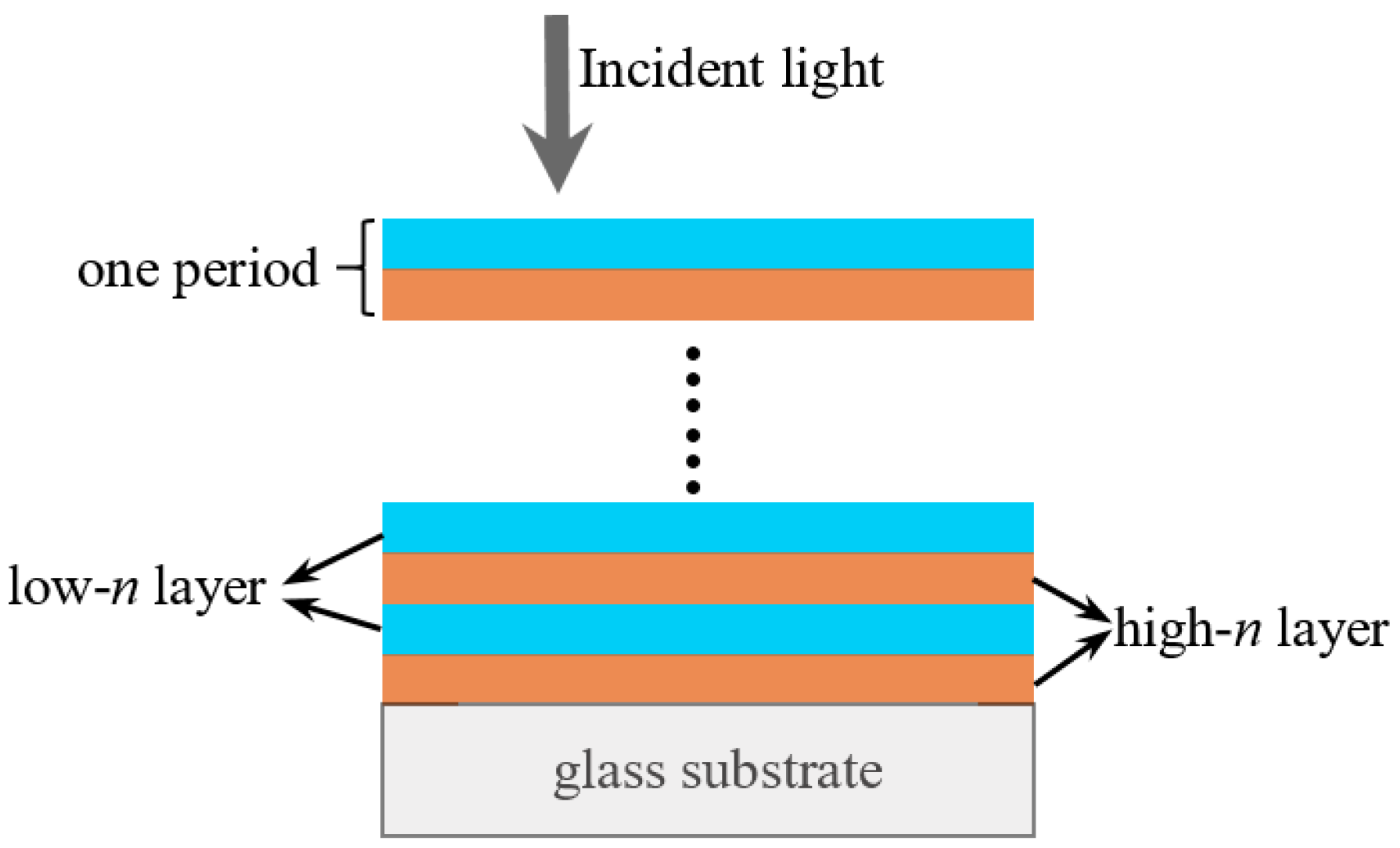
The 1D-PC was formed by periodically stacking of high-n layers and low low-n layers, as shown in Figure 1. In this manuscript, a-Si:H was selected as the high-n layer, while SiO2 was used as the low-n layer because of its transparency, non-dispersion, low refractive index of 1.5 and its compatible deposition process with a-Si:H solar cells [27].
It is difficult to get wide enough PBG to cover the whole absorption range from 300–800 nm for a-Si:H solar cells because of the limited index contrast of the low-n and high-n layers. Therefore, it is crucial to tailor a suitable 1D-PC PBG to match the necessary light-trapping range for a-Si:H solar cells. According to our previous calculation, only light with a wavelength higher than 520 nm can arrive at the bottom of the cell (n-layer) where the back reflection starts to work [27]. As is well known, the upper absorption wavelength limit for a-Si:H is around 750–800 nm corresponding to the bandgap of about 1.6 eV. Therefore, there is little influence of reflected light from the BR outside the wavelength range of 520–800 nm on a-Si:H solar cells’ performance. In conclusion, the PBG should at least cover the range from 520–800 nm to enhance absorption in a-Si:H cells.
2.1.2. Influence of Layer Thickness-Contrast on the PBG
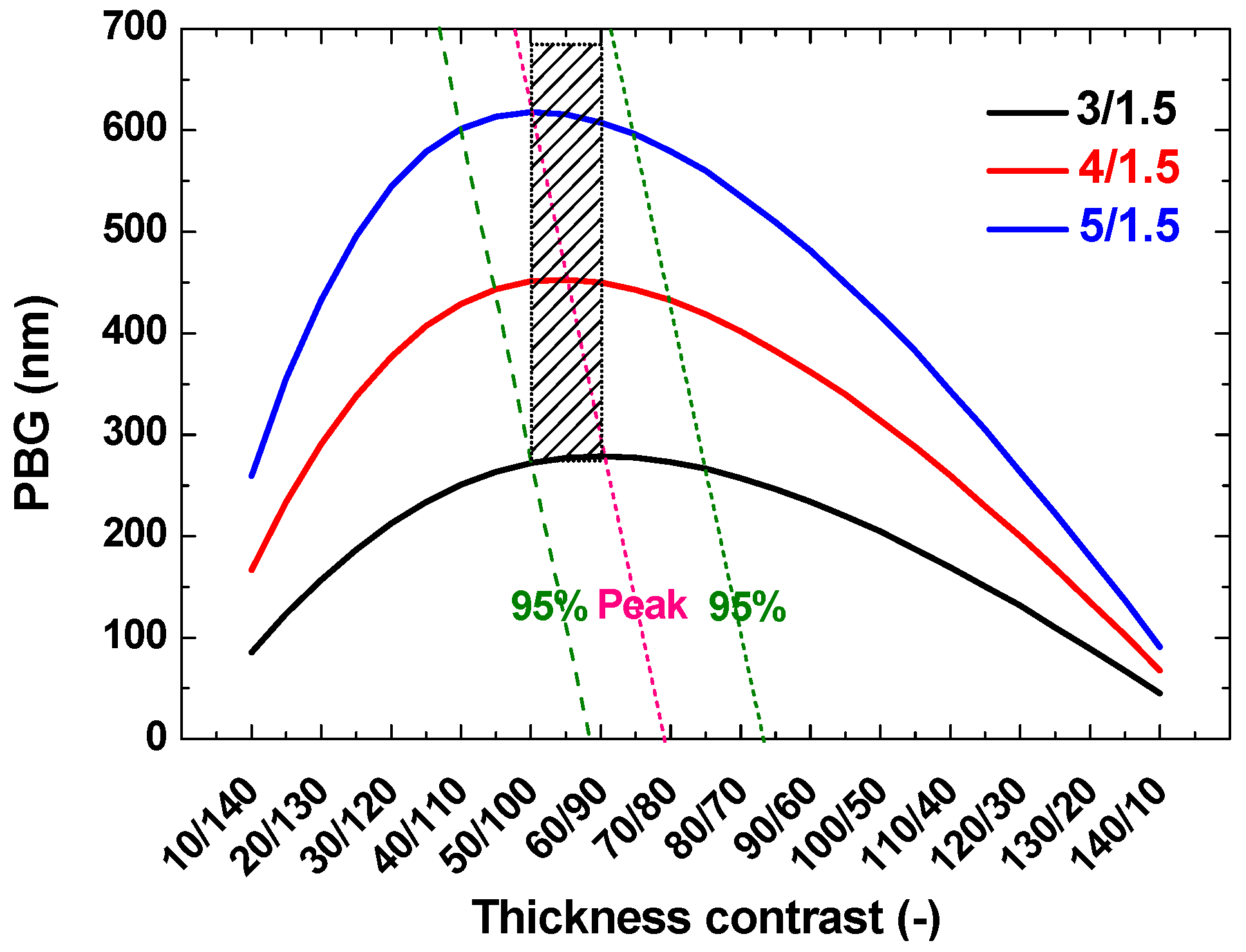
The DBR is one specific kind of 1D-PC, for which the thickness of the individual layer is determined by a quarter-wavelength basis for the Bragg wavelength. When an absorptive layer is inevitably used in 1D-PC or DBR, its thickness should be as thin as possible. Therefore, the performance optimization of the DBR structure is limited. As for a DBR structure, the average reflectivity is closely related to the Bragg wavelength. The periodic thickness and the thickness of the high-n and low-n layer can be calculated using the typical Bragg equation. Figure 2 shows the average reflectivity in the wavelength range of 520–800 nm and the periodic thickness as a function of the Bragg wavelength for the DBR structure with five periods of alternately stacking a high-n layer and a low-n layer. The maximum average reflectivity occurs in the Bragg wavelength (λBragg) range of 600–650 nm, with a corresponding periodic thickness range of 139–152 nm. For comparison, a periodic thickness of 150 nm (λBragg = 640 nm) was employed for PBG simulation. The thicknesses of the a-Si:H (n = 4 at λ = 640 nm) and the SiO2 layers for this optimal DBR structure were 40 nm and 110 nm, respectively.
Figure 3 shows the PBG as a function of thickness-contrast with three different refractive index contrasts (3/1.5, 4/1.5 and 5/1.5). The data of the horizontal axis are the thicknesses of the high-n and low-n layers, while the periodic thickness is 150 nm. For example, the data 10/140 indicate that the thicknesses of the high-n and low-n layers are 10 nm and 140 nm, respectively. Compared with low refractive index contrast, high refractive index contrast would result in a wider PBG, which suggests that the high refractive index contrast of the 1D-PCs is much more beneficial for a-Si:H solar cells. For three refractive index contrasts of 3/1.5, 4/1.5 and 5/1.5, PBGs initially increase followed by slight decreases with the increase of thickness-contrast. Additionally, when increasing the refractive index contrast from 3/1.5–5/1.5, the PBG peak values shift to low thickness-contrast values. It should be noted that the contrast value of 40/110 for the DBR configuration is outside the above-mentioned range from 520–800 nm, which means that DBR is not necessarily the best case in which to achieve the broadest PBG for a certain periodic thickness [27].
2.1.3. Reflection Comparison between DBR and Optimal 1D-PC
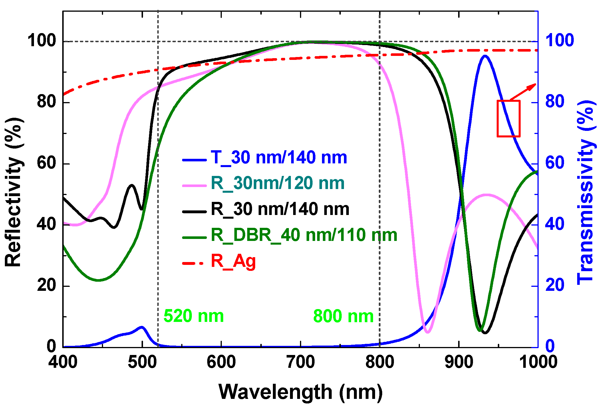
In order to deeply investigate the difference between DBR and 1D-PC, Figure 4 shows simulated reflection spectra of 1D-PC with thickness-contrasts (high-n/low-n layer) 30 nm/120 nm, optimal DBR with thickness-contrasts 40 nm/110 nm and 1D-PC with thickness-contrasts 30 nm/140 nm, respectively. Reference data for the Ag film and the transmission curve for 30 nm/140 nm (T_30 nm/140 nm) are also listed here. Figure 4 showed that the PBG appeared in the wavelength range of 520–800 nm because no transmission was observed from the 1D-PC (T_30 nm/140 nm). A gradual PBG increase was obvious for all thickness-contrast reflection curves. Nearly 100% reflectivity was achieved around 800 nm. A major difference exists in the short wavelength range of 520–620 nm. For the same period thickness of 150 nm, the average reflectivity in the above-mentioned wavelength range decreased with an increase of the thickness-contrast, from 89.3% for 30 nm/120 nm to 84.7% for the DBR structure (40 nm/110 nm), which is lower than that of Ag film 92.2%. However, this reduction can be rather suppressed by increasing the non-absorptive SiO2 layer thickness while retaining the 30-nm absorptive a-Si:H layer. In other words, the thickness-contrast can be decreased further by increasing the period thickness. With a contrast value of 30 nm/140 nm, the 1D-PC yielded an average reflectivity of 96.7% over the whole light-trapping range, and it thus outperformed the 30 nm/120 nm structure with 94.7%, the Ag film with 93.4% and the DBR structure with 93.5%.
2.2. TCPC BRs Formed by 1D-PC and Textured ZnO
It is well known that the essential elements of a highly-efficient back reflector include high reflectivity, high conductivity and strong scattering of the incoming light back into the absorption layer. Previous work usually adopted 2D gratings on the TCO layer [30] or even on the 1D-PC to introduce scattering into 1D-PC with TCO. Although simulation results show a significant improvement of optical absorption compared with the flat one, the current experimental results were not so satisfactory [11,23]. As a matter of fact, the steep valleys of the gratings would inevitably result in micro voids within the absorption layers and then cause deterioration of the device performance [32]. Some other groups suggest depositing 1D-PC on a textured substrate (random [16] or periodic grating [23]). However, conformal growth usually is difficult between periodic layers for multi-layered structures, especially on highly-textured substrates. Thus, the periodic symmetry of 1D-PC would be destroyed, resulting in a reduction of reflectivity and an offset of the reflection region.
2.2.1. Design and Fabrication
Here, we developed a texture conductive photonic crystal (TCPC) BR to improve the performance of the n-i-p a-Si:H solar cells. The first step was to deposit 1D-PC on a flat glass, and the following process was to sputter a thick AZO film (800 nm) with a lower sheet resistance (Rsq) of 5 Ω/sq. After that, the whole sample was chemically etched in 0.5% hydrochloric acid to introduce a randomly-textured surface, which led to a slight increase of Rsq to 10 Ω/sq. The 1D-PC structure is alternatively stacked with a 155-nm SiOx upper layer and a 25-nm a-Si:H under layer with five periods. Figure 5 shows the schematic diagram of the TCPC BR-based n-i-p a-Si:H solar cell. Since the 1D-PC structure is dielectric and non-conducting, a highly-conductive TCO layer is specifically needed for the TCPC- and CPC-based cells.
Focus was placed on n-i-p a-Si:H solar cells with the structure of BR/n-a-Si:H (15 nm)/i-a-Si:H (300 nm)/p-nc-Si:H (15 nm)/ITO (70 nm) as a convenient prototype. All of the p, i, n layers, as well as 1D-PC were deposited in a multi-chamber RF-PECVD system. The AZO film was deposited using a radio-frequency sputtering system with a ceramic ZnO target with 2 wt % Al2O3. For comparison, a reference AZO (100 nm)/textured Ag BR was fabricated by the same sputtering system.
2.2.2. Structural Properties
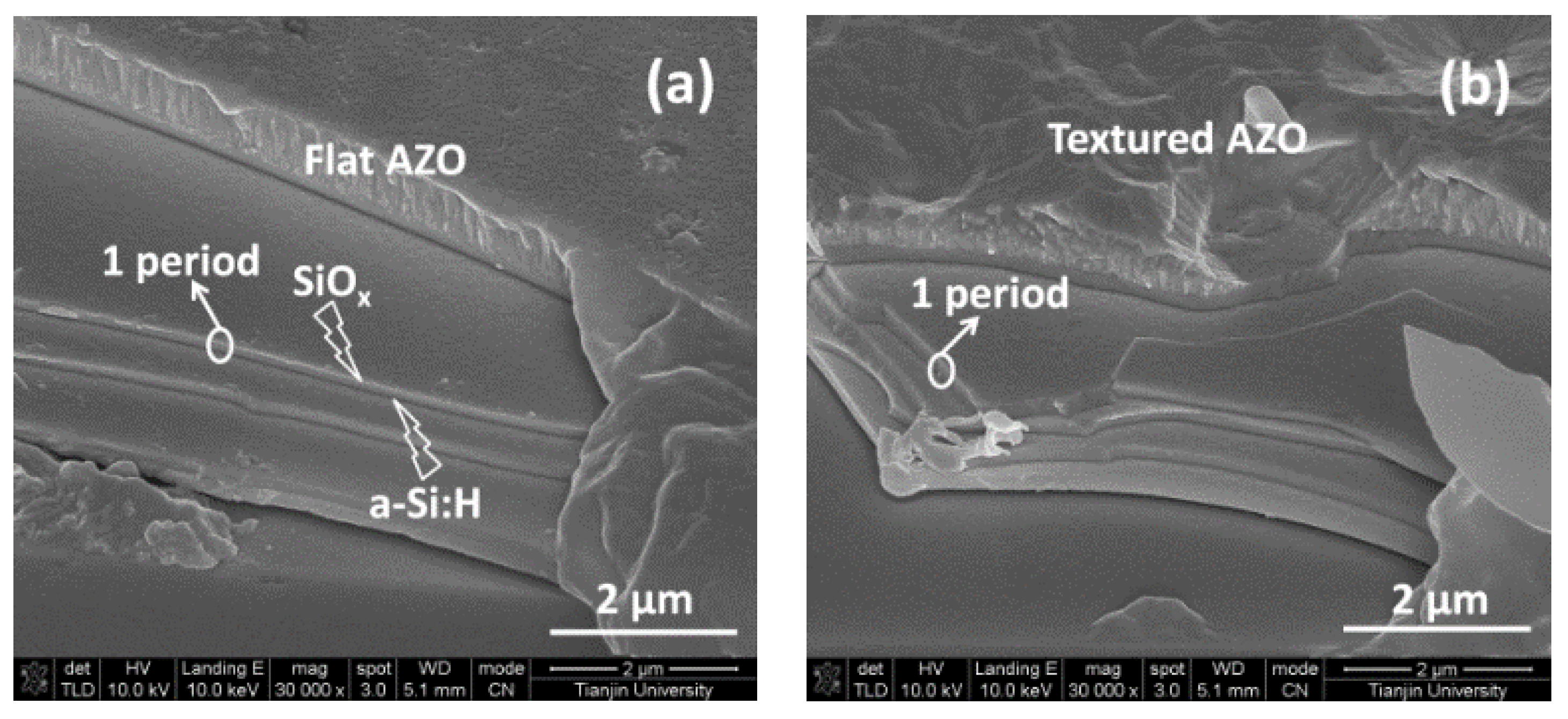
Figure 6 shows the cross-sectional SEM images of CPC and TCPC BRs, respectively. It is obviously found that five periods of flat 1D-PC were deposited, and the surface morphology was changed from flat to textured by chemical etching of CPC. Usually, textured surfaces with relatively large features demonstrate high haze factors and then a better light-trapping effect [39]. An root mean square (RMS) value of 126 nm was obtained for our TCPC with a crater-like surface, as can be seen from the AFM images of Figure 7a. In traditional n-i-p thin-film silicon solar cells, textured Ag/AZO(100–150 nm) BRs were proven to be efficient light-trapping structures and produced the best cell performance by United Solar before [15,40]. It is noteworthy that highly textured Ag interfaces inevitably lead to not only plasmonic loss, but also other defect-induced loss in narrow angle valleys, thus to counteract the gain from enhanced scattering. Yan et al. achieved a short-circuit current over 30 mA/cm2 in nc-Si:H solar cells based on an optimized textured AZO/Ag BR with an RMS value of ~40 nm and a lateral feature size of ~500 nm [15]. The RMS value (39 nm) and lateral feature size of the reference AZO/Ag BR, as shown in Figure 7b, are similar to those in the literature [15], as illustrated in Figure 7b. With respect to Ag/AZO, a more moderate surface morphology can be observed for TCPC, which is hopeful to offer a favorable physical property for the growth of TFSC [32,41].
2.2.3. Optical Properties
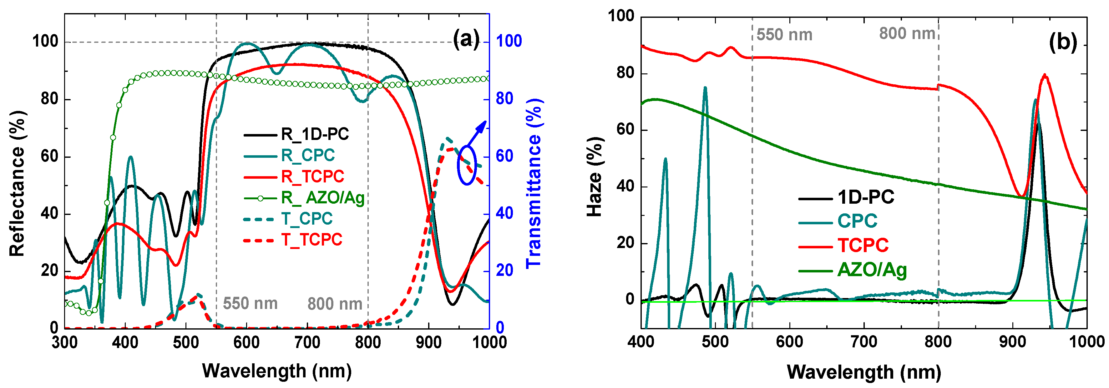
Figure 8 shows the total reflectance (TR), transmittance (TT) and haze factors of various BRs including TCPC, flat 1D-PC, CPC and textured AZO/Ag. It can be observed that interference fringes occurred if thick AZO films were incorporated into 1D-PC to form CPC. Thus, the average TR decreased from 98% down to 92.4% in the wavelength range of 550–800 nm. However, the interference fringes disappear after chemical etching due to the diffuse reflection caused by the rough surface. An average TR of 90.4% can be obtained for TCPC, which is much better than AZO/Ag with TR of 85.8%. Nearly no transmission can be observed in the wavelength range of 550–800 nm whether a chemical etching process is applied or not. Previous work showed that the incident light only couples into the top three periods of 1D-PC [27]. Because the rough interface would lead to angled incidence, which elongates the optical path length in the AZO layer and 1D-PC, the TR decrease from CPC to TCPC is mainly afforded by both the increase of free carrier absorption of AZO layers and enhanced bulk absorption of 1D-PC. In fact, the TR would even be reinforced in actual devices, because it will be easier to form total internal reflection at the rough a-Si:H/AZO interface. A much higher average haze factor of 80.6% in the light-trapping range (550–800 nm) can be obtained for TCPC, corresponding to a relative enhancement of 69% compared to the AZO/Ag (47.8%).
2.2.4. TCPC BRs for a-Si:H Solar Cells
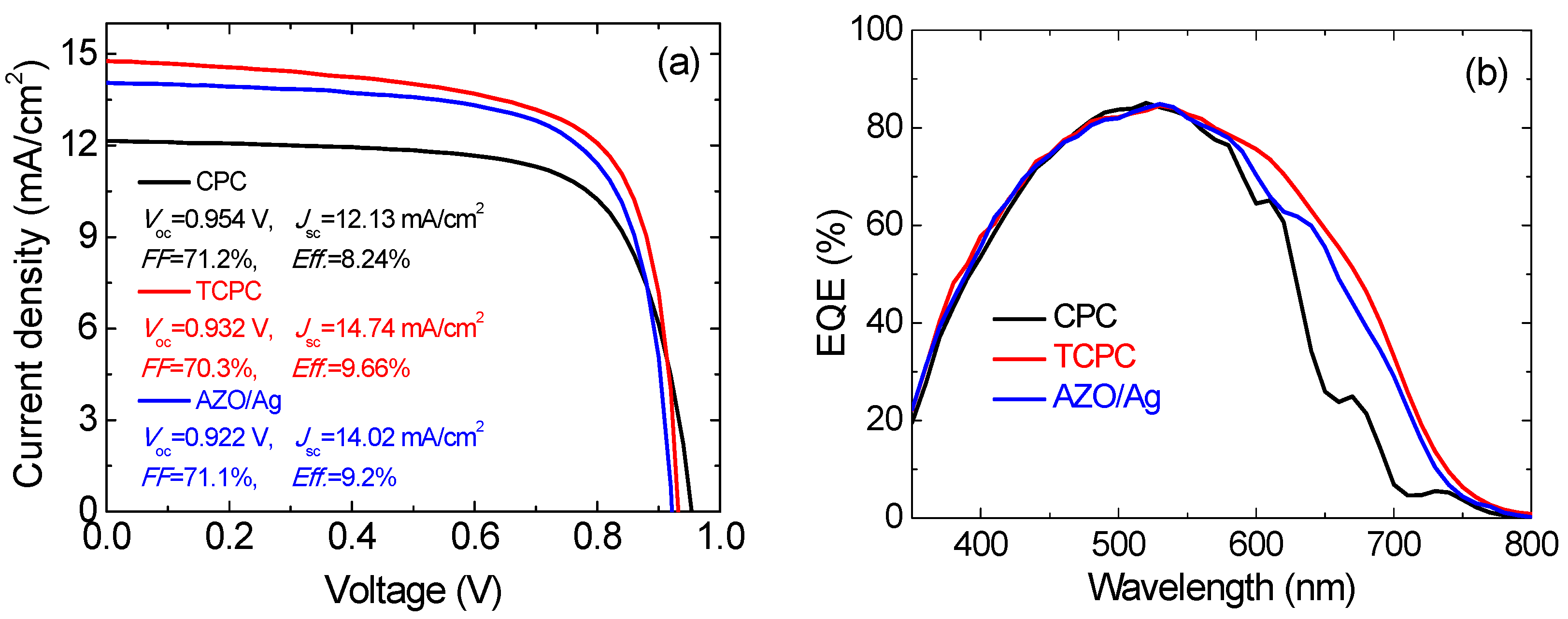
The above-mentioned CPC, TCPC and AZO/Ag BRs were applied to n-i-p a-Si:H solar cells to further investigate their influence on solar cell performance. J–V and external quantum efficiency (EQE) curves of a-Si:H solar cells are shown in Figure 9a,b, respectively. Slight decreases of Voc can be seen for TCPC-based and AZO/Ag-based solar cells, which were mainly caused by the textured interface [42]. Compared to the highly conductive AZO/Ag-based and the flat CPC-based solar cells, no significant deterioration of fill factor (FF) can be observed for the TCPC-based cell. This indicates that the TCPC BR can simultaneously serve as a sufficient electrical contact and provide a moderately textured surface, which is beneficial to reduce micro-void defects. EQE values in the wavelength range of 550–800 nm were significantly improved by introducing textured morphology for AZO/Ag- and TCPC-based solar cell BRs, while obvious interference fringes were observed in the flat CPC-based solar cell. For the CPC-based solar cell, the Jsc is 12.13 mA/cm2, while it is 14.74 mA/cm2 for the TCPC-based solar cell. The conversion efficiency increases from 8.24% for CPC BR to 9.66% for TCPC BR, corresponding to a relative enhancement of 17.2%. Additionally, an enhancement of 5% for both Jsc and efficiency was obtained for the TCPC-based solar cell, compared to the AZO/Ag-based solar cell (Jsc = 14.02 mA/cm2, efficiency (Eff.) = 9.2%).
2.3. RTPC BRs Formed by Textured ZnO and Textured 1D-PC
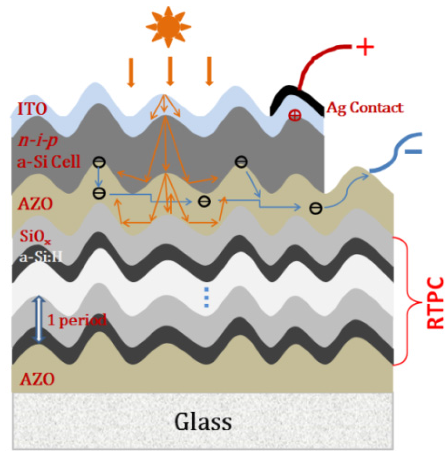
In this section, a novel randomly-textured photonic crystal (RTPC) BR was developed to improve light-trapping and then solar cell performance by stacking a 1D-PC onto a randomly-textured AZO template.
2.3.1. Design, Fabrication and Simulation
Figure 10 shows the schematic diagram of an n-i-p a-Si:H solar cell with an RTPC BR. A thick AZO film (1.5 μm) was firstly deposited on a flat glass using a radio-frequency (RF) magnetron sputtering system. After that, the AZO film was chemically etched in 0.5% HCl to create a textured surface. Then, 1D-PC formed by periodic stacking of a-Si:H and SiOx was deposited to form the RTPC. Since the a-Si:H is absorptive, the bulk absorption of RTPC still occurs. Here, a very thin a-Si:H layer (25 nm) was used to reduce the bulk absorption while maintaining the PBG in the light-trapping range from 520–800 nm. Therefore, the 1D-PC or RTPC structures consist of 155 nm SiOx as the upper layers and 25 nm a-Si:H as the under layers.
A highly conductive AZO film with sheet resistance of ~10 Ω/sq and thickness of 400 nm was inserted between the RTPC and a-Si:H layers as an electrical contact. Since the RTPC is nonconductive, the electrical current flows laterally in the AZO layer and is collected by the metal cathode. The complete structure of the n-i-p a-Si:H solar cell was BR/n-a-Si:H (15 nm)/i-a-Si:H (300 nm)/p-nc-Si:H (15 nm)/ITO (80 nm). The p, i, and n layers, as well as the RTPC were deposited using the same multi-chamber radio frequency plasma enhanced chemical vapor deposition (RF-PECVD) system.
2.3.2. Surface Morphology
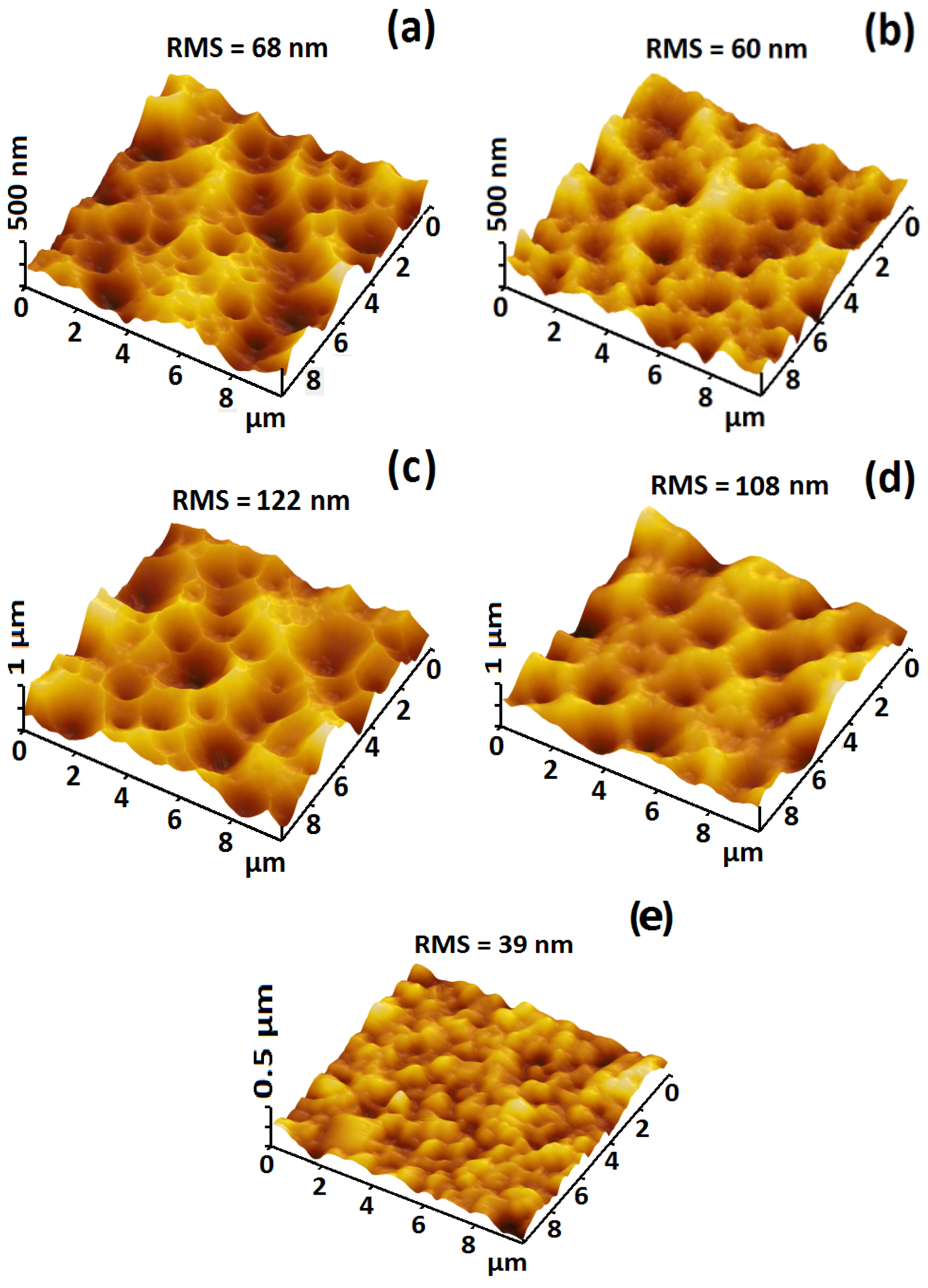
The RTPC1 with medium-sized texture and the RTPC2 with large texture were prepared to study the effect of different roughness on the optical properties of RTPCs. Figure 11 shows AFM images of AZO1, RTPC1 on AZO1, AZO2, RTPC2 on AZO2 and randomly-textured AZO/Ag. It is obvious that thicker RTPCs (~900 nm) make the surface texture tend to be smooth. For example, the RMS value of the AZO1 in Figure 11a is 68 nm, while it decreases to 60 nm in Figure 11b after RTPC1 deposition. AZO2 and corresponding RTPC2 have a similar tendency, as shown in Figure 11c,d. A very smooth surface was obtained with the deposition of RTPC, which might offer favorable surface texture to realize conformal growth of silicon layers.
2.3.3. Optical Properties
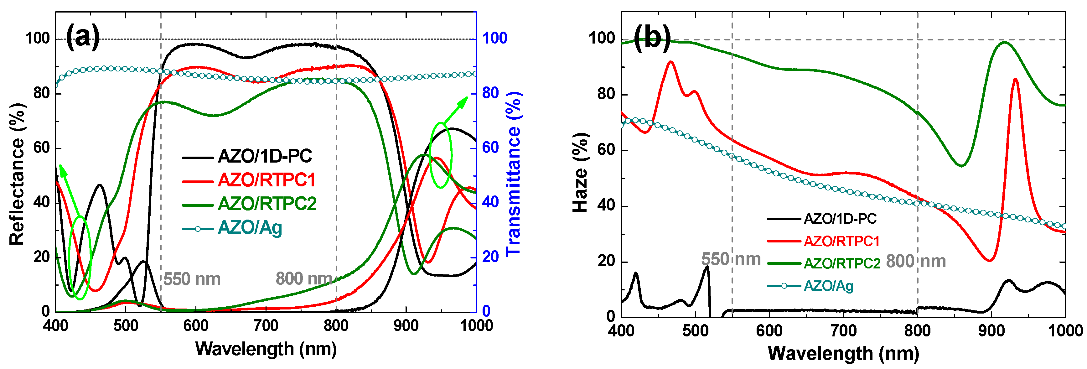
The total reflectance (TR), transmittance (TT) and haze factor of flat 1D-PC, RTPC1 and RTPC2 are shown in Figure 12a,b, respectively. TR values are 98%, 91% and 87% for the 1D-PC, RTPC1 and RTPC2, respectively. With the increase of RMS roughness, the TR in the light-trapping range from 550–800 nm decreases step-by-step, while the haze factor significantly increases continuously. These phenomena can be explained by the oblique incidence on the rough surface, which then leads to a longer path of light propagation. That is to say, the enhanced RTPC absorption leads to the TR reduction, especially in the wavelength range from 550–650 nm, in which the a-Si:H layer has a high absorption coefficient [35]. Our previous work showed that for the flat 1D-PC, sunlight was only coupled into the top three pairs of layers [27]. As for RTPC, the situation is somewhat different from flat 1D-PC. In the range from 650–800 nm, both the bulk absorption of RTPC, parasitic absorption of the AZO template and optical losses caused the TR reduction.
Figure 13 shows the optical properties of RTPCs with AZO (400 nm). The results for AZO (400 nm)/flat 1D-PC and randomly-textured AZO (100 nm)/Ag were plotted as references. The results showed that RTPC1 has both higher TR and haze than the textured AZO/Ag. Although RTPC2 has the highest haze, its TR is the lowest. It should be mentioned that the RTPC texture is transferred to the AZO surface, and light scatters from both the air/AZO and AZO/RTPC interfaces. Since AZO has a higher refractive index than air, much more light should be trapped within the highly textured AZO layer, which inevitably results in greater optical loss in the BR. Because of the quarter-wavelength antireflection effect of the AZO layer, reflection valleys were observed in the PBG area for the AZO-based 1D-PC and RTPCs. In the meantime, due to the unequal growth rate of AZO deposited on RTPCs with different roughnesses, the reflection valley shifts slightly [43].
2.3.4. RTPC BRs for a-Si:H Solar Cells
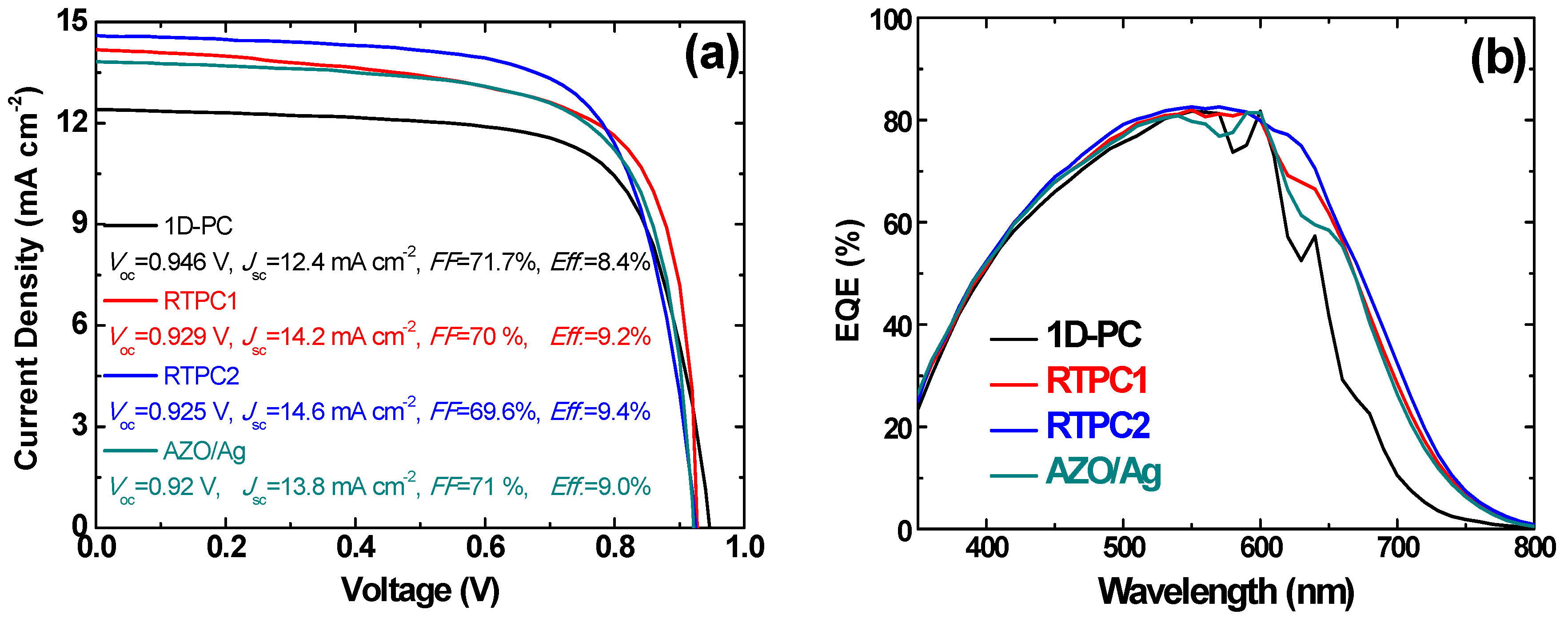
Next AZO/1D-PC, AZO/RTPC1, AZO/RTPC2 and randomly-textured AZO/Ag BRs were applied to n-i-p a-Si:H solar cells. Corresponding J–V and EQE curves of these a-Si:H solar cells are shown in Figure 14. Slight decreases of Voc are found for those solar cells with textured BRs. All solar cells demonstrate similar FF, which indicates that the AZO/RTPC can simultaneously serve as an efficient electrical contact and provide moderately-textured surfaces. This is beneficial to reduce the defect densities between BRs and silicon layers.
The EQE values in the wavelength range from 550–800 nm are obviously improved for AZO/RTPC1, AZO/RTPC2 and AZO/Ag BR-based solar cells with textured surfaces. With the increase of roughness, the interference fringes caused by directly reflection drop gradually. Because of its higher TR and haze, the EQE is enhanced for the AZO/RTPC1-based solar cell with respect to the textured AZO/Ag-based solar cell. Although AZO/RTPC2 BR provides the lowest TR for incidence from air, the corresponding solar cell still offers the highest EQE values. Since there is a π-phase shift at the air/AZO interface and the a-Si:H/AZO interface [10], the interference-induced reduction of TR at air/AZO interface reverses and becomes a TR enhancement at a-Si:H/AZO interface. Therefore, the Jsc of the solar cell increases. Furthermore, the light trapped within the AZO will also emerge in the a-Si:H solar cell because total internal reflection occurs more easily because of the reduced index matching at the a-Si:H/AZO interface. Thus, the reduced reflection of AZO/RTPC2 measured in air may not consequently cause a Jsc reduction. In this case, the increased scattering might dominate light-trapping in solar cells, as shown in Figure 14b.
The calculated Jsc for the AZO/1D-PC-based solar cell and the AZO/RTPC2-based cell are 12.4 mA/cm2 and 14.6 mA/cm2, respectively. Initial efficiencies for these two solar cells are 8.4%–9.4%, corresponding to a relative enhancement of 12%. Furthermore, for the AZO/RTPC2-based solar cell, a relative Jsc enhancement of 5.8% and a relative efficiency enhancement of 4.5% can be obtained with respect to the AZO/Ag-based solar cell.
3. 2D-PC Back Reflectors and Applications
In this section, two novel BRs, micro-cone patterned substrates (MCPSs) and quasi-photonic crystal structures (QCS), were developed to improve both light coupling and the light-trapping effect for n-i-p silicon thin film solar cells. The waviness of the BRs’ profiles were copied to the following deposited thin film layers, thus to fulfill two critical criteria in solar energy harvesting by (i) the gradient index profile for antireflection and (ii) the elongating optical path length for enhanced absorption. Focus was placed on the n-i-p a-SiGe:H solar cell due to its broader absorption wavelength range [44] than the a-Si:H solar cell and thinner absorbing layer than the μc-Si:H solar cell. This would be more conductive to reveal the light harvesting mechanism of the micro-cone textures.
3.1. Periodically Patterned Micro-Cone Texture BRs
3.1.1. Preparation of MCPS BRs and Solar Cells
A well-known thermally-reflowed photoresist and dry etching method were used to fabricate MCPS [45,46] by the following process. An array of circular photo resist patterns was fabricated first on c-oriented sapphires by standard photolithography technology. The wafers were then baked out on a hot plate at different temperatures as the thermal photo resist reflow method. The inductive coupled plasma dry etching process was performed on these convex-patterned sapphire substrates. With different reflow temperatures, different pattern shapes can be fabricated on the sapphire substrate surface after the inductively-coupled plasma etching process.
Ag/ZnO:Al (AZO) stacked film (100 nm/100 nm) was deposited on the MCPS by sputtering at room temperature to obtain a micro-rough, but nano-flat surface of MCPS/Ag/AZO BR. Flat and randomly nanotextured Ag/AZO BRs were deposited as references. The solar cell structure consists of BR/n-a-Si:H (15 nm)/i-a-SiGe:H (200 nm)/p-nc-Si:H (15 nm)/ITO (80 nm).
3.1.2. Structural Properties
A uniform micro-cone pattern, shown in Figure 15a, was reproducibly obtained using the above fabrication procedure. The lateral period of all MCPSs was fixed at 3 μm (P = 3 μm), which is much larger than the total thickness of an a-SiGe:H solar cell (~0.5 μm). The diameter of each cone-shaped pattern was fixed at 2.6, and thus, the interval between neighboring cone-shaped patterns was 0.4 μm, as illustrated in Figure 15b. Therefore, a quasi-U-shape was formed, which is beneficial for the growth of high-quality silicon layers. We define the aspect ratio of such patterns as the ratio of height to the lateral period, namely H/P. Figure 15c–e shows the cross-sectional SEM images of MCPSs with three different heights of 0.5, 1.0 and 1.5 μm, with the same lateral period of 3 μm. We denoted these substrates as P3H0.5, P3H1.0 and P3H1.5, respectively.
Figure 16 shows the SEM images of three MCPS, MCPS coated with Ag/AZO and corresponding solar cells. All three MCPSs showed uniform patterns regardless of the heights. The surface morphologies of MCPSs were well maintained after the deposition of each layer. Ag/AZO layers were deposited at room temperature on the MCPSs. In this case, relatively smooth surfaces can be achieved at the sub-micro scale, which resulted in a conformal growth.
3.1.3. Optical Properties
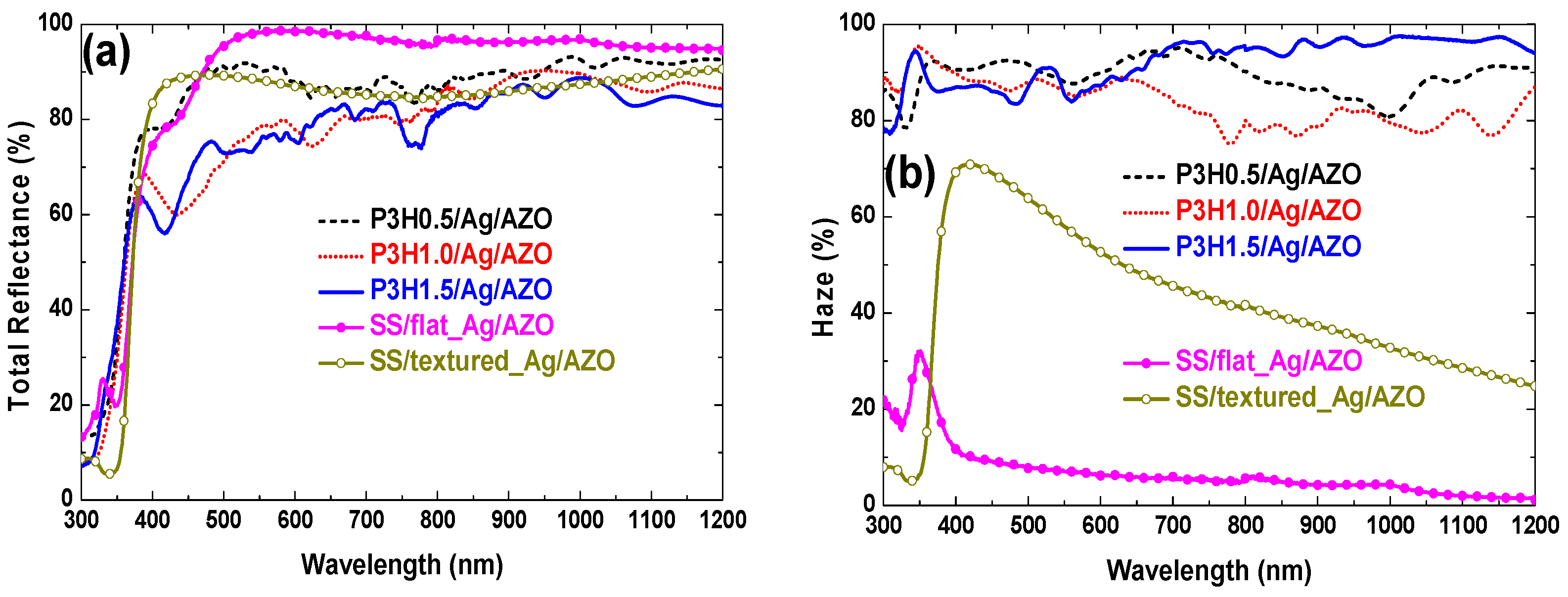
Light-trapping capacity strongly depends on the reflecting and scattering ability of BRs [15,48]. Figure 17 demonstrates the optical properties of three MCPS BRs (P3H0.5/Ag/AZO, P3H1/Ag/AZO, P3H1.5/Ag/AZO), where the total reflectance and haze factor are shown in Figure 17a,b, respectively. The results of flat Ag/AZO (SS/flat_Ag/AZO) and randomly nanotextured Ag/AZO (SS/textured_Ag/AZO, RMS of 39 nm and lateral feature size from 100 nm to 500 nm) on stainless steel foils (SS) are plotted as references. Compared with the flat BR, a TR reduction appeared for textured BRs (random or micro-cone) because of intrinsic losses caused by the surface plasmon absorption of the silver layer [49]. Although the RMS of P3H0.5/Ag/AZO is much higher than that of randomly nanotextured BR, they demonstrate similar TR. Further increasing the aspect ratio to 1/3 or 1/2 lead to a TR decrease in the wavelength range of 400–900 nm, indicating that the surface plasmon absorption increased with the aspect ratio in this wavelength region. All MCPS BRs have high a haze factor of around 90% across the whole wavelength range. According to the traditional light-trapping theory, a significant absorption enhancement in the near-IR region is expectable [15,35]. The best solar cell performance seems to be achieved by the P3H0.5 BR due to its higher reflectivity, higher haze factor and moderate substrate morphology. Unlike the smooth reflection curve for the randomly nanotextured BR, many ripples appeared for MCPS BRs in the whole wavelength range from 400–1200 nm, corresponding to a series of diffraction governed by the so-called grating equation [23]. This suggests that waveguide modes still exist when applying micro-cone BRs to the solar cells.
3.1.4. MCPS BRs for a-SiGe:H Solar Cells
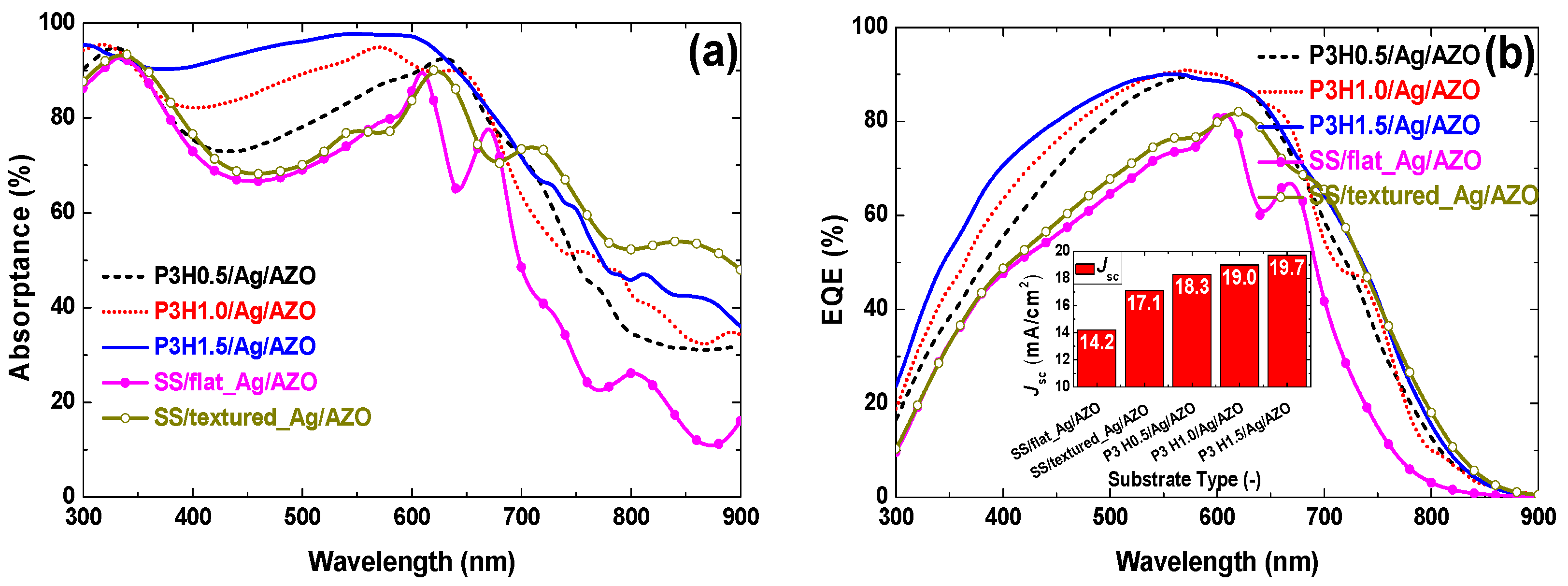
The above-mentioned P3H0.5/Ag/AZO, P3H1.0/Ag/AZO, P3H1.5/Ag/AZO, SS/flat_Ag/AZO and SS/textured_Ag/AZO BRs were incorporated into n-i-p a-SiGe:H solar cells to further study the influence of the electrical and optical properties of BRs on the solar-cell performance. The corresponding total absorptance (1−R) and EQE of the above a-SiGe:H solar cells are shown in Figure 18a,b, respectively.
Figure 18 shows that both the total absorptance and EQE were substantially improved in the wavelength range from 300–600 nm for MCPS BRs with respect to the flat (SS/flat_Ag/AZO) and randomly nanotextured (SS/textured_Ag/AZO) references. Compared with the flat reference sample, the average absorption and EQE value of P3H1.5 MCPS BR in the above short wavelength range can be improved by a relative enhancement of 23% and 37.5%, respectively. Due to the high absorption coefficient of a-SiGe:H in this wavelength range, the light coupled in the solar cells is almost completely absorbed within one optical path length. Nearly no light goes through the whole solar cell and arrives at the backside. Thus, the difference between the absorption and EQE values among these solar cells in the short wavelength region was mainly caused by different antireflection effects of the front surfaces. For the solar cell with randomly nanotextured BR, the nanotextured profile tends to be flattened with the increase of thickness during the film deposition, and then, a relatively smooth front surface formed. In this case, the antireflection effect was fully dependent on the ITO antireflection coating.
For MCPS BR-based solar cells, the micro-cone front surfaces result in a gradually changed refractive index at the air/ITO interface according to the effective medium theory [50,51,52]. In the wavelength range of 300–600 nm the MCPS BR-based solar cells exhibited higher absorption than the flat and randomly nanotextured samples thanks to the double excellent antireflection effect originating from the (i) anti-reflective coating and (ii) gradient index profile. The total absorptance and EQE values in the short wavelength range from 300–600 nm increase with the increase of the aspect ratio. This can contribute to a smoother change of index profile generated by a higher aspect ratio and an increased probability for the incident light. In the long wavelength range from 600–900 nm, the total absorptance and EQE for MCPS-based solar cells was also significantly improved with respect to the flat one, as shown in Figure 18a,b. A reduction of reflection could be also achieved in the long wavelength range according to the above description. Light absorption enhancement obtained by enhanced light-trapping via the micro-cone textured BR plays a more crucial role than enhanced light coupling from the front surface, especially in the IR or near-IR region.
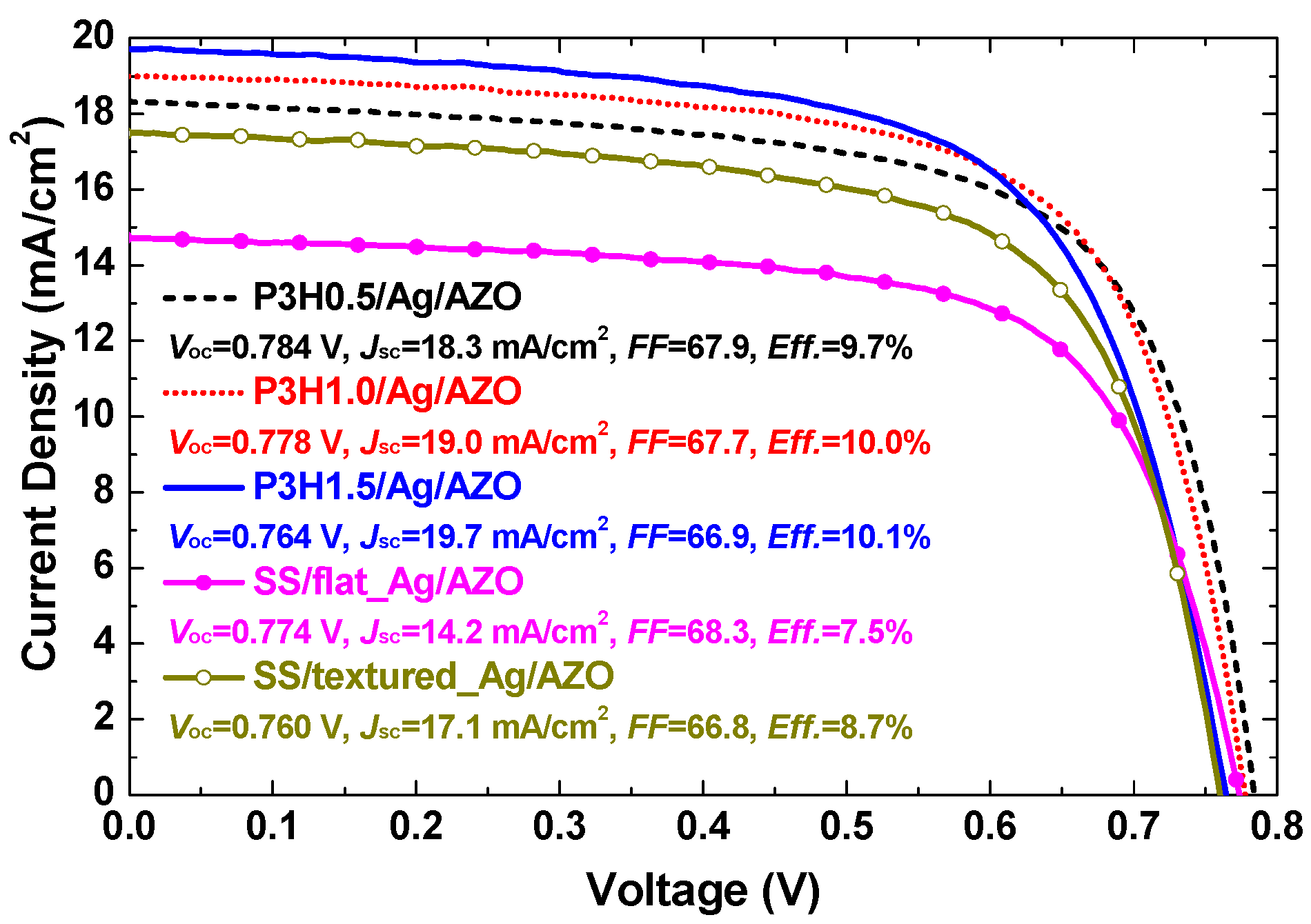
Because of their light coupling and light-trapping capacity, the MCPS BRs are promising candidates as substrates to realize high conversion efficiency. J–V curves of a-SiGe:H solar cells with different BRs (P3H0.5/Ag/AZO, P3H1.0/Ag/AZO, P3H1.5/Ag/AZO, SS/flat_Ag/AZO, SS/textured_Ag/AZO) are shown in Figure 19. The Voc and FF of MCPS-based solar cells are almost as high as the flat cell, indicating sufficiently smooth surfaces of micro-cone textures and much lower texture-induced crack defects. For the flat solar cell and the MCPS-based solar cell with the aspect ratio of 0.5 (P3H1.5), the Jsc are14.2 mA/cm2 and 19.7 mA/cm2, respectively, corresponding to a relative increase of 38.7%. The solar cell efficiencies are 7.5% and 10.1%, respectively, corresponding to a relative increase of 34.7%. In addition, the respective Jsc and efficiency enhancement of 15.2% and 16.1% are achieved with respect to the randomly nanotextured BR solar cell. For three MCPS-based solar cells the Voc and FF slightly deceased with the increase of the aspect ratio, which can probably contribute to the defects caused by the sharper peaks and narrower valleys of micro-cones. By moderating the peaks and valleys of micro-cones, further efficiency enhancement is expectable for the MCPS-based solar cells with a higher aspect ratio.
Although the haze factor of SS/textured_Ag/AZO BR is significantly lower than MCPS BRs, it offers a slightly better IR or near-IR spectral response than the latter ones, as shown in Figure 18b. These results clearly demonstrate that diffuse reflectivity (or haze) is not the only indicator of light-trapping ability. As everyone knows, a high diffraction order with a large diffraction angle could diffract incoming light into highly oblique angles, which is beneficial for an elongating optical path length to improve light absorption. Therefore, great effort should be targeted at how to enhance the diffraction efficiency of high diffraction to efficiently improve the light-trapping ability of periodic BRs. However, the diffraction efficiency distributed for high diffraction orders is not so much for a periodic microscale structure due to its large amounts of diffraction orders. The situation is somewhat different for a periodic nanotextured structure since only a few diffraction orders can be obtained according to the grating equation. If both the periodic nanoscale and microscale structures have the same total diffraction efficiency, the nanoscale structures can provide higher diffraction efficiency at the high diffraction order than the microscale ones due to its lower number of diffraction orders. It is assumed that the randomly nanotextured surface can be approximated by the superposition of periodically sinusoidal/cosinusoidal nanotextured surfaces, which represent the Fourier decomposition of the surface [53]. In this case, a series of continuous diffraction peaks can be observed at each diffraction order for the randomly nanotextured BR, finally resulting in a smooth EQE curve in the relative solar cells. Since there are only a few diffraction orders for the randomly nanotextured structures, the diffraction peaks could be overall stronger than the periodic microtextured ones at the high diffraction order, thus resulting in an improved spectral response.
The above-mentioned results demonstrated that both light coupling and light-trapping contribute to the absorption enhancement of MCPS BR-based solar cells in the long wavelength range. Without a doubt, light-trapping plays a more crucial role. To maximally improve the light coupling via the micro-cone pattern, the incident light should be absorbed in solar cells without escaping from the surface. That is to say that the formula αd ≥ 1 should be satisfied, where α and d is the absorption coefficient and the optical path length in solar cells, respectively. This is easier to realize for short wavelength light due to its high α. If such a condition is also satisfied for long wavelength light, the absorptance should be as close to 100% as possible. However, it is scarcely possible for silicon film to get such high absorptance for long wavelength light. This indicates that light coupling improvement via micro-cone structures can become more effective when the optical path length within the device becomes longer by thickening the solar cell and/or further improving the light-trapping effect, such as introducing the nanotextured surface into the micro-cone BR to realize a micro-/nano-hybrid texture.
3.2. Quasi-Crystal Structures Formed by 2D-PC and Textured Ag/ZnO
3.2.1. Experiments
Periodic arrays of micro-cone textures were achieved by patterning sapphire substrates (PSS) [54] using a well-known thermally-reflowed photoresist and dry etching method in the light-emitting diode (LED) industry [44,45], as described in Section 3.1.1. Micro-cone textured P3H1.5 PSS, as shown in Figure 15 and described in Section 3.1.2, was used in this section with a fixed lateral period of 3 μm, a fixed height of 1.5 μm and thus a constant aspect ratio (H/P) of 0.5. When deposited at room temperature, the Ag layer surface was relatively flat. If a flat Ag layer were deposited on the P3H1.5 PSS, a micro-cone structure (MCS) was formed. In this case, the waviness of P3H1.5 PSS was well retained after the flat Ag layer deposition. When a randomly nanotextured Ag layer was sputtered on a P3H1.5 PSS, a quasi-crystal structure (QCS) was obtained. The feature sizes of randomly nanotextured Ag layers were controlled by changing substrate temperatures and film thicknesses. In order to suppress the parasitic plasmon absorption generated on the rough Ag surface, the 100-nm AZO layer was deposited on the Ag layers. The structure of n-i-p a-SiGe:H solar cells consists of BR/n-a-Si:H (15 nm)/i-a-SiGe:H(200 nm)/p-nc-Si:H (15 nm)/ITO (80 nm).
3.2.2. Surface Morphology
Figure 20 shows SEM images of QCS, MCS and a-SiGe:H solar cells on these two substrates. Here, the RMS value of the randomly nanotextured Ag is about 40 nm as measured by AFM, with the lateral feature size ranging from a hundred nanometers to sub-micrometer. The morphologies of the MCS and QCS are quite different from each other. The MCS has a nano-flat surface like that of the P3H1.5 PSS, while the QCS looks like neatly arranged flowers with a random nano-textured surface. Encouragingly, it is found that the peaks of P3H1.5 PSS become moderate after the deposition of the Ag layer regardless of being textured or flat, indicating that the leakage current caused by the sharp peaks can be prohibited for both QCS-based and MCS-based solar cells. In addition, the surfaces of the QCS-based and MCS-based solar cells are similar to each other, implying that the randomly nanotextured surface of the QCS has been largely flattened after the solar cell deposition. Hence, we assumed that QCS-based and MCS-based solar cells have an approximated anti-reflection effect due to their similar surfaces, especially for short wavelength light for which the absorptions are largely dependent on the front-surface reflection.
3.2.3. Optical Properties
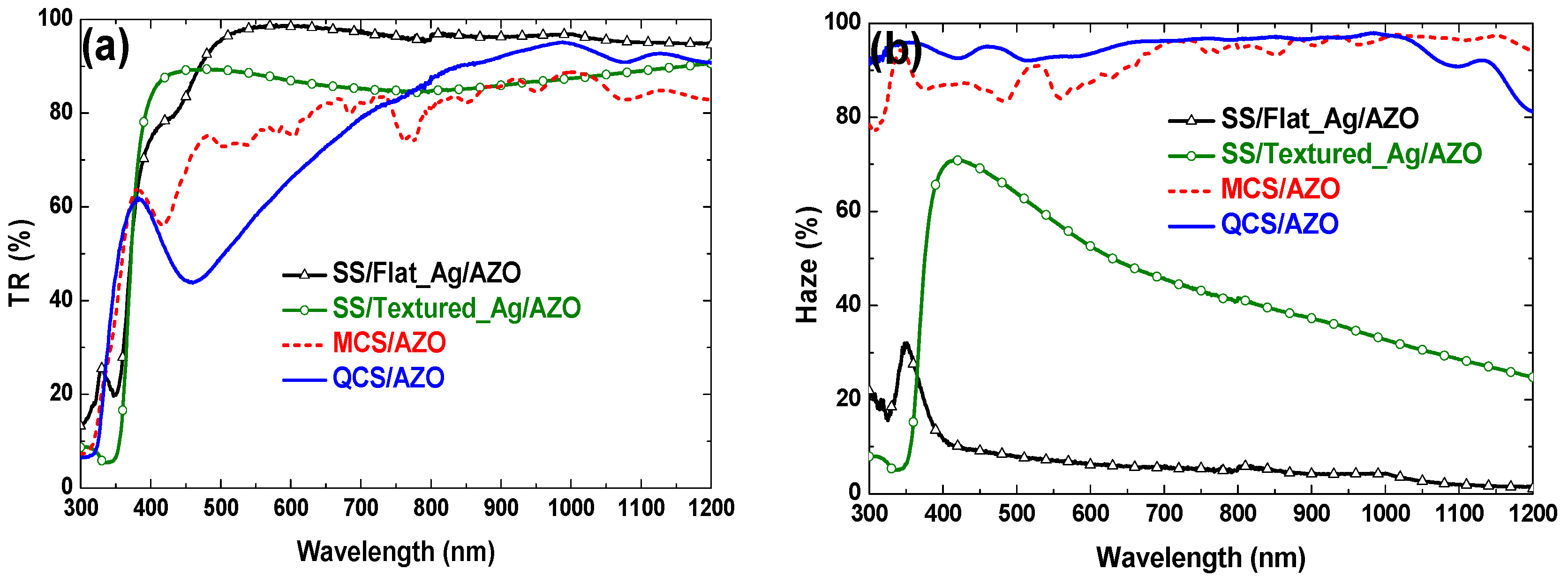
Figure 21 shows the total reflection and haze factor of QCS/AZO and MCS/AZO BRs. The results of flat Ag/AZO and randomly nanotextured Ag/AZO using the same sputtering parameters as MCS/AZO and QCS/AZO, respectively, were also plotted as references. It is clear that the introduction of textured Ag layers, irrespective of random or periodic, micro or nano, would inevitably results in extra surface plasmon absorptions [48] even covered with AZO layers. Unlike the smooth reflection curve of the SS/textured_Ag/AZO BR, many ripples appear on the spectra of the MCS/AZO, which correspond to a series of diffraction governed by the grating equation [23]. For the QCS/ZnO BR, the diffraction peaks disappear, indicating that periodicity has been disrupted. For the short wavelength light, plasmon absorptions of textured BRs increase with the increase of roughness (from randomly nanotextured to micro-cone textured to quasi-crystal textured). However, this tendency disappears for long wavelength light. The QCS/AZO demonstrates the highest reflection among all three textured BRs for wavelengths higher than 750 nm, where light-trapping is especially needed for the solar cells. In particular, the QCS/AZO also maintains very high haze factors (~90%) across the whole wavelength range. Thus, a significant absorption enhancement in the near-IR region is expectable.
3.2.4. QCS BRs for a-Sige:H Solar Cells
Incorporation of QCS/AZO, MCS/AZO, flat_Ag/AZO and textured_Ag/AZO BRs into n-i-p a-SiGe:H solar cells was carried out. Figure 22 shows the total absorptance (1−R) and EQE curves of the above a-SiGe:H solar cells. For an a-SiGe:H solar cell with a 200-nm intrinsic layer, most of the light in the wavelength range from 300–600 nm could be fully absorbed within one optical path length. Therefore, the difference of total absorptance and EQE values among these solar cells mainly contributes to the different front-surface reflection. The QCS/AZO-based and MCS/AZO-based solar cells exhibit a similar short-wave absorption and EQE curve, indicating that random textures have been smoothed and an approximate micro-cone front-surface texture was obtained for these two solar cells, as shown in Figure 20. Both total absorptance and EQE values were substantially improved in the short wavelength range by using QCS/AZO BRs or MCS/AZO BRs with respect to flat or randomly nanotextured references, corresponding to a significant improvement of anti-reflection effect generated by a gradually-changed refractive index from micro-cone front-surface textures according to the effective medium theory [51,52].
Unlike the nearly overlapped curves in the short wavelength range of 300–600 nm, obvious separation of the absorptance and EQE curves across the long wavelength range of 600–900 nm is found between the QCS/AZO-based solar cell and the MCS/AZO-based solar cell. By the improvement of the extra light-trapping effect aroused by the random nanotexture, the absorption and EQE of the QCS/AZO-based solar cell were much enhanced. It is assumed that the randomly nanotextured surface can be approximated by periodically superposing sinusoidal/cosinusoidal nanotextured surfaces, which represent the Fourier decomposition of the surface [53]. From this point of view, the QCS can provide more guided mode resonances than the MCS or the randomly nanotextured sample for each wavelength, thus resulting in an enhanced absorption of the solar cells. In addition, the higher back reflection of QCS/AZO BR might also partially contribute to the absorption enhancement. The near-IR or IR optical properties of solar cells were not promoted by using MCS/AZO BR instead of random-nanotextured/Ag/AZO BR, although the haze factor of MCS/AZO is much higher than the random-nanotextured one. These results clearly demonstrate that diffuse reflectivity (or haze factor) of substrates is not always a good indicator of the light-trapping ability.
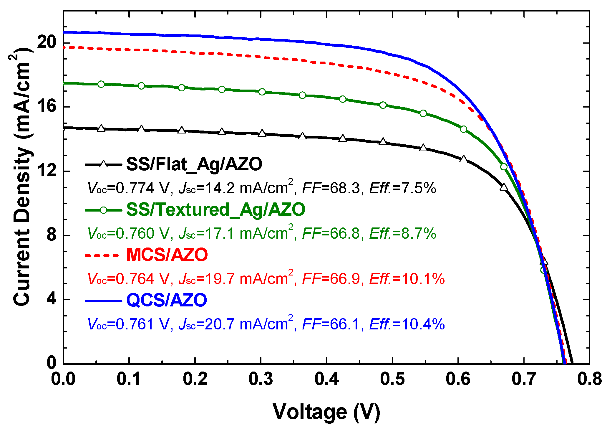
Figure 23 shows the J–V curves of a-SiGe:H solar cells with QCS/AZO, MCS/AZO, SS/flat_Ag/AZO and SS/textured_Ag/AZO BRs, respectively. The Voc and FF of the solar cell with QCS/ZnO BR are almost as high as those of solar cells with MCS/ZnO and SS/textured_Ag/AZO BRs. The Jsc are 14.2 mA/cm2 to 19.7 mA/cm2 for solar cells with MCS/ZnO and SS/flat_Ag/AZO BRs, respectively. For the solar cell with QCS/ZnO BR, the Jsc further jumps to 20.7 mA/cm2, demonstrating a relative increase of 45.8% and 21.1% with respect to the SS/flat_Ag/AZO and SS/textured_Ag/AZO BRs, respectively. For the solar cell with SS/flat_Ag/AZO BR, the conversion efficiency is 7.5%. For those solar cells with SS/textured_Ag/AZO, MCS/AZO and QCS/AZO BRs. The respective conversion efficiencies are 8.7%, 10.1% and 10.4%, corresponding to relative enhancements of 16%, 34.7% and 38.7%, respectively.
It has long been discussed which light-trapping structure, random or periodic, results in better light-trapping in solar cells, and this question remains controversial until now [56,57,58,59,60,61]. For periodic structures, large periods provide more diffraction orders than the small ones according to the grating equation, which is favorable for the resonant absorption enhancement. In addition to arousing sufficient guided mode resonances, close attention should be paid to improve the diffraction efficiency of the high order, which can lead to a highly oblique diffraction angle to remarkably elongate the optical path length. For microscale structures, it is difficult to improve the diffraction efficiency due to the large amounts of diffraction order. For nano-textured structures, only two or three diffraction peaks can be observed in the long wavelength range, which makes it easy to get high diffraction efficiency.
In this case, the diffraction efficiency of higher order can be improved via morphology control. However, if a single period is adopted, a trade-off might arise between sufficient guided mode resonances and enhanced diffraction efficiency of higher order. An alternative solution is to superimpose as many periods with different scales as possible. Another possible solution is to use a random nanotexture, as we have mentioned before that it can be decomposited into various scales of periods. If each Fourier component of the random nanotexture has the same aspect ratio with respect to the single period structure, we expect that randomly nanotextured BR could provide advantageous light-trapping performance over the periodic one with a similar lateral feature size. By combining the random nanotextures with periodic micro-textures, further absorption enhancement is expectable since richer Fourier components can be obtained with respect to the random one. In addition, it has been verified that diffracted energy can be channeled into higher diffraction orders while combining random with mesoscopic periods (periods typically 2–10 times higher than the operating wavelength, such as the MCS used here) by careful design of the modulation [62]. Therefore, besides offering the advantage of significantly improving light coupling ability, QCS also possesses a high potential of making the light-trapping effect prominent. It is noteworthy that the improved light coupling can become more effective with an outstanding light-trapping structure, since the extra light transmitted to the solar cells can be absorbed as much as possible. Briefly, the complementary of the above two effects aroused by QCS would inevitably result in a remarkable full-spectrum absorption enhancement, thus a further efficiency boost of solar cells.
4. Conclusions
After comprehensive studies of the design, simulation and fabrication of 1D-PC- and 2D-PC-based back reflectors, the following conclusions can be drawn.
A high reflectivity of 96.7% can be achieved for the 1D-PC with five periods of a 140-nm SiO2 upper layer and a 30-nm a-Si:H under layer, which is better than the DBR structure with 93.5% and a Ag film with 93.4%.
- TCPC BRs formed by combining flat 1D-PC and textured AZO can provide significant light scattering while maintaining high reflectivity. The TCPC BR-based solar cell showed an improved Jsc without deterioration of Voc and FF, resulting in much better device performance.
- RTPC BRs formed by combining textured 1D-PC and flat AZO also are excellent candidates to provide both high reflectivity and strong light scattering. An increased photocurrent density and total efficiency of a-Si:H solar cells are expectable.
- For MCPS BRs-based solar cells, absorption enhancement in the short wavelength range can contribute to the improved light coupling, while in the long wavelength range, it is realized by the co-effect of light coupling and light-trapping.
- For QCS BRs, the random nanotextures are largely flattened, while the micro-cone shapes are well preserved, resulting in a full-spectrum light coupling enhancement. Light-trapping performance is significantly improved due to the rich guided mode resonances.
Based on the above results, the next focus will be to illuminate the optimal structure design of PC-based back reflectors and to try to further improve the solar cell efficiency.
Acknowledgments
This research was supported by the National Natural Science Foundation of China (No. 61474066, 61504069, 61404074), the Natural Science Foundation of Tianjin (No. 15JCYBJC21200 and No. 14JCQNJC02100), the Programme of Introducing Talents of Discipline to Universities (B16027) and the Open Fund of the Key Laboratory of Optical Information Science & Technology (Nankai University, No. 2017KFKT015).
Conflicts of Interest
The authors declare no conflict of interest.
References
- Green, M.A. The passivated emitter and rear cell (PERC): From conception to mass production. Sol. Energy Mater. Sol. Cells 2015, 143, 190–197. [Google Scholar] [CrossRef]
- Yoshikawa, K.; Kawasaki, H.; Yoshida, W.; Irie, T.; Konishi, K.; Nakano, K.; Uto, T.; Adachi, D.; Kanematsu, M.; Uzu, H.; et al. Silicon heterojunction solar cell with interdigitated back contacts for photoconversion over 26%. Nat. Energy 2017, 2, 17032. [Google Scholar] [CrossRef]
- Schubert, M.B.; Werner, J.H. Flexible solar cells for clothing. Mater. Today 2006, 9, 42–50. [Google Scholar] [CrossRef]
- Yang, J.; Banerjee, A.; Guha, S. Amorphous silicon based photovoltaics-from earth to the “final frontier”. Sol. Energy Mater. Sol. Cells 2003, 78, 597–612. [Google Scholar] [CrossRef]
- Guha, S.; Yang, J.; Yan, B. High efficiency multi-junction thin film silicon cells incorporating nanocrystalline silicon. Sol. Energy Mater. Sol. Cells 2013, 119, 1–11. [Google Scholar] [CrossRef]
- Yoon, J.-H.; Song, J.; Lee, S.-J. Practical application of building integrated photovoltaic (BIPV) system using transparent amorphous silicon thin-film PV module. Sol. Energy 2011, 85, 723–733. [Google Scholar] [CrossRef]
- Lim, J.W.; Kim, G.; Shin, M.; Yun, S.J. Colored a-Si:H transparent solar cells employing ultrathin transparent multi-layered electrodes. Sol. Energy Mater. Sol. Cells 2017, 163, 164–169. [Google Scholar] [CrossRef]
- Kuang, P.; Eyderman, S.; Hsieh, M.L.; Post, A.; John, S.; Lin, S.Y. Achieving an accurate surface profile of a photonic crystal for near-unity solar absorption in a super thin-film architecture. ACS Nano 2016, 10, 6116–6124. [Google Scholar] [CrossRef] [PubMed]
- Sai, H.; Jia, H.; Kondo, M. Impact of front and rear texture of thin-film microcrystalline silicon solar cells on their light trapping properties. J. Appl. Phys. 2010, 108, 044505. [Google Scholar]
- Lin, Y.Y.; Xu, Z.; Yu, D.L.; Lu, L.F.; Yin, M.; Tavakoli, M.M.; Chen, X.Y.; Hao, Y.Y.; Fan, Z.Y.; Cui, Y.X.; et al. Dual-layer nanostructured flexible thin-film amorphous silicon solar cells with enhanced light harvesting and photoelectric conversion efficiency. ACS Apl. Mater. Interfaces 2016, 8, 10929–10936. [Google Scholar] [CrossRef] [PubMed]
- Sai, H.; Saito, K.; Kondo, M. Investigation of textured back reflectors with periodic honeycomb patterns in thin-film silicon solar cells for improved photovoltaic performance. IEEE J. Photovolt. 2013, 3, 5–10. [Google Scholar] [CrossRef]
- Paetzold, U.W.; Lehnen, S.; Bittkau, K.; Rau, U.; Carius, R. Nanoscale observation of waveguide modes enhancing the efficiency of solar cells. Nano Lett. 2014, 14, 6599–6605. [Google Scholar] [CrossRef] [PubMed]
- Tan, H.; Moulin, E.; Si, F.T.; Schuttauf, J.W.; Stuckelberger, M.; Isabella, O.; Haug, F.J.; Ballif, C.; Zeman, M.; Smets, A.H.M. Highly transparent modulated surface textured front electrodes for high-efficiency multijunction thin-film silicon solar cells. Prog. Photovolt. 2015, 23, 949–963. [Google Scholar] [CrossRef]
- Soderstrom, T.; Haug, F.J.; Niquille, X.; Ballif, C. TCOs for nip thin film silicon solar cells. Prog. Photovolt. 2009, 17, 165–176. [Google Scholar] [CrossRef]
- Yan, B.; Yue, G.; Sivec, L.; Owens-Mawson, J.; Yang, J.; Guha, S. Correlation of texture of Ag/ZnO back reflector and photocurrent in hydrogenated nanocrystalline silicon solar cells. Sol. Energ. Mat. Sol. Cells 2012, 104, 13–17. [Google Scholar] [CrossRef]
- Isabella, O.; Krc, J.; Zeman, M. Modulated surface textures for enhanced lighttrapping in thin-film silicon solar cells. Appl. Phys. Lett. 2010, 97, 101106. [Google Scholar] [CrossRef]
- Tan, H.; Santbergen, R.; Smets, H.M.; Zeman, M. Plasmonic light trapping in thin-film silicon solar cells with improved self-assembled silver nanoparticles. Nano Lett. 2012, 12, 4070–4076. [Google Scholar] [CrossRef] [PubMed]
- Van Dijk, L.; van de Groep, J.; Veldhuizen, L.W.; di Vece, M.; Polman, A.; Schropp, R.E.I. Plasmonic scattering back reflector for light trapping in flat nano-crystalline silicon solar cells. ACS Photonics 2016, 3, 685–691. [Google Scholar] [CrossRef]
- Sai, H.; Matsui, T.; Koida, T.; Matsubara, K.; Kondo, M.; Sugiyama, S.; Katayama, H.; Takeuchi, Y.; Yoshida, I. Triple-junction thin-film silicon solar cell fabricated on periodically textured substrate with a stabilized efficiency of 13.6%. Appl. Phys. Lett. 2015, 106, 213902. [Google Scholar]
- Polman, A.; Atwater, H.A. Photonic design principles for ultrahigh-efficiency photovoltaics. Nat. Mater. 2012, 11, 174–177. [Google Scholar] [CrossRef] [PubMed]
- Bermel, P.; Luo, C.; Zeng, L.; Kimerling, L.C.; Joannopoulos, J.D. Improving thin-film crystalline silicon solar cell efficiencies with photonic crystals. Opt. Express 2007, 15, 16986–17000. [Google Scholar] [CrossRef] [PubMed]
- Zeng, L.; Bermel, P.; Yi, Y.; Alamariu, B.A.; Broderick, K.A.; Liu, J.; Hong, C.; Duan, X.; Joannopoulos, J.; Kimerling, L.C. Demonstration of enhanced absorption in thin film Si solar cells with textured photonic crystal back reflector. Appl. Phys. Lett. 2008, 93, 221105. [Google Scholar] [CrossRef]
- Zeng, L.; Yi, Y.; Hong, C.; Liu, J.; Feng, N.; Duan, X.; Kimerling, L.C.; Alamariu, B.A. Efficiency enhancement in Si solar cells by textured photonic crystal back reflector. Appl. Phys. Lett. 2006, 89, 111111. [Google Scholar] [CrossRef]
- O’Brien, P.G.; Kherani, N.P.; Chutinan, A.; Ozin, G.A.; John, S.; Zukotynski, S. Silicon photovoltaics using conducting photonic crystal back-reflectors. Adv. Mater. 2008, 20, 1577–1582. [Google Scholar] [CrossRef]
- Krc, J.; Zeman, M.; Luxembourg, S.L.; Topic, M. Modulated photonic-crystal structures as broadband back reflectors in thin film solar cells. Appl. Phys. Lett. 2009, 94, 153501. [Google Scholar] [CrossRef]
- Isebella, O.; Dobrovolskiy, S.; Kroon, G.; Zeman, M. Design and application of dielectric distributed Bragg back reflector in thin-film silicon solar cells. J. Non-Cryst. Solids 2012, 358, 2295–2298. [Google Scholar] [CrossRef]
- Chen, P.Z.; Hou, G.F.; Zhang, J.J.; Zhang, X.D.; Zhao, Y. Optimal design of one-dimensional photonic crystal back reflectors for thin-film silicon solar cells. J. Appl. Phys. 2014, 116, 064508. [Google Scholar] [CrossRef]
- Hoffmann, A.; Paetzold, U.W.; Zhang, C.; Merdzhanova, T.; Lambertz, A.; Ulbrich, C.; Bittkau, K.; Rau, U. Advancing tandem solar cells by spectrally selective multilayer intermediate reflectors. Opt. Express 2014, 22, A1270–A1277. [Google Scholar] [CrossRef] [PubMed]
- Chen, Z.P.; Hou, G.F.; Fan, Q.H.; Huang, Q.; Zhao, J.; Zhang, J.J.; Ni, J.; Zhang, X.D.; Zhao, Y. An efficient light trapping scheme based on textured conductive photonic crystal back reflector for performance improvement of amorphous silicon solar cells. Appl. Phys. Lett. 2014, 105, 073506. [Google Scholar] [CrossRef]
- Zhou, D.Y.; Biswas, R. Photonic crystal enhanced light trapping in thin film solar cells. J. Appl. Phys. 2008, 103, 093102. [Google Scholar] [CrossRef]
- Mutitu, J.G.; Shi, S.Y.; Chen, C.H.; Creazzo, T.; Barnett, A.; Honsberg, C.; Prather, D.W. Thin film silicon solar cell design based on photonic crystal and diffractive grating structures. Opt. Express 2008, 16, 15238–15248. [Google Scholar] [CrossRef] [PubMed]
- Sai, H.; Kanamori, Y.; Kondo, M. Flattened light-scattering substrate in thin film silicon solar cells for improved infrared response. Appl. Phys. Lett. 2011, 98, 113502. [Google Scholar] [CrossRef]
- Vetterl, O.; Finger, F.; Carius, R.; Hapke, P.; Houben, L.; Kluth, O.; Lambertz, A.; Muck, A.; Rech, B.; Wagner, H. Intrinsic microcrystalline silicon: A new material for photovoltaics. Sol. Energy Mater. Sol. Cells 2000, 62, 97–108. [Google Scholar] [CrossRef]
- Shah, A.V.; Schade, H.; Vanecek, M.; Meier, J.; Vallat-Sauvain, E.; Wyrsch, N.; Kroll, U.; Droz, C.; Bailat, J. Thin-film silicon solar cell technology. Prog. Photovolt. 2004, 12, 113–142. [Google Scholar] [CrossRef]
- Muller, J.; Rech, B.; Springer, J.; Vanecek, M. TCO and light trapping in silicon thin film solar cells. Sol. Energy 2004, 77, 917–930. [Google Scholar] [CrossRef]
- Agashe, C.; Kluth, O.; Hupkes, J.; Zastrow, U.; Rech, B.; Wuttig, M. Efforts to improve carrier mobility in radio frequency sputtered aluminum doped zinc oxide films. J. Appl. Phys. 2004, 95, 1911–1917. [Google Scholar] [CrossRef] [Green Version]
- Haug, F.J.; Soederstroem, T.; Cubero, O.; Terrazzoni-Daudrix, V.; Ballif, C. Plasmonic absorption in textured silver back reflectors of thin film solar cells. J. Appl. Phys. 2008, 104, 064509. [Google Scholar] [CrossRef]
- Curtin, B.; Biswas, R.; Dalal, V. Photonic crystal based back reflectors for light management and enhanced absorption in amorphous silicon solar cells. Appl. Phys. Lett. 2009, 95, 231102. [Google Scholar] [CrossRef]
- Zhao, Y.; Miyajima, S.; Ide, Y.; Yamada, A.; Konagai, M. Microcrystalline silicon films and solar cells prepared by photochemical vapor deposition on textured SnO2 with high haze factors. Jpn. J. Appl. Phys. 2002, 41, 6417. [Google Scholar] [CrossRef]
- Yue, G.; Sivec, L.; Owens, J.M.; Yan, B.; Yang, J.; Guha, S. Optimization of back reflector for high efficiency hydrogenated nanocrystalline silicon solar cells. Appl. Phys. Lett. 2009, 95, 263501. [Google Scholar] [CrossRef]
- Sai, H.; Saito, K.; Hozuki, N.; Kondo, M. Relationship between the cell thickness and the optimum period of textured back reflectors in thin-film microcrystalline silicon solar cells. Appl. Phys. Lett. 2013, 102, 053509. [Google Scholar]
- Yin, J.; Zhu, H.; Wang, Y.; Wang, Z.; Gao, J.; Mai, Y.; Ma, Y.; Wan, M.; Huang, Y. A study of ZnO:B films for thin film silicon solar cells. Appl. Surf. Sci. 2012, 259, 758–763. [Google Scholar] [CrossRef]
- Chen, P.; Hou, G.; Fan, Q.; Ni, J.; Zhang, J.; Huang, Q.; Zhang, X.; Zhao, Y. Combining randomly textured surfaces and one-dimensional photonic crystals as efficient light-trapping structures in hydrogenated amorphous silicon solar cells. Sol. Energy Mater. Sol. Cells 2015, 143, 435–441. [Google Scholar] [CrossRef]
- Yan, B.; Yue, G.; Sivec, L.; Yang, J.; Guha, S.; Jiang, C.-S. Innovative dual function nc-SiOx:H layer leading to a 16% efficient multi-junction thin-film silicon solar cell. Appl. Phys. Lett. 2011, 99, 113512. [Google Scholar] [CrossRef]
- Hsu, Y.T.; Yu, C.C.; Huang, K.F.; Lan, W.H.; Huang, J.E.; Lin, J.C.; Lin, W.J. Improved output power of nitride-based light-emitting diodes with convex-patterned sapphire substrates. IEEE Photonic. Tech. Lett. 2012, 24, 1686–1688. [Google Scholar] [CrossRef]
- Zhou, S.J.; Cao, B.; Liu, S.; Ding, H. Improved light extraction efficiency of gan-based leds with patterned sapphire substrate and patterned ITO. Opt. Laser Technol. 2012, 44, 2302–2305. [Google Scholar] [CrossRef]
- Chen, P.; Niu, P.; Yu, L.; Zhang, J.; Fan, Q.H.; Yang, G.; Ning, P.; Hou, G. Periodically patterned micro-cone textures as high-efficiency light harvesting structure for broadband absorption enhancement in thin film silicon solar cells. Sol. Energy 2018, 159. [Google Scholar]
- Tan, H.; Sivec, L.; Yan, B.; Santbergen, R.; Zeman, M.; Smets, A.H.M. Improved light trapping in microcrystalline silicon solar cells by plasmonic back reflector with broad angular scattering and low parasitic absorption. Appl. Phys. Lett. 2013, 102, 153902. [Google Scholar] [CrossRef]
- Yang, X. Study of Transparent Conducting Oxides and Back Reflectors for Amorphous and Nanocrystalline Silicon Based Thin Film Solar Cells. Ph.D. Thesis, The university of Toledo, Toledo, OH, USA, December 2007. [Google Scholar]
- Sai, H.; Matsui, T.; Saito, K.; Kondo, M.; Yoshida, I. Photocurrent enhancement in thin-film silicon solar cells by combination of anti-reflective sub-wavelength structures and light-trapping textures. Prog. Photovolt. 2015, 23, 1572–1580. [Google Scholar] [CrossRef]
- Chang, C.H.; Dominguez-Gaballero, J.A.; Choi, H.J.; Barbastathis, G. Nanostructured gradient-index antireflection diffractive optics. Opt. Lett. 2011, 36, 2354–2356. [Google Scholar] [CrossRef] [PubMed]
- Rowlands, S.F.; Livingstone, J.; Lund, C.P. Optical modelling of thin film solar cells with textured interfaces using the effective medium approximation. Sol. Energy 2004, 76, 301–307. [Google Scholar] [CrossRef]
- Dewan, R.; Shrestha, S.; Jovanov, V.; Hupkes, J.; Bittkau, K.; Knipp, D. Random versus periodic: Determining light trapping of randomly textured thin film solar cells by the superposition of periodic surface textures. Sol. Energ. Mat. Sol. Cells 2015, 143, 183–189. [Google Scholar] [CrossRef]
- Sun, Y.Q.; Wu, Z.H.; Yin, J.; Fang, Y.Y.; Wang, H.; Yu, C.H.; Hui, X.O.; Chen, C.Q.; Wei, Q.Y.; Li, T.; et al. High quality a-plane GaN films grown on cone-shaped patterned r-plane sapphire substrates. Thin Solid Films 2011, 519, 2508–2512. [Google Scholar] [CrossRef]
- Chen, P.; Niu, P.; Yu, L.; Zhang, J.; Fan, Q.H.; Yang, G.; Fu, X.; Hou, G. Quasi-crystal photonic structures for fullband absorption enhancement in thin film silicon solar cells. Sol. Energy Mater. Sol. Cells 2018, 175. [Google Scholar]
- Sheng, P.; Bloch, A.N.; Stepleman, R.S. Wavelength selective absorption enhancement in thin-film solar cells. Appl. Phys. Lett. 1983, 43, 579–581. [Google Scholar] [CrossRef]
- Eisele, C.; Nebel, C.E.; Stutzmann, M. Periodic light coupler gratings in amorphous thin film solar cells. J. Appl. Phys. 2001, 89, 7722–7726. [Google Scholar] [CrossRef]
- Stiebig, H.; Senoussaoui, N.; Zahren, C.; Haase, C.; Müller, J. Silicon thin-film solar cells with rectangular-shaped grating coupler. Prog. Photovolt. 2006, 14, 13–24. [Google Scholar] [CrossRef]
- Ferry, V.E.; Verschuuren, M.A.; van Lare, M.C.; Schropp, R.E.I.; Atwater, H.A.; Polman, A. Optimized spatial correlations for broadband light trapping nanopatterns in high efficiency ultrathin film a-Si:H solar cells. Nano Lett. 2011, 11, 4239–4245. [Google Scholar] [CrossRef] [PubMed]
- Battaglia, C.; Hsu, C.; Soderstrom, K.; Escarre, J.; Haug, F.; Charriere, M.; Boccard, M.; Despeisse, M.; Alexander, D.T.L.; Cantoni, M.; Cui, Y.; Ballif, C. Light trapping in solar cells: Can periodic beat random? ACS Nano 2012, 6, 2790–2797. [Google Scholar] [CrossRef] [PubMed]
- Dewan, R.; Jovanov, V.; Hamraz, S.; Knipp, D. Analyzing periodic and random textured silicon thin film solar cells by rigorous coupled wave analysis. Sci. Rep. 2014, 4, 6029. [Google Scholar] [CrossRef] [PubMed]
- Martins, E.R.; Li, J.; Liu, Y.; Depauw, V.; Chen, Z.; Zhou, J.; Krauss, T.F. Deterministic quasi-random nanostructures for photon control. Nat. Commun. 2013, 4, 2665. [Google Scholar] [CrossRef] [PubMed]
Figure 1.
Schematic of a 1D photonic crystal (PC) formed by periodically stacking of a-Si:H high-n layers and SiO2 low-n layers.
Figure 1.
Schematic of a 1D photonic crystal (PC) formed by periodically stacking of a-Si:H high-n layers and SiO2 low-n layers.

Figure 2.
Average reflectivity in the wavelength range of 520–800 nm and the periodic thickness as a function of the Bragg wavelength. The distributed Bragg reflector (DBR) structure consists of five periods of a high-n a-Si:H layer and a low-n SiO2 layer. (Reproduced from [27], with the permission of AIP Publishing.)
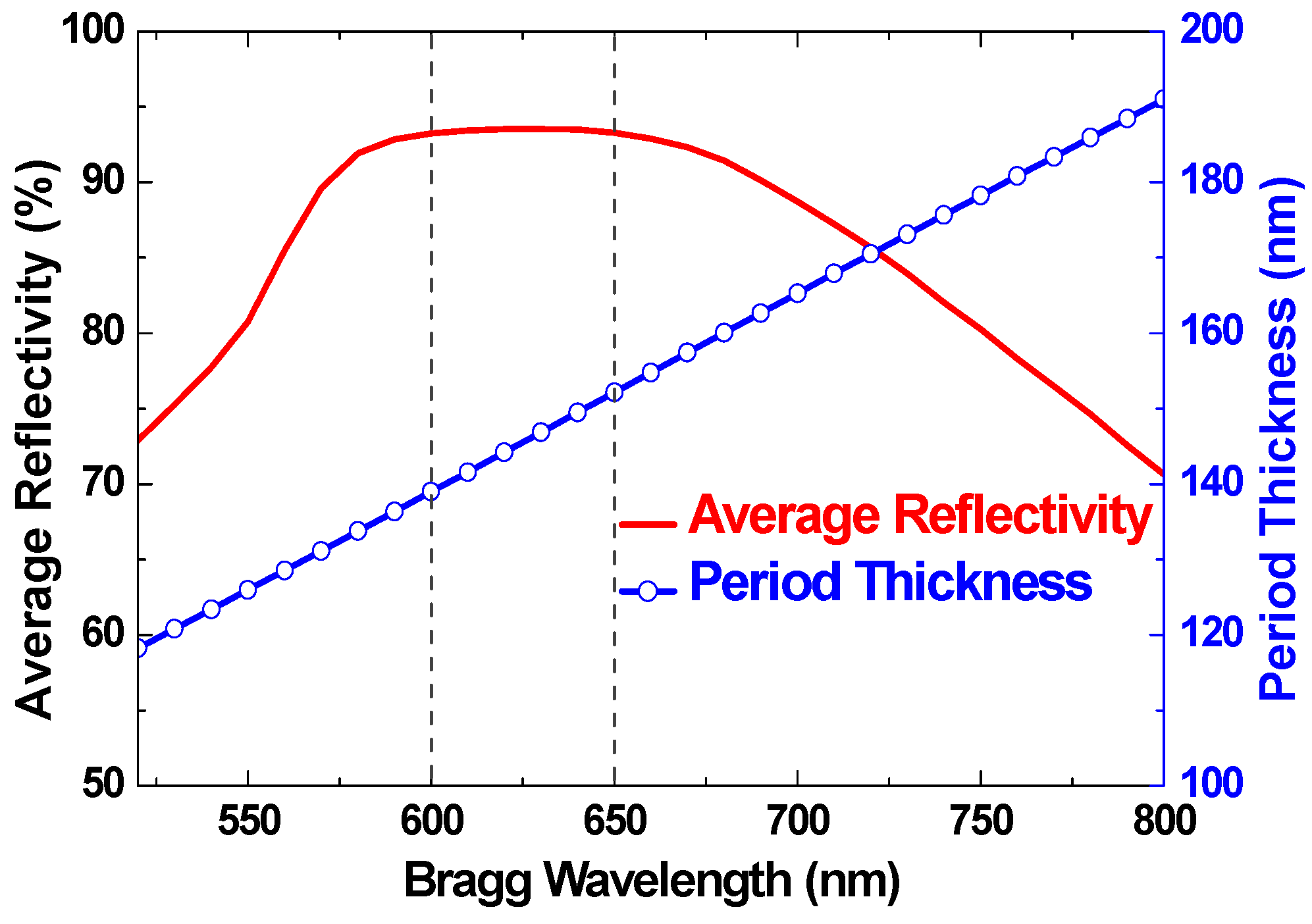
Figure 3.
The photonic bandgap (PBG) as a function of thickness-contrast with three different refractive index contrasts (3/1.5, 4/1.5 and 5/1.5). The data of the horizontal axis are the thicknesses of the high-n and low-n layers, while the periodic thickness is 150 nm. (Reproduced from [27], with the permission of AIP Publishing.)

Figure 4.
Simulated reflection curves of 1D-PC with thickness-contrasts (high-n/low-n layer) of 30 nm/120 nm, optimal DBR with thickness-contrasts of 40 nm/110 nm, 1D-PC with thickness-contrasts of 30 nm/140 nm and the Ag film. T_30 nm/140 nm is the transmission curve for 30 nm/140 nm. (Reproduced from [27], with the permission of AIP Publishing.)

Figure 5.
Schematic diagram of an n-i-p a-Si:H solar cell with the texture conductive photonic crystal (TCPC) BR. (Reproduced from [29], with the permission of AIP Publishing.)
Figure 5.
Schematic diagram of an n-i-p a-Si:H solar cell with the texture conductive photonic crystal (TCPC) BR. (Reproduced from [29], with the permission of AIP Publishing.)
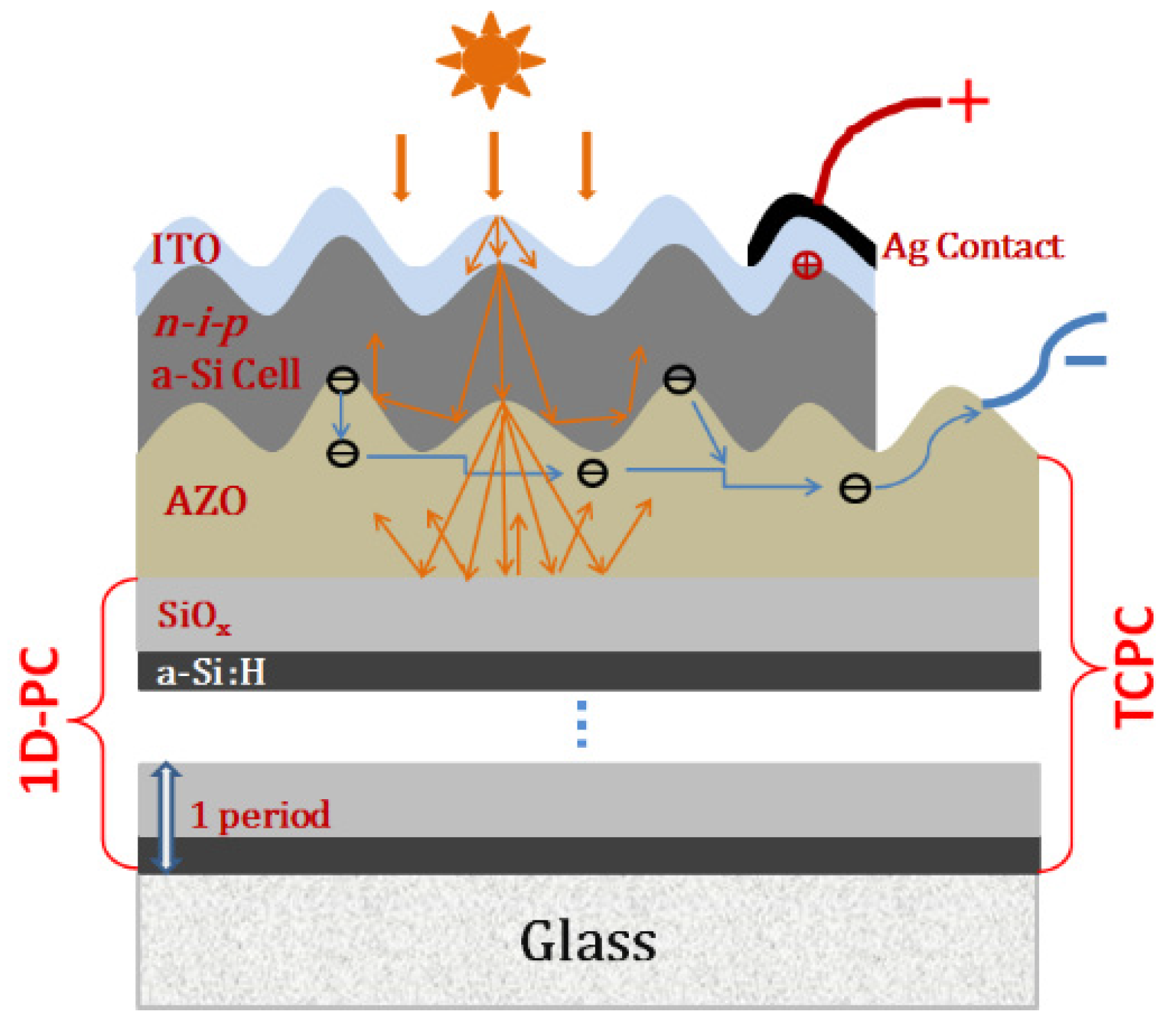
Figure 6.
Cross-sectional SEM images of (a) CPC and (b) TCPC. (Reproduced from [29], with the permission of AIP Publishing.)
Figure 6.
Cross-sectional SEM images of (a) CPC and (b) TCPC. (Reproduced from [29], with the permission of AIP Publishing.)

Figure 7.
AFM images of (a) TCPC and (b) textured AZO/Ag. (Reproduced from [29], with the permission of AIP Publishing.)
Figure 7.
AFM images of (a) TCPC and (b) textured AZO/Ag. (Reproduced from [29], with the permission of AIP Publishing.)
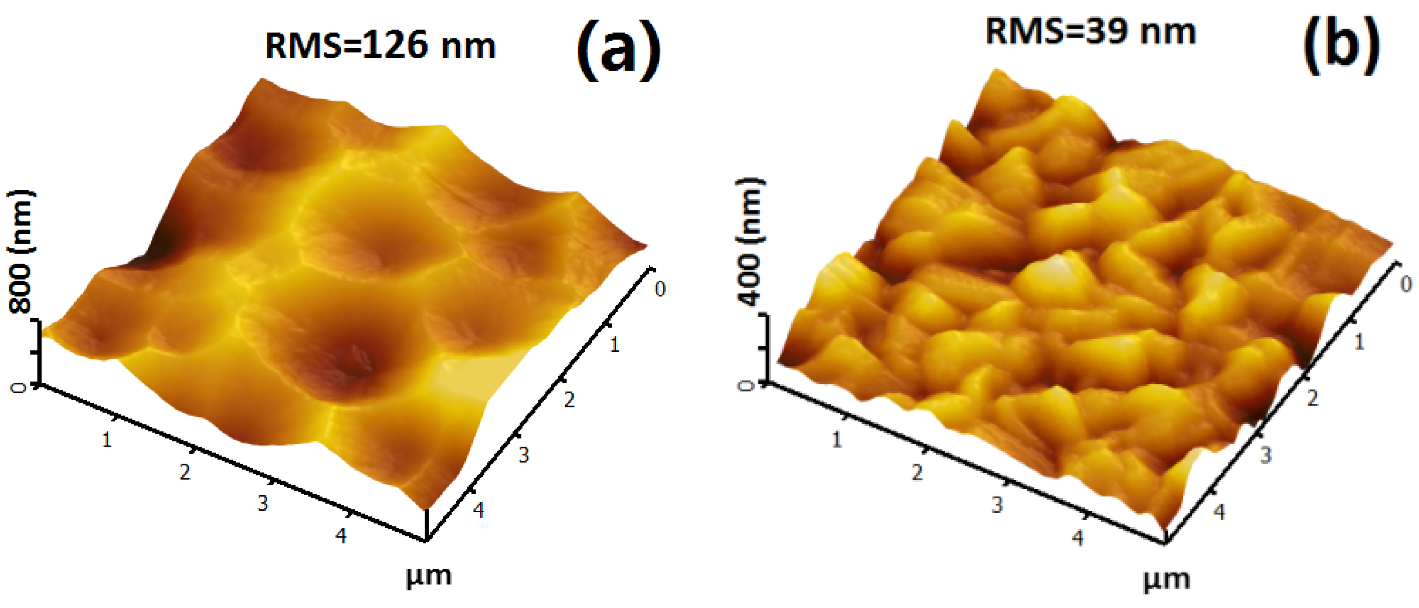
Figure 8.
(a) Total reflectance (TR) and transmittance (TT) curves; (b) haze factor of TCPC, 1D-PC, CPC and textured AZO/Ag. (Reproduced from [29], with the permission of AIP Publishing.)
Figure 8.
(a) Total reflectance (TR) and transmittance (TT) curves; (b) haze factor of TCPC, 1D-PC, CPC and textured AZO/Ag. (Reproduced from [29], with the permission of AIP Publishing.)

Figure 9.
(a) J–V curves, and (b) EQE curves of a-Si:H solar cells with different BRs (CPC, TCPC, textured AZO/Ag). (Reproduced from [29], with the permission of AIP Publishing.)
Figure 9.
(a) J–V curves, and (b) EQE curves of a-Si:H solar cells with different BRs (CPC, TCPC, textured AZO/Ag). (Reproduced from [29], with the permission of AIP Publishing.)

Figure 10.
Schematic diagram of an n-i-p a-Si:H solar cell with a novel RTPC BR. RTPC, randomly-textured photonic crystal [43]. (Reproduced from [43] with permission; Copyright 2015 Elsevier).

Figure 11.
AFM images of (a) AZO1, (b) RTPC1 on AZO1, (c) AZO2, (d) RTPC2 on AZO2 and (e) randomly textured AZO/Ag. (Reproduced from [43] with permission; Copyright 2015 Elsevier).
Figure 11.
AFM images of (a) AZO1, (b) RTPC1 on AZO1, (c) AZO2, (d) RTPC2 on AZO2 and (e) randomly textured AZO/Ag. (Reproduced from [43] with permission; Copyright 2015 Elsevier).

Figure 12.
(a) Total reflectance (TR) and transmittance (TT), and (b) haze factor of the flat 1D-PC, RTPC1 and RTPC2. (Reproduced from [43] with permission; Copyright 2015 Elsevier).
Figure 12.
(a) Total reflectance (TR) and transmittance (TT), and (b) haze factor of the flat 1D-PC, RTPC1 and RTPC2. (Reproduced from [43] with permission; Copyright 2015 Elsevier).
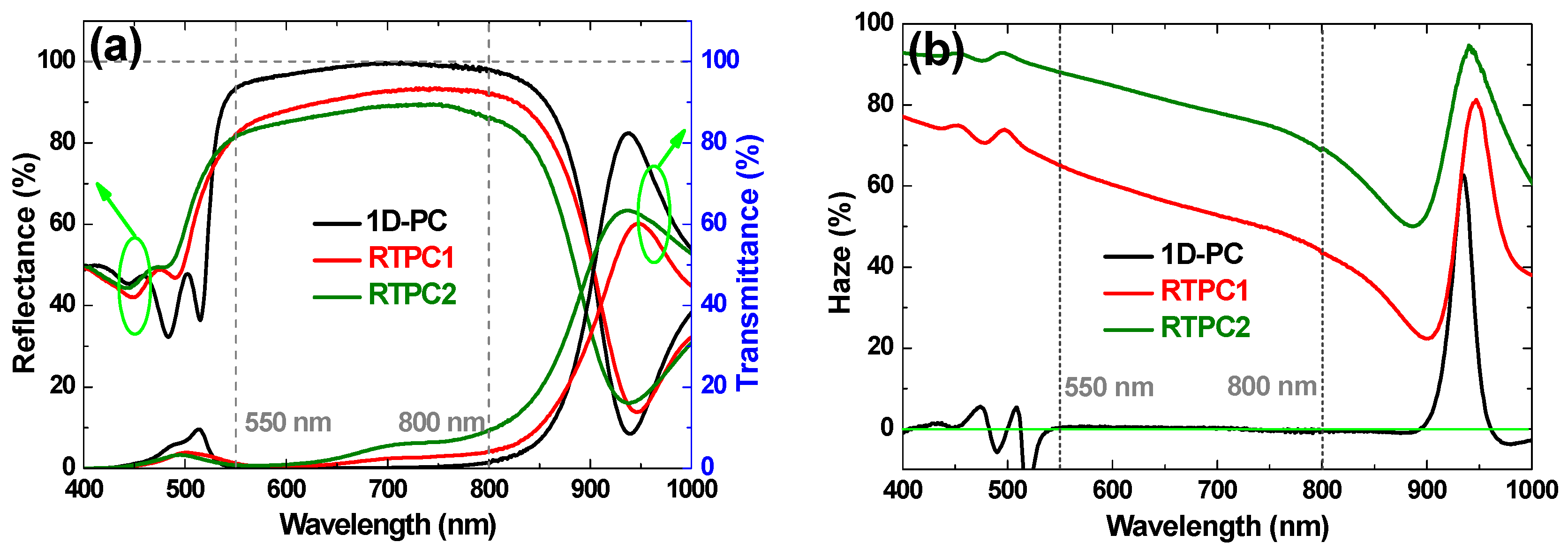
Figure 13.
(a) Total reflectance (TR) and transmittance (TT) curves; (b) haze factor of AZO/1D-PC, AZO/RTPC1, AZO/RTPC2 and randomly-textured AZO/Ag. (Reproduced from [43] with permission; Copyright 2015 Elsevier).
Figure 13.
(a) Total reflectance (TR) and transmittance (TT) curves; (b) haze factor of AZO/1D-PC, AZO/RTPC1, AZO/RTPC2 and randomly-textured AZO/Ag. (Reproduced from [43] with permission; Copyright 2015 Elsevier).

Figure 14.
(a) J–V curves, and (b) EQE curves for a-Si:H solar cells with different BRs (AZO/1D-PC, AZO/RTPC1, AZO/RTPC2 and randomly-textured AZO/Ag). (Reproduced from [43] with permission; Copyright 2015 Elsevier).
Figure 14.
(a) J–V curves, and (b) EQE curves for a-Si:H solar cells with different BRs (AZO/1D-PC, AZO/RTPC1, AZO/RTPC2 and randomly-textured AZO/Ag). (Reproduced from [43] with permission; Copyright 2015 Elsevier).

Figure 15.
(a) SEM image of a micro-cone patterned substrate (MCPS) with a uniform micro-cone pattern; (b) schematic structure of the micro-cone pattern; (c–e) cross-sectional SEM images of MCPSs with different H/P. (Reproduced from [47] with permission; Copyright 2018 Elsevier.)
Figure 15.
(a) SEM image of a micro-cone patterned substrate (MCPS) with a uniform micro-cone pattern; (b) schematic structure of the micro-cone pattern; (c–e) cross-sectional SEM images of MCPSs with different H/P. (Reproduced from [47] with permission; Copyright 2018 Elsevier.)
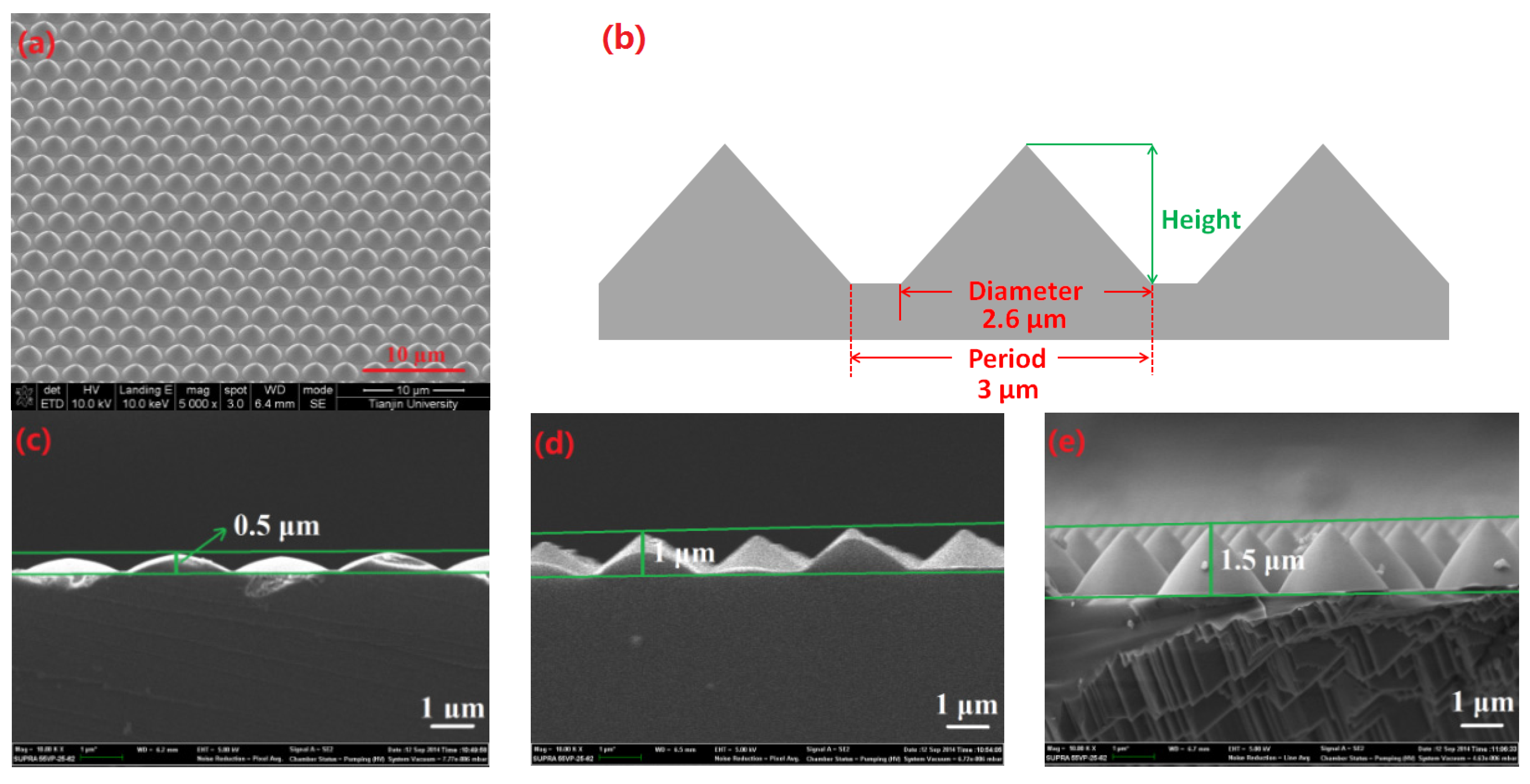
Figure 16.
SEM images of MCPS (P3H0.5, P3H1.0, P3H1.5), MCPS coated with Ag/AZO and corresponding solar cells. (Reproduced from [47] with permission; Copyright 2018 Elsevier.)
Figure 16.
SEM images of MCPS (P3H0.5, P3H1.0, P3H1.5), MCPS coated with Ag/AZO and corresponding solar cells. (Reproduced from [47] with permission; Copyright 2018 Elsevier.)
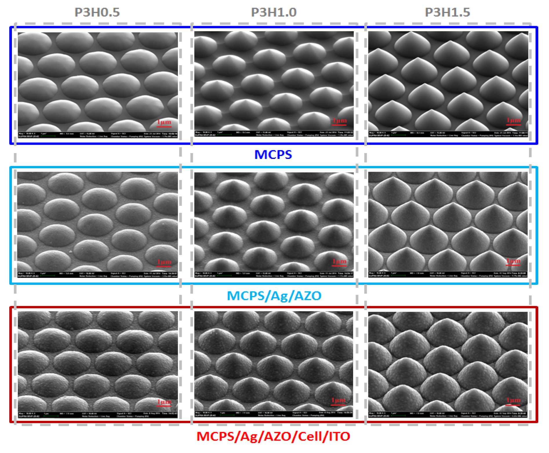
Figure 17.
(a) Total reflectance, and (b) haze factor of P3H0.5/Ag/AZO, P3H1.0/Ag/AZO, P3H1.5/Ag/AZO, SS/flat_Ag/AZO and SS/textured_Ag/AZO BRs. (Reproduced from [47] with permission; Copyright 2018 Elsevier.)
Figure 17.
(a) Total reflectance, and (b) haze factor of P3H0.5/Ag/AZO, P3H1.0/Ag/AZO, P3H1.5/Ag/AZO, SS/flat_Ag/AZO and SS/textured_Ag/AZO BRs. (Reproduced from [47] with permission; Copyright 2018 Elsevier.)

Figure 18.
(a) Total absorptance (1 − R), and (b) EQE of a-SiGe:H solar cells with P3H0.5/Ag/AZO, P3H1.0/Ag/AZO, P3H1.5/Ag/AZO, SS/flat_Ag/AZO and SS/textured_Ag/AZO BRs. (Reproduced from [47] with permission; Copyright 2018 Elsevier.)
Figure 18.
(a) Total absorptance (1 − R), and (b) EQE of a-SiGe:H solar cells with P3H0.5/Ag/AZO, P3H1.0/Ag/AZO, P3H1.5/Ag/AZO, SS/flat_Ag/AZO and SS/textured_Ag/AZO BRs. (Reproduced from [47] with permission; Copyright 2018 Elsevier.)

Figure 19.
J–V curves of a-SiGe:H solar cells withP3H0.5/Ag/AZO, P3H1.0/Ag/AZO, P3H1.5/Ag/AZO, SS/flat_Ag/AZO and SS/textured_Ag/AZO BRs. (Reproduced from [47] with permission; Copyright 2018 Elsevier.)
Figure 19.
J–V curves of a-SiGe:H solar cells withP3H0.5/Ag/AZO, P3H1.0/Ag/AZO, P3H1.5/Ag/AZO, SS/flat_Ag/AZO and SS/textured_Ag/AZO BRs. (Reproduced from [47] with permission; Copyright 2018 Elsevier.)

Figure 20.
SEM images of micro-cone structure (MCS), quasi-crystal structure (QCS), MCS-based and QCS-based a-SiGe:H solar cells. (Reproduced from [55] with permission; Copyright 2018 Elsevier.)
Figure 20.
SEM images of micro-cone structure (MCS), quasi-crystal structure (QCS), MCS-based and QCS-based a-SiGe:H solar cells. (Reproduced from [55] with permission; Copyright 2018 Elsevier.)
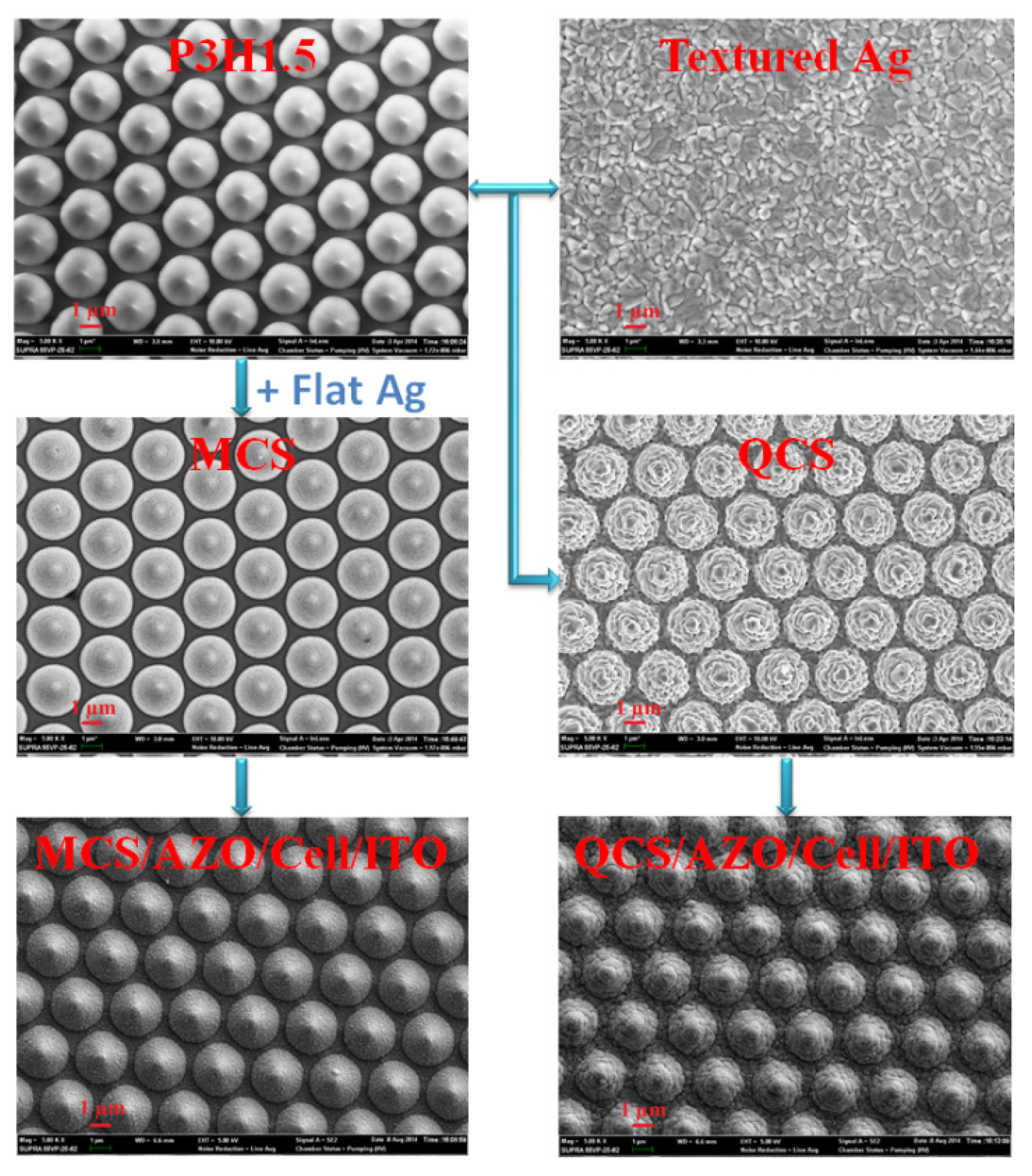
Figure 21.
(a) Total reflectance, and (b) haze factor of SS/Flat_Ag/AZO, SS/textured_Ag/AZO, MCS/AZO, QCS/AZO BRs. (Reproduced from [55] with permission; Copyright 2018 Elsevier.)
Figure 21.
(a) Total reflectance, and (b) haze factor of SS/Flat_Ag/AZO, SS/textured_Ag/AZO, MCS/AZO, QCS/AZO BRs. (Reproduced from [55] with permission; Copyright 2018 Elsevier.)

Figure 22.
(a) Total absorptance (1 − R) curves, and (b) EQE curves of a-SiGe:H solar cells with different BRs (SS/Flat_Ag/AZO, SS/textured_Ag/AZO, MCS/AZO, QCS/AZO). (Reproduced from [55] with permission; Copyright 2018 Elsevier.)
Figure 22.
(a) Total absorptance (1 − R) curves, and (b) EQE curves of a-SiGe:H solar cells with different BRs (SS/Flat_Ag/AZO, SS/textured_Ag/AZO, MCS/AZO, QCS/AZO). (Reproduced from [55] with permission; Copyright 2018 Elsevier.)
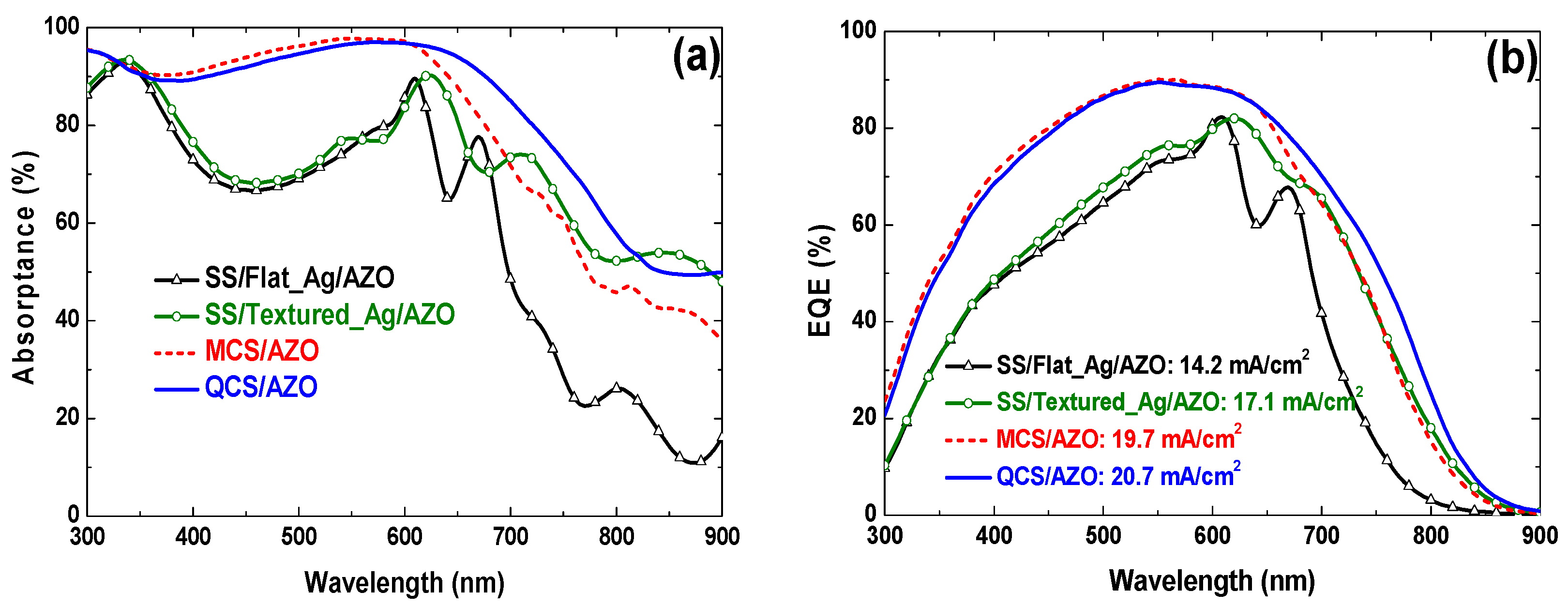
Figure 23.
J–V curves of a-SiGe:H solar cells with SS/Flat_Ag/AZO, SS/textured_Ag/AZO, MCS/AZO, QCS/AZO BRs. (Reproduced from [55] with permission; Copyright 2018 Elsevier.)
Figure 23.
J–V curves of a-SiGe:H solar cells with SS/Flat_Ag/AZO, SS/textured_Ag/AZO, MCS/AZO, QCS/AZO BRs. (Reproduced from [55] with permission; Copyright 2018 Elsevier.)
© 2017 by the authors. Licensee MDPI, Basel, Switzerland. This article is an open access article distributed under the terms and conditions of the Creative Commons Attribution (CC BY) license (http://creativecommons.org/licenses/by/4.0/).
Share and Cite
MDPI and ACS Style
Ding, Y.; Chen, P.; Fan, Q.H.; Hou, G. Photonic Structures for Light Trapping in Thin Film Silicon Solar Cells: Design and Experiment. Coatings 2017, 7, 236. https://doi.org/10.3390/coatings7120236
AMA Style
Ding Y, Chen P, Fan QH, Hou G. Photonic Structures for Light Trapping in Thin Film Silicon Solar Cells: Design and Experiment. Coatings. 2017; 7(12):236. https://doi.org/10.3390/coatings7120236
Chicago/Turabian StyleDing, Yi, Peizhuan Chen, Qi Hua Fan, and Guofu Hou. 2017. "Photonic Structures for Light Trapping in Thin Film Silicon Solar Cells: Design and Experiment" Coatings 7, no. 12: 236. https://doi.org/10.3390/coatings7120236
Note that from the first issue of 2016, this journal uses article numbers instead of page numbers. See further details here.