Article

Silicides and Nitrides Formation in Ti Films Coated on Si and Exposed to (Ar-N2-H2) Expanding Plasma

1
Faculté des Sciences et Techniques, Université de Limoges, CNRS, ENSCI, SPCTS, UMR7315, CEC, 12 rue Atlantis, F-87068 Limoges, France
2
Institut Jean Lamour, CNRS, Université de Lorraine, UMR7198, Parc de Saurupt F-54011 Nancy, France
3
Faculté des Sciences et Techniques, Université de Limoges, CNRS, XLIM, UMR6172, 123 av. A. Thomas, F-87060 Limoges, France
*
Author to whom correspondence should be addressed.
Coatings 2017, 7(2), 23; https://doi.org/10.3390/coatings7020023
Submission received: 20 September 2016 / Revised: 20 January 2017 / Accepted: 4 February 2017 / Published: 8 February 2017

Abstract

:
The physical properties including the mechanical, optical and electrical properties of Ti nitrides and silicides are very attractive for many applications such as protective coatings, barriers of diffusion, interconnects and so on. The simultaneous formation of nitrides and silicides in Ti films improves their electrical properties. Ti films coated on Si wafers are heated at various temperatures and processed in expanding microwave (Ar-N2-H2) plasma for various treatment durations. The Ti-Si interface is the centre of Si diffusion into the Ti lattice and the formation of various Ti silicides, while the Ti surface is the centre of N diffusion into the Ti film and the formation of Ti nitrides. The growth of silicides and nitrides gives rise to two competing processes which are thermodynamically and kinetically controlled. The effect of thickness on the kinetics of the formation of silicides is identified. The metastable C49TiSi2 phase is the main precursor of the stable C54TiSi2 phase, which crystallizes at about 600 °C, while TiN crystallizes at about 800 °C.

1. Introduction

The very attractive physical and chemical properties of titanium nitrides (TiN) make them very efficient for a great number of applications [1,2,3,4,5,6,7,8,9,10,11]. TiN exhibits a high melting point of 3220 K greater than those of ceramic materials such as Al2O3 or Si3N4. Owing to their extreme hardness, high thermodynamic stability, low friction constant, high wear and corrosion resistance, they are used as protective coatings in many industries. Their beautiful golden colours find applications in decorative coatings. Their optical properties make them very interesting for applications in solar cells, antireflective coatings, optical filters and plasmonics. Because of the plasmonic response of TiN, they are promising to replace nanoparticles of noble metals which show low melting points and high conduction electron losses [2]. TiN films are also good diffusion barriers for metal interconnects. Moreover, owing to their very low resistivity of 30 μΩ·cm, TiN films can replace silicon as gate electrodes in metal oxide semiconductor (MOS) devices as well as upper electrodes in Schottky diodes [1].
The equilibrium phases diagram of Ti-N [12] shows the Ti2N and TiN phases beside the solid solution of nitrogen in titanium αTi and βTi, depending on temperature. The Ti2N phase crystallizes either in the tetragonal structure or in the base-centred tetragonal structure with a small range of composition of about 33.3 at.% and 37.5 at.% of nitrogen, respectively. The TiNx phase has a NaCl-type crystal structure with a wide range of composition from x = 0.6 to 1.2 [13].
In the same way, transition metal silicides find applications as contacts and interconnects in MOS silicon integrated circuits for reducing the resistance of polysilicon gates and source/drain diffusion regions, because of their high temperature stability, low resistivity, chemical compatibility, electromigration resistance, and low barrier height [9,14].
Owing to the formation of several different compounds during thermal annealing of Ti films coated on Si substrates, Ti-Si interaction is very complex. The metastable C49TiSi2 phase of base-centred orthorhombic structure crystallizes at temperatures of 450–600 °C whereas the thermodynamically stable C54TiSi2 phase of face-centred orthorhombic structure is formed at temperatures greater than 650 °C [15]. Other Ti-Si phases have been detected during thermal annealing, such as TiSi of orthorhombic structure [16,17] as well as Ti5Si3 of hexagonal structure [18].
It is worth noting that Ti-Si reaction extends outwards as well as laterally. The lateral growth of TiSi2 induces shorting between gate and source-drain regions that can result in low yield for applications to Complementary Metal Oxide Semiconductor (CMOS) components. Most works report that the reaction in lateral directions is drastically reduced when it occurs in a nitrogen ambient [9,14,19,20].
The formation of titanium nitrides act as a barrier either for out diffusion of species from the silicide film or inward diffusion, preventing the film from contamination. In their very recent paper [16], Wang et al., showed that the presence of a TiN capping layer allows the barrier height of TiSix/Si Schottky diodes to be reduced by 80 meV which leads to about 15% of self-power consumption saving. Such a result is attributed to the diffusion of N from the as-deposited TiN film into TiSix.
Titanium nitrides are synthesized by various processes such as DC or RF magnetron sputtering [1,3,4,16,21,22], pulsed laser irradiation [23]… It is worth noting that since PVD methods work under conditions of deposition far from equilibrium, higher nitrogen contents are dissolved in Ti compared with those corresponding to the equilibrium solubility [22].
Since Ti silicides are formed during thermal annealing, both Ti silicides and nitrides are expected to be prepared by plasma thermochemical treatments under nitriding conditions. The expanding microwave plasma process has been successfully employed to carry out nitriding treatments on thin molybdenum films from 200 nm to 1 μm thick in (Ar-N2-H2) plasma [24,25,26]. Nitrogen diffuses in the whole thickness of films even at low temperatures (400 °C). The recent work has especially highlighted the role of hydrogen species produced in the plasma, on the crystallographic structure of Mo2N [26]. Hydrogen species as NHx promote the crystallization of the high temperature γMo2N phase to the detriment of the low temperature βMo2N phase during the reduction-nitridation process.
The aim of this work is to study both the formation of titanium silicides and nitrides in titanium thin films heated at various temperatures and processed in (Ar-N2-H2) plasma generated by a microwave discharge of 2.45 GHz for various treatment durations. The structure of the various compounds, their morphology and their formation in Ti films are especially investigated.

2. Materials and Methods

2.1. Ti Films Coated on Si (100) Wafers

Ti thin films, 250 and 500 nm thick, are deposited on Si wafers biased at −400 V and heated at 400 °C from evaporation of pure titanium cylinder and pellets (99.95% pure) in an electron beam evaporator filled with Ar gas at a pressure of 0.5 Pa. The impinging ions clean the surface in-situ before the film is deposited and create a Si-Ti interface which improves the adhesion of titanium films on silicon wafers.
The titanium substrates, about 1 cm2, are cut from the titanium films coated on Si wafers with a diamond tip.

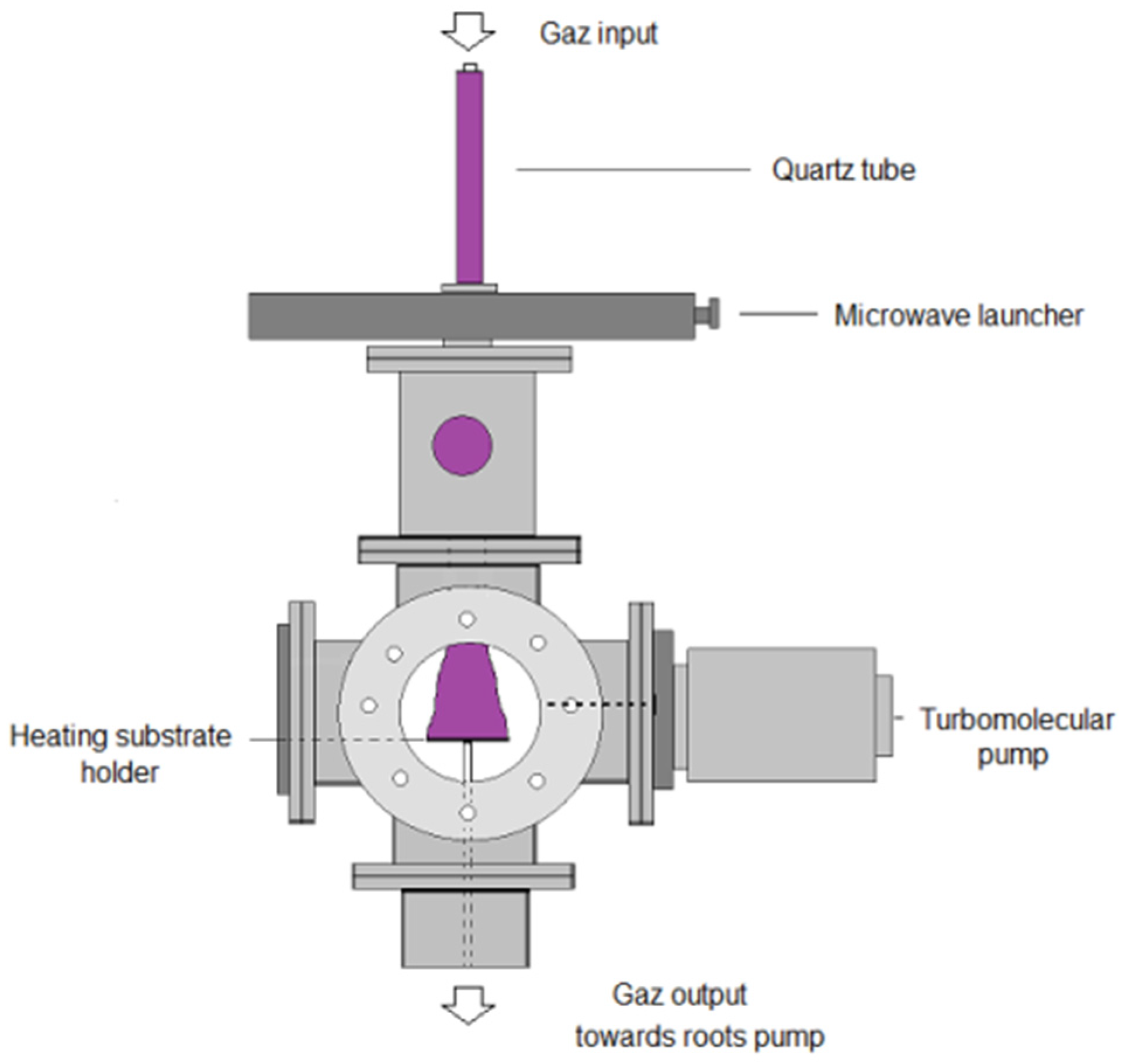
2.2. Expanding Plasma Process

In expanding plasma, the gaseous species such as electrons, ions, neutrals…are produced within the microwave discharge and carried along the discharge up to the surface of the substrate (Figure 1).
The power of the electromagnetic wave of frequency of 2.45 GHz absorbed by the plasma is mainly transferred to the electrons. The conditions of propagation of the electromagnetic wave outside the microwave launcher are satisfied when the density of electrons is above a critical value. In pure Ar gas, the density of electrons is equal to 1.68 × 10¹⁶ m−3 at a microwave power of 400 W and at 2 cm from the discharge tube exit. Under such conditions, the plasma frequency is higher than the microwave frequency. So, the electromagnetic wave is reflected by the plasma. See [26] and references herein for a detailed description of the reactor. Because of inelastic collisions between molecules and electrons, the addition of molecular gases in Ar gas induces a strong decrease of the plasma length due to the decrease of the density of electrons in the plasma. The density of electrons in (Ar-33%N2-1%H2) plasma ranges between 0.03 × 10¹⁶ and 0.15 × 10¹⁶ m3 at 400 W. Since the ion energy at the sheath entrance is equal to about 0.1 eV, the physical sputtering induced by most plasma processes, as well as the heating effect, can be neglected. So, our process promotes chemical reactions as the reduction of oxides and carbides at the surface of the films, which improves the nitrogen transfer into metal films.

2.3. Nitriding Treatments

The titanium substrates of dimensions equal to about 1 cm2 are placed on the heating substrate holder in the plasma reactor. The vacuum chamber is evacuated to a pressure of about 10−4 Pa and the heating is switched on. The substrates are heated at 400, 500, 600 or 800 °C for 30 min. The (Ar-33%N2-1%H2) gas mixture is then introduced at a total pressure of 0.13 kPa and the discharge is produced with a power of about 500 W. The experiments are run for 0.5 h, 1 h, 1.5 h, 3 h or 4 h. Subsequent to nitridation, the substrates are allowed to cool to room temperature in the reactor. Two or three samples prepared under same experimental conditions have been investigated by X-ray diffraction (XRD) to check the reproducibility of results (for example: Ti film, 250 nm thick heated at 600 °C and exposed to plasma for 30 min).

2.4. Investigations of Titanium Silicides and Nitrides

The crystalline structure of as-processed substrates is investigated by X-ray diffraction (XRD, Bruker, Karlsruhe, Germany) and Raman spectroscopy (Horiba-Jobin-Yvon, Villeneuve d’Ascq, France). In addition, Raman spectroscopy can also give information on amorphous and disordered materials because it is quite sensitive to molecule vibrations. The diffusion of nitrogen and silicon into titanium films is identified by secondary ion mass spectrometry (SIMS, CAMECA, Gennevilliers, France). The microstructure of films is characterized by transmission electron microscopy (TEM, JEOL, Tokyo, Japan).

2.4.1. X-ray Diffraction (XRD) Measurements

XRD experiments are conducted using a D8 Advance Bruker diffractometer equipped with a Lynx-eye position sensitive detector (3.4° for fast acquisition). The system works in Bragg-Brentano geometry.

2.4.2. Raman Spectroscopy Experiments

Raman measurements are carried out in backscattering geometry using a Horiba-Jobin-Yvon spectrometer T 64000 model equipped with a CCD camera cooled by a flux of liquid nitrogen up to 140 K in order to reduce the thermal noise. Spectra were excited using an Ar+ laser (514.532 nm) focused onto the sample via a 50×-long working distance objective. The size of the spot is equal to about 1 μm. The power of the laser is adapted to prevent any damage to the sample. All spectra are averaged, so the signal intensities are representative of the treated material.

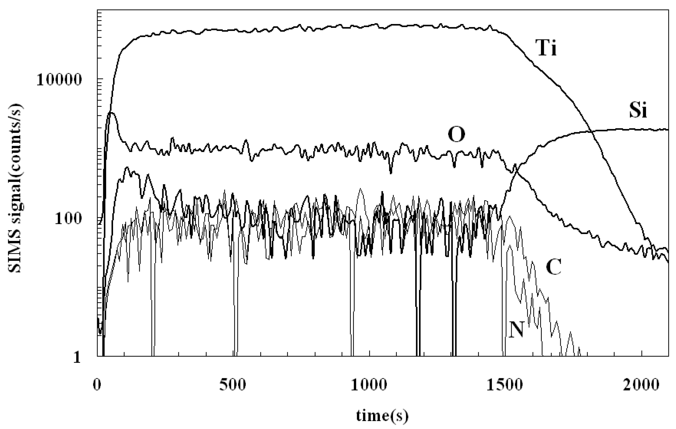
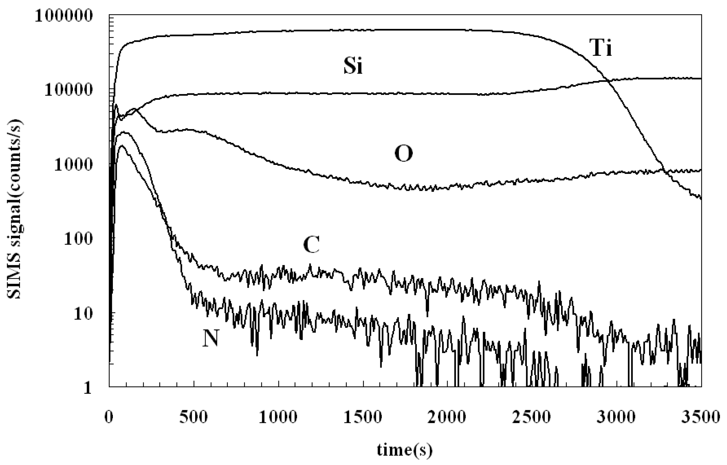
2.4.3. Secondary Ion Mass Spectrometry (SIMS) Investigations

SIMS experiments are conducted in a CAMECA IMS 7F using cesium ions (Cs+) with a primary beam voltage and intensity of 5 kV and 25 nA, respectively. The primary beam is scanned over an area of 200 μm × 200 μm. The results are normalized with respect to the cesium signal.

2.4.4. Transmission Electron Microscopy (TEM)

The microstructure of the as-processed titanium films is investigated by TEM with a JEOL 2100F electron microscope operating at a voltage of 200 kV. Thin films for TEM observations are prepared by mechanical polishing, dimpling and Ar+ ion beam thinning.

3. Results

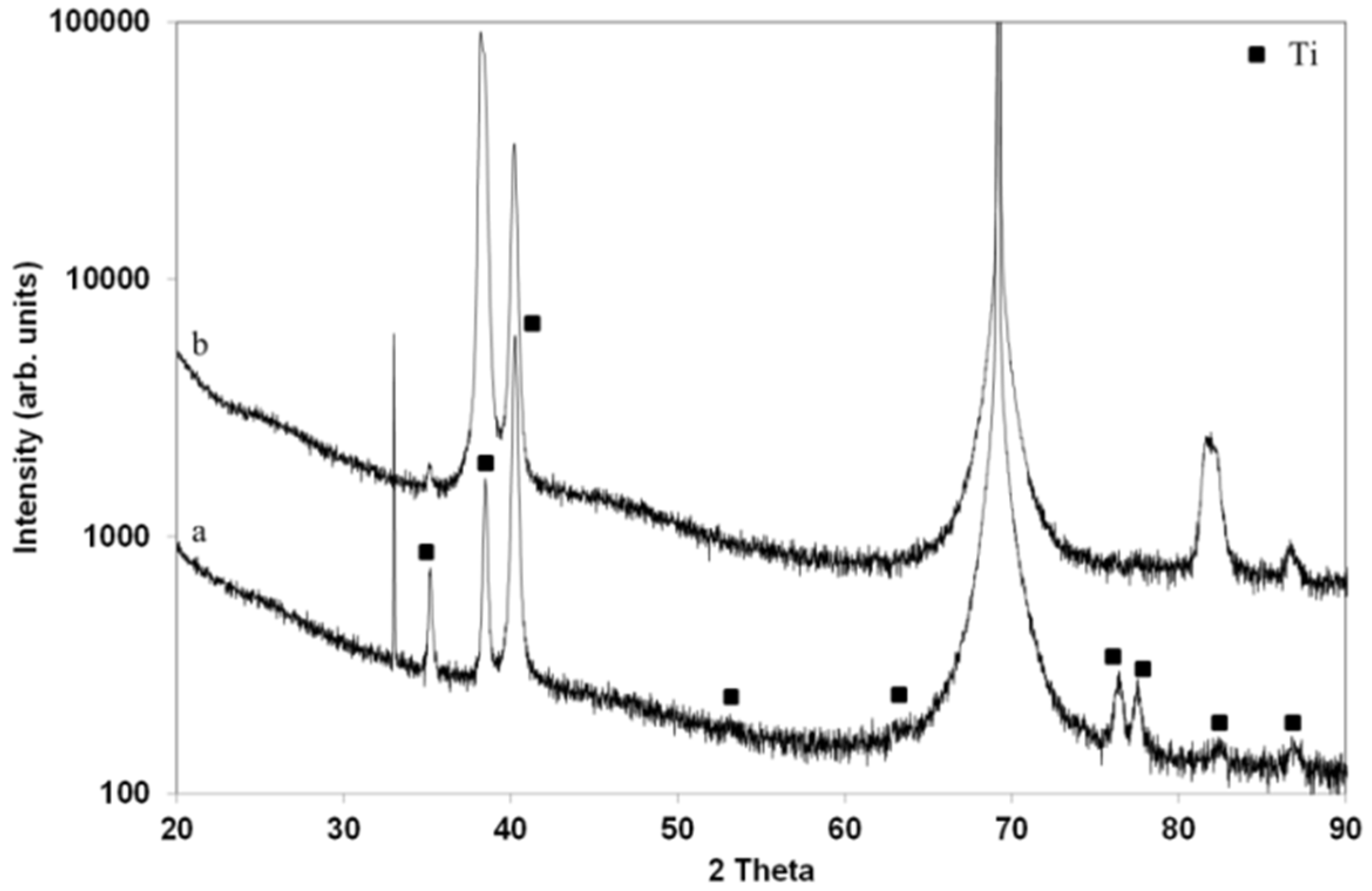
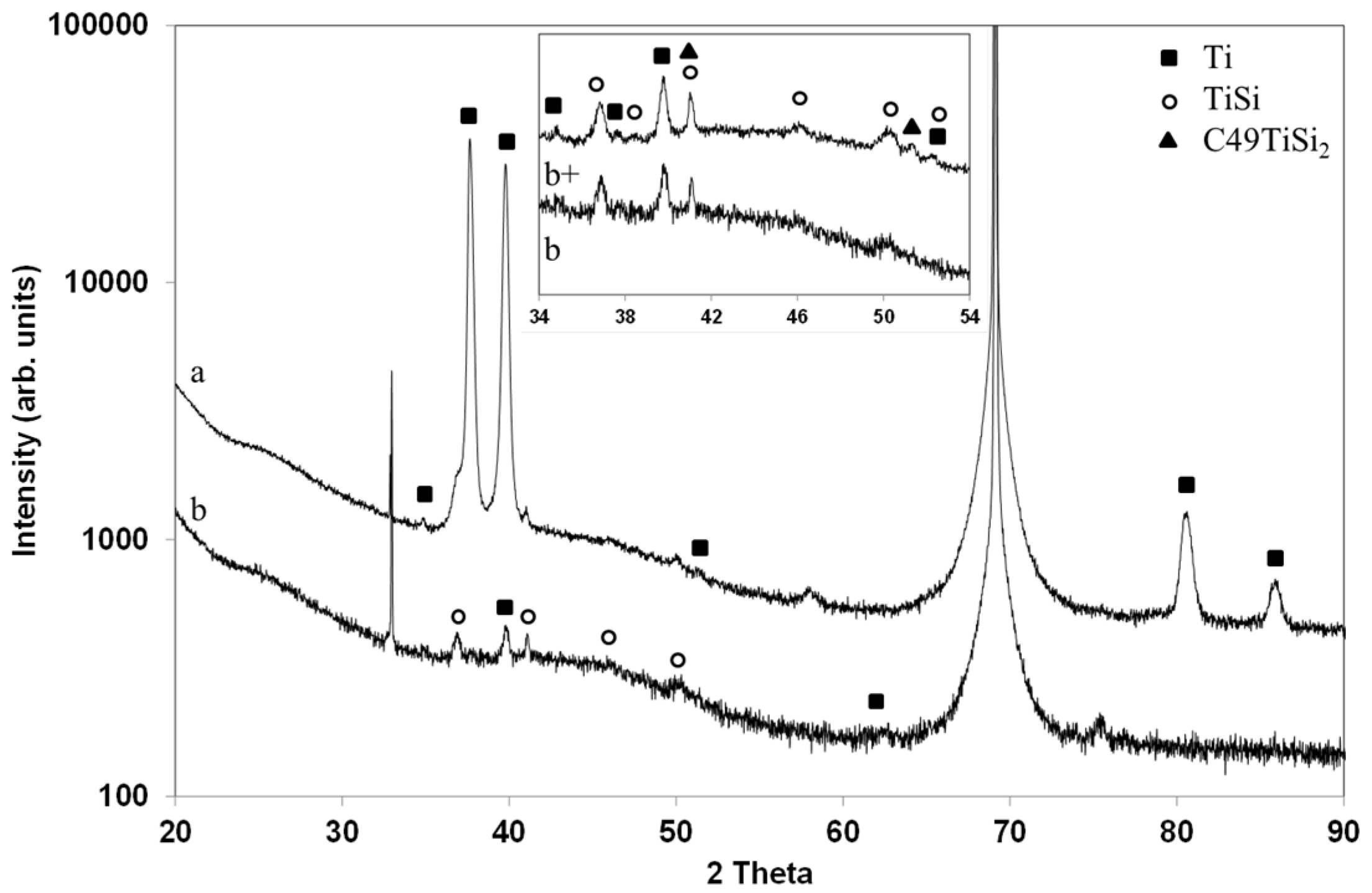
3.1. Crystallization of Ti in As-Deposited Ti Films and Ti Films Processed at 400 °C

Ti crystallizes in the hexagonal structure with the lattice parameters, a = b = 0.29505 and c = 0.46826 nm (JCPDS card no. 00-044-1294) in as-deposited films 250 and 500 nm thick. Except the sharp peaks at Bragg angles 2θ = 69° and 33°, corresponding to the Si substrate (JCPDS card no. 01-7247), all peaks are those of pure Ti metal (Figure 2a). It is worth noting that the peak at 33° corresponds to the forbidden (200) reflection of the Si substrate. More details are given in [27]. No preferential crystalline orientation is detected. However, a 4 h treatment in (Ar-33%N2-1%H2) plasma carried out on Ti films 500 nm thick and heated at 400 °C induces a strong change in diffraction patterns (Figure 2b), since compared with Figure 2a, the (002) diffraction line at 2θ = 38.4° is more intense than the (101) at 2θ = 40.2°. This drastic change is especially identified on the (004) diffraction line at 2θ = 82.3°.
Such a result is probably due to the Si atoms diffusion into the Ti grain boundaries before they diffuse into the Ti crystallites. So, the Si diffusion probably promotes the occurrence of stresses in the structure. SIMS depth profiling is carried out to identify the Ti-Si interface which is the centre of the reaction of the formation of Ti silicides (Figure 3).
The nitrogen and carbon signals remain low in the as-deposited Ti films. However, the high amount of oxygen is probably due to the oxygen diffusion into Ti during the metal evaporation. It is well known that Ti metal strongly reacts with oxygen. The enthalpy of formation of TiO2 at 273 K is equal to −944 kJ·mol−1 compared with the one of TiN, which is equal to −338 kJ·mol−1 [3].

3.2. Crystallization of TiSi and C49TiSi2 in Ti Films Processed at 500 °C

Since the crystallization of metal-rich silicides only starts around temperatures of about 500 °C, the following analysis is focused on the first stages of the formation of titanium silicides in titanium films, 250 and 500 nm thick, heated at 500 °C and exposed to (Ar-33%N2-1%H2) plasma for 1.5 h and 3 h. The same (00l)/(h0l) intensity ratio of Ti crystallites is still observed on XRD pattern (a) in Figure 4.
However, compared with the results obtained at 400 °C, all Ti reflection lines are strongly shifted towards lower Bragg angles. The shift can be related to the Si diffusion into Ti crystallites that leads to an expansion of the metal lattice. The resulting lattice parameters are a = b = 0.297 and c = 0.477 nm. Such a larger (00l) intensity and large shifts of Ti diffraction lines towards lower Bragg angles have also been observed by O. Chaix-Plucherry et al. [18], who conducted very accurate investigations on the formation of silicides in a 100 nm thick Ti-Si system by means of in-situ XRD experiments. The authors report that the Si diffusion into Ti grain boundaries develops a very compressive stress on Ti grains of about 1 GPa. The stress/strain analysis shows that the maximum Si content in Ti grains is closed to 4.5%. The XRD pattern (a) in Figure 4 also displays new, less intense features which are identified as the most intense (210) and (211) diffraction lines of TiSi (JCPDS card no. 00-017-0424) at 2θ equal to about 36.7° and 41°, respectively. The peak at 2θ equal to about 58° is not identified. Longer treatment durations of up to 3 h confirm the simultaneous presence of Ti with expanded lattice and TiSi as well as C49TiSi2 (Figure 4b and especially Figure 4b+ in the inset, obtained from longer counting duration). The XRD diffraction lines correspond to (210), (102), (211), (112), (020) and (311) atomic planes of TiSi located at about 2θ = 36.7°, 38.4°, 41°, 46.2°, 50° and 52.2° respectively as well as (131) and (002) atomic planes of C49TiSi2 at 2θ = 41° and 51.3°, respectively which are the most intense lines of C49TiSi2 (JCPDS card no. 04-002-1352). However, in contrast with the film processed for 1.5 h, the intensity of Ti (101) and (002) lines has strongly decreased. So, these results clearly show that TiSi and C49TiSi2 develop to the detriment of Ti expanded lattice. It is worth noting that the formation of other intermediate silicides such as Ti5Si3 and Ti5Si4 cannot be ruled out because the corresponding more intense reflections overlap those of TiSi [28]. However, Ti5Si3 (JCPDS card no. 04-003-5503) and Ti5Si4 (JCPDS card no. 04-003-1643) show intense diffraction lines around 42.5°–43° where no diffraction line is identified (Figure 4), whereas TiSi is well identified. So, we choose to only keep the TiSi phase.
The strong influence of the thickness of Ti films on the formation of silicides and especially on C49TiSi2 phase is shown in (Figure 5a,b) since, in contrast with the 500 nm thick Ti film, the XRD pattern of the 250 nm thick Ti film processed under the same experimental conditions for 1.5 h only exhibits a broad and slightly intense Ti (101) diffraction line compared with those corresponding to C49TiSi2.
The shift of Ti (101) towards lower Bragg angles has increased, so the (002) diffraction line probably overlaps the most intense TiSi (210) diffraction line. Moreover, the C49TiSi2/TiSi intensity ratio increases with decreasing film thickness. So, the reaction process which occurs in 250 nm thick Ti films progresses further compared with the one occurring in 500 nm thick Ti films. The strong decrease of the intensity of the expanded lattice of Ti is related to the formation of TiSi and C49TiSi2 compounds. Moreover, in contrast with 500 nm thick Ti films, no evolution in the XRD pattern of 250 nm thick Ti films processed for 3 h is identified. So, the kinetics of formation of both compounds tends to be achieved after 1.5 h.

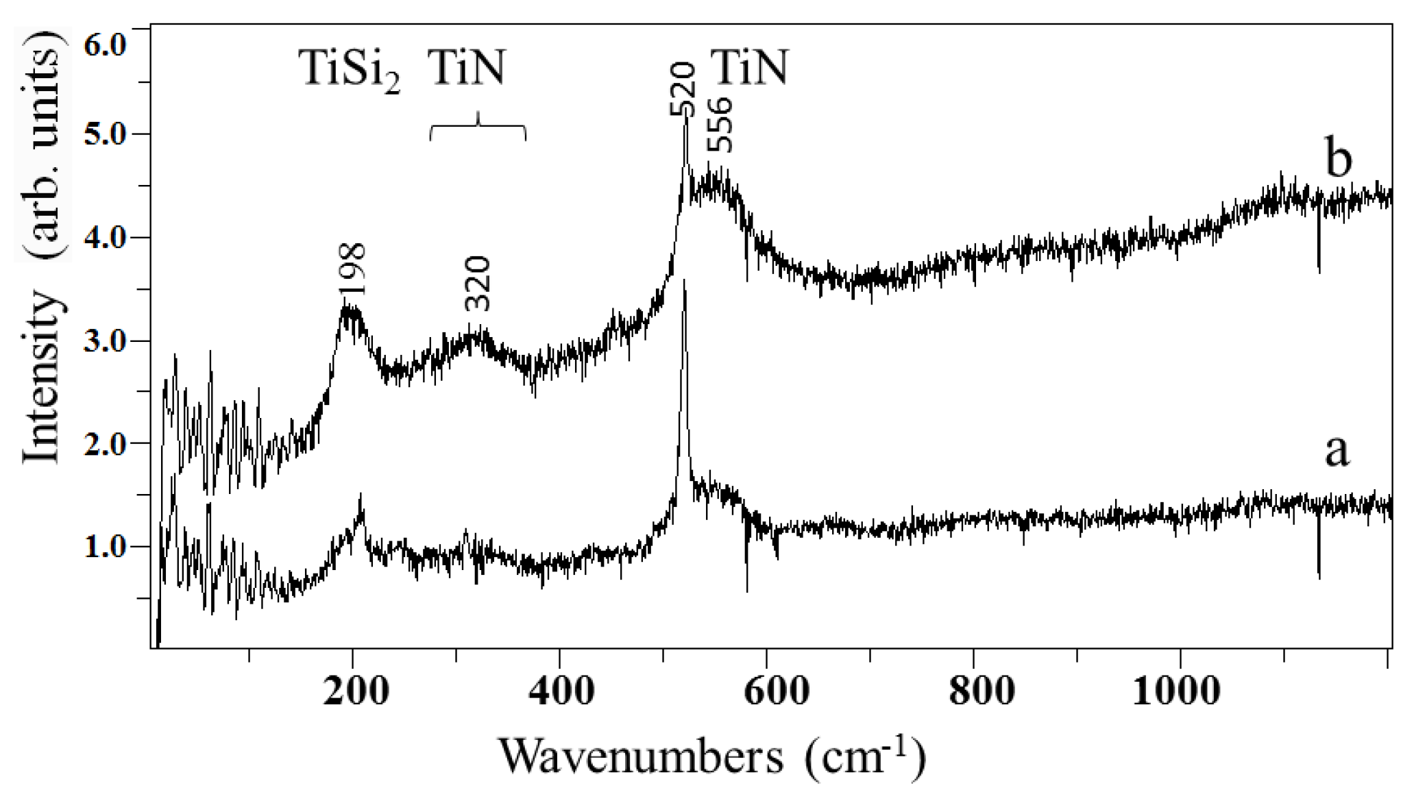
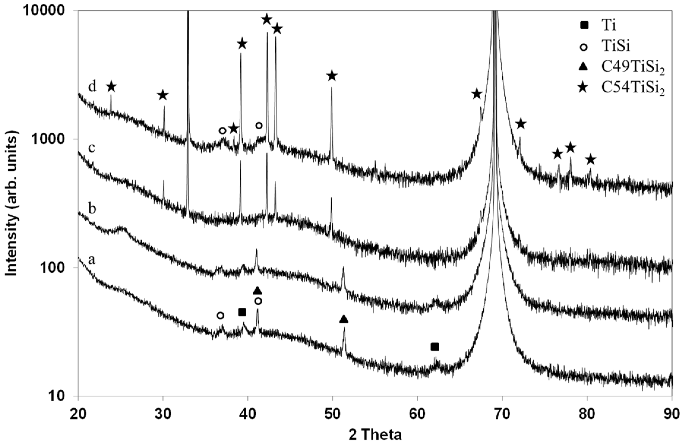
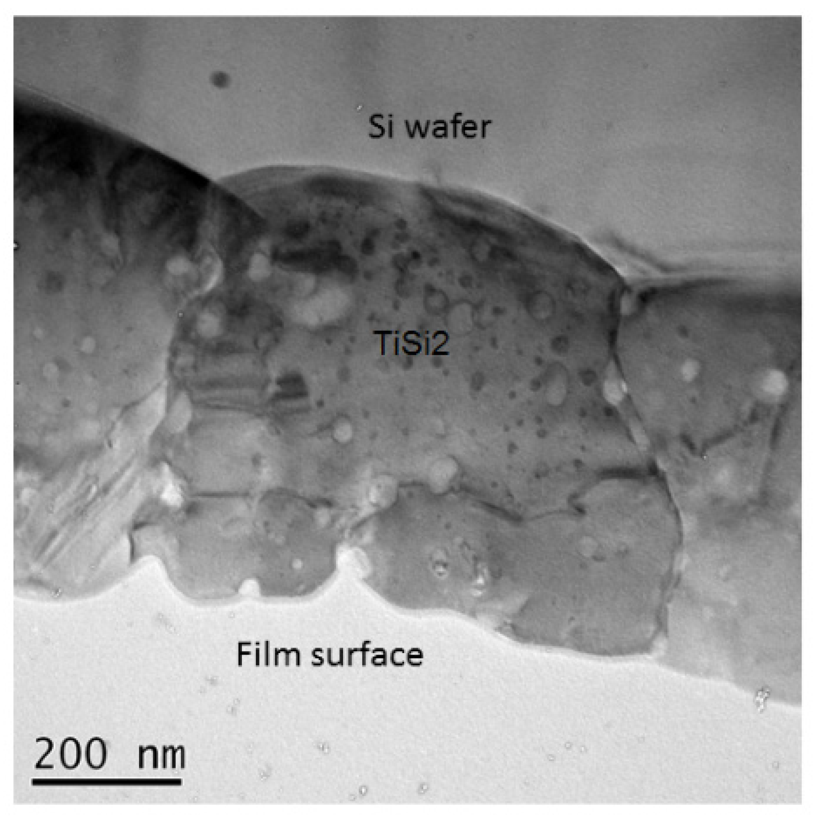
3.3. Crystallization of C54TiSi2 in Ti Films Processed at 600 °C

A 30 min exposure of Ti films, 250 nm thick, heated at 600 °C and processed in (Ar-33%N2-1%H2) plasma leads to the formation of C54TiSi2 (JCPDS card no. 00-035-0785), since the most intense (311), (040), (022) and (331) reflection lines at about 2θ = 39.2°, 42.3°, 43.3° and 49.9°, respectively as well as other lines of lower intensity are clearly identified on the corresponding diffraction pattern (Figure 5c). The reaction of silicidation is very efficient since no pure Ti or any other silicide precursors are detected under such experimental conditions. Jeon et al. [15] report that C54TiSi2 of face-centred orthorhombic structure has the same atomic arrangement in the plane as C49TiSi2 of base-centred orthorhombic structure. The only difference results from different stacking arrangements. See ref. [15] for more details. The film exhibits a (040) preferred orientation. The C54TiSi2 compound also crystallizes in 500 nm thick Ti films (Figure 5d) but in contrast with the previous one, some TiSi remain which are identified as broad peaks of low intensity. Since the diffraction lines are very thin and intense, C54TiSi2 is probably well-crystallized and consists of large grains. These results confirm that the metastable silicide phase of C49 structure would be the main precursor of the stable silicide phase of C54 structure, since it is fully transformed into the C54 silicide at 600 °C.

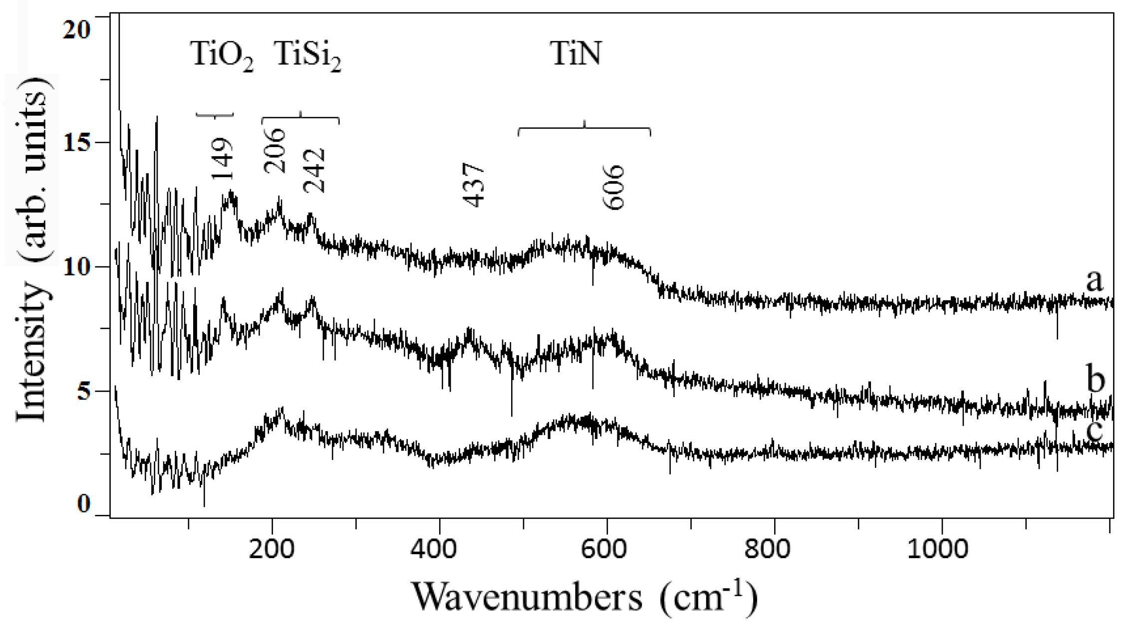
Formation of TiO2 and TiN Compounds

The presence of TiO2 is not clearly displayed on diffraction patterns. However, the most intense diffraction line of TiO2 (anatase phase) is detected at about 2θ = 25° which corresponds to the reflection of the sample holder and so prevents us from identifying a small hump corresponding to an amorphous structure. In contrast with XRD measurements, Raman spectroscopy investigations clearly display the formation of TiO2 oxides in Ti films, 250 nm thick, heated at 600 °C and exposed to (Ar-33%N2-1%H2) plasma for 30 min (Figure 6a).
The anatase and rutile phases of TiO2 are identified. The band at 149 cm−1 corresponds to the most intense lattice vibration of the anatase phase [29]. In the same way, the band located at about 606 cm−1 corresponds to the rutile phase which usually shows the most intense Eg and A1g modes at 446 and 612 cm−1 [30,31]. The other bands of TiO2 of lower intensity are not detected. The spectral signature of Ti metal at about 138 cm−1 is also identified on the spectrum. It consists of a shoulder on the low wave number side of the Raman peak corresponding to TiO2 anatase. In contrast with other metals, Ti exhibits a first order Raman spectrum. It’s TO vibrational mode is Raman active [28]. Concerning Ti silicides formation, the Raman results are quite consistent with the XRD results since the other spectral features located at 187, 206 and 242 cm−1 correspond to the formation of TiSi2 of C54 structure [20]. According to the group theory analysis, the C54 structure exhibits seven Raman active modes, one with A1g character and six with B character [32]. So, the other expected vibrational modes are probably too weak to be detected in our Ti films. In contrast with 250 nm thick Ti films, the intensity of the Raman feature corresponding to the anatase phase is very low on the spectrum recorded from 500 nm thick Ti films and processed under same experimental conditions (Figure 6b). The rutile phase as well as Ti metal and TiSi2 of C54 structure are identified. In general, TiO2 exhibits broader band features than Ti metal and TiSi2, which is indicative of an amorphous rather than a crystalline state. It is worth noting that amorphous or disordered materials have broad Raman features with much weaker peak intensities compared with crystalline structures [28]. In the same way, a thorough examination of the background shows that it seems relatively structured in the wave numbers ranging from 300 to 400 cm−1 and 450 to 600 cm−1. This tendency is confirmed on Raman spectrum (c) in Figure 6 which corresponds to the Ti film heated at 600 °C and exposed to (Ar-33%N2-1%H2) plasma for 3 h. Both regions of the spectrum from 300 to 400 cm−1 and 450 to 600 cm−1 are swelled, especially around 570 cm−1 which corresponds to the most intense optic phonon modes (LO and TO) of TiN lattice vibrations [1,33]. Normally, the high symmetry of B1-structured materials of NaCl-type prevents it from showing a first order Raman spectrum. However, refractory materials such as TiN contain both metal and nitrogen vacancies. The presence of defects reduces the effective symmetry and certain displacements of neighbouring atoms have non-zero first-order polarizability derivatives. These results show that TiN is already formed at 600 °C but because of its amorphous structure, it is not detected on diffraction patterns. TiSi2 is also identified on Raman spectrum (c) in Figure 6. However, the most intense Raman feature of TiO2 is not detected. Since TiO2 is not identified on spectra exhibiting higher amounts of TiN, this result probably highlights the effect of plasma species such as NHx and H which react at the surface of films and reduce oxide compounds. Such an effect has been evidenced during the formation of Mo nitrides [26].

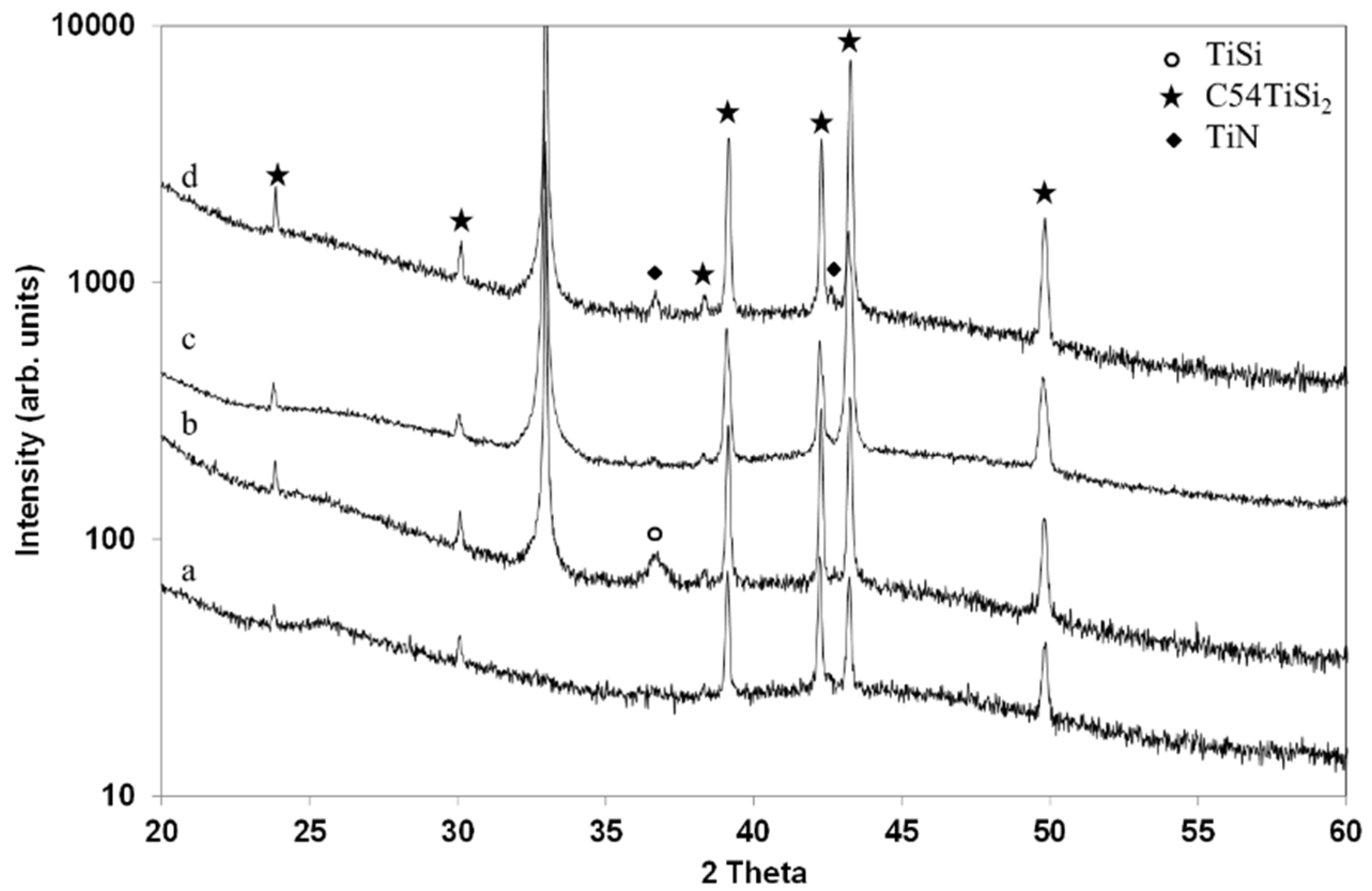
3.4. Crystallization of TiN at 800 °C

The same progress in the kinetics of formation of silicides is also observed at 800 °C since compared with 250 nm thick Ti films, TiSi is still identified in 500 nm thick Ti films heated at 800 °C and exposed to (Ar-33%N2-1%H2) plasma for 30 min (Figure 7a,b).
Moreover, the first signs of TiN with crystalline structure are observed on the diffraction pattern (a) corresponding to the 250 nm thick Ti film. They appear as a tiny shoulder at the higher Bragg angle side of the TiSi2 (040) diffraction line and correspond to the most intense TiN (200) reflection line at about 2θ = 42.6° (JCPDS card no. 04-004-2917). TiSi2 diffraction lines are very thin and intense which confirms a structure with well-crystallized and large grains. In contrast with 250 nm thick Ti films, the 500 nm thick films exhibit a (022) preferred orientation. Longer treatment durations lead to the growth of TiN with crystalline structure (Figure 7c,d). These results are quite consistent with Raman measurements since compared with Ti films processed at 600 °C, the Raman features corresponding to TiN are much thinner, which reflects the formation of an ordered structure. TiSi2 as well as Si at 520 cm−1 are also identified (Figure 8a,b). For the reason previously evoked, TiO2 is reduced by NHx and H species produced in plasma [26].
SIMS depth profiling measurements carried out on Ti films, 500 nm thick, processed in (Ar-33%N2-1%H2) plasma for 1 h show that silicon and nitrogen diffuse widely into the Ti film (Figure 9).
Compared with the as-deposited Ti film (Figure 3), the Ti-Si interface is reached after longer etching times. So, the titanium silicide film is larger than the initial titanium film. Its thickness would be equal to about 800 nm if a constant sputtering rate is assumed. Such a result has been reported in [34]. In this work, 100 nm thick Ti films made by sputtering or evaporation are annealed at 800 °C for 1 h. The resulting thickness of Ti silicide films is equal to 244 nm, which is about twice the initial thickness of the film. The high amount of oxygen in the Ti silicide film is probably due to the increase of the diffusion of oxygen during the plasma process carried out at high substrate temperatures. However, according to Lee et al., in [19] the presence of oxygen in the film could also arise from the native SiO2 at the Ti-Si interface, which reacts with Ti. The authors report that oxygen dissolves into Ti and snow-ploughs ahead of growing Ti silicide films at a relatively low temperature. The structure of 500 nm thick Ti films displayed by the cross-sectional TEM micrograph (Figure 10) mainly consists of large grains about 600 nm across. The grain boundaries are clearly identified, as well as a thin amorphous phase at the metal surface. This phase could correspond to TiN amorphized by the cross-sectional preparation for TEM observations. The result agrees very well with our XRD results and ref. [17,34]. The large grains correspond to C54TiSi2 crystallites and the TiSi2-Si interface is rather smooth.

4. Discussion

4.1. Titanium Silicides

The formation of titanium silicides has been widely discussed in literature. Various compounds can form during the reaction process occurring at the Ti-Si interface. Their composition as well as their sequence depend on the nature of Si substrates (amorphous or crystalline), and on kinetic factors, see ref. [18] for more details.

4.1.1. Formation of TiSi and C49TiSi2

Two main reaction processes have been identified before the metal silicides start to crystallize, see ref. [18] and references herein. The first mechanism leads to the formation of a very thin amorphous or very thin grain silicide layer which grows by means of the diffusion of Si and metal atoms through the Ti-Si interface. Si is reported to be the dominant diffusing species and when saturation occurs, crystallization starts. The second mechanism is a grain boundary diffusion process which has been demonstrated in very thin Ti films, about 2.5 nm thick, coated on Si. In this case, the extensive Ti-Si intermixing leads to a film of composition close to TiSi which consists of very fine grains. Chaix-Pluchery et al. [18] have reported both mechanisms after depositing 100 nm thick Ti films on Si substrates by sputtering, and thermal annealing the as-deposited Ti films. The authors identified the formation of an amorphous layer, 2 nm thick, the diffusion of Si in Ti grain boundaries and grains with the successive formation of alloyed Ti, Ti5Si3 and C49TiSi2 compounds, which coexist in Ti films at temperatures of 400–500 °C, depending on the annealing treatment duration. The second mechanism which is related to the Si diffusion into Ti grain boundaries and grains, the expansion of the Ti lattice, and the formation of TiSi consisting of very fine grains have been observed in our experiments. So, according to our results, TiSi would probably be the main precursor of the C49TiSi2 phase. It is worth noting that Ti5Si3 was identified as a transient phase only existing in a narrow range of temperatures from 412 to 434 °C [18]. In another work, Vishnyakov et al. identified Ti5Si3 (Cx) with dissolved carbon in Ti-Si-C multilayers deposited by magnetron sputtering at 650 °C [35]. The first mechanism, which consists of the formation an amorphous layer at the Ti-Si interface before Ti silicides crystallize, cannot be ruled out. In our work, the Ti films are evaporated on Si substrates heated at 400 °C, which probably promotes the formation of an amorphous layer. Nemanich et al. [31], along with references herein, also identified a strong interdiffusion of Si into 40 nm thick Ti layers during thermal annealing at 400 °C before the silicide is formed. The disordered structures are made out of Si, Ti and O.

4.1.2. Formation of C54TiSi2 Phase

The C54TiSi2 phase is formed from TiSi and C49TiSi2 precursors in Ti films heated at 600 °C and exposed to (Ar-33%N2-1%H2) plasma for 30 min. The reaction is very efficient since no Ti or any precursors are identified in 250 nm thick Ti films. Only some TiSi remains in 500 nm thick Ti films. Since the C49TiSi2 phase does not coexist with the C54TiSi2 phase, C49TiSi2 is probably the main precursor of C54TiSi2. These results are consistent with those reported in [17,34], although the experimental conditions are different: only C54TiSi2 is synthesized in 100–110 nm thick Ti films either sputtered or electron beam evaporated on Si and annealed at 800 °C for 60 min [34]. Both TiSi and C54TiSi2 are present in 100 nm thick Ti films at 675 °C for annealing treatments of 30 s [17], and C54TiSi2 is the only phase obtained at higher temperatures (700–900 °C). However, in other works, C49TiSi2 and C54TiSi2 are simultaneously present in Ti films annealed in N2 ambient at temperatures ranging from 705 to 720 °C for 20–30 s [19], and C49 and C54 silicide phases have been identified in 40 nm thick Ti films annealed at 750 °C for 10 s [20]. So, in contrast with these results, C49TiSi2 is fully transformed into C54TiSi2 in Ti films processed in (Ar-33%N2-1%H2) plasma at 600 °C.

4.2. Formation of TiN Phase

TiN starts to crystallize at 800 °C in Ti films processed in (Ar-33%N2-1%H2) plasma. In contrast with C54TiSi2, the TiN crystallites do not exhibit any preferred orientation. In literature, films of TiN are usually obtained by reactive sputtering in (Ar-N2) gas mixtures [1,3,16,21]. The films exhibit a (111) and (200) orientation at low and high nitrogen content in gas mixtures, respectively [1]. No preferential orientation is observed in TiN films made by pulsed laser irradiation in N2 ambient [23]. Such effects have been observed in Mo2N films since the excess of nitrogen in the structure leads to either crystallites orientation or amorphous structure [36]. Before it crystallizes, the TiN phase with amorphous structure is already formed at 600 °C. Nitrogen species produced in (Ar-N2-H2) plasma react at the surface as well as H species reducing TiO2 compounds. Nitrogen diffuses into the metal film to form TiN while Si and Ti diffuse at the Ti-Si interface to form the titanium silicides. So, both reactions are produced in opposite directions.

4.3. Reaction Process

The results obtained in this work can be described in the light of the three-stage reaction model formulated by S.S. Iyer et al. [14], including the initiation stage, the formation of Ti silicides from the bottom Ti-Si interface and the formation of TiA phase from the Ti surface thermal annealed in ambient gas, and the interaction of the Ti silicides and TiA phases. The reaction process in Ti films exposed to (Ar-N2-H2) plasma, which leads to the formation of silicides and nitrides, is thermodynamically and kinetically controlled and involves the following key stages as follows:
  • The diffusion of Si into grain boundaries and grains of Ti which leads to an expansion of Ti lattice at 400 °C. Simultaneously, the NHx species produced in (Ar-N2-H2) plasma react at the Ti film surface and N diffuses into the metal film.
  • The crystallization and growth of TiSi consisting of very fine grains and C49TiSi2 consisting of larger grains from the bottom interface at 500 °C. TiSi is probably the main precursor of C49TiSi2. TiN of amorphous structure probably start to form in the Ti film.
  • The crystallization of C54TiSi2 at 600 °C, mainly from the C49TiSi2 metastable phase, and the simultaneous growth of TiN of amorphous structure.
  • The crystallization of TiN at 800 °C.

5. Conclusions

Titanium silicides and nitrides have been successfully formed in Ti thin films heated at 400–800 °C and exposed to (Ar-N2-H2) plasma in an expanding microwave plasma reactor. Two competing processes which are thermodynamically and kinetically controlled occur in Ti films: The first is the Si diffusion into Ti grain boundaries and grains at the Ti-Si interface, which leads to the formation of TiSi, C49TiSi2 and finally C54TiSi2 compounds. The formation of other silicides such as Ti5Si3 and Ti5Si4 cannot be ruled out. The metastable C49TiSi2 compound is probably the main precursor of the stable C54TiSi2 compound, which crystallizes at 600 °C. Moreover, the thickness of the film plays a role in the kinetics of formation of silicides. The second process involves the reaction of NHx and H species at the surface of Ti films, which reduce TiO2 and lead to N diffusion into Ti films. TiN of amorphous structure forms, and crystallizes at 800 °C. Further works will be conducted to have a better understanding of both competing processes: the growth of silicides and nitrides, and especially the interaction between them. The role of stresses in the growth of silicides and nitrides in thin films, which leads to preferred orientation of the crystallites, will be also investigated as well as the role of oxygen in the metal film. Moreover, since the diffusion of nitrogen into titanium silicides is expected to improve the electrical properties of TiSix/Si Schottky diodes, electrical conductivity measurements will be performed on Ti films coated on Si substrates and processed in (Ar-N2-H2) expanding microwave plasma.

Acknowledgments

The authors would like to express their gratitude to Thérèse Merle-Méjean for helpful discussions. We gratefully acknowledge the Region Limousin for the support of work on the surface reactivity.

Author Contributions

Isabelle Jauberteau and Jean Louis Jauberteau designed the experiments; Isabelle Jauberteau conceived, performed the experiments, analysed data and wrote the paper; Richard Mayet performed XRD measurements and analyzed data; Julie Cornette performed Raman spectroscopy experiments; Denis Mangin performed SIMS experiments; Annie Bessaudou and Armand Passelergue performed Ti films evaporated on Si wafers; Pierre Carles performed TEM experiments.

Conflicts of Interest

The authors declare no conflict of interest.

References

  1. Ponon, N.K.; Appleby, D.J.R.; Arac, E.; King, P.J.; Ganti, S.; Kwa, K.S.K.; O’Neill, A. Effect of deposition conditions and post deposition anneal on reactively sputtered titanium nitride films. Thin Solid Films 2015, 578, 31–37. [Google Scholar] [CrossRef]
  2. Patsalas, P.; Kalfagiannis, N.; Kassavetis, S. Optical properties and plasmonic performance of titanium nitride. Materials 2015, 8, 3128–3154. [Google Scholar] [CrossRef]
  3. Barhai, P.K.; Kumari, N.; Banerjee, I.; Pabi, S.K.; Mahapatra, S.K. Study of the effect of plasma current density on the formation of titanium nitride and titanium oxynitride thin films prepared by reactive DC magnetron sputtering. Vacuum 2010, 84, 896–901. [Google Scholar] [CrossRef]
  4. White, N.; Campbell, A.L.; Grant, J.T.; Pachter, R.; Eyink, K.; Jakubiak, R.; Martinez, G.; Ramana, C.V. Surface/interface analysis and optical properties of RF sputter-deposited nanocrystalline titanium nitride thin films. Appl. Surf. Sci. 2014, 292, 74–85. [Google Scholar] [CrossRef]
  5. Bailey, E.; Ray, N.M.T.; Hector, A.L.; Crozier, P.; Petuskey, W.T.; McMillan, P.F. Mechanical properties of titanium nitride nanocomposites produced by chemical precursor synthesis followed by high-P,T treatment. Materials 2011, 4, 1747–1762. [Google Scholar] [CrossRef]
  6. Dong, S.; Chen, X.; Gu, L.; Zhou, X.; Xu, H.; Wang, H.; Liu, Z.; Han, P.; Yao, J.; Wang, L.; et al. Facile preparation of mesoporous titanium nitride microspheres for electrochemical energy storage. Appl. Mater. Interfaces 2011, 3, 93–98. [Google Scholar] [CrossRef] [PubMed]
  7. Subramanian, B.; Muraleedharan, C.V.; Ananthakumar, R.; Jayachandran, M. A comparative study of titanium nitride (TiN), titanium oxynitride (TiON), and titanium aluminum nitride (TiAlN) as surface coatings for bio implants. Surf. Coat. Technol. 2011, 205, 5014–5020. [Google Scholar] [CrossRef]
  8. Roquiny, P.; Bodart, F.; Terwagne, G. Colour control of titanium nitride coatings produced by reactive magnetron sputtering at temperature less than 100 °C. Surf. Coat. Technol. 1999, 116, 278–283. [Google Scholar] [CrossRef]
  9. Tsai, J.Y.; Apte, P. A thickness model for the TiSi2/TiN stack in the titanium silicide process module. Thin Solid Films 1995, 270, 589–595. [Google Scholar] [CrossRef]
  10. Guemmaz, M.; Mosser, A.; Parlebas, J.C. Electronic changes induced by vacancies on spectral and elastic properties of titanium carbides and nitrides. J. Electron Spectr. Relat. Phenom. 2000, 107, 91–101. [Google Scholar] [CrossRef]
  11. Griffiths, L.E.; Lee, M.R.; Mount, A.R.; Kondoh, H.; Ohta, T.; Pulham, C.R. Low temperature electrochemical synthesis of titanium nitride. Chem. Comm. 2001, 6, 579–580. [Google Scholar] [CrossRef]
  12. Wriedt, H.A.; Murray, J.L. The N-Ti (nitrogen-titanium) system. Bull. Alloy Phase Diagr. 1987, 8, 378. [Google Scholar] [CrossRef]
  13. Gong, Y.; Tu, R.; Goto, T. Microstructure and preferred orientation of titanium nitride films prepared by laser CVD. Mater. Trans. 2009, 50, 2028–2034. [Google Scholar] [CrossRef]
  14. Iyer, S.S.; Ting, C.Y.; Fryer, P.M. Ambient gas effects on the reaction of titanium with silicon. J. Electrochem. Soc. 1985, 132, 2240–2245. [Google Scholar] [CrossRef]
  15. Jeon, H.; Sukow, C.A.; Honeycutt, J.W.; Rozgonyi, G.A.; Nemanich, R.J. Morphology and phase stability of TiSi2 on Si. J. Appl. Phys. 1992, 71, 4269–4276. [Google Scholar] [CrossRef]
  16. Wang, L.L.; Peng, W.; Jiang, Y.L.; Li, B.Z. Effective Shottky barrier height lowering by TiN capping layer for TiSix/Si power diode. IEEE Electron Device Lett. 2015, 36, 597–599. [Google Scholar] [CrossRef]
  17. Perez-Rigueiro, J.; Herrero, P.; Jimenez, C.; Perez-Casero, R.; Martinez-Duart, J.M. Characterization of the interfaces formed during the silicidation process of Ti films on Si at low and high temperatures. Surf. Interface Anal. 1997, 25, 896–903. [Google Scholar] [CrossRef]
  18. Chaix-Pluchery, O.; Chenevier, B.; Matko, I.; Senateur, J.P.; La Via, F. Investigations of transient phase formation in Ti/Si thin film reaction. J. Appl. Phys. 2004, 96, 361–368. [Google Scholar] [CrossRef]
  19. Lee, W.G.; Lee, J.G. Enhancement of TiSi2 formation during rapid thermal annealing in N2 by the presence of native oxide. J. Electrochem. Soc. 2002, 149, G1–G7. [Google Scholar] [CrossRef]
  20. Satka, A.; Liday, J.; Srnanek, R.; Vincze, A.; Donoval, D.; Kovac, J.; Vesely, M.; Michalka, M. Characterization of titanium disilicide thin films. Microelectron. J. 2006, 37, 1389–1395. [Google Scholar] [CrossRef]
  21. Ohya, S.; Chiaro, B.; Megrant, A.; Neill, C.; Barends, R.; Chen, Y.; Kelly, J.; Low, D.; Mutus, J.; O’Malley, P.J.J.; et al. Room temperature deposition of sputtered TiN films for superconducting coplanar waveguide resonators. Supercond. Sci. Technol. 2014, 27, 015009. [Google Scholar] [CrossRef]
  22. Cabioch, T.; Alkazaz, M.; Beaufort, M.-F.; Nicolai, J.; Eyidi, D.; Eklund, P. Ti2AlN thin films synthesized by annealing of (Ti+Al)/AlN multilayers. J. Mater. Res. Bull. 2016, 80, 58–63. [Google Scholar] [CrossRef]
  23. Wu, J.D.; Wu, C.Z.; Zhong, X.X.; Song, Z.M.; Li, F.M. Surface nitridation of transition metals by pulsed laser irradiation in gaseous nitrogen. Surf. Coat. Technol. 1997, 96, 330–336. [Google Scholar] [CrossRef]
  24. Jauberteau, I.; Merle-Mejean, T.; Touimi, S.; Weber, S.; Bessaudou, A.; Passelergue, A.; Jauberteau, J.L.; Aubreton, J. Expanding microwave plasma process for thin molybdenum films nitriding: Nitrogen diffusion and structure investigations. Surf. Coat. Technol. 2011, 205, S271–S274. [Google Scholar] [CrossRef]
  25. Jauberteau, I.; Jauberteau, J.L.; Touimi, S.; Merle-Mejean, T.; Weber, S.; Bessaudou, A. A thermochemical process using expanding plasma for nitriding thin molybdenum films at low temperature. Engineering 2012, 4, 857–868. [Google Scholar] [CrossRef]
  26. Jauberteau, I.; Mayet, R.; Cornette, J.; Bessaudou, A.; Carles, P.; Jauberteau, J.L.; Merle-Mejean, T. A reduction-nitridation process of molybdenum films in expanding microwave plasma: Crystal structure of molybdenum nitrides. Surf. Coat. Technol. 2015, 270, 77–85. [Google Scholar] [CrossRef]
  27. Zaumseil, P. High resolution characterization of the forbidden Si 200 and Si 222 reflections. J. Appl. Cryst. 2015, 48, 528–532. [Google Scholar] [CrossRef] [PubMed]
  28. Stan, G.E.; Popa, A.C.; Galca, A.C.; Aldica, G.; Ferreira, J.M.F. Strong bonding between sputtered bioglass-ceramicfilms and Ti-substrates implants induced by atomic inter-diffusion post-deposition heat treatment. Appl. Surf. Sci. 2013, 280, 530–538. [Google Scholar] [CrossRef]
  29. Teoh, L.G.; Lee, Y.C.; Chang, Y.S.; Fang, T.H.; Chen, H.Q. Preparation and characterization of nanocrystalline titanium dioxide with a surfactant mediated method. Curr. Nanosci. 2010, 6, 1–5. [Google Scholar] [CrossRef]
  30. Hristova, E.; Arsov, L.I.; Popov, B.N.; White, R.E. Ellipsometric and Raman spectroscopic study of thermally formed films on titanium. J. Electrochem. Soc. 1997, 144, 2318–2323. [Google Scholar] [CrossRef]
  31. Barros, A.D.; Albertin, K.F.; Miyoshi, J.; Doi, I.; Diniz, J.A. Thin titanium oxide films deposited by e-beam evaporation with additional rapid thermal oxidation and annealing for ISFET applications. Microelectron. Eng. 2010, 87, 443–446. [Google Scholar] [CrossRef]
  32. Nemanich, R.J.; Fiordalice, R.W.; Jeon, H. Raman scattering characterization of titanium silicide formation. IEEE J. Quantum Electron. 1989, 25, 997–1002. [Google Scholar] [CrossRef]
  33. Constable, C.P.; Yarwood, J.; Münz, W.D. Raman microscopic studies of PVD hard coatings. Surf. Coat. Technol. 1999, 116, 155–159. [Google Scholar] [CrossRef]
  34. Bhaskaran, M.; Sriram, S.; Short, K.T.; Mitchell, D.R.G.; Holland, A.S.; Reeves, G.K. Characterization of C54 titanium silicide thin films by spectroscopy, microscopy and diffraction. J. Phys. D Appl. Phys. 2007, 40, 5213–5219. [Google Scholar] [CrossRef]
  35. Vishnyakov, V.; Lu, J.; Eklund, P.; Hultman, L.; Colligon, J. Ti3SiC2-formation during Ti-C-Si multilayer deposition by magnetron sputtering at 650 °C. Vacuum 2013, 93, 56–59. [Google Scholar] [CrossRef]
  36. Jauberteau, I.; Bessaudou, A.; Mayet, R.; Cornette, J.; Jauberteau, J.L.; Carles, P.; Merle-Mejean, T. Molybdenum nitride films: Crystal structures, synthesis, mechanical, electrical and some other properties. Coatings 2015, 5, 656–687. [Google Scholar] [CrossRef]
Figure 1. Experimental set-up.
Coatings 07 00023 g001
Figure 2. X-ray diffraction patterns of as-deposited Ti films (a) and Ti films, 500 nm thick, heated at 400 °C and processed in (Ar-33%N2-1%H2) plasma for 4 h (b).
Coatings 07 00023 g002
Figure 3. SIMS depth profiles of as-deposited Ti films.
Coatings 07 00023 g003
Figure 4. X-ray diffraction patterns of Ti films, 500 nm thick, heated at 500 °C and processed in (Ar-33%N2-1%H2) plasma for 1.5 h (a) and 3 h (b).
Coatings 07 00023 g004
Figure 5. X-ray diffraction patterns of Ti films, 250 nm thick, heated at 500 °C and processed in (Ar-33%N2-1%H2) for (a) 1.5 h and (b) 3 h, and Ti films, (c) 250 nm thick, and (d) 500 nm thick heated at 600 °C and processed in (Ar-33%N2-1%H2) for 30 min.
Coatings 07 00023 g005
Figure 6. Raman scattering spectra of Ti films, 250 nm thick (a), and 500 nm thick (b), heated at 600 °C and processed in (Ar-33%N2-1%H2) plasma for 30 min, and Ti films, 500 nm thick (c), heated at 600 °C and processed in (Ar-33%N2-1%H2) plasma for 3 h.
Coatings 07 00023 g006
Figure 7. X-ray patterns of Ti films, 250 nm thick, heated at 800 °C and processed in (Ar-33%N2-1%H2) for 30 min (a), and Ti films, 500 nm thick, heated at 800 °C and processed in (Ar-33%N2-1%H2) for 30 min (b), 1 h (c) and 3 h (d).
Coatings 07 00023 g007
Figure 8. Raman scattering spectra of Ti films, 250 nm thick, heated at 800 °C and processed in (Ar-33%N2-1%H2) plasma for 30 min (a) and 3 h (b).
Coatings 07 00023 g008
Figure 9. SIMS depth profiles of Ti films, 500 nm thick, heated at 800 °C and processed in (Ar-33%N2-1%H2) plasma for 1 h.
Coatings 07 00023 g009
Figure 10. TEM cross-section micrograph of TiSi2 formed from Ti films, 500 nm thick, heated at 800 °C and processed in (Ar-N2-H2) plasma for 1 h.
Coatings 07 00023 g010

