Review

SnS Thin Film Solar Cells: Perspectives and Limitations

1
Laboratory for Applied Physics (LAPS), Department of Computer Science, University of Verona, 37134 Verona, Italy
2
Solid State Chemistry Laboratory, Department of Biotechnology; University of Verona, 37134 Verona, Italy
3
Raman Laboratory, Department of Computer Science, University of Verona, 37134 Verona, Italy
*
Author to whom correspondence should be addressed.
Coatings 2017, 7(2), 34; https://doi.org/10.3390/coatings7020034
Submission received: 27 December 2016 / Revised: 14 February 2017 / Accepted: 16 February 2017 / Published: 22 February 2017
(This article belongs to the Special Issue Thin Film Semiconductors for Photovoltaic Applications)

Abstract

:
Thin film solar cells have reached commercial maturity and extraordinarily high efficiency that make them competitive even with the cheaper Chinese crystalline silicon modules. However, some issues (connected with presence of toxic and/or rare elements) are still limiting their market diffusion. For this reason new thin film materials, such as Cu2ZnSnS4 or SnS, have been introduced so that expensive In and Te, and toxic elements Se and Cd, are substituted, respectively, in CuInGaSe2 and CdTe. To overcome the abundance limitation of Te and In, in recent times new thin film materials, such as Cu2ZnSnS4 or SnS, have been investigated. In this paper we analyze the limitations of SnS deposition in terms of reproducibility and reliability. SnS deposited by thermal evaporation is analyzed by X-ray diffraction, Raman spectroscopy, scanning electron microscopy, and atomic force microscopy. The raw material is also analyzed and a different composition is observed according to the different number of evaporation (runs). The sulfur loss represents one of the major challenges of SnS solar cell technology.

1. Introduction

The limited amount of Te and In in nature, and the toxicity of Cd and Se in CdTe and CuInGaSe2 solar cells, could be overcome with alternative thin film absorbers like Cu2ZnSnS4 or SnS. SnS is a promising “alternative” material due to its electrical and physical properties. Moreover, it has already been proved that a very high quality of SnS layers are required to enhance solar cells efficiency [1]. In order to overcome environmental issues of the typical thin film solar cells and, most importantly, to remove any possible limitations in mass production connected with material scarcity (mainly In and Ga), in 1996 Katagiri et al. [2] introduced a new device with Cu2ZnSnS4 (CZTS) as the absorber layer. This cell has a similar device structure of the Cu(In,Ga)Se2 (CIGS) solar cells [3], but indium and gallium are substituted with the more abundant zinc and tin.
For CZTS, spin coating of precursor solution is one of the most successful techniques, and Todorov et al. [4] demonstrated high efficiency devices by preparing a CZTS solution based on hydrazine. The best cell efficiency was 9.66%, improved by Mitzi et al. up to 10.1% [5] and finally 12.6% by Solar Frontier [6]. However it is possible to prepare the CZTS thin film material with a more industrially-scalable and environmentally-friendly process, such as sputtering [7].
Another most promising “alternative” material is SnS, which has an indirect band gap of 1.0 eV, a direct band gap of 1.3 eV [1,8], and an absorption coefficient exceeding 104 cm−1 [9] in the visible light range [10]. SnS solar cells have a theoretical power conversion efficiency limit higher than 20% [11] and an ideal short circuit current density higher than 30 mA/cm2 [8].
Moreover, due to its simple stoichiometry, different CdTe laboratories have approached it as a possible substitute for CdTe, having in mind that a compound with just two elements would be simpler to control compared to CZTS. However, the latest results reported in the scientific literature shows a different story; solar cells have been fabricated with rather low efficiencies.
SnS forms an orthorhombic crystal structure corresponding to the space group of Pnma [12]where the unit cell consists of double layers stacked onto each other with a weak van der Waals-like coupling along the a-axis, and atoms within the layers are covalently bounded with three neighbors [13]. The defect calculation of this material suggests that the p-type conductivity is due to the easy formation of Sn vacancies (VSn) that act as shallow acceptors [14].
Thin films of SnS for solar cell fabrication have been prepared by different physical deposition methods, such as thermal evaporation [15,16,17,18,19,20], sputtering [21,22,23,24,25], and others [26,27]. Moreover, chemical deposition methods have also been applied, in particular: chemical bath deposition (CBD) [28,29,30,31], electrochemical deposition [32,33], ionic layer adsorption and reaction [34,35], spray pyrolysis method [36,37,38], and atomic layer deposition (ALD) [39,40].
Tin reacts with sulfur forming several binary compounds, including SnS (orthorhombic), SnS2 (trigonal), Sn2S3 (rhombic), Sn3S4 (tetragonal), Sn4S5 [41]. Thus, according to the different preparation conditions, different binary phases can co-exist, influencing the properties of the absorber material. Additionally, changes in composition can result in conductivity type inversion, either p- or n-type [42].
Most of the work done up to now for SnS solar cells has been concentrated in improving the physical and electrical quality of the absorber; a large variety of publications report a wide range of deposition methods, each with different corresponding properties of the material. In the followings some of the most interesting results are reported.
In [43] the fabrication of SnS2/SnS heterojunction thin films diode by plasma enhanced-chemical vapor deposition method is reported: the structure of the cell is glass/TCO/n-type SnS2/p-type SnS/Al, and the best cells performed with an open circuit voltage (Voc) of 0.35 V and a short circuit current density (Jsc) of 1.5 mA/cm2.
Polycrystalline SnS thin films prepared by spray pyrolysis [44] were used to make a solar cell in combination with indium-doped cadmium sulfide as a window layer (p-SnS/n-CdS:In). The best solar power conversion efficiency of 1.3%, with Voc of 260 mV, Jsc of 9.6 mA/cm2, fill factor FF of 53%, was reported.
Ghosh et al. [34] have studied thin film SnS/CdS heterojunctions by thermal evaporation and their junction properties before and after annealing of the window layer with CdCl2 in order to improve its crystallinity with solar power conversion efficiencies of, respectively, 0.05% and 0.08%. The same authors fabricated SnS/CdS structure in a superstrate configuration using CBD CdS followed by SnS deposited by SILAR (successive ionic layer adsorption and reaction) technique [45]. This heterostructure exhibited photovoltaic effect with a Jsc of 52.4 μA/cm2, a Voc of 280 mV and FF of 27%.
In [46] SnxSy thin films prepared by sulfurization of metallic precursors in a nitrogen atmosphere are presented. In any growth conditions, different SnS, Sn2S3, and SnS2 phases were found in the resulting films. Solar cells with a structure of glass/Mo/SnxSy/CdS/ZnO:Ga have performed the following values: Voc =183 mV, Jsc = 2.7 mA/cm2, FF = 34%, and a conversion efficiency of 0.17%. SnS thin films deposited on molybdenum-coated glass substrate by hot wall deposition method and solar cells with a glass/Mo/p-SnS/n-CdS/ZnO structure have been reported with the following performance parameters Voc = 132 mV, Jsc = 3.68 mA/cm2, FF = 29% and with a solar conversion efficiency of 0.5% [47]. Single-phase SnS thin films were prepared by electrodeposition [47] in a sulfur solution containing SnCl2 at high temperature [48]. The first solar cell presented using this deposition technique showed an efficiency of 0.17% [48] (Voc = 155 mV, Jsc = 3.42 mA/cm2 and FF = 31.8%).
Solar cells in a superstrate configuration, with a glass/ZnO:Al/CdS/SnS/Au structure, were prepared via thermal evaporation of both CdS and SnS [1], obtaining a solar power conversion efficiency of 1.6%, which is the highest reported value of devices with thermally-deposited CdS as a buffer layer with a Voc of 208 mV, Jsc of 17.9 mA/cm2, and FF of 38%.
However, it has been reported that CdS is not an ideal compound for SnS solar cells, due to the misalignment of the energy bands with SnS at the junction. For this reason many devices with alternative buffers have been presented. SnS-based solar cells in a superstrate configuration with Zn1−xMgxO (ZMO) as the buffer layer were prepared and the conduction band offset (CBO) was tuned by adjusting the Mg content in the ZMO. Solar cells with the optimum CBO value exhibited a conversion efficiency of 2.1% [49].
SnS thin film solar cells with the structure glass/Mo/SnS/Zn(O,S)/ZnO/ITO were deposited by pulsed chemical vapor deposition (pulsed-CVD) followed by ALD deposition of a Zn(O,S) buffer layer [50]. A certified efficiency of 2.04% was obtained, with Jsc = 19.4 mA/cm2, Voc = 244 mV, and FF = 43.0%. Upon optimization of the SnS absorber and Zn(O,S) buffer, the same group reported an improved cell efficiency of 2.9% [51]. Moreover, by depositing the SnS absorber via ALD and implementing a series of five solar cell optimization steps (aimed at reducing the photo-generated charge carriers’ recombination) the same authors were able to achieve a record efficiency of 4.36% for SnS-based solar cells [10]. A slightly lower efficiency of 3.88% was obtained by the same group by vacuum evaporation [9,52]. A small list of the best efficiencies reported in literature is shown in Table 1.

2. Materials and Deposition Methods

2.1. SnS Deposition

In our laboratory, SnS solar cells were made with the vacuum evaporation (VE) method. Starting from 99.99% pure SnS pieces from Huizhou Tian Yi Rare Material Co. Ltd., Huizhou, China (TRM), SnS thin films were prepared by evaporation with a vacuum pressure below 10−5 mbar and with different substrate temperatures in the range from 250 to 400 °C.
SnS can be deposited in superstrate or substrate configurations, but the best efficiencies were obtained in the substrate configuration where it is possible to separate between absorber deposition and junction formation. Moreover, it is possible to treat the SnS surface prior to the deposition of the buffer layer, as reported in [10]. In our case SnS was deposited in a superstrate configuration on a stack of CdS/ZnO/ITO on soda lime glass. The front contact was made by subsequent radio frequency sputtering deposition of ITO (400 nm) and ZnO (100 nm) layers in an argon/oxygen mixture atmosphere on a previously cleaned soda lime glass substrate heated at 400 °C. Prior to the VE deposition of 200 nm of CdS at 100 °C, the transparent conductive oxide (TCO) was annealed in a vacuum at 450 °C for 30 min. Later, a CdS window layer was annealed in vacuum at 450 °C for 30 min in order to recrystallize CdS grains.

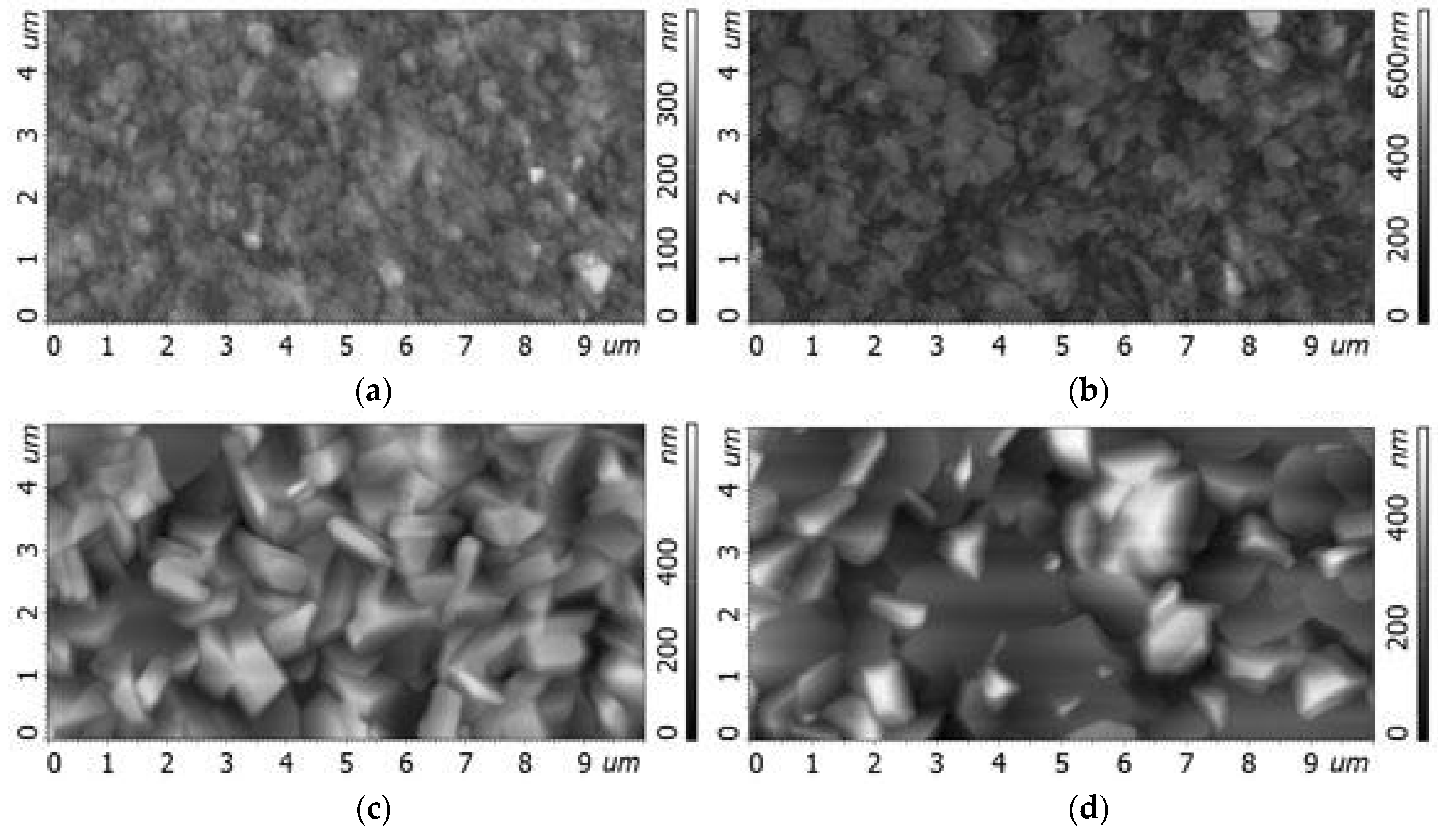
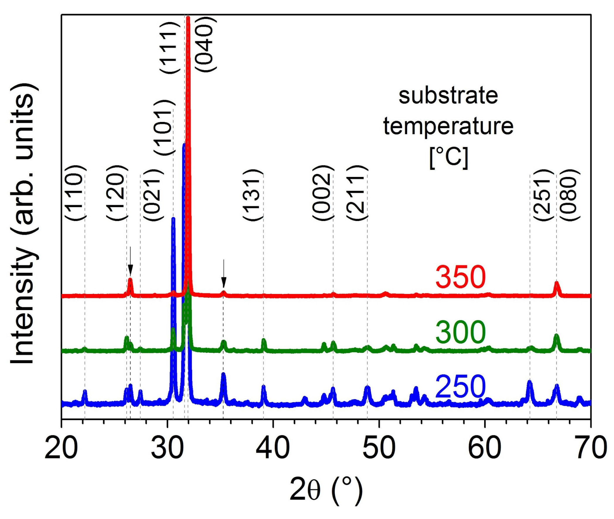
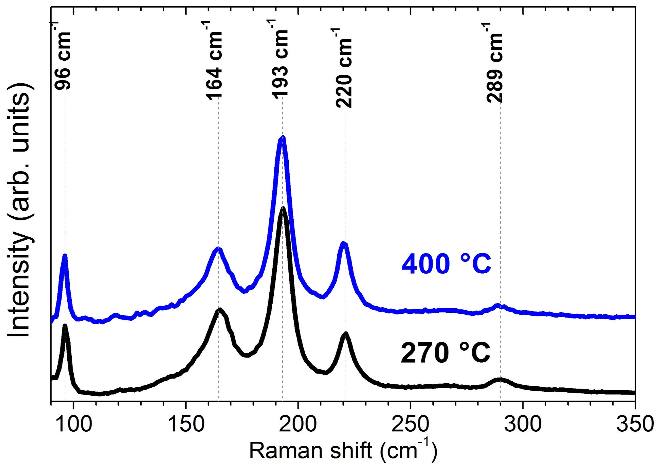
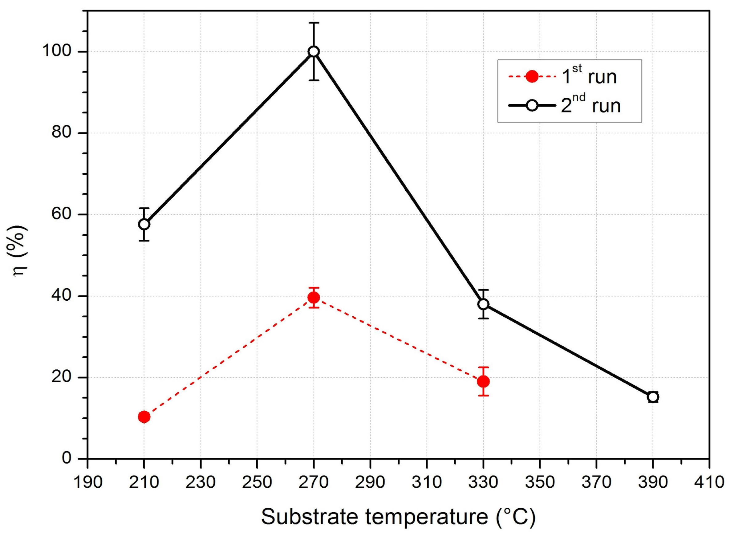
2.2. Substrate Temperature

In Figure 1, the morphology of SnS thin films by atomic force microscopy (AFM) shows to be strongly dependent to the substrate temperature. The SnS thin films’ morphology was studied with a Smena-A AFM microscope (NT-MDT, Moscow, Russia) in semi-contact mode. At a substrate temperature of 200–250 °C the smaller grains are about 0.1 μm in size, with different larger clusters up to 1 μm in diameter. As the substrate temperature is increased from 250 to 350 °C, the grain dimension grows from 102 to 103 nm. At 350 °C the SnS grains showed a very compact morphology: No more flake-like crystal structures were observed, in accordance to what is reported in [8,53].
Figure 2 shows the X-ray diffraction (XRD) patterns of the as-deposited SnS film, the crystalline structure was analyzed with a Thermo ARL X’TRA powder diffractometer (in Bragg-Brentano geometry, equipped with a Cu-anode X-ray source (Kα, λ = 1.5418 Å) and a Peltier Si (Li)-cooled solid state detector, (Thermo Fisher, Waltham, MA, USA). By the comparison between XRD patterns and JCPDS cards, the peaks can be referred to the orthorhombic phase of SnS (Herzenbergite). The patterns were normalized to the (040) peak. The change in grain size and shape seems to be strictly connected to the crystal orientation. A preferred orientation of the grains was observed as the substrate temperature is increased to 300 °C and even more pronounced at 350 °C. In other words, we can observe two main peaks corresponding to the (111) and to the (040) reflections. By increasing the substrate temperature, the (111) peak is reduced and the main peak now corresponds to the (040) reflection. At the highest temperature, the grains are oriented with the crystallographic b axis perpendicular to the sample holder.
The S/Sn ratio has been calculated in order to identify the compound stoichiometry. The elemental analysis was performed with a FEI XL30 scanning electron microscope (SEM, Philips, Amsterdam, Holland) equipped with an energy dispersive X-ray analyzer (EDX). We have registered a slightly Sn rich composition (S/Sn ratio fluctuated between 0.9 and 1.01), demonstrating the potentiality of forming stoichiometric SnS just by directly evaporating the SnS compound, in a way similar to CdTe deposition. However, as already proven [8,54], on the basis of these data we cannot exclude the presence of other phases; for this reason we have also introduced Raman analysis.
Raman spectra of SnS films deposited at substrate temperatures of 270 °C and at 400 °C are shown in Figure 3. They have been collected with a LabRam HR800 microprobe setup (in backscattering geometry) (Horiba Jobin-Yvon, Kyoto, Japan) by using an exciting radiation at 632.8 nm (He-Ne laser). The peak positions are in good agreement with those of SnS single crystal [55], and the absence of any signal in the region just above 300 cm−1 indicates that the layers have no secondary phases. No signals near the wavelength of 310 cm−1 are detected, showing that the SnS thin films do not have secondary phases like Sn2S3 (main mode at 307 cm−1) and SnS2 (312 cm−1) [55].
The effects of the substrate temperature on the crystal structure are only slightly visible in the Raman measurements. The main change between the two spectra is a different relative intensity of the vibrational modes at 164 cm−1 and at 221 cm−1. The most intense peak is at 193 cm−1, which belongs to a symmetric stretching of the Sn-S bond [55] and shows a small shift as the substrate temperature is changed.
At a substrate temperature of 270 °C the 166 cm−1 mode has higher intensity than the one at 221 cm−1, while at a substrate temperature of 400 °C the intensities are inverted. The two modes belong to two different lattice vibrations: Respectively, the interaction along the inter-layer direction and the Sn-S bonding symmetric stretching.

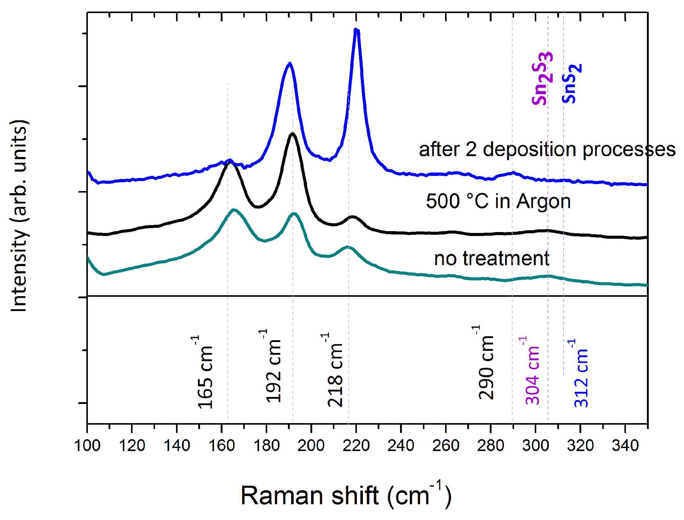
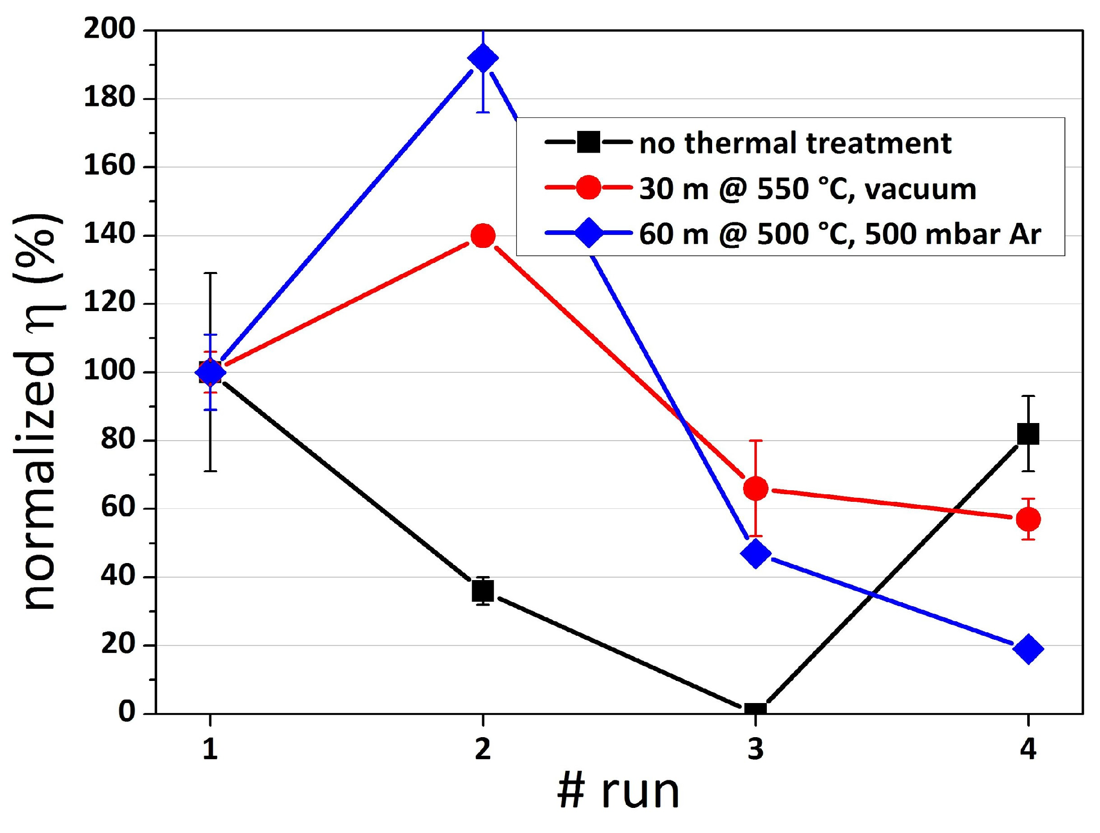
2.3. Evaporation of SnS: Reproducibility

We have observed that the solar cell performance can be connected to the number of times the SnS source is heated. After refilling the crucible, the devices show different performance according to the different runs.
In order to study this phenomenon, we decided to fill the SnS crucible with a large amount of SnS (40 g), in order to allow a large number of following depositions: Substrate temperature, evaporation rate, and absorber layer thickness (2 μm) were constant for each run.
In order to address the possible effects of SnS heating, the material was annealed in two different methods and then analysed:
  • SnS lumps annealing in vacuum in the Knudsen cell at 550 °C for 30 min; and
  • SnS lumps annealing in a quartz tube furnace in controlled atmosphere–Ar at a pressure of 500 mbar at 500 °C for 60 min. A similar thermal treatment of the raw material has been proposed by Steinmann et al. [9] to clean the SnS powders from impurity phases.
In Figure 4 the efficiency (normalized to 100% of the first device) of solar cells made from treated SnS is shown and compared with devices produced with no treatment of the raw material. In this case treating the SnS raw material causes a non-negligible performance improvement produced during the second run. In the subsequent runs the performance decreases.
In Figure 5, XRD analysis of three types of SnS lumps is shown:
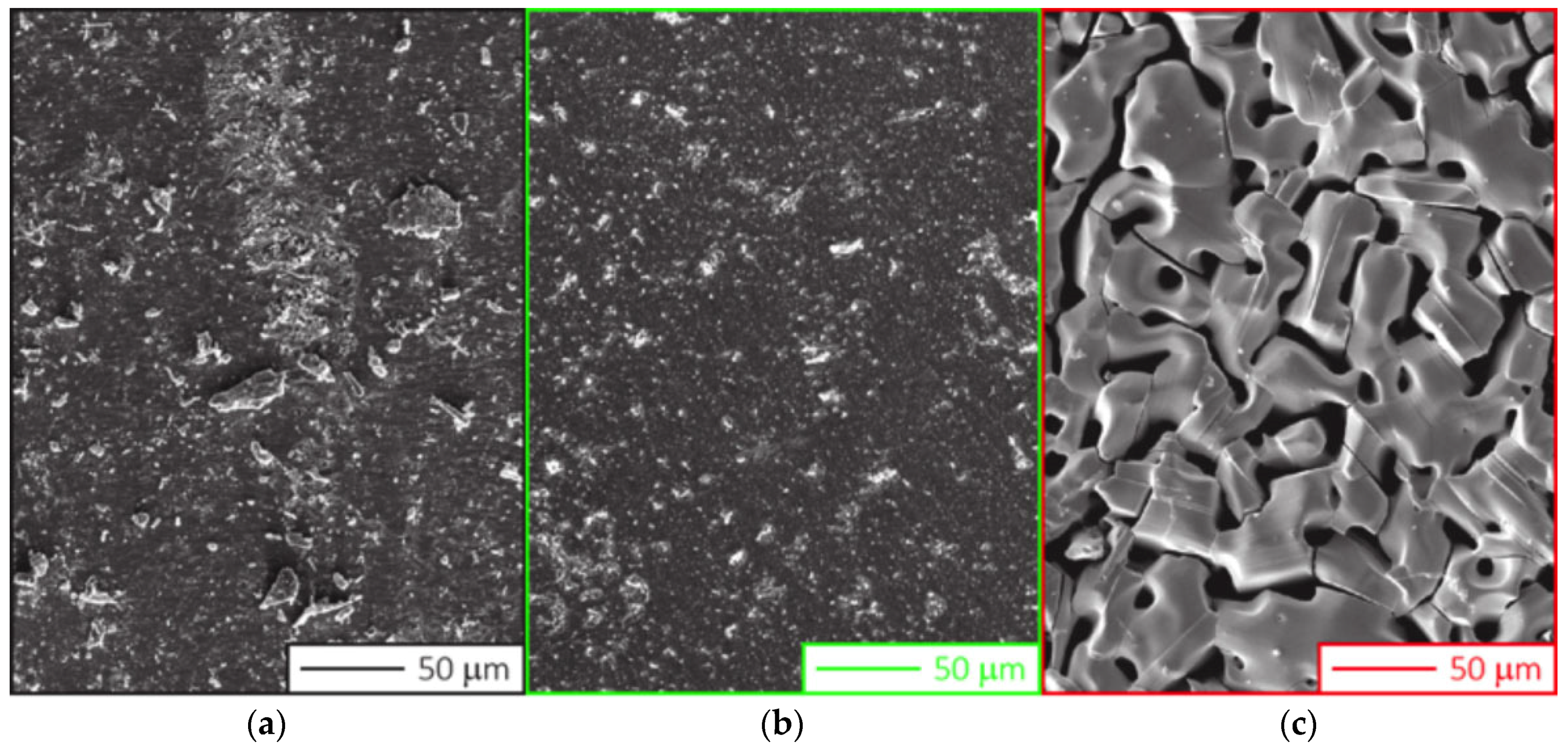
  • TRM SnS as deposited;
  • TRM SnS after 60 min annealing in furnace at 500 °C;
  • TRM SnS after two heating/cooling cycles, i.e., two deposition processes.
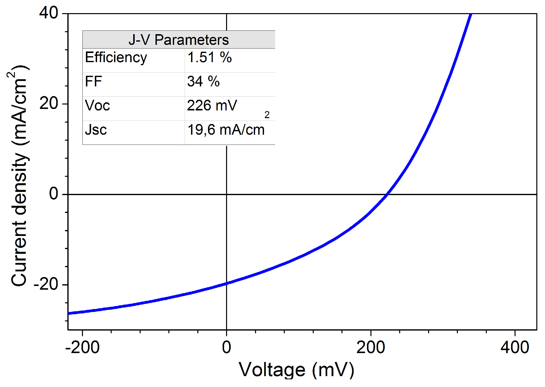
In all the three cases XRD confirmed that the analysed material was orthorhombic SnS. However, the relative intensities of the diffraction peaks were different, this could be explained by the transition that the material experienced: Consisting of a double cycle of sublimation and condensation subdued by SnS.
For a more complete analysis of the SnS evaporation conditions and reproducibility, ≥99.99% pure SnS powders from Sigma-Aldrich Co. LLC. (SA, Saint Louis, MI, USA) have been analysed. The XRD pattern is very similar to the one of the TRM SnS lumps before annealing. However, after annealing the SA material suffered a large modification: a peak of pure SnO2 is observed in the residues, which was not present in the SnS lumps by TRM with the same purity grade. Schneikart [53] has reported that SnS, provided by several suppliers in the form of powders (abcr GmbH & Co. KG, Karlsruhe, Germany; Alfa Aesar, Haverhill, MA, USA; American Elements, Los Angeles, CA, USA), having a strong pressure variation during heating, and that there is a formation of SnS2 film instead of SnS on the substrate before the raw material stabilizes. In this work it was demonstrated that sulphur excess in the samples was due to the presence of SnS2 and SnO2 in the powder of the batch material. Additionally, in our case, we experienced a comparable pressure variation. Although the same SA material has been successfully used by Steinmann et al. [9] in producing the thermally—evaporated record—efficiency solar device (η = 3.88%) (but after annealing of the material).
Many authors reported that XRD measurement is lacking in revealing the presence of SnS2 or Sn2S3 due to the overlapping of the main diffraction peaks of the different phases [39,56]. Again, the Raman technique was applied in order to check the information given from the XRD patterns.
In the first case, i.e., the SnS raw material without treatment from TRM (Figure 5), we observe the main Raman peaks of SnS at Raman energy shifts of 165, 192, 218, and 290 cm−1. Moreover, we observe in some cases the presence of two peaks at 304 cm−1 and at 312 cm−1 which are ascribed, respectively, to the Sn2S3 and SnS2 phases [56]. When SnS material is being treated in the quartz tube furnace at 500 °C (Figure 5), the main SnS peaks are present and only the relative intensity of the peaks are changed. The peak at 192 cm−1 is always more intense than the 165 cm−1 one; this was not observed in the not-treated case described above. The preferential orientation of the sample crystals is then different from the previous case. Additionally, in this case, some of the spectra collected show peaks of Sn2S3 and/or SnS2 phases.
SnS material that underwent the double cycle of sublimation and condensation in the Knudsen cell show, again, all of the SnS Raman peaks. However, a different relative intensity of the peaks appeared: In each spectrum, the peak at 165 cm−1 is weaker compared to the previous cases, whereas the peak at 218 cm−1 is more intense. Moreover, no signal in the region over 300 cm−1 is observed, which indicates the absence of secondary phases showing that the sublimation/condensation cycles have purified the SnS material.
Moreover, the morphology of the samples was analysed by Philips FEI XL30 scanning electron microscopy (SEM), shown in Figure 6. By comparing the non-treated raw material and those treated in the quartz tube furnace at 500 °C, it is possible to say that the treatment seems to have removed the powder from the sample, which is clearly seen in the centre picture of Figure 6. The SEM image in the left of Figure 6 instead demonstrates a transition, as it shows a completely different morphology, which is compatible with SnS sublimation and condensation on a different surface (seen on the top part of the Knudsen cell). This structure is similar to the one of the evaporated SnS when a thin film is deposited at the maximum substrate temperature value before its re-evaporation.
EDX measurements performed on these samples confirm the Raman indications. In Table 2 the calculated S/Sn ratio is summarized. The S/Sn ratio of the non-treated material is about 1.09, which indicates sulphur excess in the raw material. This is compatible with the presence of secondary phases highlighted by Raman spectra. The absence of the Sn2S3 and SnS2 peaks in some of the Raman measurements could suggest that impurity phases are localized in certain areas of the sample. By applying the thermal annealing to the raw SnS, a slight reduction of the S/Sn ratio (1.08) appears. Since this happens together with the SnS powder removal, as observed in Figure 6b, the small particles could be, at least in part, responsible for the sulphur excess. Finally, the S/Sn ratio for the material taken from the Knudsen cell, which experienced the sublimation/condensation double cycle, shows a value close to 1, which is in agreement with the absence of the Sn2S3 and SnS2 peaks in the Raman spectra.
Therefore, we can conclude that the SnS raw material phase purity is a key factor for stoichiometric SnS growth.
It seems that the operation required depositing SnS thin films on the substrates would correct the raw material poor stoichiometry, since the sublimation and the condensation of the material always happen during a deposition process. This could explain the different performance of SnS solar devices due to the thermal history of the raw material, and would suggest that once the raw material is purified, the solar devices would show a better performance.
Moreover, this is consistent with what has been seen by Schneikart [53]: In the first deposition processes SnS2 crystals were grown instead of SnS ones, then, in a successive run, SnS was finally formed. The sulphur excess in the raw material is probably consumed after a certain number of runs. The same authors also reported the formation of a thin (1 nm thick) layer of SnS2 on CdS.

Efficiency

The best efficiency of 1.5% (see Figure 7) was obtained without any post-deposition treatment of SnS, but with deposition after the source material was compacted and prepared by previous annealing. The best efficiency cell has performed the following values: Jsc = 19.64 mA/cm2, Voc = 226 mV, F.F. = 34%, and efficiency = 1.51%.
In Figure 8 efficiencies normalized to the best one corresponding to solar cells made with SnS deposited at different substrate temperatures are shown. Among the different samples, the best performance is achieved at Tsub = 270 °C for samples made in the first run, as well as in the second run. From 210 °C to 270 °C both VOC and JSC increase, however F.F. remains unchanged. Increasing the substrate temperature further, the efficiency drops due to a strong JSC reduction. On the other hand, VOC and F.F. do not change significantly. A similar behaviour is reported for the second run, but with lower efficiencies.
Schneikart et al. [1] reported their best power conversion efficiency η = 1.6% with an optimized substrate temperature of Tsub = 250 °C, while Kawano et al. [8] have achieved their maximum power conversion efficiency of η = 2.53% at Tsub = 200 °C. These results are quite in line with what has been observed in our laboratories.

3. Conclusions

The recent history of SnS research for solar cells has shown that SnS can be deposited with a large variety of deposition methods and with initially promising results. However, in the short-term of the development of the device rather low efficiencies have been obtained. Analysis of SnS deposited by simple evaporation in a vacuum has shown the irreproducibility that many others have also reported. Despite a final efficiency of 1.5% obtained with non-ideal CdS buffer layer, the main process limitation is the strong dependence of sulfur content in the sources, which changes depending on the temperature of previous runs.
This irreproducibility is one of the main limitations to the development of SnS devices and it does not allow concentrating the work on other steps that have to be improved for high efficiency devices, such as an appropriate buffer layer with an optimum alignment of the energy bands, or the reduction of defects. Only when SnS is treated by H2S do devices perform at a reasonable efficiency.
The sulfur loss could be overcome by a specific study of post-deposition treatments, similar to H2S (which is very toxic), able to adjust the final stoichiometry of the absorber without complicating the fabrication process.

Acknowledgments

The “Fondazione Cassa di Risparmio di Trento e Rovereto” with the project TinJet (“bando per progetti di ricerca scientifica finalizzati allo sviluppo di iniziative imprenditoriali”) and the University of Verona with Joint Project 2015 JETTIN are thankfully acknowledged.

Author Contributions

Simone Di Mare designed and performed the experiments; Daniele Menossi and Andrei Salavei designed the deposition machine and contributed to the experiments, Elisa Artegiani prepared the TCO/CdS stacks, Fabio Piccinelli performed and analysed the XRD data, Arun Kumar performed the Raman analysis, Gino Mariotto analysed the Raman data, Alessandro Romeo coordinated all the experiments and wrote the paper.

Conflicts of Interest

The authors declare no conflict of interest. The founding sponsors had no role in the design of the study; in the collection, analyses, or interpretation of data; in the writing of the manuscript, and in the decision to publish the results”.

References

  1. Schneikart, A.; Schimper, H.-J.; Klein, A.; Jaegermann, W. Efficiency limitations of thermally evaporated thin-film SnS solar cells. J. Phys. D Appl. Phys. 2013, 46, 305109. [Google Scholar] [CrossRef]
  2. Katagiri, H.; Jimbo, K.; Maw, W.S.; Oishi, K.; Yamazaki, M.; Araki, H. Development of CZTS-based thin film solar cells. Thin Solid Films 2009, 517, 2455–2460. [Google Scholar] [CrossRef]
  3. Rampino, S.; Armani, N.; Bissoli, F.; Bronzoni, M.; Calestani, D.; Calicchio, M. 15% efficient Cu(In,Ga)Se2 solar cells obtained by low-temperature pulsed electron deposition. Appl. Phys. Lett. 2012, 101, 132107. [Google Scholar] [CrossRef]
  4. Todorov, T.K.; Reuter, K.B.; Mitzi, D.B. High-efficiency solar cell with earth-abundant liquid-processed absorber. Adv. Mater. 2010, 22, 156–159. [Google Scholar] [CrossRef] [PubMed]
  5. Barkhouse, D.A.R.; Gunawan, O.; Gokmen, T.; Todorov, T.K.; Mitzi, D.B. Device characteristics of a 10.1% hydrazine-processed Cu2ZnSn(Se,S)4 solar cell. Prog. Photovolt. Res. Appl. 2012, 20, 6–11. [Google Scholar] [CrossRef]
  6. Wang, W.; Winkler, M.T.; Gunawan, O.; Gokmen, T.; Todorov, T.K.; Zhu, Y. Device characteristics of CZTSSe thin-film solar cells with 12.6% efficiency. Adv. Energy Mater. 2014, 4, 1–5. [Google Scholar] [CrossRef]
  7. Marchionna, S.; Garattini, P.; Le Donne, A.; Acciarri, M.; Tombolato, S.; Binetti, S. Cu2ZnSnS4 solar cells grown by sulphurisation of sputtered metal precursors. Thin Solid Films 2013, 542, 114–118. [Google Scholar] [CrossRef]
  8. Kawano, Y.; Chantana, J.; Minemoto, T. Impact of growth temperature on the properties of SnS film prepared by thermal evaporation and its photovoltaic performance. Curr. Appl. Phys. 2015, 15, 897–901. [Google Scholar] [CrossRef]
  9. Steinmann, V.; Jaramillo, R.; Hartman, K.; Chakraborty, R.; Brandt, R.E.; Poindexter, J.R. 3.88% Efficient tin sulfide solar cells using congruent thermal evaporation. Adv. Mater. 2014, 26, 7488–7492. [Google Scholar] [CrossRef] [PubMed]
  10. Sinsermsuksakul, P.; Sun, L.; Lee, S.W.; Park, H.H.; Kim, S.B.; Yang, C. Overcoming efficiency limitations of SnS-based solar cells. Adv. Energy Mater. 2014, 4, 1400496. [Google Scholar] [CrossRef]
  11. Herzenberg, R. Kolbeckina, un nuevo mineral de estaño—Buenos Aires. Rev. Miner. 1932, 4, 33–35. [Google Scholar]
  12. Ehm, L.; Knorr, K.; Dera, P.; Krimmel, A.; Bouvier, P.; Mezouar, M. Pressure-induced structural phase transition in the IV–VI semiconductor SnS. J. Phys. Condens. Matter. 2004, 16, 3545–3554. [Google Scholar] [CrossRef]
  13. Albers, W.; Haas, C.; van der Maesen, F. The preparation and the electrical and optical properties of SnS crystals. J. Phys. Chem. Solids 1960, 15, 306–310. [Google Scholar] [CrossRef]
  14. Vidal, J.; Lany, S.; D’Avezac, M.; Zunger, A.; Zakutayev, A.; Francis, J. Band-structure, optical properties, and defect physics of the photovoltaic semiconductor SnS. Appl. Phys. Lett. 2012, 100, 032104. [Google Scholar] [CrossRef] [Green Version]
  15. Cheng, S.; Conibeer, G. Physical properties of very thin SnS films deposited by thermal evaporation. Thin Solid Films 2011, 520, 837–841. [Google Scholar] [CrossRef]
  16. Devika, M.; Reddy, N.K.; Ramesh, K.; Ganesam, V.; Gopal, E.S.R.; Ramakrishna, K.T.R. Influence of substrate temperature on surface structure and electrical resistivity of the evaporated tin sulphide films. Appl. Surf. Sci. 2006, 253, 1673–1676. [Google Scholar] [CrossRef]
  17. Devika, M.; Reddy, N.K.; Ramesh, K.; Gopal, E.S.R. Influence of annealing on physical properties of evaporated SnS films. Semicond. Sci. Technol. 2006, 21, 1125. [Google Scholar] [CrossRef]
  18. Devika, M.; Reddy, N.K.; Prashantha, M.; Ramesh, K.; Reddy, S.V.; Hahn, Y.B. The physical properties of SnS films grown on lattice-matched and amorphous substrates. Phys. Status Solidi 2010, 207, 1864–1869. [Google Scholar] [CrossRef]
  19. Hasan, B.A. Dieletectric Properties of Vacuum Evaporated SnS Thin Films. Int. J. Nanotechnol. Adv. Mater. 2013, 1, 87–93. [Google Scholar]
  20. Cheng, S.; Zhong, N.; Huang, C.; Chen, G. SnS films prepared by sulfuration of Sn precursor layers. Adv. Mater. Devices Sens. Imaging II 2005, 5633, 303–307. [Google Scholar]
  21. Hartman, K.; Johnson, J.L.; Bertoni, M.I.; Recht, D.; Aziz, M.J.; Scarpulla, M.A. SnS thin-films by RF sputtering at room temperature. Thin Solid Films 2011, 519, 7421–7424. [Google Scholar] [CrossRef]
  22. Banai, R.E.; Lee, H.; Motyka, M.A.; Chandrasekharan, R.; Podraza, N.J.; Brownson, J.R.S. Optical properties of sputtered SnS thin films for photovoltaic absorbers. IEEE J. Photovolt. 2013, 3, 1084–1089. [Google Scholar] [CrossRef]
  23. Jiang, F.; Shen, H.; Gao, C.; Liu, B.; Lin, L.; Shen, Z. Preparation and properties of SnS film grown by two-stage process. Appl. Surf. Sci. 2011, 257, 4901–4905. [Google Scholar] [CrossRef]
  24. Sousa, M.G.; Da Cunha, A.F.; Fernandes, P.A. Annealing of RF-magnetron sputtered SnS2 precursors as a new route for single phase SnS thin films. J. Alloys Compd. 2014, 592, 80–85. [Google Scholar] [CrossRef]
  25. Reddy, K.T.R.; Reddy, P.P.; Datta, P.K.; Miles, R.W. Formation of polycrystalline SnS layers by a two-step process. Thin Solid Films 2002, 403–404, 116–119. [Google Scholar] [CrossRef]
  26. Tanuševski, A.; Poelman, D. Optical and photoconductive properties of SnS thin films prepared by electron beam evaporation. Sol. Energy Mater. Sol. Cells 2003, 80, 297–303. [Google Scholar] [CrossRef]
  27. Nozaki, H.; Onoda, M.; Sekita, M.; Kosuda, K.; Wada, T. Variation of lattice dimensions in epitaxial SnS films on MgO (001). J. Solid State Chem. 2005, 178, 245–252. [Google Scholar] [CrossRef]
  28. Gao, C.; Shen, H.; Sun, L. Preparation and properties of zinc blende and orthorhombic SnS films by chemical bath deposition. Appl. Surf. Sci. 2011, 257, 6750–6755. [Google Scholar] [CrossRef]
  29. Gao, C.; Shen, H. Influence of the deposition parameters on the properties of orthorhombic SnS films by chemical bath deposition. Thin Solid Films 2012, 520, 3523–3527. [Google Scholar] [CrossRef]
  30. Gode, F.; Guneri, E.; Baglayan, O. Effect of tri-sodium citrate concentration on structural, optical and electrical properties of chemically deposited tin sulfide films. Appl. Surf. Sci. 2014, 318, 227–233. [Google Scholar] [CrossRef]
  31. Jayasree, Y.; Chalapathi, U.; Bhaskar, U.P.; Raja, V.S. Effect of precursor concentration and bath temperature on the growth of chemical bath deposited tin sulphide thin films. Appl. Surf. Sci. 2012, 258, 2732–2740. [Google Scholar] [CrossRef]
  32. Yue, G.H.; Peng, D.L.; Yan, P.X.; Wang, L.S.; Wang, W.; Luo, X.H. Structure and optical properties of SnS thin film prepared by pulse electrodeposition. J. Alloys Compd. 2009, 468, 254–257. [Google Scholar] [CrossRef]
  33. Sato, N.; Ichimura, M.; Arai, E.; Yamazaki, Y. Characterization of electrical properties and photosensitivity of SnS thin films prepared by the electrochemical deposition method. Sol. Energy Mater. Sol. Cells 2005, 85, 153–165. [Google Scholar] [CrossRef]
  34. Ghosh, B.; Das, M.; Banerjee, P.; Das, S. Fabrication of vacuum-evaporated SnS/CdS heterojunction for PV applications. Sol. Energy Mater. Sol. Cells 2008, 92, 1099–1104. [Google Scholar] [CrossRef]
  35. Gao, C.; Shen, H.; Sun, L.; Huang, H.; Lu, L.; Cai, H. Preparation of SnS films with zinc blende structure by successive ionic layer adsorption and reaction method. Mater. Lett. 2010, 64, 2177–2179. [Google Scholar] [CrossRef]
  36. Reddy, K.T.R.; Reddy, P.P.; Miles, R.W.; Datta, P.K. Investigations on SnS films deposited by spray pyrolysis. Opt. Mater. 2001, 17, 295–298. [Google Scholar] [CrossRef]
  37. Sajeesh, T.H.; Warrier, A.R.; Kartha, C.S.; Vijayakumar, K.P. Optimization of parameters of chemical spray pyrolysis technique to get n and p-type layers of SnS. Thin Solid Films 2010, 518, 4370–4374. [Google Scholar] [CrossRef]
  38. Messaoudi, M.; Aida, M.S.; Attaf, N.; Bezzi, T.; Bougdira, J.; Medjahdi, G. Deposition of tin(II) sulfide thin films by ultrasonic spray pyrolysis: Evidence of sulfur exo-diffusion. Mater. Sci. Semicond. Process. 2014, 17, 38–42. [Google Scholar] [CrossRef]
  39. Sinsermsuksakul, P.; Heo, J.; Noh, W.; Hock, A.S.; Gordon, R.G. Atomic Layer Deposition of Tin Monosulfide Thin Films. Adv. Energy Mater. 2011, 1, 1116–1125. [Google Scholar] [CrossRef] [Green Version]
  40. Kim, J.Y.; George, S.M. Tin Monosulfide Thin Films Grown by Atomic Layer Deposition Using Tin 2, 4-Pentanedionate and Hydrogen Sulfide. J. Phys. Chem. 2010, 114, 17597–17603. [Google Scholar] [CrossRef]
  41. Jiang, T.; Ozin, G.A. New directions in tin sulfide materials chemistry. J. Mater. Chem. 1998, 8, 1099–1108. [Google Scholar] [CrossRef]
  42. Ristov, M.; Grozdanov, I.; Mitreski, M. Chemical deposition of TIN (II) sulphide films. Thin Solid Films 1989, 173, 53–58. [Google Scholar] [CrossRef]
  43. Sánchez-Juárez, A.; Tiburcio-Silver, A.; Ortiz, A. Fabrication of SnS2/SnS heterojunction thin film diodes by plasma-enhanced chemical vapor deposition. Thin Solid Films 2005, 480–481, 452–456. [Google Scholar] [CrossRef]
  44. Reddy, K.T.R.; Reddy, N.K.; Miles, R.W. Photovoltaic properties of SnS based solar cells. Sol. Energy Mater. Sol. Cells 2006, 90, 3041–3046. [Google Scholar] [CrossRef]
  45. Ghosh, B.; Das, M.; Banerjee, P.; Das, S. Fabrication and optical properties of SnS thin films by SILAR method. Appl. Surf. Sci. 2008, 254, 6436–6440. [Google Scholar] [CrossRef]
  46. Malaquias, J.; Fernandes, P.A.; Salomé, P.M.P.; Da Cunha, A.F. Assessment of the potential of tin sulphide thin films prepared by sulphurization of metallic precursors as cell absorbers. Thin Solid Films 2011, 519, 7416–7420. [Google Scholar] [CrossRef]
  47. Bashkirov, S.A.; Gremenok, V.F.; Ivanov, V.A.; Lazenka, V.V.; Bente, K. Tin sulfide thin films and Mo/p-SnS/n-CdS/ZnO heterojunctions for photovoltaic applications. Thin Solid Films 2012, 520, 5807–5810. [Google Scholar] [CrossRef]
  48. Steichen, M.; Djemour, R.; Gu, L.; Siebentritt, S.; Dale, P.J. Direct Synthesis of Single-Phase p-Type SnS by Electrodeposition from a Dicyanamide Ionic Liquid at High Temperature for Thin Film Solar Cells. J. Phys. Chem. C 2013, 117, 4383–4393. [Google Scholar] [CrossRef]
  49. Ikuno, T.; Suzuki, R.; Kitazumi, K.; Takahashi, N.; Kato, N.; Higuchi, K. SnS thin film solar cells with Zn1−xMgxO buffer layers. Appl. Phys. Lett. 2013, 102, 193901. [Google Scholar] [CrossRef]
  50. Sinsermsuksakul, P.; Hartman, K.; Kim, S.B.; Heo, J.; Sun, L.; Park, H.H. Enhancing the efficiency of SnS solar cells via band-offset engineering with a zinc oxysulfide buffer layer. Appl. Phys. Lett. 2013, 102, 53901. [Google Scholar] [CrossRef] [Green Version]
  51. Park, H.H.; Heasley, R.; Sun, L.; Steinmann, V.; Jaramillo, R.; Hartman, K. Co-optimization of SnS absorber and Zn(O,S) buffer materials for improved solar cells. Prog. Photovolt. Res. Appl. 2015, 23, 901–908. [Google Scholar] [CrossRef]
  52. Jaramillo, R.; Steinmann, V.; Yang, C.; Hartman, K.; Chakraborty, R.; Poindexter, J.R. Making Record-efficiency SnS Solar Cells by Thermal Evaporation and Atomic Layer Deposition. J. Vis. Exp. 2015, 99, 52705. [Google Scholar] [CrossRef] [PubMed]
  53. Schneikart, A. Herstellung und Charakterisierung von SnS-Dünnschichtsolarzellen. Ph.D. Thesis, Technische Universitat Darmstadt, Darmstadt, Germany, 2014. [Google Scholar]
  54. Noguchi, H.; Setiyadi, A.; Tanamura, H.; Nagatomo, T.; Omoto, O. Characterization of vacuum-evaporated tin sulfide film for solar cell materials. Sol. Energy Mater. Sol. Cells 1994, 35, 325–331. [Google Scholar] [CrossRef]
  55. Chandrasekhar, H.R.; Humphreys, R.G.; Zwick, U.; Cardona, M. Infrared and Raman spectra of the IV-VI compounds SnS and SnSe. Phys. Rev. B 1977, 15, 2177–2183. [Google Scholar] [CrossRef]
  56. Reddy, V.R.M.; Gedi, S.; Park, C.; Miles, R.W.; Reddy, K.T.R. Development of sulphurized SnS thin film solar cells. Curr. Appl. Phys. 2015, 15, 588–598. [Google Scholar] [CrossRef]
  57. Mare, S.D.; Salavei, A.; Piccinelli, F.; Romeo, A. Analysis of SnS Growth and Post Deposition Treatment by Congruent Physical Vapor Deposition. In Proceedings of 31st European Photovoltaic Solar Energy Conference and Exhibition—EU PVSEC 2015, Hamburg, Germany, 14–18 September 2015; pp. 1349–1352.
Figure 1. AFM images of SnS thin films at 200 °C (a), 250 °C (b), 300 °C (c) and 350 °C (d).
Coatings 07 00034 g001
Figure 2. XRD patterns of SnS thin films deposited at different substrate temperatures: 250 °C (blue), 300 °C (green), and 350 °C (red).
Coatings 07 00034 g002
Figure 3. Raman spectra of SnS thin films deposited at 270 °C (black line) and at 400 °C (blue line).
Coatings 07 00034 g003
Figure 4. The normalized efficiency of the solar cells produced from the SnS raw material: untreated (black, square dots), annealed in vacuum (red, circle dots), and annealed in Ar (blue, diamond dots).
Coatings 07 00034 g004
Figure 5. Raman spectra of the SnS raw material, as bought from TRM. The two measurements were carried out on the same sample in different areas.
Coatings 07 00034 g005
Figure 6. SEM scans of the surface of a piece of the (a) as-bought SnS, (b) the raw material after its thermal treatment at 500 °C, and (c) the raw material after two sublimation/condensation cycles.
Coatings 07 00034 g006
Figure 7. IV characteristics of best efficiency SnS solar cells made at a substrate temperature of 250 °C [57].
Coatings 07 00034 g007
Figure 8. Efficiencies of SnS solar cells made with different substrate temperature; first and second runs after refilling of the source.
Coatings 07 00034 g008
Table 1. Summary of main results on SnS solar cells.
SnS DepositionBuffer LayerEfficiencyReference
Spray pyrolysisCdS:In1.3%[44]
Thermal EvaporationCdS1.6%[1]
Thermal EvaporationCdS2.5%[8]
RF-sputteringZn1−xMgxO2.1%[49]
Pulsed-CVDZn(O,S)2.9%[51]
VEZn(O,S)3.88%[9]
ALDZn(O,S)4.36%[10]
Table 2. The S/Sn ratio calculated from EDX measurement.
Material TreatmentS/Sn Ratio
Before treament from TRM1.09
60 m @ 500 °C, 500 mbar1.08
After 2nd deposition1.01

