
An All Sol-Gel Process for the Heteroepitaxial Growth of YBa2Cu3O7−x/LaNiO3/YBa2Cu3O7−x Tri-layer

Department of Materials Physics and Chemistry, Xi’an University of Technology, Xi’an 710048, China
*
Authors to whom correspondence should be addressed.
Coatings 2017, 7(5), 62; https://doi.org/10.3390/coatings7050062
Submission received: 29 March 2017
/
Revised: 18 April 2017
/
Accepted: 24 April 2017
/
Published: 28 April 2017
Abstract
:The preparation of a YBa2Cu3O7−x/LaNiO3/YBa2Cu3O7−x sandwich structured film on a LaAlO3 (100) substrate by a sol-gel method was investigated. YBa2Cu3O7−x/LaNiO3/YBa2Cu3O7−x tri-layer heterostructures with different epitaxial characteristics can be deposited by controlling the heat treatment temperature. X-ray diffraction and transmission electron microscopy results show that the bottom YBCO film grows epitaxially on the LaAlO3 substrate along the c axis, and that this epitaxial growth trend is extended to the subsequently deposited LaNiO3 film. For this reason, the LaNiO3 film also grows epitaxially along the c axis. Furthermore, this epitaxial growth trend is extended to the top YBa2Cu3O7−x film, yielding YBa2Cu3O7−x/LaNiO3/YBa2Cu3O7−x tri-layer heterostructures with epitaxial growth characteristics along the c axis, which enables both the bottom and top YBa2Cu3O7−x layers to possess superconducting abilities.
1. Introduction
The traditional Josephson junction is composed of a sandwich structured superconductor, insulator and superconductor (SIS); this junction requires the thickness of the insulating layer to be similar to the coherence length of the superconducting layers. The coherence length is rather short in high-temperature oxide superconductors, such as YBa2Cu3O7−x (YBCO), which has a length of ξc ~0.1 nm in the c-axis direction and ξab ~2 nm in the a- and b-axis direction direction. It is challenging to acquire uniform and compact insulation layers that are so thin. However, if the middle I (insulator) layer is replaced by an N (normal) layer with metallic conductivity (i.e., superconductor normal superconductor (SNS) structure), the superconducting electron pair, due to the large proximity effect at the interface of a high-temperature superconductor and a conducting layer [1], can pass through the N layer with a thickness of more than 10 nm, which is much farther than the coherence length of the superconductor. Accordingly, the SNS structure can be deposited more easily, and various SNS structures have been developed, such as YBCO/La2−xSrxCuO4 (20 nm)/YBCO [2], YBCO/CaRuO3 (10–50 nm)/YBCO [3] and YBCO/Nb-doped SrTiO3 (25 nm)/YBCO [4]. The Josephson Effect occurs in these structures. Consequently, studies concerning SNS sandwich structures are considered significant for the preparation of Josephson junctions.
LaNiO3, a reported normal conducting N material, is a metallic perovskite structure oxide with a pseudocubic lattice constant (a) of 0.383 nm. Because there is only a small degree of mismatch between LaNiO3 and YBCO (1% in the a-axis direction and 0.7% in the b-axis direction), it is possible to form coherent interfaces at both LaNiO3/YBCO and YBCO/LaNiO3. Moreover, as LaNiO3 contains only two metallic elements, the stability of its structure can be maintained more easily than multi-element structures. As Ni and La both possess +3 metal ion valence states, these two elements are less likely to diffuse into YBCO than are Sr and Ca [5]. Additionally, the carrier concentration and room temperature resistivity of LaNiO3 are close to those of YBCO, such that an ohmic contact can be easily established between YBCO and LaNiO3 [6]. Therefore, LaNiO3 can prospectively be applied as the N material in the SNS sandwiched structure. In earlier work, Sagoi, M. successfully deposited a YBCO/LaNiO3/Au/Ag/Pb structure [7], but its top electrode did not demonstrate high-temperature superconducting properties. Thus, the large proximity effect was not observed. Shortly after, Hegde, M.S. deposited a symmetrical structure of YBCO/LaNiO3/YBCO [8], but details of the epitaxial growth characteristics of the layers and the growth status of the interfaces were not clear.
In addition, the reported epitaxial technologies for growing both SIS and SNS junctions always involved a vacuum environment, which is a major obstacle for large-scale, low-cost productions. In terms of practical application, the sol-gel method for the preparation of SNS junctions is promising because of its low cost and scalability. Recently, significant advances have been made in growing both YBCO and textured oxide films using the sol-gel method [9,10]. However, heteroepitaxial growth on YBCO/LaNiO3/YBCO tri-layers remains challenging, since a sharp interface between YBCO and LaNiO3 films is not easy to obtain at a high temperature of approximately 800 °C, which is the typical temperature for the heat treatment of YBCO films in the sol-gel route [9,11].
In this paper, the feasibility of depositing a YBCO/LaNiO3/YBCO sandwich structure using a sol-gel method is discussed, and its epitaxial growth characteristics and interface characteristic are studied.
2. Experiments
The process for preparing YBCO and LaNiO3 films can be found elsewhere [12,13]. Starting from these previous reports, the solution and heat treatment temperatures were slightly modified to prepare the YBCO/LaNiO3/YBCO tri-layer.
The YBCO solution can be obtained by using yttrium, barium and copper acetates as raw materials; trifluoroacetic acid and acrylic acid as additives; and absolute methanol as the solvent. In this YBCO solution, the pH value is approximately 7, which is neutral. To prepare the LaNiO3 solution, nickel acetate and lanthanum nitrate hexahydrate are used as raw materials, acrylic acid is used as the additive and ethylene glycol monomethyl ether is used as the solvent. The LaNiO3 solution has a weakly acidic pH value of 5–6. To avoid film corrosion caused by the acidic LaNiO3 solution during the dip-coating process, ethanolamine is added to the LaNiO3 solution to adjust the pH value to 7.
Next, each layer in the YBCO/LaNiO3/YBCO tri-layer is coated with gel and then pyrolysis is performed, followed by a heating treatment at a certain peak temperature. The gel coating and pyrolysis processes can be found in references [12] and [13]. The heat treatment temperature is a key factor in preparing the tri-layer. To avoid possible inter-diffusion between the YBCO and LaNiO3 films, a method to decrease the heat treatment temperature layer-by-layer was adopted. For the bottom YBCO film, the surface of the film is more compact and the superconductivity of the film is more favourable (Tc > 91 K, Jc > 1 MA/cm2) when a high heat treatment temperature is used (near 800 °C). The heat stability is particularly better reflected by the bottom film after the thermal shock in the follow-up film deposition process. Therefore, 800 °C was selected as the heat treatment temperature for the bottom YBCO film.
Our previous studies have shown that the LaNiO3 film is in a single phase at the heat treatment temperature of 750 °C. Accordingly, its crystallization quality is favourable, and its specific resistance is comparatively lower [13]. If the heat treatment for the LaNiO3 film is performed at an overly high temperature, the LaNiO3 can be decompounded, which would exert a negative impact on the follow-up epitaxial growth of the film. Therefore, the heat treatment temperature was selected to be 750 °C. However, it is crucial that the deposition of LaNiO3 on YBCO occurs under a low oxygen partial pressure PO2 of 2000 Pa diluted by nitrogen; otherwise, the YBCO (chemical formula of YBa2Cu3O7−x) of the bottom film will become YBa2Cu4O8 [14], and the superconductivity will be affected.
Finally, the top YBCO film is deposited on the LaNiO3/YBCO bilayer. According to references [15] and [16], the heat treatment temperature of the YBCO film can be varied over the range of 700–800 °C by adjusting the oxygen partial pressure. By decreasing the heat treatment temperature layer-by-layer, a comparison study was conducted at three YBCO heat treatment temperatures, 700 °C (with PO2 of 17 Pa), 725 °C (with PO2 of 30 Pa) and 740 °C (with PO2 of 40 Pa) (all below 750 °C, the treatment temperature of the middle LaNiO3 layer) [16].
To directly clarify the different results attained using the three heat treatment temperatures, temperature combinations of 700/750/800 °C, 725/750/800 °C and 740/750/800 °C (named sample A, sample B and sample C, respectively) were compared.
3. Results and Discussion
X-ray diffraction studies were performed to analyse the epitaxial growth characteristics of the layers. The θ–2θ, ω and ϕ scans of sample A are shown in Figure 1a–c; the θ–2θ, ω and ϕ scans of sample B are shown in Figures 1d–f; and the θ–2θ, ω and ϕ scans of sample C are shown in Figure 1g–i, respectively. For sample A (700 °C for the top film), the YBCO (00l) diffraction peak is relatively weak in the θ–2θ scan, and the non-c-axis-oriented YBCO (103) diffraction peak appears at 2θ of 32.8°. In the corresponding ω scan (Figure 1b), the full width at half maximum (FWHM) is relatively large (1.9°). In the corresponding ϕ scan (Figure 1c), two wide diffraction peaks with a width of 100° appear. Therefore, the YBCO film in sample A prefers the c-axis orientation (out-of-plane texture), but high-angle boundaries exist in the ab plane (embodying the worse in-plane texture). This result demonstrates that the given heat treatment temperature is too low, working against the formation of the tri-layer biaxial structure. However, given our previous studies, a YBCO film with favourable superconductivity can still be deposited at 700 °C on a LaAlO3 single-crystal substrate with a lower FWHM value of the diffraction peak of approximately 1°. Clearly, this lower FWHM is due to the difference in the nucleation free energy on the surfaces of the substrates [17].
For sample B, where the heat treatment temperature is increased to 725 °C for the top YBCO film, the YBCO (00l) diffraction peak becomes apparent, and the YBCO (103) diffraction peak disappears in the θ–2θ scan, which indicates that sample B prefers the c-axis orientation. In the corresponding ω scan, the FWHM is 1.45°, which is less than the FWHM of sample A. In the corresponding ϕ scan, diffraction peaks appear at an interval of 90° in the 360° scanned area. If the first peak corresponds to the (019) crystal plane, the following three diffraction peaks would correspond to the (09), (09) and (109) crystal planes, respectively, which is originally due to the four-fold rotation symmetry of the cubic system and indicates that the crystalline grain carries certain in-plane texture in the ab plane. However, the four diffraction peaks differ greatly in intensity, indicating that the in-plane texture of the film is not excellent.
To deposit tri-layers with better in-plane texture, the final heat treatment temperature is further increased to 740 °C (in sample C). In the θ–2θ scan, the YBCO (00l) diffraction peak becomes very sharp, indicating that the YBCO grain is arranged more orderly in the c-axis orientation. In the corresponding ω scan, the FWHM value is 1.45°, the smallest value among the three samples, indicating that sample C has the strongest c-axis preferred orientation. In the corresponding φ scan, a diffraction peak appears every 90°, and the four diffraction peaks have similar peak intensities, which demonstrates that the YBCO film has a better in-plane texture. From the X-ray diffraction analysis results, sample C (740 °C treated top film) has the best biaxial texture.
Through the XRD analysis, it can be generally presumed that the deposited YBCO/LaNiO3/YBCO (sample C) has epitaxial growth characteristics. To deepen the understanding of the growth characteristics of the tri-layer interfaces, cross-section TEM analysis is conducted for sample C. Figure 2 consists of a TEM image of the YBCO/LaNiO3/YBCO tri-layer structure, in which the layers can be clearly distinguished. The TEM image shows that the bottom YBCO film, middle LaNiO3 film and top YBCO film have thicknesses of 128, 187 and 131 nm, respectively. The arrows mark the interfaces between the layers. Overall, the interfaces are smooth, flat and straight.
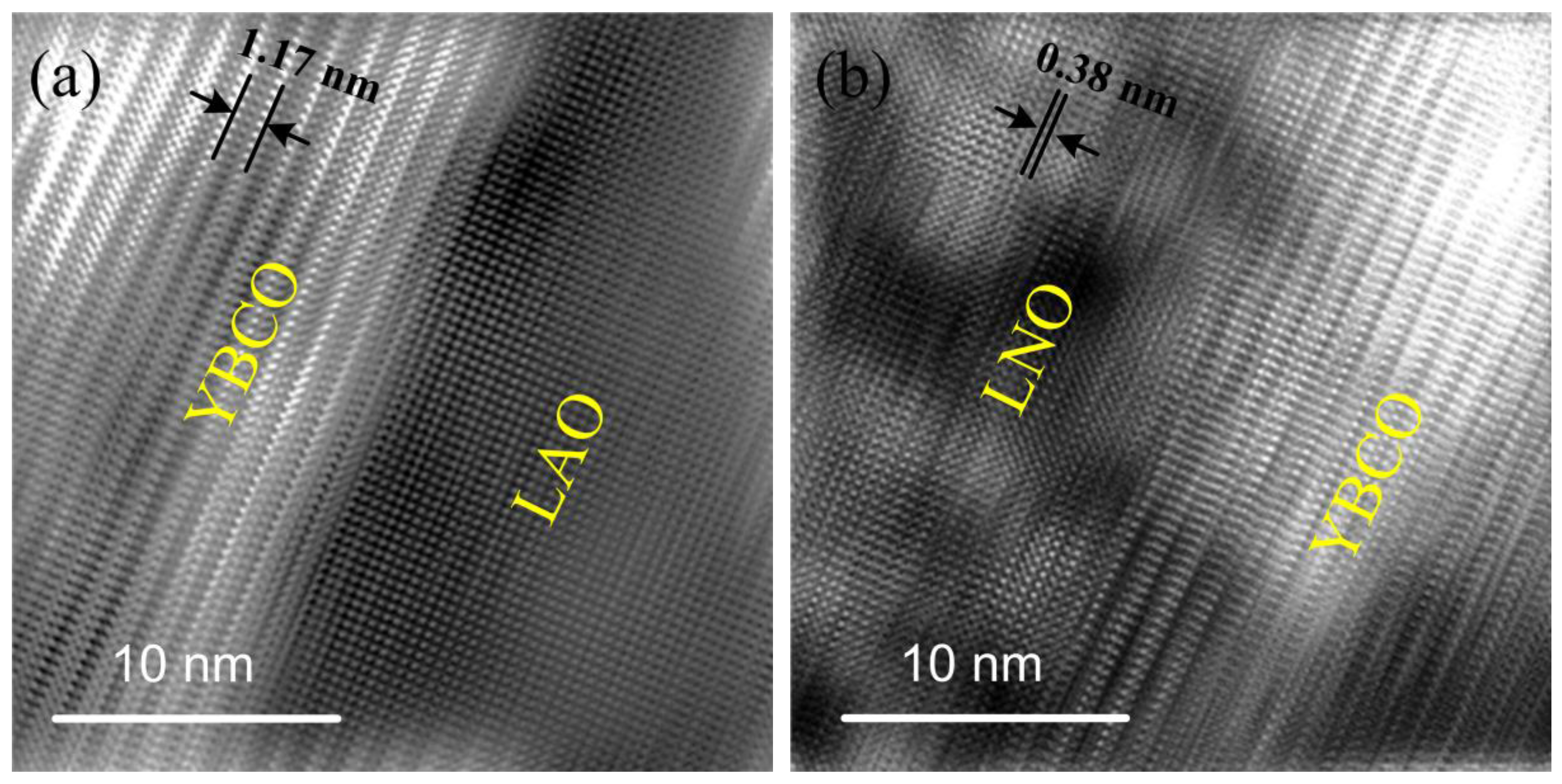
High-resolution TEM analysis is conducted for the marked square areas i and ii, and the acquired high-resolution TEM images (HRTEM) of the YBCO/LaAlO3 (LAO) and LaNiO3/YBCO (lower) interfaces are shown in Figure 3a,b. The interface between the LAO substrate and the YBCO film is clear, with atoms arranged in an orderly fashion. The inter-planar spacing of the YBCO film in the c-axis direction is 1.17 nm, which is similar to the lattice parameter of YBCO (c = 1.169 nm). The interface between the YBCO bottom film and the LaNiO3 middle film is relatively clear. The inter-planar spacing of the LaNiO3 film is 0.38 nm, which is similar to the lattice constant (a = 0.386 nm) of the LaNiO3 pseudocubic lattice.
To further analyse the atomic arrangement at the interfaces, a fast Fourier transform (FFT) was conducted and is shown in Figure 3c,d. In the FFT result of the YBCO/LAO interface, the diffraction points of YBCO(003) and LAO(001), YBCO(010) and LAO(010), and YBCO(013) and LAO(011) are coincident. Thus, the diffraction spots are intensified, indicating that the YBCO cells are cubic-on-cubic arranged on the LAO substrate. Likewise, in the LaNiO3/YBCO FFT result, the diffraction spots of YBCO(003) and LaNiO3(001), YBCO(010) and LaNiO3(010), and YBCO(013) and LaNiO3(011) are coincident. Accordingly, the diffraction spots are intensified, indicating that the LaNiO3 cells are cubic-on-cubic arranged on the YBCO. Consequently, LaNiO3 heteroepitaxial growth is realized on YBCO.
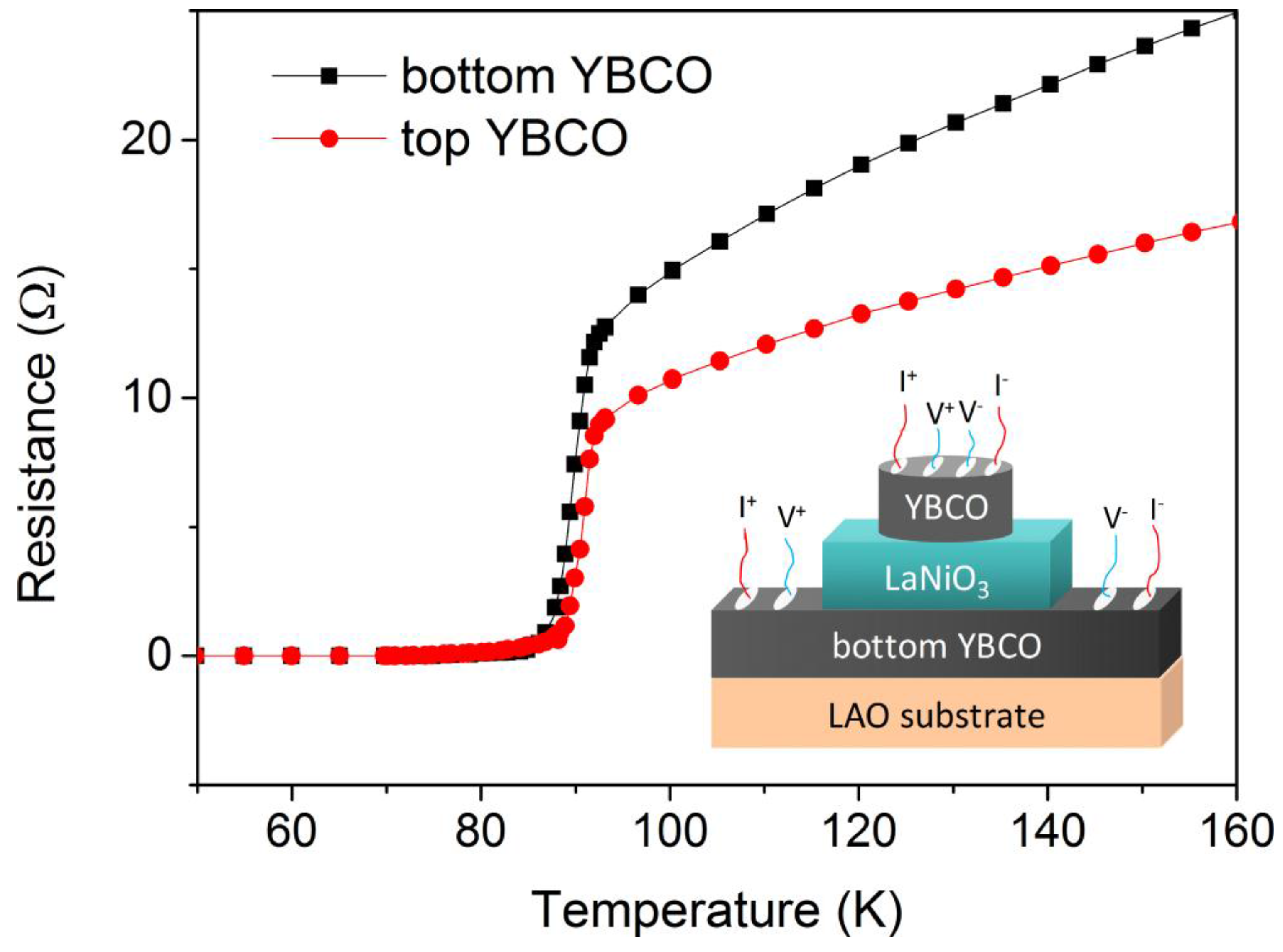
To further examine the superconductivity of the bottom and top YBCO films, R-T curves are acquired as shown in Figure 4. The resistances of the bottom and top YBCO films are reduced as the temperature is decreased. At approximately 90 K, the resistance decreases to zero, presenting typical superconducting transition characteristics. The superconducting transition temperature (Tc) of the bottom YBCO film is approximately 89 K, and the Tc of the top YBCO film is approximately 90 K, which further indicates that the deposited YBCO/LaNiO3/YBCO sandwich structure has favourable epitaxial growth characteristics.
4. Conclusions
The deposition of a YBa2Cu3O7−x/LaNiO3/YBa2Cu3O7−x sandwich structured film through a sol-gel method on a LaAlO3 (100) single-crystal substrate is studied in this paper. The biaxial texture characteristics of the deposited sandwich structure, the microstructure of the interface and the superconductivity of YBCO are further studied, reaching the following conclusions.
By reasonably controlling the heat treatment temperature of each layer (decreasing the heat treatment temperature layer-by-layer), YBa2Cu3O7−x/LaNiO3/YBa2Cu3O7−x sandwich structured films with epitaxial growth characteristics are deposited, so that the top and bottom YBCO films are superconducting.
The TEM result shows that the LaNiO3 cell growth on YBCO is in a cubic-on-cubic arrangement.
Acknowledgments
This project was supported by the National Natural Foundation of China (Nos. 51372198, 51672212), the Project of Science and Technology of Shaanxi Province (No. 2013KW14-01) and the Doctoral Innovation Foundation of Xi’an University of Technology (No. 310-11202j403).
Author Contributions
Gaoyang Zhao and Chuanbao Wu conceived and designed the experiments; Chuanbao Wu, Po Fang, Shasha Wang and Ye Zhang performed the experiments; Chuanbao Wu and Gaoyang Zhao analyzed the data; Chuanbao Wu wrote the paper.
Conflicts of Interest
The authors declare no conflict of interest.
References
- Bozovic, I.; Logvenov, G.; Verhoeven, M.A.J.; Caputo, P.; Goldobin, E.; Beasley, M.R. Giant Proximity Effect in Cuprate Superconductors. Phys. Rev. Lett. 2004, 93, 157002. [Google Scholar] [CrossRef] [PubMed]
- Kirzhner, T.; Koren, G. Pairing and the phase diagram of the normal coherence length ξN(T, x) above Tc of La2−xSrxCuO4 thin films probed by the Josephson effect. Sci. Rep. 2014, 4, 6244. [Google Scholar] [CrossRef] [PubMed]
- Char, K.; Colclough, M.S.; Geballe, T.H.; Myersa, K.E. High Tc superconductor-normal-superconductor Josephson junctions using CaRuO3 as the metallic barrier. Appl. Phys. Lett. 1993, 62, 196–198. [Google Scholar] [CrossRef]
- Chin, D.K.; Van Duzer, T. Novel all-high Tc epitaxial Josephson junction. Appl. Phys. Lett. 1991, 58, 753–755. [Google Scholar] [CrossRef]
- Hegde, M.S.; Satyalakshmi, K.M.; Mallya, R.M.; Rajeswari, M.; Zhang, H. Epitaxial LaNiO3 thin films: A normal metal barrier for SNS junction. J. Mater. Res. 1994, 9, 898–902. [Google Scholar] [CrossRef]
- Satyalakshmi, K.M.; Mallya, R.M.; Ramanathan, K.V.; Wu, X.D.; Brainard, B.; Gautier, D.C.; Vasanthacharya, N.Y.; Hegde, M.S. Epitaxial metallic LaNiO3 thin films grown by pulsed laser deposition. Appl. Phys. Lett. 1993, 62, 1233–1235. [Google Scholar] [CrossRef]
- Sagoi, M.; Kinno, T.; Yoshida, J.; Mizushima, K. Magnetic properties of LaNiO3 films and Josephson characteristics of Y1Ba2Cu3O7−y/LaNiO3/Au/Ag/Pb junctions. Appl. Phys. Lett. 1993, 62, 1833–1835. [Google Scholar] [CrossRef]
- Hegde, M.S.; Satyalakshmi, K.M.; Manoharan, S.S.; Kumar, D. Superconducting and non-superconducting oxide multilayers. Mater. Sci. Eng. B Adv. 1995, 32, 239–245. [Google Scholar] [CrossRef]
- Wu, W.; Feng, F.; Zhao, Y.; Tang, X.; Xue, Y.; Shi, K.; Huang, R.; Qu, T.; Wang, X.; Han, Z.; et al. A low-fluorine solution with a 2:1 F/Ba mole ratio for the fabrication of YBCO films. Supercond. Sci. Technol. 2014, 27, 055006. [Google Scholar] [CrossRef]
- Bhuiyan, M.S.; Paranthaman, M.; Salama, K. Solution-derived textured oxide thin films—A review. Supercond. Sci. Technol. 2006, 19, 049801. [Google Scholar] [CrossRef]
- Puig, T.; González, J.C.; Pomar, A.; Mestres, N.; Castaño, O.; Coll, M.; Gázquez, J.; Sandiumenge, F.; Piñol, S.; Obradors, X. The influence of growth conditions on the microstructure and critical currents of TFA-MOD YBa2Cu3O7 films. Supercond. Sci. Technol. 2005, 18, 1141–1150. [Google Scholar] [CrossRef]
- Chen, Y.Q.; Wu, C.B.; Zhao, G.Y.; You, C.Y. An advanced low-fluorine solution route for fabrication of high-performance YBCO superconducting films. Supercond. Sci. Technol. 2012, 25, 062001. [Google Scholar] [CrossRef]
- Chen, Y.Q.; Zhao, G.Y.; Gao, J.P. Photosensitive sol-gel preparation and micro-patterning of (100)-oriented (Ba0.7Sr0.3) TiO3 film on LaNiO3 electrode. J. Sol-Gel. Sci. Technol. 2011, 59, 164–168. [Google Scholar] [CrossRef]
- Wada, T.; Suzuki, N.; Ichinose, A.; Yaegashi, Y.; Yamauchi, H.; Tanaka, S. Phase stability and decomposition of superconductive YBa2Cu4O8. Appl. Phys. Lett. 1990, 57, 81–83. [Google Scholar] [CrossRef]
- Hammond, R.H.; Bormann, R. Correlation between the in situ growth conditions of YBCO thin films and the thermodynamic stability criteria. Physica C 1989, 162–164, 703–704. [Google Scholar] [CrossRef]
- Wu, C.B.; Zhao, G.Y.; Fang, P. Effect of the firing process on the critical current density of YBa2Cu3O7−x films derived from the sol-gel method. Mater. Chem. Phys. 2015, 167, 160–164. [Google Scholar] [CrossRef]
- Solovyov, V.F.; Wiesmann, H.J.; Suenaga, M. Nucleation of YBa2Cu3O7−x on buffered metallic substrates in thick precursor films made by the BaF2 process. Supercond. Sci. Technol. 2005, 18, 239–248. [Google Scholar] [CrossRef]
Figure 1.
θ–2θ, ω and ϕ scan patterns of YBCO/LaNiO3/YBCO sandwich strucutred films from different heat treatment temperatures. The corresponding tri-layer heat treatment temperatures of (a), (d) and (g) are 700/750/800 °C (top to bottom films), 725/750/800 °C (top to bottom films) and 740/750/800 °C (top to bottom films), respectively. (b), (e) and (h) are the corresponding ω scans, and (c), (f) and (i) are the corresponding ϕ scans. The YBCO (005) and YBCO (019) crystal planes are tested for ω and ϕ scans.
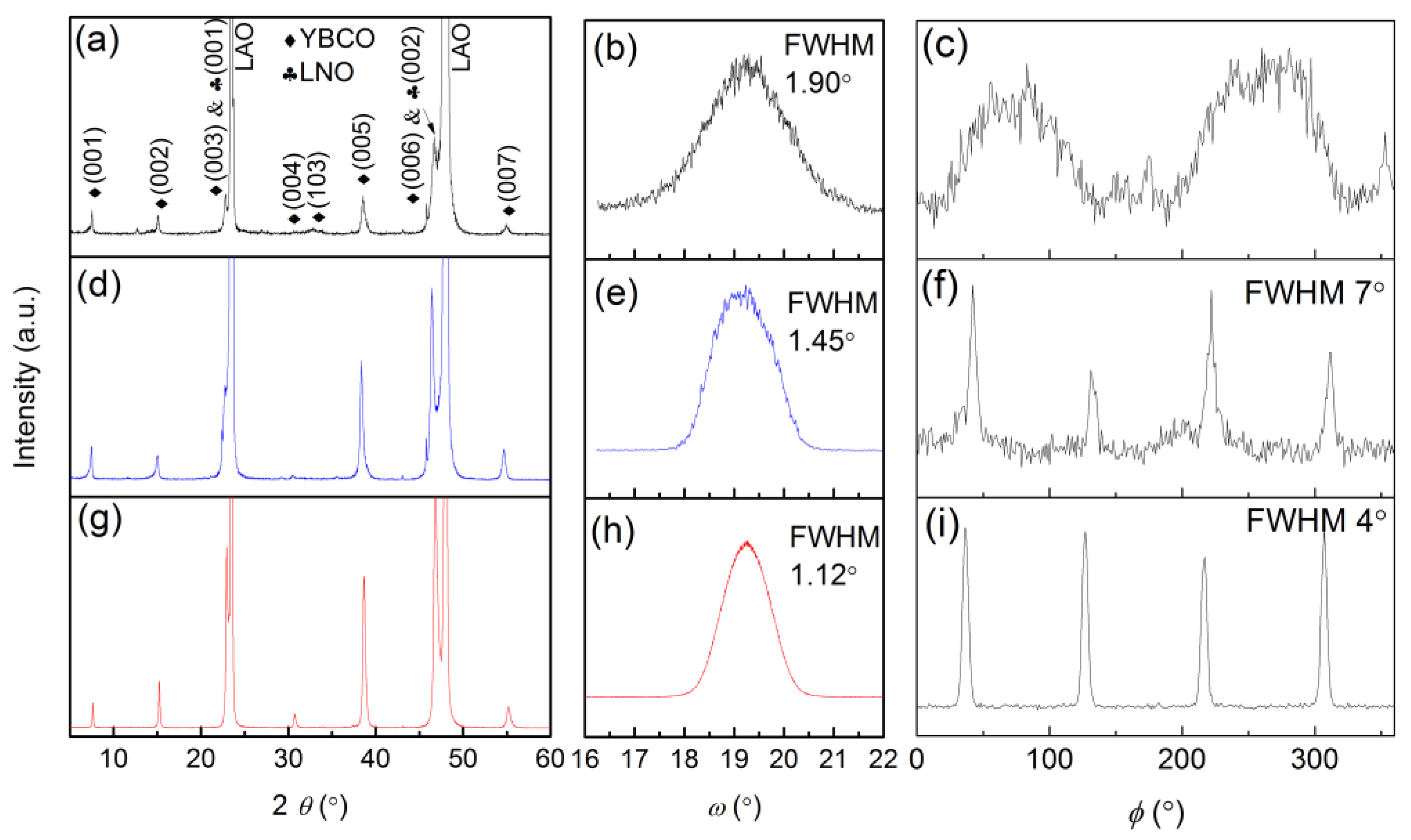
Figure 2.
TEM images of the YBCO/LaNiO3/YBCO sandwich structure.
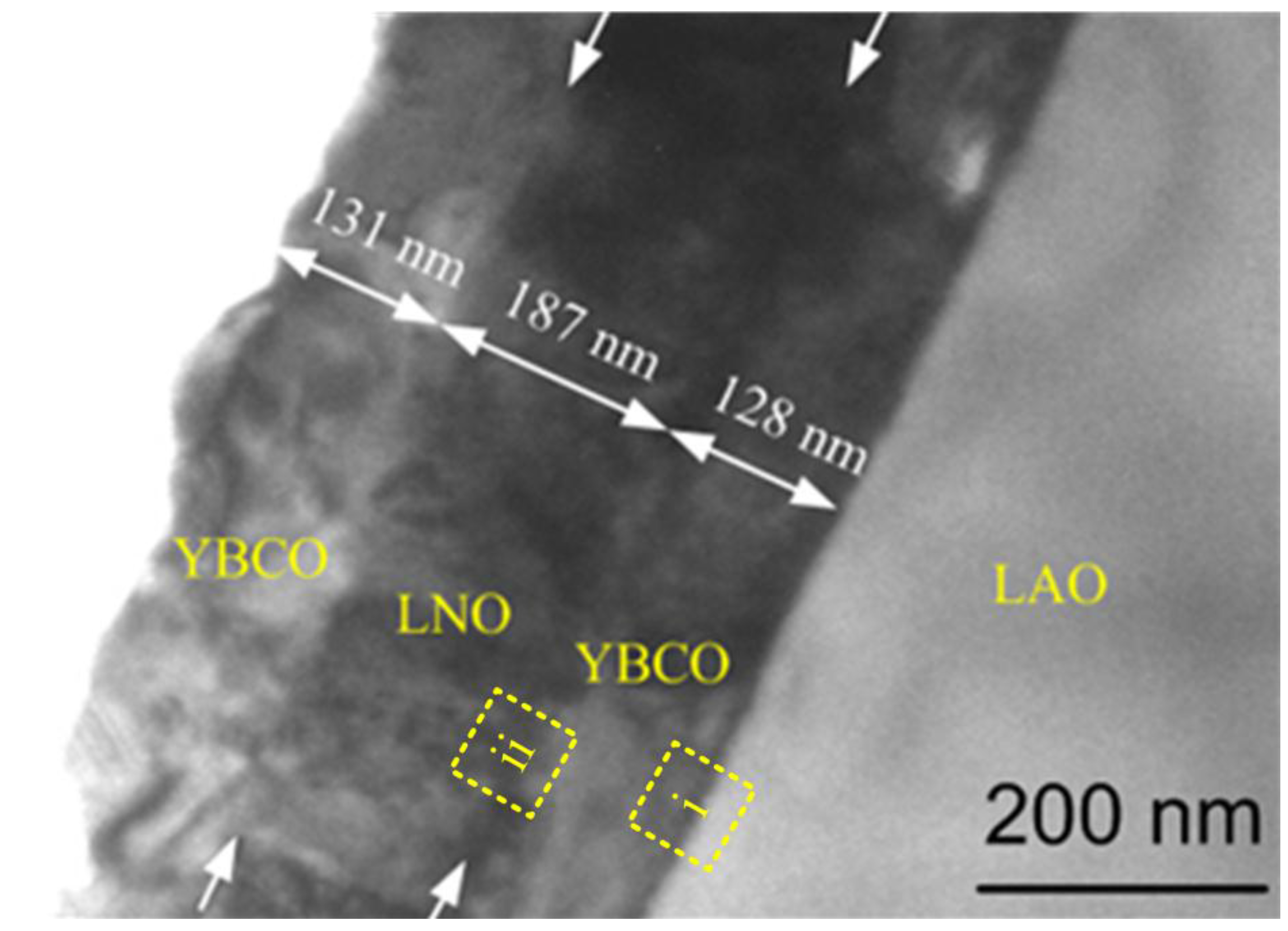
Figure 3.
HRTEM figures of the YBCO/LaNiO3/YBCO sandwich structure. (a) and (b) are the zoomed figures of square areas i and ii of Figure 2; (c) and (d) are the FFT figures of (a) and (b), respectively.
Figure 3.
HRTEM figures of the YBCO/LaNiO3/YBCO sandwich structure. (a) and (b) are the zoomed figures of square areas i and ii of Figure 2; (c) and (d) are the FFT figures of (a) and (b), respectively.

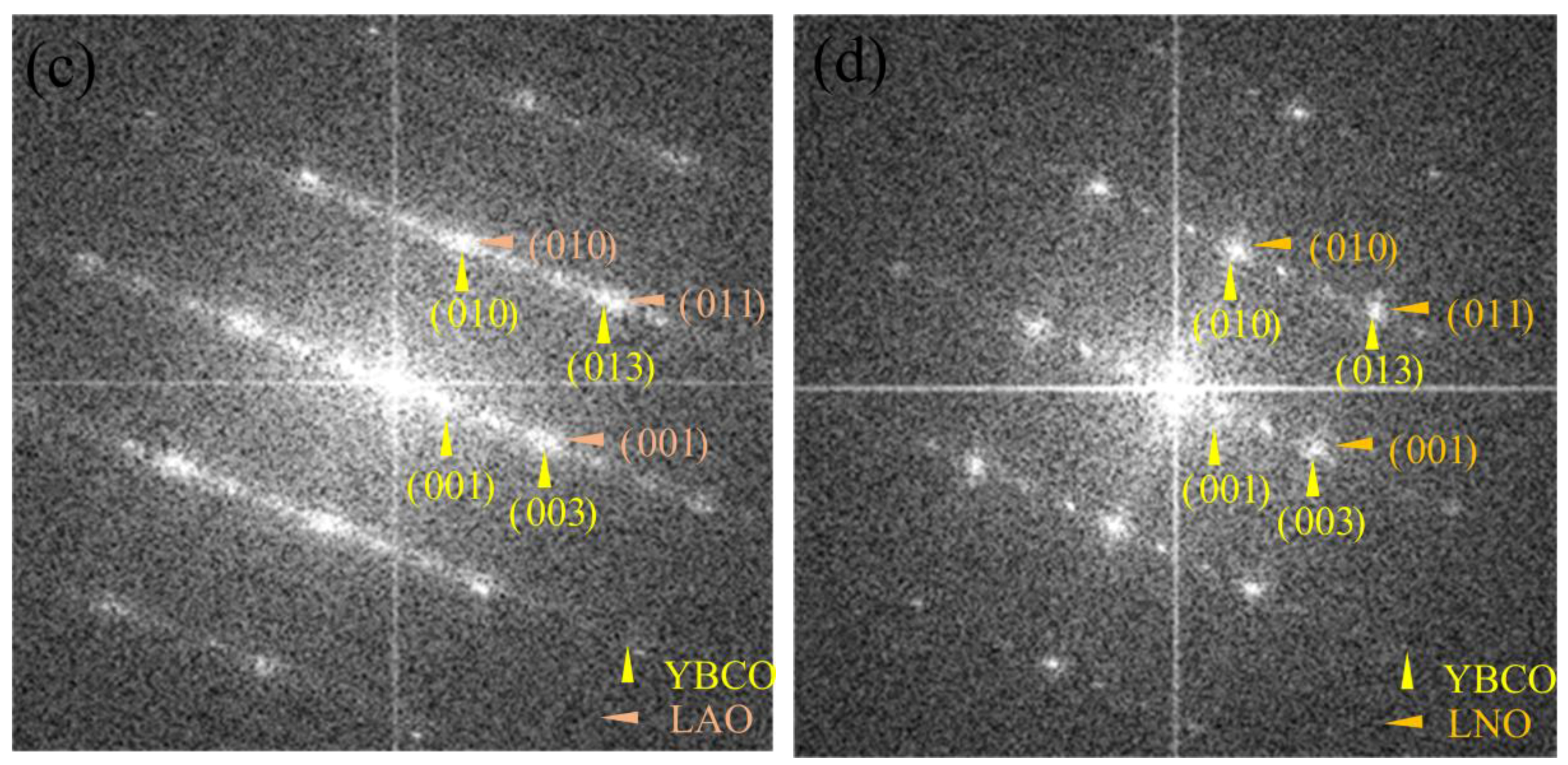
Figure 4.
R-T curves of the bottom and top YBCO layers of the YBCO/LaNiO3/YBCO sandwich structured films. The inset is a sketch map on R-T test for the top and bottom YBCO films in the tri-layer. A conductive silver paste was used to adhere the gold lead from the films to the sample stage.
Figure 4.
R-T curves of the bottom and top YBCO layers of the YBCO/LaNiO3/YBCO sandwich structured films. The inset is a sketch map on R-T test for the top and bottom YBCO films in the tri-layer. A conductive silver paste was used to adhere the gold lead from the films to the sample stage.

© 2017 by the authors. Licensee MDPI, Basel, Switzerland. This article is an open access article distributed under the terms and conditions of the Creative Commons Attribution (CC BY) license (http://creativecommons.org/licenses/by/4.0/).
Share and Cite
MDPI and ACS Style
Wu, C.; Zhao, G.; Fang, P.; Wang, S.; Zhang, Y. An All Sol-Gel Process for the Heteroepitaxial Growth of YBa2Cu3O7−x/LaNiO3/YBa2Cu3O7−x Tri-layer. Coatings 2017, 7, 62. https://doi.org/10.3390/coatings7050062
AMA Style
Wu C, Zhao G, Fang P, Wang S, Zhang Y. An All Sol-Gel Process for the Heteroepitaxial Growth of YBa2Cu3O7−x/LaNiO3/YBa2Cu3O7−x Tri-layer. Coatings. 2017; 7(5):62. https://doi.org/10.3390/coatings7050062
Chicago/Turabian StyleWu, Chuanbao, Gaoyang Zhao, Po Fang, Shasha Wang, and Ye Zhang. 2017. "An All Sol-Gel Process for the Heteroepitaxial Growth of YBa2Cu3O7−x/LaNiO3/YBa2Cu3O7−x Tri-layer" Coatings 7, no. 5: 62. https://doi.org/10.3390/coatings7050062
Note that from the first issue of 2016, this journal uses article numbers instead of page numbers. See further details here.