The Use of Triboemission Imaging and Charge Measurements to Study DLC Coating Failure

1
Tribology Group, Department of Mechanical Engineering, Imperial College London, London SW7 2AZ, UK
2
Institut P’, CNRS, Université de Poitiers, ISAE-ENSMA, F-86962 Futuroscope Chasseneuil, France
*
Authors to whom correspondence should be addressed.
Coatings 2017, 7(8), 129; https://doi.org/10.3390/coatings7080129
Submission received: 26 July 2017
/
Revised: 16 August 2017
/
Accepted: 17 August 2017
/
Published: 20 August 2017
(This article belongs to the Special Issue Manufacturing and Surface Engineering)
Abstract
:We present a study on the simultaneous evolution of the electron emission and surface charge accumulation that occurs during scratching tests in order to monitor coating failure. Steel discs coated with a diamond-like-carbon (DLC) film were scratched in both vacuum (~10−5 Torr) and atmospheric conditions, with electron emission and surface charge being measured by a system of microchannel plates and an electrometer, respectively. The results highlight a positive correlation between emission intensity values, surface charge measurements and surface damage topography, suggesting the effective use of these techniques to monitor coating wear in real time.

1. Introduction
Coatings are used extensively in many industrial and commercial applications in order to protect components that are subjected to sliding and rolling contact, both with and without liquid lubricants [1]. It has been shown that hard coatings and other surface modification methods are able to improve the resistance of rolling elements (i.e., bearings) to friction, wear and corrosion [2,3]. Thin diamond-like-carbon (DLC) coatings, for instance, provide protective, low friction, wear resistant surfaces for numerous industrial applications such as invasive and implantable medical devices, razor blades, magnetic hard discs and microelectromechanical systems [4,5,6,7,8,9,10]. However, because of mismatches in mechanical and electrical properties between the coating and substrate, residual stresses and chemical reactions can arise at the interface of the materials leading to the structural degradation of the coating. The evaluation of damage and the electrical state of the film/coating and substrate, along with the option to monitor the coatings failure are becoming important tools in the endeavour to extend the lifetime of widely used devices.
Recently, several techniques have been used to investigate coating failure. These include atomic force microscopy to map the evolution of cracks in nickel films on a polyimide substrate [11]; ultrasonic force microscopy to measure the debonding of glass films on polyethylene terephthalate substrate [12]; and scanning electron microscopes and thermographs to detect damage evolution [13,14]. In addition to these qualitative techniques, real-time in situ methods based on acoustic emission have been developed to obtain quantitative stress/strain information to study interfacial properties of coating/film systems [15,16].
In this paper, we propose a new in situ and real-time technique to monitor the failure of diamond-like-carbon coating on a steel substrate during sliding tests under vacuum and atmospheric conditions. The method combines triboemission imaging and tribocharging measurements. Triboemission refers to the emission of charged particles such as electrons, protons, positive ions and negative ions that occur during surface damage (i.e., cracking formation, wear) [17,18,19,20]—see the supplementary example video showing imaging of continuous electron emission arising from a moving alumina specimen scratched by a stationary diamond tip. These emissions correlate positively with the electrical resistivity of the rubbed material, which decreases from insulators to conductors (in the order: insulating > semi-conductive > conductive) [17,21]. Furthermore, our recent studies on the spatial characteristics of triboemission bursts have shown that their direction, shape, size and intensity depend on the failure mode of the materials (such as cracking and grain pull-out) [17,22]. Tribocharging measurements, on the other hand, are used to monitor the variation of the charge on the surface, which may be related to tribochemical reactions occurring at the surface contact area [23,24].
This work focuses on correlating the evolution of surface topography with the variation in emission intensity and the measured charge to demonstrate the applicability of electron emission and surface charge measurements as a means of studying coating failure. Finally, a comparison is made between charge measurements, obtained in vacuum and atmosphere, in order to show that such measurements are an effective means of detecting coating failure in practice.
2. Materials and Methods
Discs, made from 52100 steel, coated with a 1 μm layer of DLC (a-C: H sp3~50%, H~40%–characterisation provided by PCS Instruments, London, UK) were used as test specimens. These discs had a diameter of 46 mm and a thickness of 6 mm and were cleaned with toluene followed by isopropanol in an ultrasonic bath (15 min for each chemical), prior to each test.
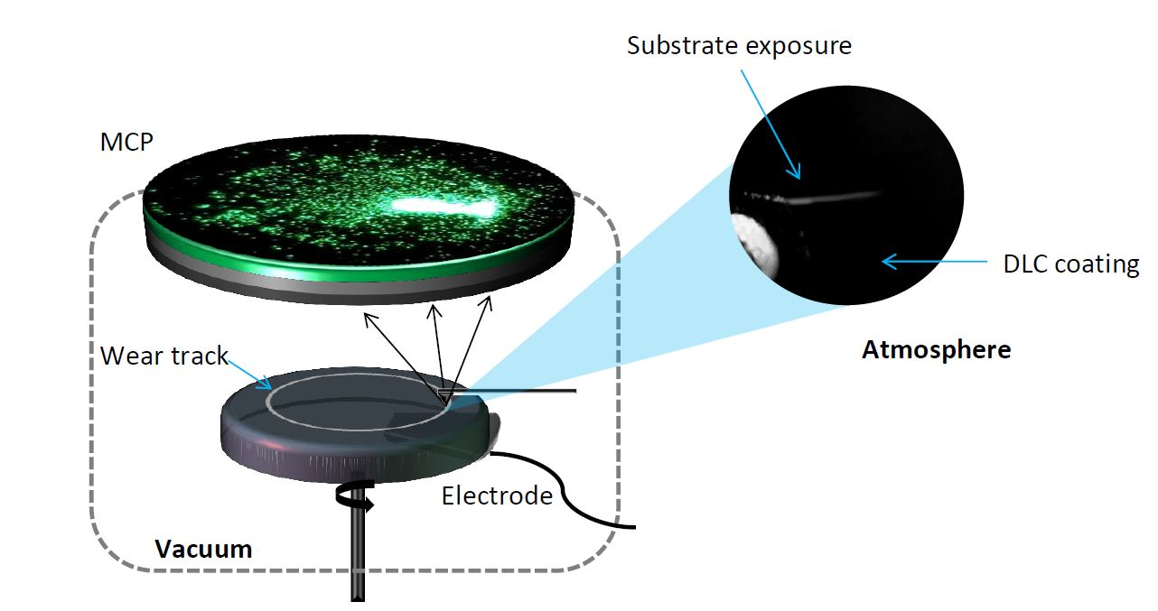
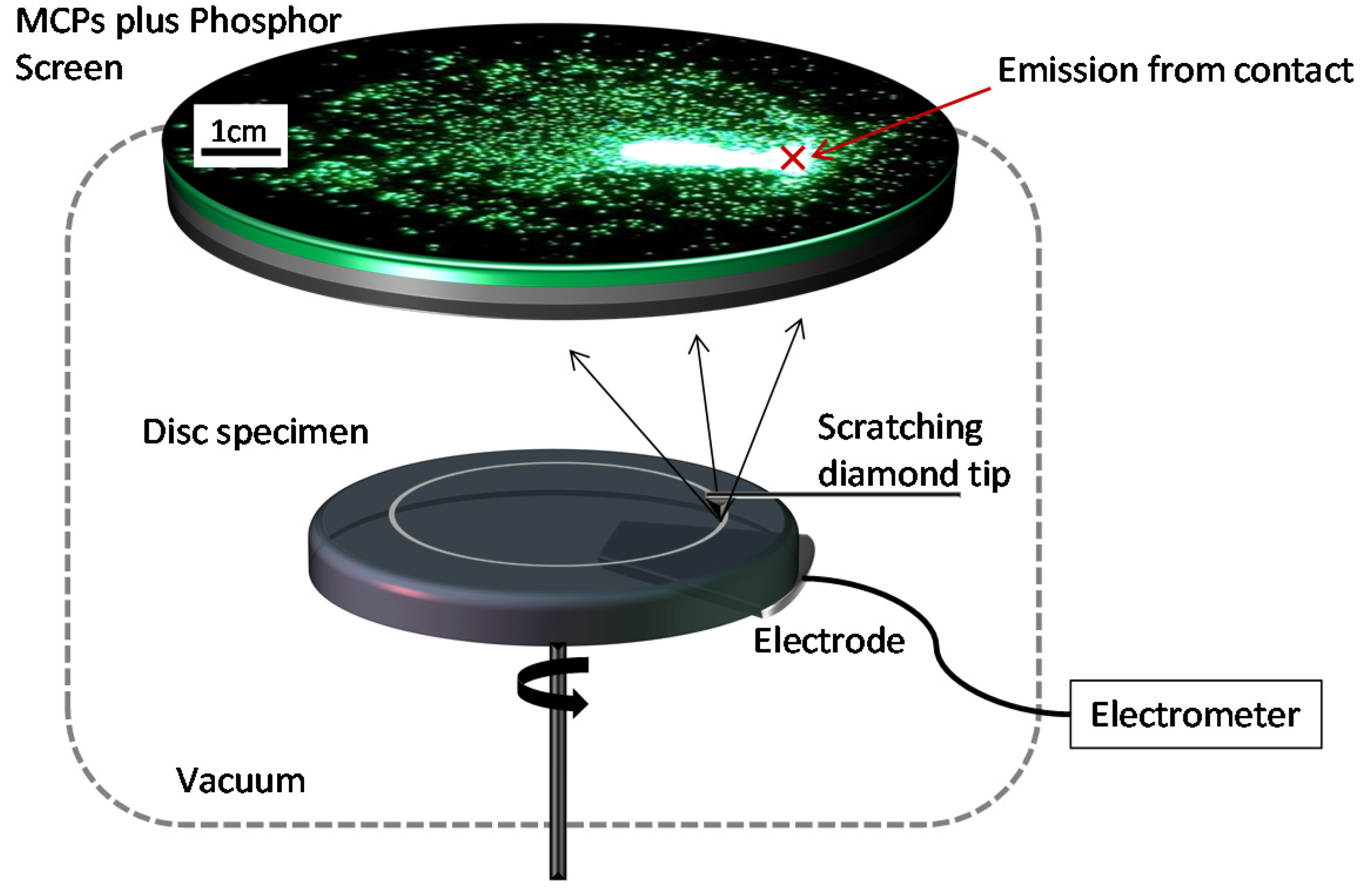
The tribometer used to conduct the study is represented schematically in Figure 1 [17,22]. It consists of a system of microchannel plates (MCPs, i.e., arrays of electrons multipliers), coupled with a phosphor screen (Photonis Inc., Sturbridge, MA, USA). The two circular MCPs, in a chevron arrangement with an active diameter of 75 mm, are located 10 mm above and parallel to the disc specimen (note: the centre of the circular MCPs are located directly above the centre of rotation of the disc). This setup allows us to obtain spatially resolved images of the triboemission, with 1:30 magnification due by the divergence of emitted electrons. The emissions detected and visualised through this system were recorded by a high speed camera (Phantom Miro eX, Vision Research Ltd., Bedford, UK) with a Fujian 35 mm f1.7 lens located above the experimental setup. The sliding contact was produced by loading a diamond tip of radius 100 μm (Synton-MDP Ltd., Port, Switzerland) against the rotating disc specimen. The rotation of the disc was recorded by the supplied PCS Instruments encoder device. In addition, an electrometer (Model: 6517b, Keithley Instruments Ltd., Bracknell, UK) coupled with a 10 mm × 5 mm metal sheet electrode attached underneath the specimen was used to inductively measure the charge of the surface, simultaneously with the emission detection. The tests were conducted in vacuum conditions at a pressure of ~10−5 Torr.
The triboemission measurements were conducted in negative particle detection mode, i.e., 10%–85% of 0.01–50 keV electrons were detected [25], with the voltage applied to the input MCP, output MCP and the phosphor screen being ground, applying 1.5 kV, and 5 kV, respectively. The speed of the rotation of the disc was 4 Hz giving a sliding velocity of 50 mm/s. The deadweight load applied to the scratching tip on to the disc was 0.5 N. The frame rate of the high-speed camera (exposure time 8 ms), the encoder and the electrometer acquisition were synchronised at 125 Hz. At the end of the test, the cleaning procedure previously described was repeated and the topography of the wear track was recorded using the Veeco Wyko NT9100 optical profiler (Veeco Instruments Inc., Plainview, NY, USA).
The failure of the coating in atmospheric conditions was assessed by focusing the high speed camera directly on the outlet of the contact. In this case, the MCPs and the phosphor screen system were replaced by the 5× magnification lenses.
3. Results and Discussion
3.1. Triboemission Measurements
The test apparatus used here differs significantly from those used in previous studies that measured the triboemission from hydrogenated carbon films in the vicinity of a sliding contact [26,27,28,29,30]. The spatial resolution achieved with this technique allows the emission to be visualised, defining its shape and size. This provides more detailed information than was previously obtained from single point measurements.
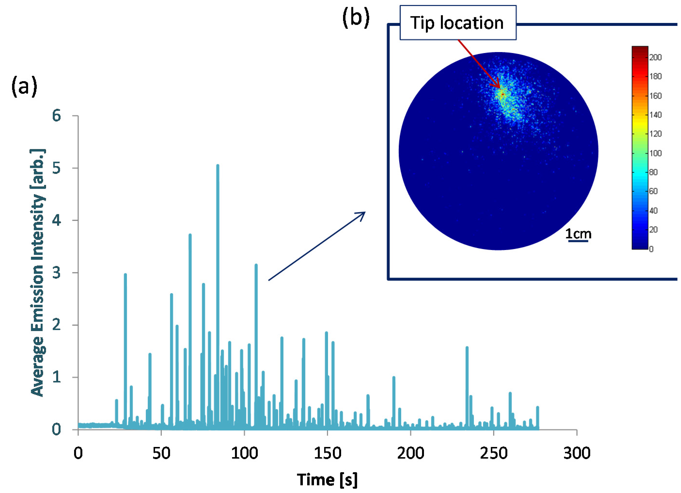
Figure 2a displays the average (spatial) intensity of each phosphor screen image plotted as a function of time, throughout the entire sliding test. In addition, Figure 2b shows an example of an emission event as viewed on the phosphor screen. The emission event is localised at the tip location suggesting that it is due to wear. In Figure 2a, a decrease in emission intensity is also evident during the second half of the test.
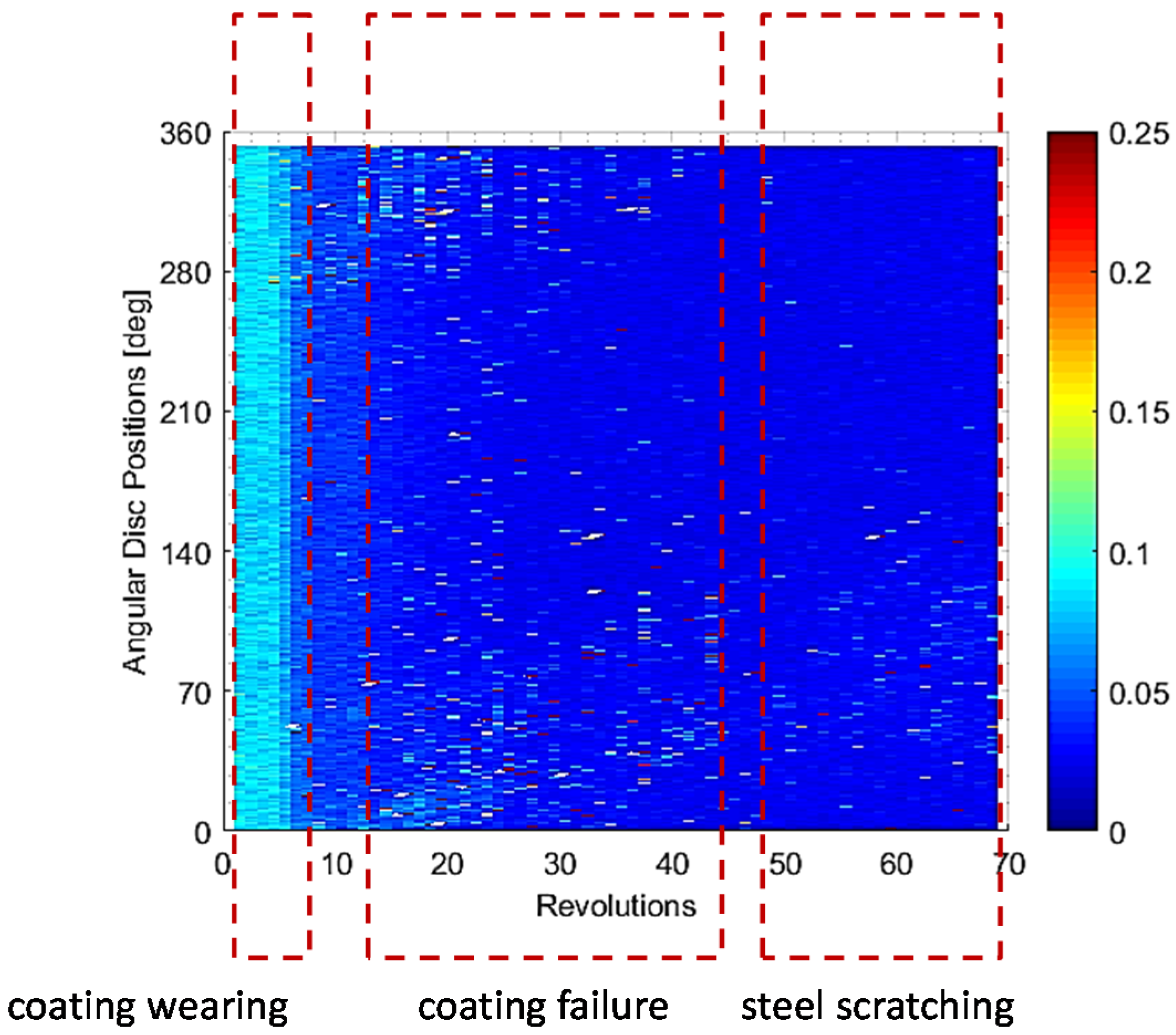
An alternative way to display the same phosphor screen intensity data is to plot the average emission intensity as a function of the cycles and the angular disc position of the stylus relative to the disc, as shown in Figure 3 (with each coloured square representing the average phosphor screen intensity). Here, the spatial evolution of the emissions can be visualised and divided into three regions. Initially, there is a moderate level of emission indicated by the pale blue rectangular section at the start of the test. Towards the end of this period, the first and highest intensity peak in emission occurs, and the low-level baseline emission transitions into the second stage of the test (shown by the background colour becoming dark blue). From this point onwards, sporadic high intensity peaks occur, although their intensity is lower than that of the first event. Eventually, the frequency and magnitude of these peaks reduce, as shown by the mostly uninterrupted dark blue region.
It is hypothesised that this observed behaviour is attributed to the following mechanism. The initial area characterised by a constant, low level intensity (the light blue colour) defines the emission generated by the wearing of the non-conductive coating layer as shown by the optical microscopy scan in Figure 4a. This is in accordance with previous studies on non-conductive materials [17]. The following high intensity emission event indicates the moment at which the coating fails resulting in a wear trace characterised by both surface cracks and partial delamination (Figure 4b). This is in accordance with previous studies that suggest that emission is due to the high energy generated during the damage of the surface, in particular crack formation [17,19,31,32]. The third region shows relatively few high emission events, occurring due to wearing of the remaining coating. The baseline emission (shown by the dark blue colour) is at a low level due to the scratching of the metal substrate, which can conduct away charge and hence prevents emission. This is in agreement with the fact that the triboemission intensity is greater for materials with high electrical resistivity [33].
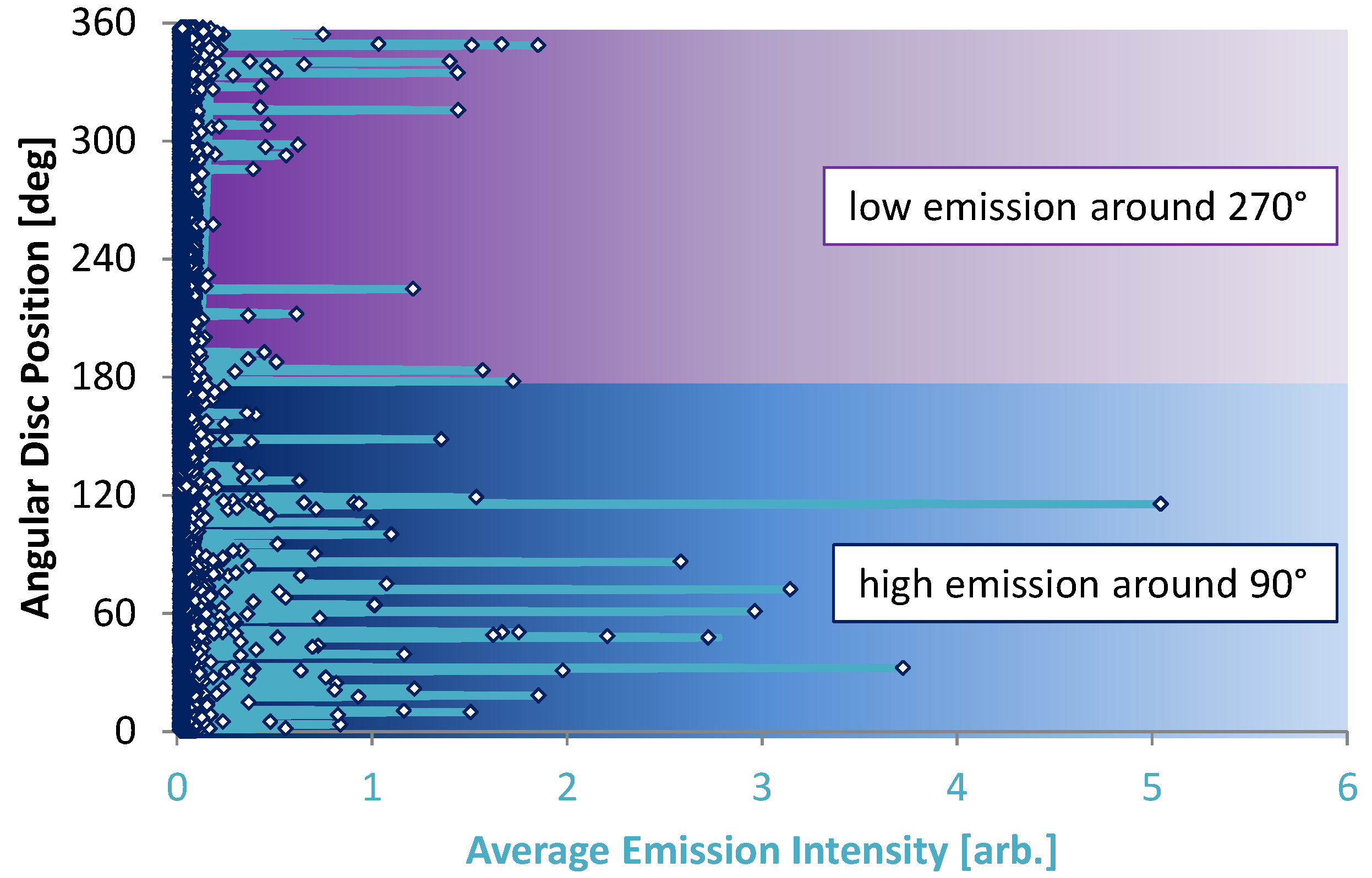
Since the angular position of the disc is recorded and synchronised with the camera acquisition, the average emission intensity can be plotted as a function of the angular position of the disc as shown in Figure 5. Here, it is evident that the highest intensity emissions are localised around 90° and the lowest intensity emission are around 270° of disc rotation. Visual inspection of the disc revealed that the depth of wear around the track was not uniform. It was therefore hypothesized that the area of the disc characterised by high intensity emission events corresponded to the diamond tip contacting the non-conductive coating. Conversely, the area characterised by low emission events corresponded with the tip scratching the conductive steel.
After the test, a Veeco optical profilometer analysis of the surface was conducted to evaluate the depth of the wear track in the two areas under consideration. Results are shown in Figure 6. It can be seen that the wear track at the angular position of 270° is 1.69 μm, which is deeper than the thickness of the coating layer (Figure 6b). In the region of the disc surface around the 90° location, the depth is only 0.1042 μm, which is less than the thickness of the coating layer, as shown in Figure 6d. This proves that, around the 90° location, the coating was not removed so that the tip scratched the coating generating an emission in accordance with triboemission measurements for non-conductive materials. However, around 270°, the tip scratched the metal substrate and the intensity of the emission was reduced in accordance with previous emission measurements for conductive materials.
These results clearly show the possibility of using this technique to monitor the coating failure in real time by evaluating the evolution of the emission events and by identifying the area of the failure. There is an issue however, which is that the microchannel plate measurements must be carried out within a vacuum. For this reason, the following charge measurements were performed.
3.2. Charge Measurements
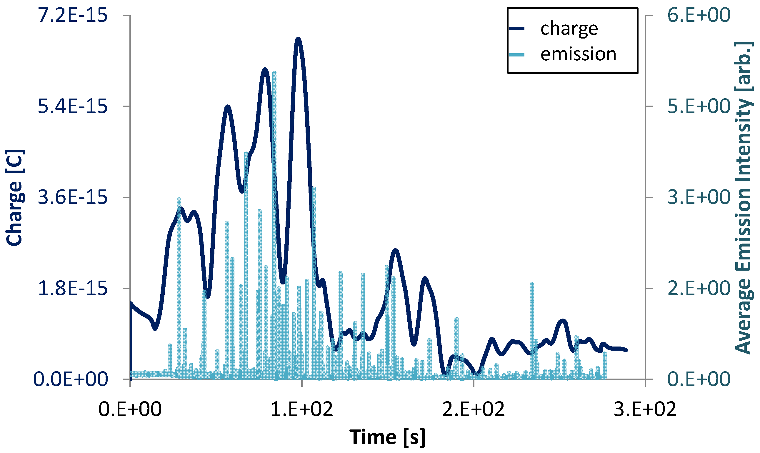
The release of the emission was then compared with the evolution of the charge on the disc surface. To do this, instantaneous measurements of charge on the surface and the average of the emission intensity are plotted as a function of time in Figure 7. There is a clear correspondence between the emission intensity and the charge accumulation for the DLC surface (a local regression smoothing method was applied to the charge measurement data for a better comparison). In the first part of the test, there is a clear correspondence between the negative emission peaks and the positive charge peaks. This suggests that the surface charges positively, at least partly due to electrons leaving the surface. At around 100 s, the reduction of the emission intensity and the charge can be attributed to the failure of the coating. It is suggested that this reduction is caused by: (i) the scratching of a reduced area of coating (part of the coating is removed during the first 100 s of the test); (ii) the exposure of the metal substrate which switches the contact from being diamond/DLC to being diamond/steel, preventing the accumulation of opposite charge on each of the two counter bodies which would otherwise lead to emission; and (iii) the exposure of the steel substrate which may absorb charge, preventing the generation of emission.
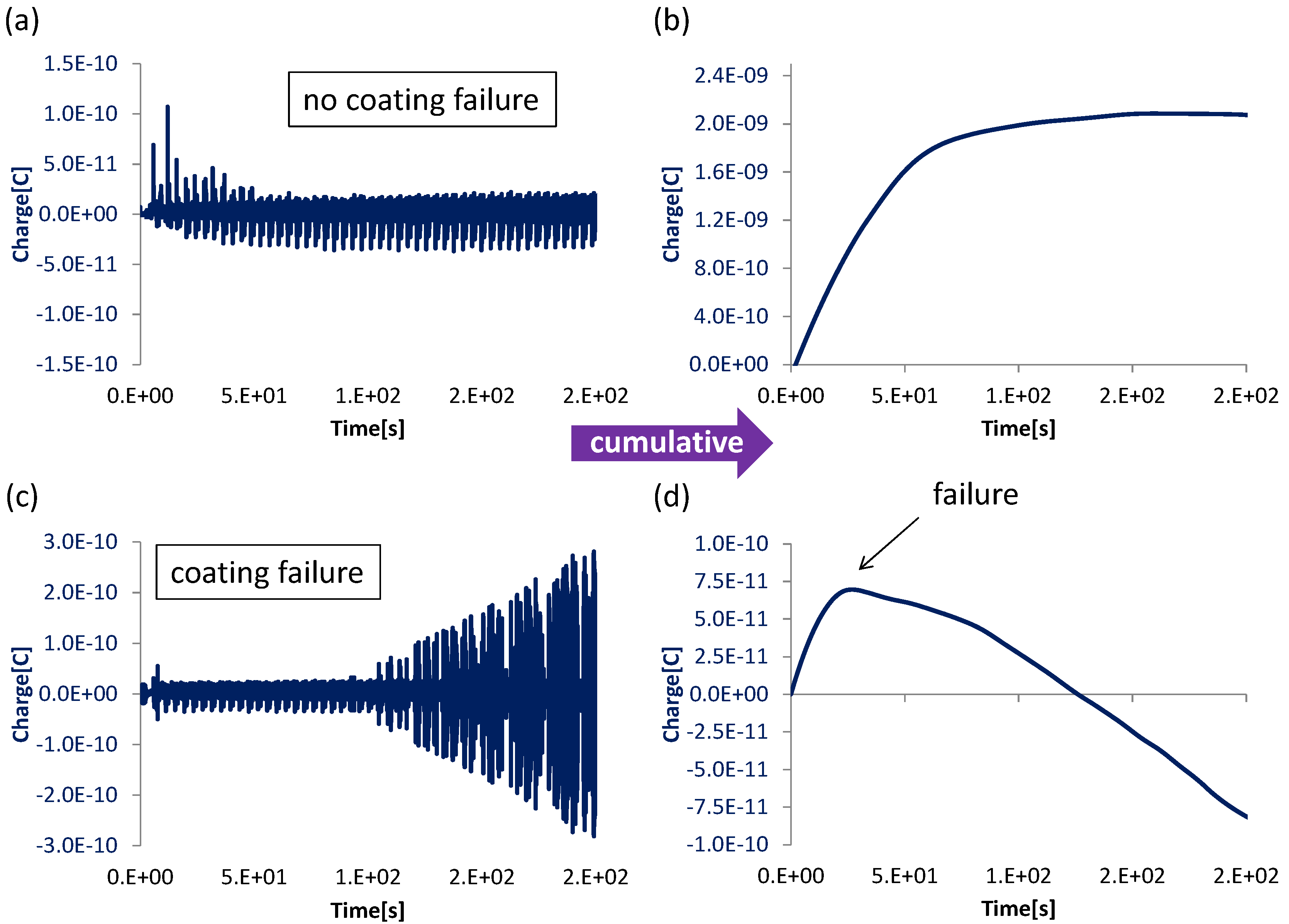
Additional measurements were assessed to compare the differences in charging behaviour between tests in which coating failure either did or did not occur (Figure 8). The curves of instantaneous charge values show a fluctuation for both no failure and failure tests—see Figure 8a,c, respectively. Figure 8a shows that, in the case of no coating failure, the charge fluctuates around 10 pC for the entire test. However, the cumulative values in Figure 8b show positive charges accumulating on the surface, as also reported by previous studies [34], until a saturation value is reached, from which point onwards the charging remains stable. In the case of coating failure, the instantaneous charge curve fluctuates around 10 pC until the point failure, after which it increases, as shown in Figure 8c. The cumulative curve in Figure 8d shows that, after failure, the surface started to accumulate negative charge. This is suggested to be caused by the reasons outlined above.
This comparison clearly shows the differing charging behaviours in the case of failure and no failure of the coating. The accumulation on the surface of positive particles due to the emission of negative particles is affected in the case of failure.
3.3. Measurements under Atmosphere
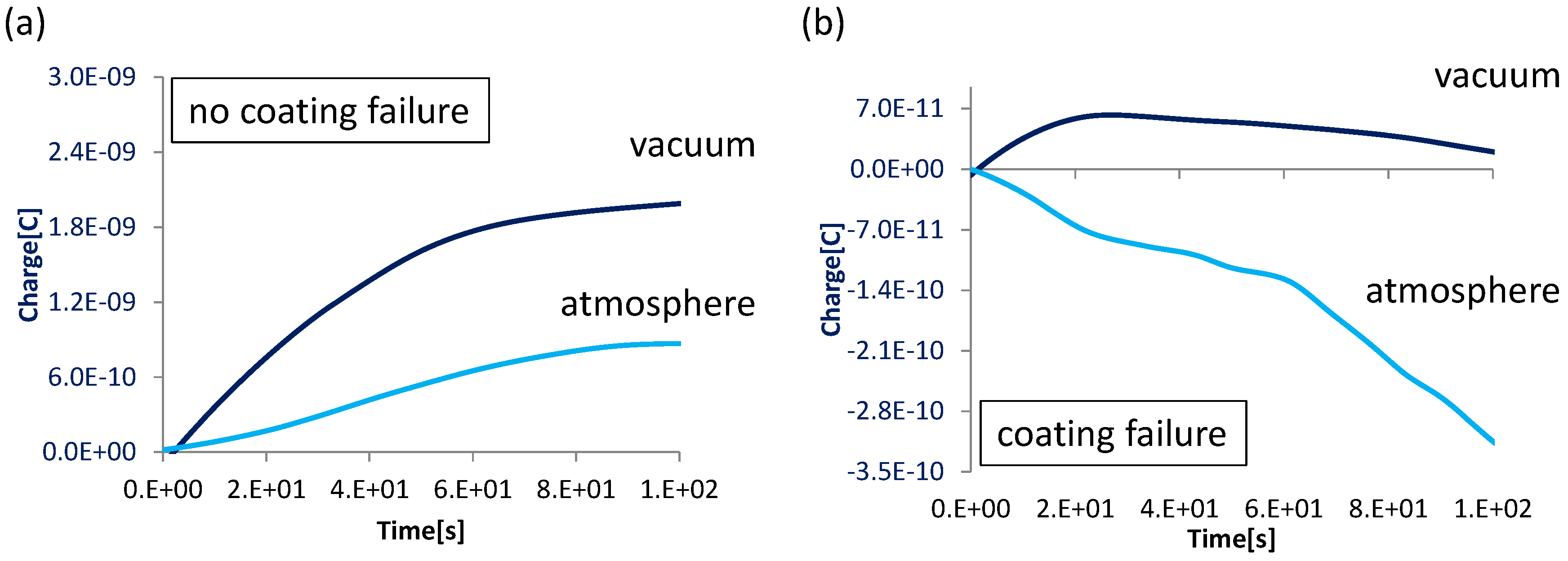
The final investigation was aimed at comparing the charging of the surface in both vacuum and atmospheric conditions. A comparison for the charge measurements when failure did and did not occur is reported in Figure 9. When the coating remains intact, the surface charges positively in both vacuum and atmospheric conditions, as shown in Figure 9a. In the case of failure, the surface charges negatively as soon as the metal substrate is exposed, as reported in Figure 9b. In each case, the value of the charge in the atmosphere is lower compared to that under vacuum conditions. This may be due to increased electrical breakdown due to the presence of air. Specifically, when the electric field due to the accumulation of charge on components exceeds a threshold determined by the dielectric field strength [35] of the surrounding gas (30 kV/cm for air [36]), breakdown can occur through a Townsend discharge process. Furthermore, some evidence suggests that corona discharge limits the formation of charge during contact electrification [37,38].
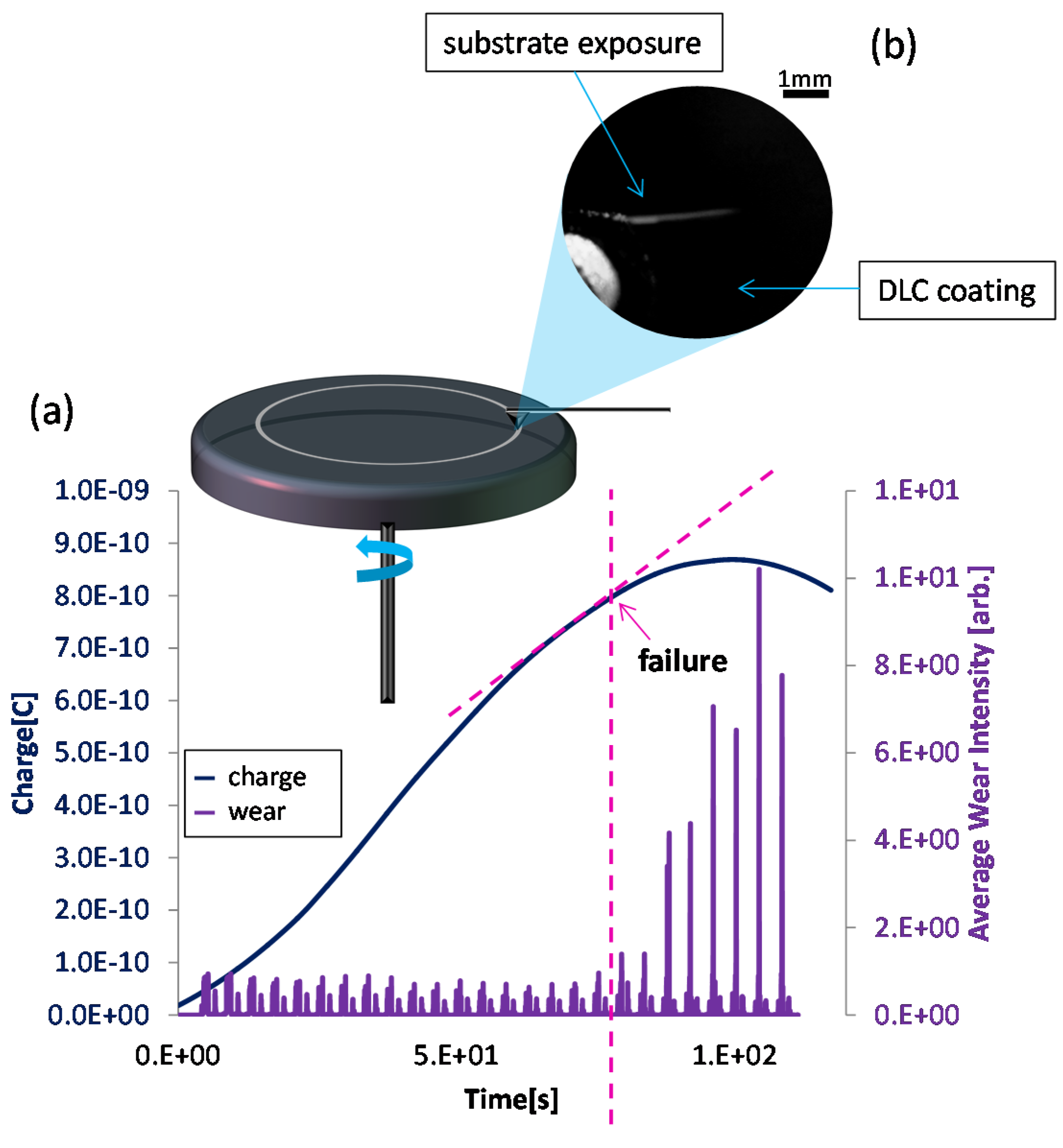
The charge measurements in atmosphere were accompanied by standard optical microscope video recordings of the wear track. This gave an in situ indication of the instantaneous coating integrity on the specimen surface during sliding, by acquiring and averaging the colour intensity of pixels recorded at the exit of the contact. The increase in the intensity indicates the exposure of the metal substrate, since steel has a higher reflectivity compared to DLC coating. The average of the intensity at the exit of the contact and the measured surface charge are plotted against time in Figure 10a. This plot shows that, when the tip wears the coating without failure, the surface charges positively. However, as soon as the coating fails (the moment of the failure is indicated by the dashed line) the metal substrate is exposed, as show in Figure 10b, and the surface charge begins to decrease towards negative values in accordance with previous results.
4. Conclusions
The present paper reports the potential of measuring charged particle emission and/or tribocharging for studying or monitoring the failure of coatings. The spatial information of triboemission allows us to identify the exact time and location of the failure. The evolution of the failure during the sliding and the change in the characteristic of the contact can also be monitored. The phosphor screen images show that the onset of coating failure is accompanied by high intensity emission events, while the exposure of the metal substrate is shown to cause a decrease in background emission intensity. This is attributed to the conductive substrate preventing the build-up of charge. The comparison between the emission and the charging of the surface again shows that triboemission is linked to accumulation of the charge on the surface. Specifically, the peaks of emission and peaks of positive charge coincide, showing that the surface charge is influenced by the negative particle emission leaving the contact.
In atmosphere, the trends in the charge measurements are comparable with those carried out in vacuum, but their magnitudes are consistently lower. The surface charges positively during sliding contact until failure occurs, after which, it charges negatively. It is suggested that the values measured in atmosphere are lower than in vacuum either due to the oxidation reactions which passivate the active fresh material or because the presence of air leads to dielectric breakdown. The charge measurements are supported by qualitative measurements of surface reflectivity. Here, the appearance of the conductive metal substrate is followed by a change from positive to negative surface charge. Overall, these results suggest that charge and emission measurements may be effective in monitoring the failure of coatings in real time and their ability to provide more detailed information will be assessed in future work.
Supplementary Materials
The supplementary video, Video S1: Electron emission from alumina specimen, is available online at https://www.mdpi.com/2079-6412/7/8/129/s1.
Acknowledgments
This research was supported by the UK Engineering and Physical Research Sciences Research Council, with equipment funding provided by the Taiho Kogyo Tribology Research Foundation.
Author Contributions
A.C. and T.R. conceived and designed the experiments; A.C. performed the experiments and analyzed the data; J.L.R. contributed for the design of the test rig; A.C. wrote the paper.
Conflicts of Interest
The authors declare no conflict of interest.
References
- Holmberg, K.; Mathews, A. Coatings tribology: a concept, critical aspects and future directions. Thin Solid Films 1994, 253, 173–178. [Google Scholar] [CrossRef]
- Stewart, S.; Ahmed, R. Rolling contact fatigue of surface coatings—A review. Wear 2002, 253, 1132–1144. [Google Scholar] [CrossRef]
- Maurer, R. Friction, wear, and corrosion control in rolling bearings through coatings and surface modification: A review. J. Vac. Sci. Technol. A 1986, 4, 3002–3006. [Google Scholar] [CrossRef]
- Raveh, A.; Martinu, L.; Gujrathi, S.C.; Klemberg-Sapieha, J.E.; Wertheimer, M.R. Structure-property relationships in dual-frequency plasma deposited hard aC: H films. Surf. Coat. Technol. 1992, 53, 275–282. [Google Scholar] [CrossRef]
- Raveh, A.; Martinu, L.; Hawthorne, H.M.; Wertheimer, M.R. Mechanical and tribological properties of dual-frequency plasma-deposited diamond-like carbon. Surf. Coat. Technol. 1993, 58, 45–55. [Google Scholar] [CrossRef]
- Martinu, L. Hard carbon films deposited under high ion flux. Thin Solid Films 1992, 208, 42–47. [Google Scholar] [CrossRef]
- Butter, R.; Allen, M.; Chandra, L.; Lettington, A.H.; Rushton, N. In vitro studies of DLC coatings with silicon intermediate layer. Diam. Relat. Mater. 1995, 4, 857–861. [Google Scholar] [CrossRef]
- Snyders, R.; Bousser, E.; Amireault, P.; Klemberg-Sapieha, J.E.; Park, E.; Taylor, K.; Casey, K.; Martinu, L. Tribo-Mechanical Properties of DLC Coatings Deposited on Nitrided Biomedical Stainless Steel. Plasma Process. Polym. 2007, 4, S640–S646. [Google Scholar] [CrossRef]
- Grill, A. Tribology of diamondlike carbon and related materials: An updated review. Surf. Coat. Technol. 1997, 94, 507–513. [Google Scholar] [CrossRef]
- Grill, A. Diamond-like carbon: state of the art. Diam. Relat. Mater. 1999, 8, 428–434. [Google Scholar] [CrossRef]
- George, M.; Coupeau, C.; Colin, J.; Grilhé, J. Atomic force microscopy observations of successive damaging mechanisms of thin films on substrates under tensile stress. Thin Solid Films 2003, 429, 267–272. [Google Scholar] [CrossRef]
- McGuigan, A.P.; Huey, B.D.; Briggs, G.A.D.; Kolosov, O.V.; Tsukahara, Y.; Yanaka, M. Measurement of debonding in cracked nanocomposite films by ultrasonic force microscopy. Appl. Phys. Lett. 2002, 80, 1180–1182. [Google Scholar] [CrossRef]
- Qian, L.; Zhu, S.; Kagawa, Y.; Kubo, T. Tensile damage evolution behavior in plasma-sprayed thermal barrier coating system. Surf. Coat. Technol. 2003, 173, 178–184. [Google Scholar] [CrossRef]
- Busso, E.P.; Wright, L.; Evans, H.E.; McCartney, L.N.; Saunders, S.R.J.; Osgerby, S.; Nunn, J. A physics-based life prediction methodology for thermal barrier coating systems. Acta Mater. 2007, 55, 1491–1503. [Google Scholar] [CrossRef] [Green Version]
- Lu, P.; Chou, Y.K.; Thompson, R.G. Short-time Fourier Transform Method in AE Signal Analysis for Diamond Coating Failure Monitoring in Machining Applications. In Proceedings of the ASME 2010 International Manufacturing Science and Engineering Conference, Erie, PA, USA, 12–15 October 2010; Volume 1. [Google Scholar]
- Mao, W.G.; Wu, D.J.; Yao, W.B.; Zhou, M.; Lu, C. Multiscale monitoring of interface failure of brittle coating/ductile substrate systems: A non-destructive evaluation method combined digital image correlation with acoustic emission. J. Appl. Phys. 2011, 110, 084903. [Google Scholar] [CrossRef]
- Ciniero, A.; Le Rouzic, J.; Baikie, I.; Reddyhoff, T. The Origins of Triboemission—Correlating Electron Emission with Surface Damage. Wear 2017, 374–375, 113–119. [Google Scholar] [CrossRef]
- Dickinson, J.; Donaldson, E.; Park, M. The emission of electrons and positive ions from fracture of materials. J. Mater. Sci. 1981, 16, 2897–2908. [Google Scholar] [CrossRef]
- Nakayama, K.; Suzuki, N.; Hashimoto, H. Triboemission of charged particles and photons from solid surfaces during frictional damage. J. Phys. D Appl. Phys. 1992, 25, 303–308. [Google Scholar] [CrossRef]
- Molina, G.J.; Furey, M.J.; Ritter, A.L.; Kajdas, C. Triboemission from alumina, single crystal sapphire, and aluminum. Wear 2001, 249, 214–219. [Google Scholar] [CrossRef]
- Nakayama, K.; Hashimoto, H. Triboemission from various materials in atmosphere. Wear 1991, 147, 335–343. [Google Scholar] [CrossRef]
- Le Rouzic, J.; Reddyhoff, T. Spatially Resolved Triboemission Measurements. Tribol. Lett. 2014, 55, 245–252. [Google Scholar] [CrossRef]
- Nakayama, K.; Nevshupa, R.A. Plasma generation in a gap around a sliding contact. J. Phys. D Appl. Phys. 2002, 35, L53–L56. [Google Scholar] [CrossRef]
- Nakayama, K.; Nevshupa, R.A. Effect of dry air pressure on characteristics and patterns of tribomicroplasma. Vacuum 2004, 74, 11–17. [Google Scholar] [CrossRef]
- Wiza, J.L. Microchannel plate detectors. Nucl. Instrum. Methods 1979, 162, 587–601. [Google Scholar] [CrossRef]
- Matta, C.; Eryilmaz, O.L.; De Barros Bouchet, M.I.; Erdemir, A.; Martin, J.M.; Nakayama, K. On the possible role of triboplasma in friction and wear of diamond-like carbon films in hydrogen-containing environments. J. Phys. D Appl. Phys. 2009, 42, 075307. [Google Scholar] [CrossRef]
- Nakayama, K.; Yamanaka, K.; Ikeda, H.; Sato, T. Friction, wear, and triboelectron emission of hydrogenated amorphous carbon films. Tribol. Trans. 1997, 40, 507–513. [Google Scholar] [CrossRef]
- Nakayama, K.; Ikeda, H. Triboemission characteristics of electrons during wear of amorphous carbon and hydrogenated amorphous carbon films in a dry air atmosphere. Wear 1996, 198, 71–76. [Google Scholar] [CrossRef]
- Nakayama, K. Triboemission of electrons, ions, and photons from diamondlike carbon films and generation of tribomicroplasma. Surf. Coat. Technol. 2004, 188–189, 599–604. [Google Scholar] [CrossRef]
- Nakayama, K.; Bou-Said, B.; Ikeda, H. Tribo-Electromagnetic Phenomena of Hydrogenated Carbon Films—Tribo-Electrons, -Ions, -Photons, and -Charging. J. Tribol. 1997, 119, 764–768. [Google Scholar] [CrossRef]
- Dickinson, J.T. Fracto-emission: The role of charge separation. J. Vac. Sci. Technol. A 1984, 2, 1112–1116. [Google Scholar] [CrossRef]
- Walton, A.J. Triboluminescence. Adv. Phys. 2006, 26, 887–948. [Google Scholar] [CrossRef]
- Nakayama, K. Tribocharging and friction in insulators in ambient air. Wear 1996, 194, 185–189. [Google Scholar] [CrossRef]
- Kornfeld, M. Frictional electrification. J. Phys. D Appl. Phys. 1976, 9, 1183–1192. [Google Scholar] [CrossRef]
- Vella, S.J.; Chen, X.; Thomas, S.W., III; Zhao, X.; Suo, Z.; Whitesides, G.M. The determination of the location of contact Electrification-induced discharge Events. J. Phys. Chem. C 2010, 114, 20885–20895. [Google Scholar] [CrossRef] [Green Version]
- Lide, D.R.; Haynes, W.M.; Bruno, T.J. CRC Handbook of Chemistry and Physics, 9th ed.; CRC Press: Boca Raton, FL, USA, 2015. [Google Scholar]
- Fabian, A.; Krauss, C.; Sickafoose, A.; Horanyi, M.; Robertson, S. Measurements of electrical discharges in Martian regolith simulant. IEEE Trans. Plasma Sci. 2001, 29, 288–291. [Google Scholar] [CrossRef]
- Thomas, S.W.; Vella, S.J.; Kaufman, G.K.; Whitesides, G.M. Patterns of electrostatic charge and discharge in contact electrification. Angew. Chem. 2008, 120, 6756–6758. [Google Scholar] [CrossRef]
Figure 1.
Schematic of the tribometer.

Figure 2.
(a) Average Emission Intensity (spatial average of each phosphor screen image) vs. time, (complete test); (b) Phosphor screen intensity of a single emission event.
Figure 2.
(a) Average Emission Intensity (spatial average of each phosphor screen image) vs. time, (complete test); (b) Phosphor screen intensity of a single emission event.

Figure 3.
Average phosphor screen intensity as a function of time and disc position.

Figure 4.
Optical Microscopy scans of the wear trace during (a) coating wearing phase; (b) coating failure phase.
Figure 4.
Optical Microscopy scans of the wear trace during (a) coating wearing phase; (b) coating failure phase.
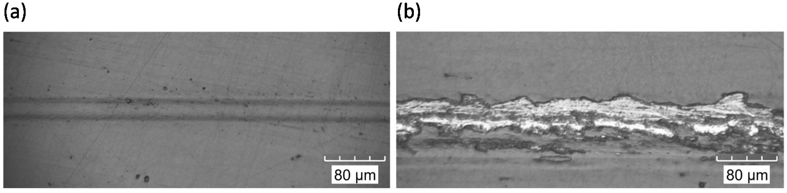
Figure 5.
Average of phosphor screen intensity as a function of emission intensity and disc position.
Figure 5.
Average of phosphor screen intensity as a function of emission intensity and disc position.

Figure 6.
Veeco analysis of the surface at disc regions of low and high emission, (a) 3D profile at 270°; (b) section depth at 270°; (c) 3D profile at 90°; (d) section depth at 90°.
Figure 6.
Veeco analysis of the surface at disc regions of low and high emission, (a) 3D profile at 270°; (b) section depth at 270°; (c) 3D profile at 90°; (d) section depth at 90°.
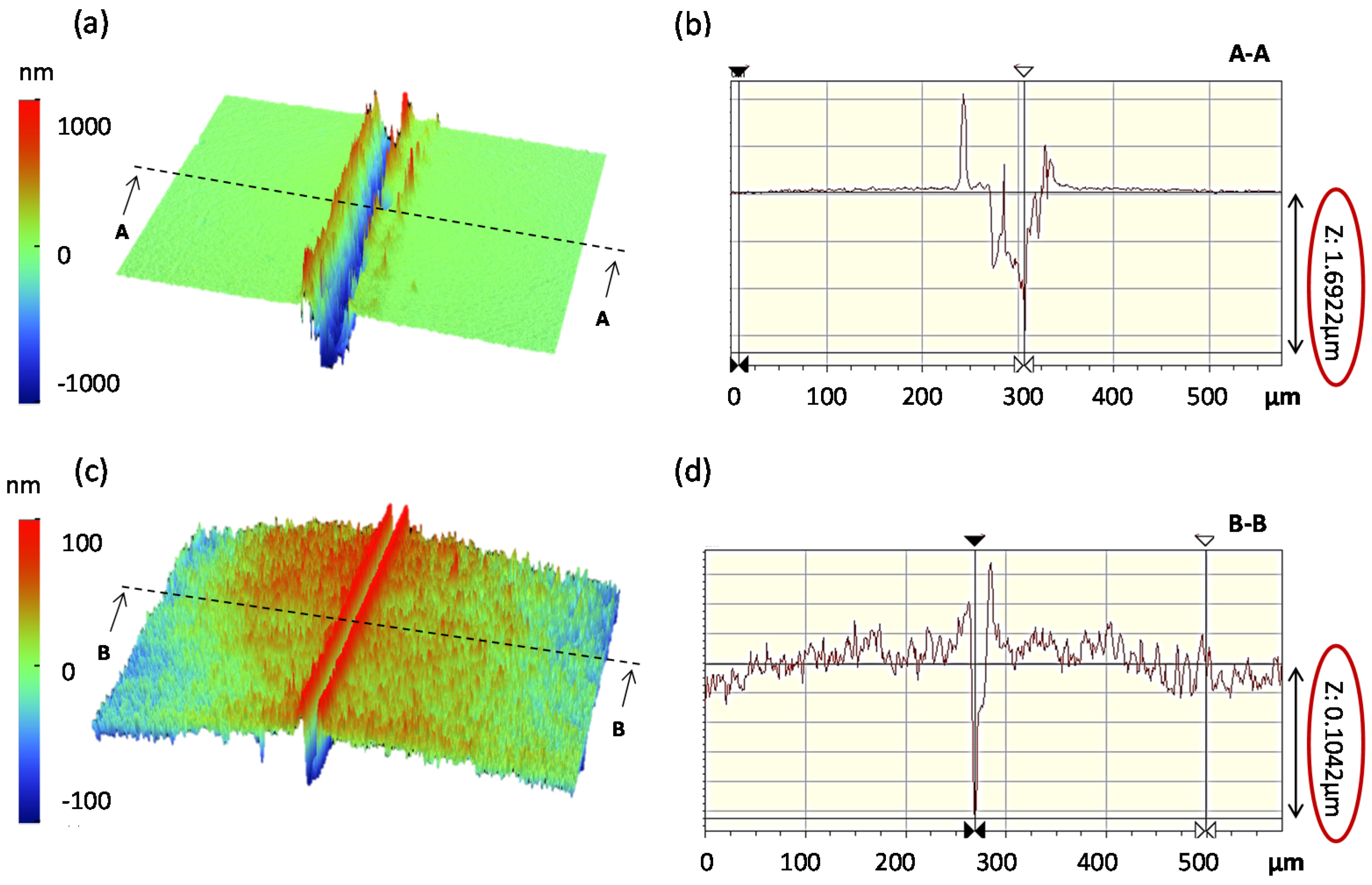
Figure 7.
Instantaneous values of average phosphor screen intensity and surface charge vs. time.

Figure 8.
Surface charge vs. time: (a) no coating failure—instantaneous; (b) no coating failure—cumulative; (c) coating failure—instantaneous; (d) coating failure—cumulative.
Figure 8.
Surface charge vs. time: (a) no coating failure—instantaneous; (b) no coating failure—cumulative; (c) coating failure—instantaneous; (d) coating failure—cumulative.

Figure 9.
Surface charge vs time in vacuum and atmosphere: (a) no coating failure—cumulative; (b) coating failure—cumulative.
Figure 9.
Surface charge vs time in vacuum and atmosphere: (a) no coating failure—cumulative; (b) coating failure—cumulative.

Figure 10.
(a) Average wear track intensity and surface charge vs. time; (b) example of 5× magnification wear track tip outlet.
Figure 10.
(a) Average wear track intensity and surface charge vs. time; (b) example of 5× magnification wear track tip outlet.
© 2017 by the authors. Licensee MDPI, Basel, Switzerland. This article is an open access article distributed under the terms and conditions of the Creative Commons Attribution (CC BY) license (http://creativecommons.org/licenses/by/4.0/).
Share and Cite
MDPI and ACS Style
Ciniero, A.; Le Rouzic, J.; Reddyhoff, T. The Use of Triboemission Imaging and Charge Measurements to Study DLC Coating Failure. Coatings 2017, 7, 129. https://doi.org/10.3390/coatings7080129
AMA Style
Ciniero A, Le Rouzic J, Reddyhoff T. The Use of Triboemission Imaging and Charge Measurements to Study DLC Coating Failure. Coatings. 2017; 7(8):129. https://doi.org/10.3390/coatings7080129
Chicago/Turabian StyleCiniero, Alessandra, Julian Le Rouzic, and Tom Reddyhoff. 2017. "The Use of Triboemission Imaging and Charge Measurements to Study DLC Coating Failure" Coatings 7, no. 8: 129. https://doi.org/10.3390/coatings7080129
Note that from the first issue of 2016, this journal uses article numbers instead of page numbers. See further details here.