Design of Nano-Porous Multilayer Antireflective Coatings


1
Department of Electrical and Computing Engineering, University of Toronto, Toronto ON M5S 3G4, Canada
2
Materials Science and Engineering Department, University of Toronto, Toronto ON M5S P3E4, Canada
*
Author to whom correspondence should be addressed.
Coatings 2017, 7(9), 134; https://doi.org/10.3390/coatings7090134
Submission received: 29 July 2017
/
Revised: 18 August 2017
/
Accepted: 24 August 2017
/
Published: 26 August 2017
(This article belongs to the Special Issue Antireflective Coatings for Glass and Transparent Polymers)
Abstract
:We present an overview of the design potential of nano-porous anti-reflection coatings (ARCs) and the associated challenges in its fabrication. Genetic algorithm optimization for the most effective ARCs on glass for normal and all incident angles is carried out and an admittance loci-based pictorial is used to visualize their performance. We then describe the advantages of using nano-porous multi-layers vis-à-vis other types of moth-eye type nano-grating films: Principally trading high performance and high cost of fabrication for good performance and lower cost facile synthesis. We describe some of the issues involved in the fabrication of such multi-layer stacks on glass and polymeric substrates and provide suggestions for overcoming these limitations.
1. Introduction
The technology of optical coatings has advanced significantly since the time of Joseph von Fraunhofer (1787–1826) who, in the process of etching glass surfaces, observed a reduction of its reflectivity. Along with Augustin-Jean Fresnel’s (1788–1827) formulation of the reflectance caused by an optical interface, and Lord Rayleigh’s (1842–1919) investigations into the interference effects of a multilayer stack, the field of anti-reflective coatings (ARCs) has developed tremendously to encompass a wide variety of designs suitable for most any optical application [1]. The discovery of nano-conical structures that envelope the moth’s eye has initiated a new direction into a new type of anti-reflective surface comprising a periodic grating surface of nano-structures that are carefully shaped to provide a gradual change in refractive index toward the ambient index [2,3,4].
However, the field of multi-layer structures has also undergone a renaissance with the ability to layer nano-thick films in a cost efficient and scalable manner. The designs of such multi-layer structures are constrained by the material’s index of refraction which typically ranges from 1.5 to 3.0, thus necessitating elaborate designs of many layers with different types of materials in order to produce the optimal interference effects. However, it is possible to relax the material constraints by introducing a degree of porosity f into the material packing, through which its effective refractive index then follows a simple equation . By relaxing this fundamental constraint, it would then be possible to optimize the ARC design to only a few layers, bringing down costs and yet opening up the design space. Already, it is trivial to produce a single layer coating comprising of a dip coated 10 nm silica nanoparticle film, that by virtue of its inherent minimum 26% to 32% porosity through close packing of spheres in a Hexagonally-Closed Packed or Body-Closed Packed arrangement, reduces the reflectivity of a PMMA (Poly(methyl methacrylate)) substrate significantly (Figure 1).
In this article, the question that we investigate is that, given the relaxed constraints of being able to relatively easily tune the refractive index of a nano-thick layer, how can one determine an optimized ARC stack that is anti-reflective even at glancing angle incidence and is relatively broadband in the visible. The solution will serve as a guide in designing the ARC stack for various applications. Here, we turn to using an established method called Admittance Loci representation to aid in understanding the solutions proposed by Genetic Algorithm optimization [5,6]. The challenges of fabricating and maintaining such a stack and their suggested solutions will also be discussed.
2. Materials and Methods
We first provide a brief summary of the Genetic Algorithm used to optimize the transmittance of 2 types of four-layer stacks for normal incidence (0°) and angular incidence (0 to 80°) on a single optical interface of a semi-infinite substrate with the refractive index of glass. A semi-infinite substrate was chosen as it can be easily represented by an admittance locus representation. 3D binary arrays representing the individuals and optical parameters were generated randomly within pre-defined constraints (1.0 < n < 1.54 and 45 nm < z < 120 nm). The optical parameters were fed into the Abeles transmittance matrix to produce a transmittivity curve and a corresponding normalized fitness value Rave which is defined as
where λmin and λmax represent the spectral range of interest, and RTE(λ) and RTM(λ) are the TE (Transverse Electric) and TM (Transverse Magnetic) mode spectral reflectivities. After evaluating a series of multi-layer systems and thus creating a population of fitness values, the systems were selected for breeding via a proportionate selection process, where the normalized fitness value of each system would have a proportionately finite probability of being selected. The fitter individual system has a high chance of pairing with another fit individual system. The parent systems are replicated as their children, where crossover between the parent systems’ chromosomes has a high chance of occurring. Finally, random mutations of 1% are introduced for diversity and to decrease the chance of missing a global optimal solution. After this application of selection, crossover and mutation, a new generation of optical parameters are fed into the Abeles matrix to generate another population of fitness values. It is found that convergence to the highest fit is achieved in 23 generations while the algorithm was run for a total of 100 generations.
As an instructive guide, the admittance loci for the TE mode where the performance is optimized for normal incidence and for angular incidence using a four-layer ARC is presented in the next section (with corresponding TM mode admittance loci presented in the appendix). An admittance locus, which is confined to the right-hand side of the complex plane, is a geometric representation of the performance of multilayer stack at a specific value of wavelength. It comprises a continuous series of circular arcs representing each layer of the multilayer stack with its starting point (admittance of the substrate) on the real axis. The optical thickness of each layer is represented by its degree of arc in the clockwise direction. A typical multilayer ARC stack will thus trace out a helicoid path. For example, a semicircle corresponds to a quarter wave optically thick layer, a full circle corresponding to a half wave layer. The radius of circle is described by the Equation (2):
where n is the index of the substrate, Yj is the admittance at the j-th layer. The point (1,0) on the complex plane denotes zero reflectance, and the greater the distance the loci end-point is from (1,0) the greater the reflectance will be.
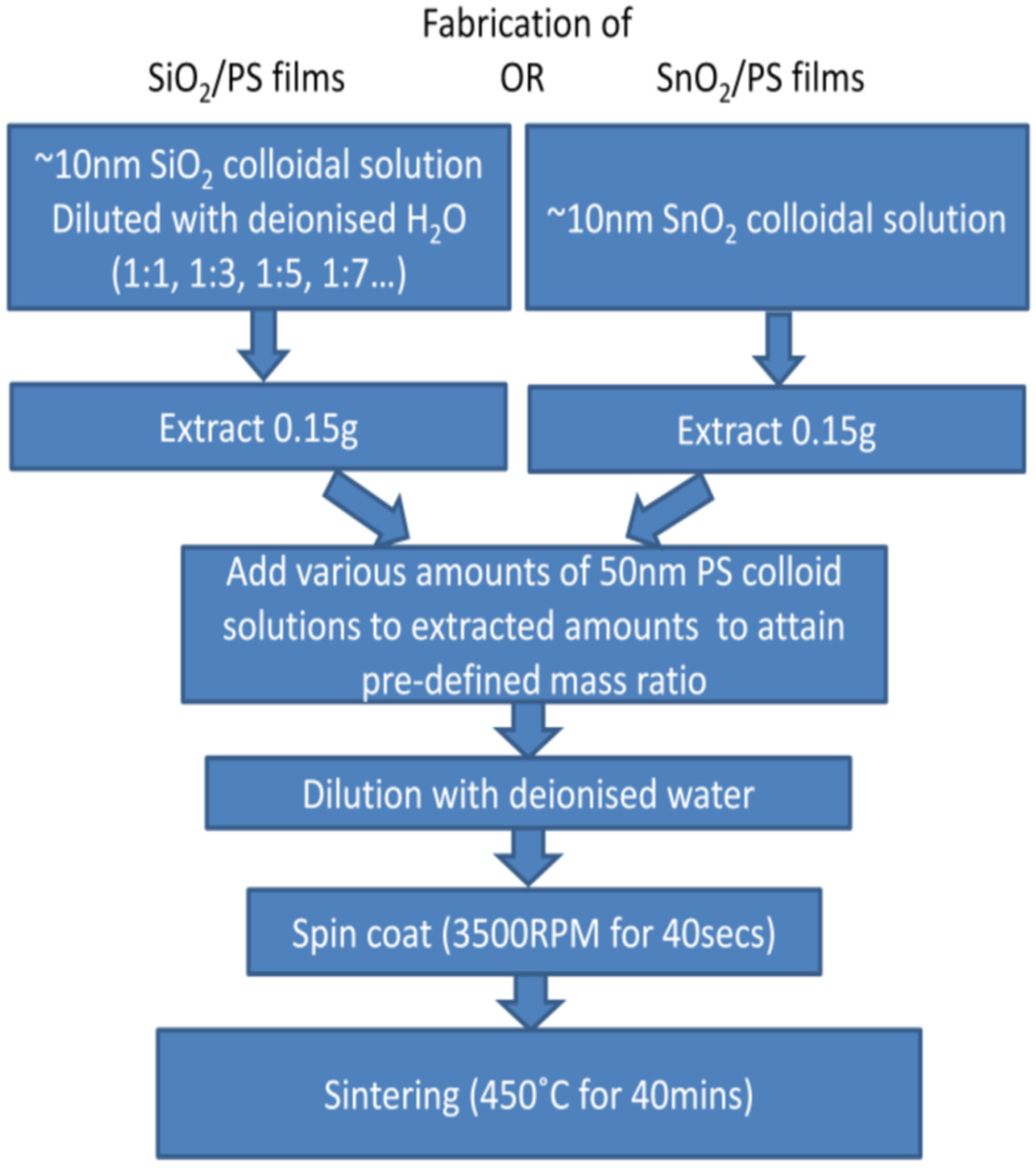
Before fabricating a multilayer stack, it is necessary to determine the amount of porosity required to obtain the required refractive index value. We induce porosity essentially by mixing 50 nm polystyrene spherical particles with 10 nm SiO2 or 10 nm SnO2 colloidal particle solutions, spin coat the mixture on a cleaned substrate and anneal it at high temperature to pyrolyse the polystyrene. The resulting layer is one of a porous network of SiO2 or SnO2 nanoparticles. More details on the fabrication method are provided in Appendix B.
3. Results
3.1. Optimized Anti-Reflection Multi-Layer
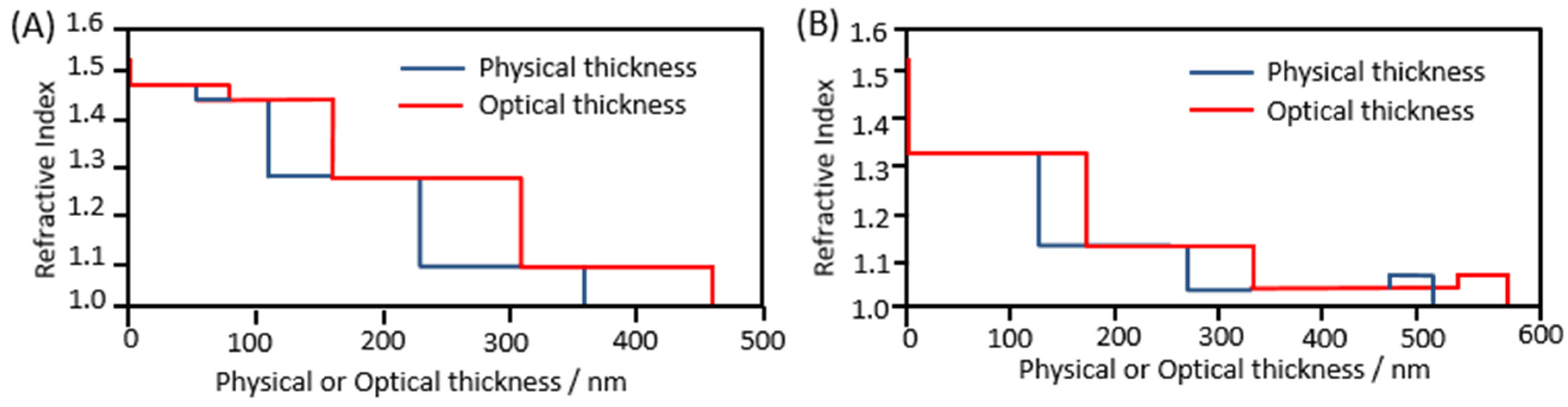
The conventional outlook on the most effective multilayer ARCs obliges a discretized continuous index profile that gradually reaches the ambient refractive index [7]. While many such index profiles were proposed, from simple linear equations to elaborate equations that require 5 factor terms to describe, they were not implemented widely due to the unavailability of materials with the necessary small changes in index [8,9,10]. However, with genetic algorithm optimization it may be possible to generate designs that can achieve high performance with only a few layers. A normal incidence optimized four-layer design is shown in Figure 2A while the angular incidence optimized four-layer design is shown in Figure 2B. The first design shows a conventional profile of a steadily decreasing index profile while the total optical thickness of 480 nm is approximately half a wavelength of the maximum incident wavelength. Its calculated average transmittance at normal incidence is 0.9545 and 0.896 over incident angles ranging from 0 to 80°. However, the second design shows a fourth layer that has an index higher than the third layer. Its calculated average transmittance of 0.9423 is lower than that of the first design at normal incidence but higher at 0.929 over all incident angles. Figure 3 shows the differences in performance of the two designs at every incident angle in TE and TM mode; the glass substrate reflectance is also shown as a comparison. A discussion utilizing the admittance loci representation provides the rationale for this unconventional design.
3.2. Admittance Loci Visualization
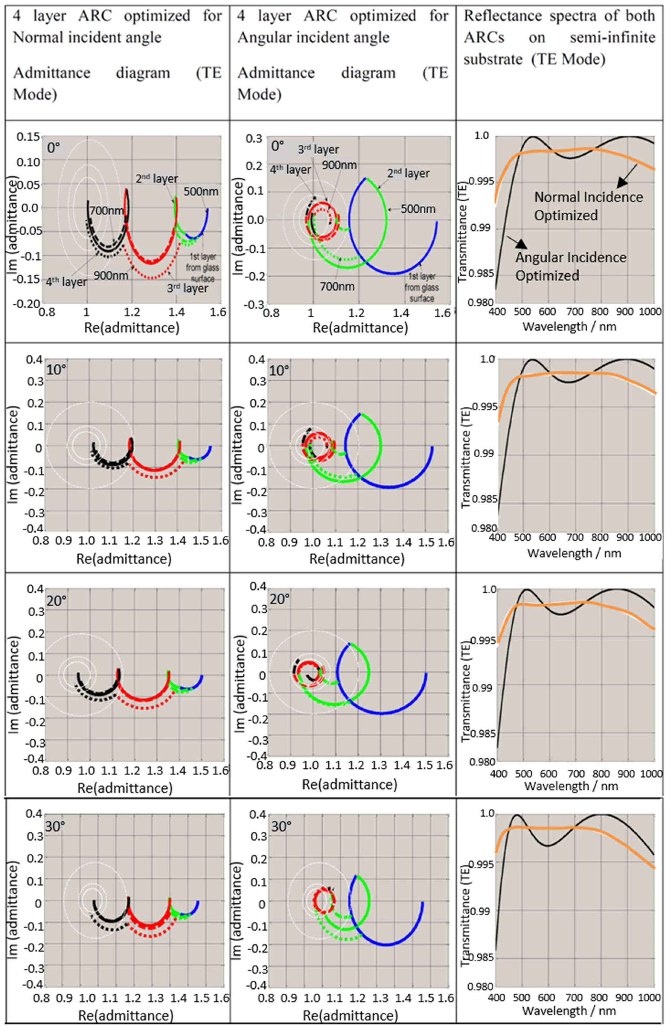
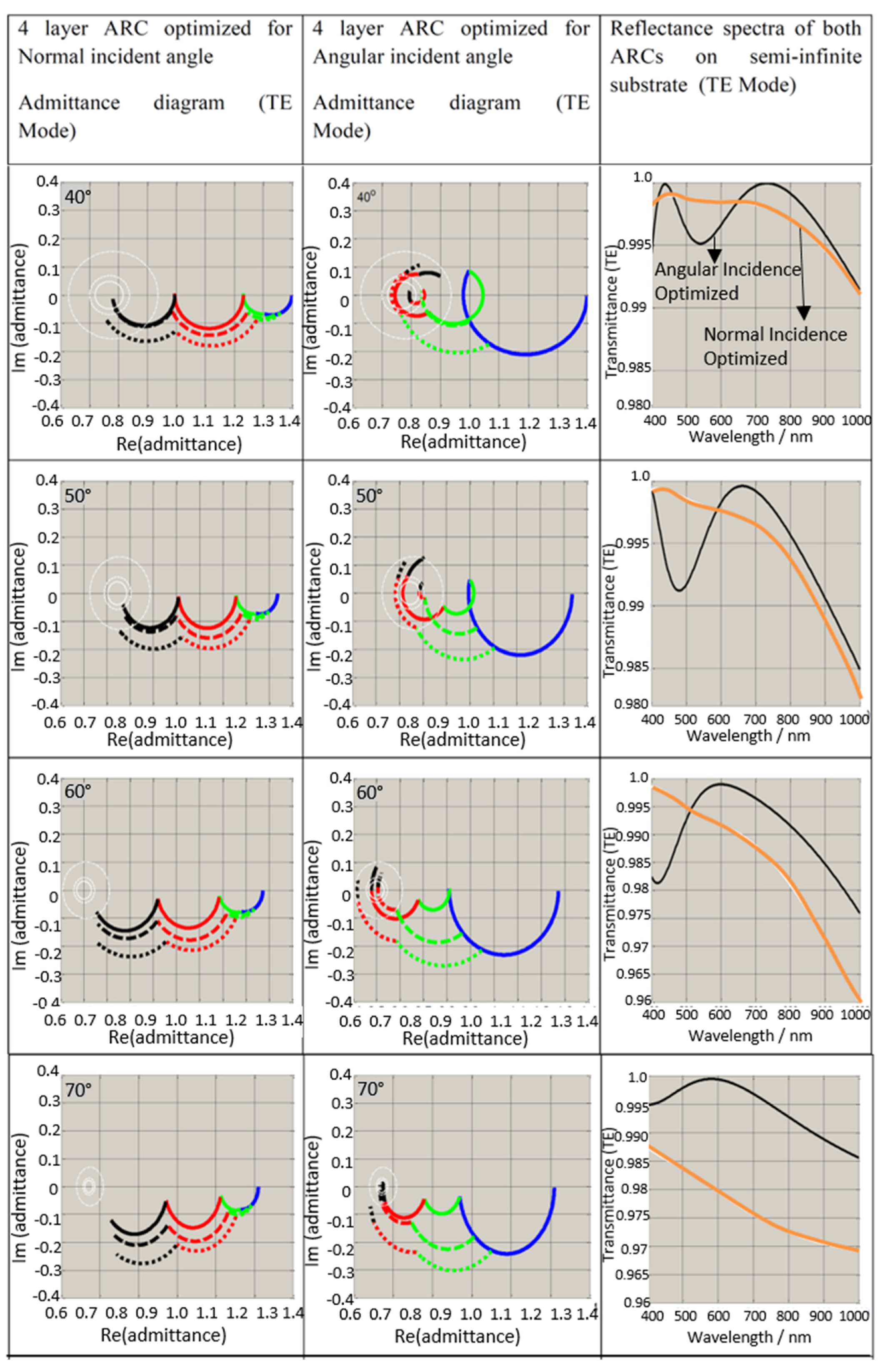
Figure 4 shows the admittance loci representations of the four-layer designs in TE mode (for the TM mode the visualization is given in Appendix A) and at 500 nm, 700 nm and 900 nm incident wavelengths. The blue arc indicates the first layer starting from the surface of the substrate with a real index 1.54, green the second layer, red the third layer and black the fourth layer. The solid arc indicates an admittance profile at an incident wavelength of 500 nm, the dashed arc at 700 nm, the dash-dot arc at 900 nm. The white circles indicate iso-reflectance circles with center (1,0) of 0.1% (solid), 0.2% (dashed), 1% (dot-dashed) reflectances. The iso-reflectance circles enlarge with increasing incident angles. The iso-reflectance contours in the 70° and 80° loci diagram for the normal incidence optimized ARC indicates 1%, 2% and 5%, and 15%, 20% and 25% reflectance, respectively, and iso-reflectance contours in the 80° loci diagram for the angular incidence optimized ARC are 15%, 20% and 25%.
The normal incidence optimized ARC at normal incidence has its third and fourth layer with optical thicknesses slightly greater than quarter wave, and its first and third layer together comprise nearly a quarter wavelength. The angular incidence optimized ARC loci consists of two loci which are each more than quarter wavelength thick, a third layer locus which is nearly half wavelength thick at short wavelengths (400–600 nm), and a fourth layer locus which has a small arc length. The third layer will act as an absentee layer at short wavelengths and the AR effect contributed by the third layer will be lost. This leads to a large refractive index difference between the fourth and second layer, with no intermediate step between them. Therefore, there is a smaller transmittance at short wavelengths, as shown in the transmittance spectra of the ARC on a semi-infinite substrate of index 1.54. Furthermore, the transmittance spectrum oscillates more significantly than the normal incidence optimized ARC. Hence, at the normal incident angle, the overall ARC performance of the angular incidence optimized ARC is worse than that of the normal incidence optimized ARC. However, at increasing incident angles, the effective optical thickness of each layer decreases as represented by the decrement in arc lengths for all wavelengths. For the loci at smaller wavelengths, the layers will appear optically thicker; hence the arc length of each layer at 500 nm wavelength will be larger than that at 700 nm wavelength, which in turn will be larger than that at 900 nm wavelength. The overall effect is to extend the end points of the admittance loci of the normal incidence optimized ARC to a point far from the zero-reflectance point, corresponding to an increasing reflectance with increasing angle of incidence at TE mode. However, for the angular incidence optimized ARC, the third layer’s locus arc length decreases with increasing incident angle such that the fourth layer locus extends its arc towards the zero reflectance point and not away from it. Hence, the end points of the four-layer loci are a smaller distance from the zero reflectance point than that of the normal incidence optimized ARC, which does not have sufficient thickness to compensate for the decrease in phase thickness with increasing incident angles. In summary, an unconventional design that does not strictly follow the conventional thinking of a decreasing refractive index profile is better optimized for all angles of incident transmittance.
4. Discussion
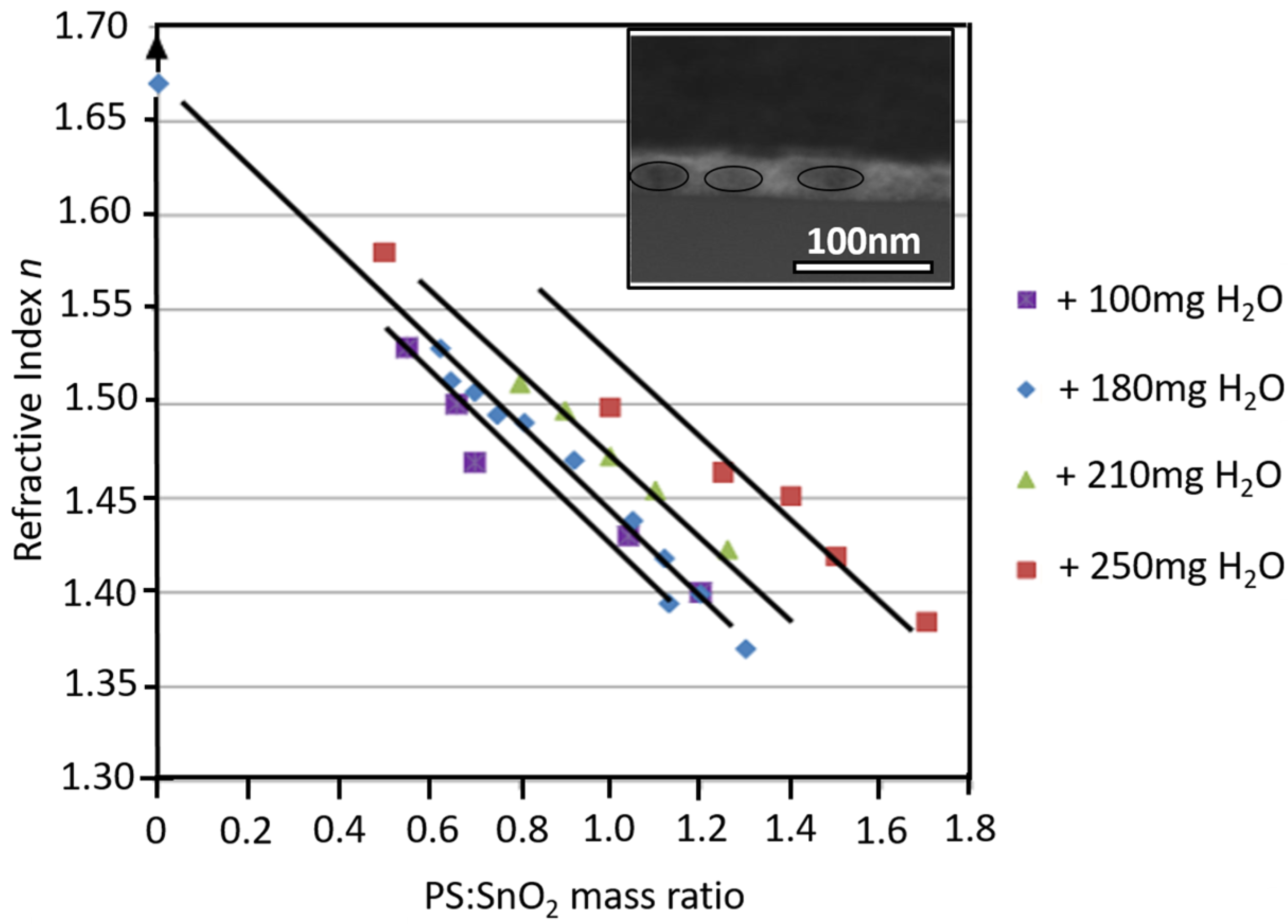
The ease of tuning the refractive index of a given material is illustrated in Figure 5 and Figure 6, where reduction in the refractive index of silicon oxide and tin oxide nanoparticle films [11] is achieved by increasing introduction of polystyrene particles. With the introduction of only a small amount of polystyrene in SiO2 nanoparticle solutions, the porosity induced by the removal of polystyrene is significant as seen by the steep drop in the refractive index. With increasing polystyrene, however, it becomes more difficult to achieve a very low refractive index as the change in index with further increase in porosity is gradual. The limit at which the internal framework of nanoparticles (hosting the induced porosity) can mechanically support itself becomes apparent as the index actually increases slightly at the largest polystyrene concentration. In Figure 5 inset, we determined the particle ratio of the SiO2 nanoparticles to the polystyrene nanoparticles from the density of the colloidal solution (1.22 g/mL, 30 wt % in H2O), density of the PS solution (0.025 g/mL, 2.5 wt % in H2O) and the dilution factor to arrive at ~1013 silica particles and ~109 PS particles in the prepared solution. In sum, it is relatively easy to induce an index drop of more than 0.3 for a silica nanoparticle film, but achieving an index of less than 1.1, which requires a packing fraction of only 10%, is difficult. However, it is conceivable that by improving the chemical adhesion between nanoparticles that a highly porous and mechanically robust scaffolding could be fabricated. For tin dioxide nanoparticle films, the trend is largely a linear decrease from an index of 3.5, and hence a combination of tin-dioxide and silica nanoparticle layered stack may be suitable for high index substrates such as silicon or ITO. From SEM cross sectional images, the PS generated voids tend to conglomerate into bigger and more elliptical voids within SnO2 particle films, whereas SiO2 particle films show an open network of SiO2 agglomerations.
With respect to a moth eye grating structure, this is limited by its mold template design, it is expensive to fabricate on a large scale of metric squared areas, and is not amenable to a wide variety of designs vis-à-vis every optical application or even every type of substrate such as polymeric substrates without having to make major changes to its fabrication process. Nanoparticle colloidal solutions, on the other hand, have been coated on polymeric substrates by making minor adjustments to its colloidal composition [12]. Furthermore, the necessarily precise gradual curvature of the conical moth eye nano-structures can be easily eroded and hence significantly lose its AR effectiveness. In contrast, by implementing a slightly thicker multilayer stack of 6 layers, the first 2 layers can be eroded and the performance of the ARC will still not suffer a major loss in its effectiveness. Although nanoparticle films may also have issues with mechanical robustness, its low cost of fabrication and ease of scalability can make it attractive for large scale optical applications that demand cost effectiveness, for example, the inside interface of a glass greenhouse.
One challenge in the fabrication of a stack of discrete nano-porous layers is that when spin coating or dip coating each colloidal solution sequentially, the colloidal layers will mix and form a single continuous layer. One successful solution lies in introducing a sacrificial layer of polystyrene particles on top of each colloidal layer, which can be pyrolyzed when all layers are coated, thus enabling discrete layers with different porosities (Figure 7). Another difficulty which is also inherent in other coating technologies is the heat treatment necessary to pyrolyze the polystyrene particles as well as forming a more mechanically stable coating. Even though a low heating temperature of 150 °C is sufficient to pyrolyze the polystyrene, it may still be difficult to implement on thermoplastic substrates such as PMMA. Therefore, other methods to remove polystyrene particles may be necessary. For example, we have observed that these polystyrene particles can also be easily removed by ozone, and therefore it may be possible to introduce a reactive gas that will remove these organics, and yet not harm the underlying substrate if it is well enveloped in a protective sleeve.
It may ultimately be necessary to pay attention to the optimal distribution of the nanoparticle packing in order to maximize mechanical robustness. Variables such as the size of the host nanoparticle and size of the pyrolyzable particles play a role, as well as deposition parameters. For example, Table 1 shows the effect of spin coating speed on the refractive index and thickness (characterized by ellipsometry) of a single layer of a mixture of SiO2 (diluted 1:15):PS = 1:5. It is clear that some variability in the index can be achieved by the spin coating speed. It is possible that with increasing RPM (Rotations Per Minute) the larger PS particles are more tightly compressed with the host silica film, and the rate of removal of PS versus silica solution is less when the rotational speed is high. The tighter compression may lead to a more interlinked porous network throughout the film. The final ratio of PS to silica after spin coating may also be greater. One characterization method for determining the characteristics of a porous film is the environmentally controlled ellipsometry, where the introduction of water moisture into the film and its removal can be studied through its change in the effective refractive index. Figure 8 shows the hysteresis curves [14] of the change in porosity as a function of increasing polystyrene (PS). If the film exhibits a large surface area due to an extensive porous network, its moisture content will be removed more rapidly as compared to a film with isolated porosity (for example, in a close-packed film of nano-spheres).
Further, other novel integrations can also be included in these porous networks. For example, one could introduce the use of hollow silica nanoparticles whereby the void fraction could be enhanced to achieve an even lower index. On the other hand, one could use close-packed calcined hollow spheres where the hollowness of the spheres could be utilized to effectively achieve the desired index and thus a more robust network. Yet another approach could be mixing of large hollow silica nanoparticles with small solid silica nanoparticles, with or without void inducing polystyrene particles, to achieve a desired combination of optical and structural properties.
5. Conclusions
The design and fabrication of multilayer ARCs using nanoparticles has the potential to impact industrial methods and processes. We present the optimal configuration of such a stack and discussed its rationale for effective anti-reflective performance. The solution for preparing such a stack is also discussed and it is shown that, with creative ways of removing the pryolyzable material, the entire process is amenable to various substrates. This field hence has great potential to grow as long as its technological difficulties can be surmounted in a cost-effective method.
Acknowledgments
The authors acknowledge the support of the Ontario Research Fund—Research Excellence program and the Natural Sciences and Engineering Research Council Canada.
Author Contributions
Joel Yi Yang Loh fabricated, characterized and coded all work shown in this article. Joel Yi Yang Loh and Nazir Kherani prepared the article.
Conflicts of Interest
The authors declare no conflict of interest.
Appendix A

Table A1.
Matrices used to calculate optimized Transmittance/reflectance.
| TE Polarization | TM Polarization |
|---|---|
| Matrix of a single layer M, with thickness d, refractive index n at an incident angle | |
| Matrics of a stack, Mstack for the product sum of the matrics of j sub-layers of d thickness | |
| Expressions for field transmission and reflection coefficients | |
| Intensity coefficients for a film on a semi-infinite substrate | |
| ; | |
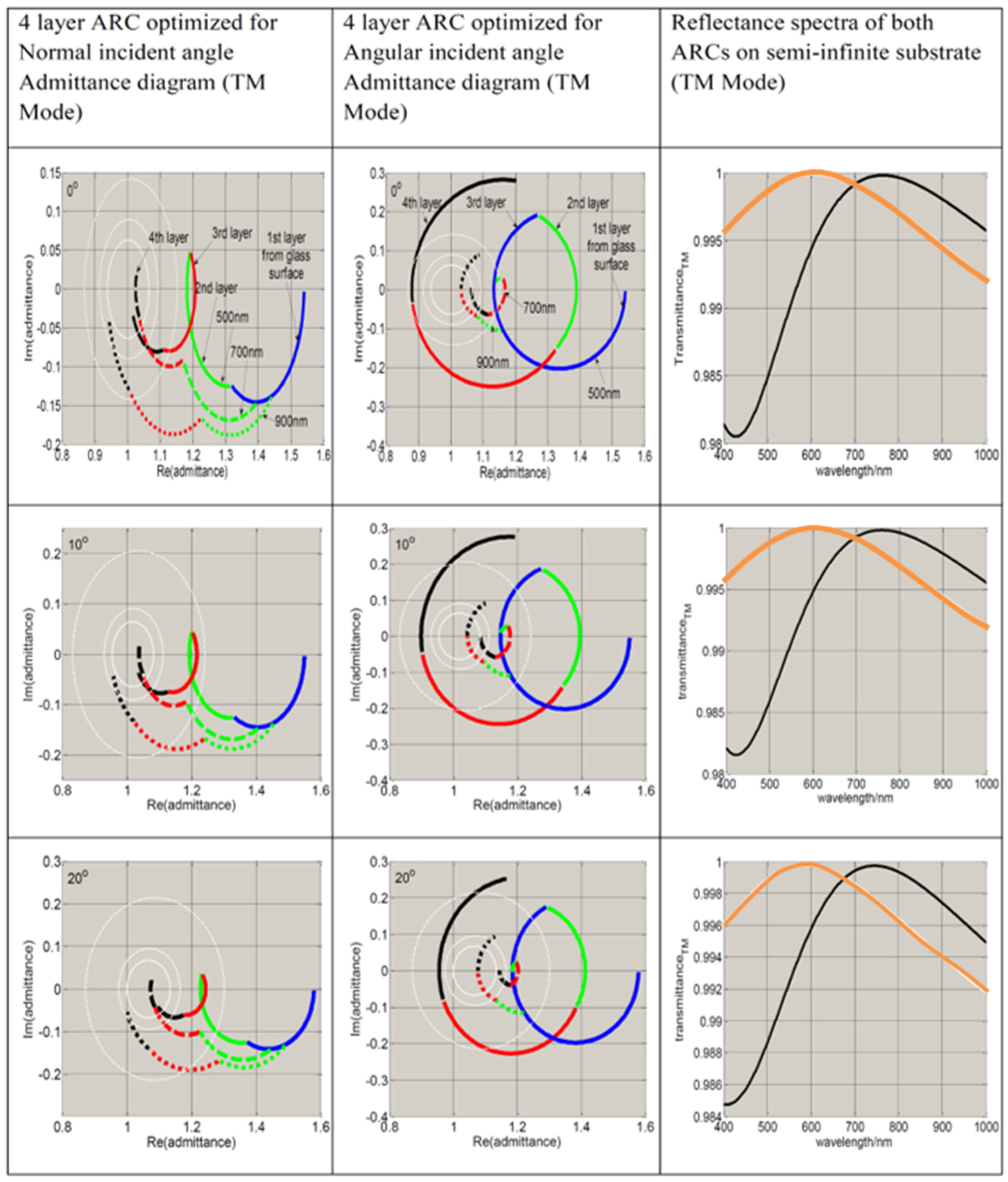
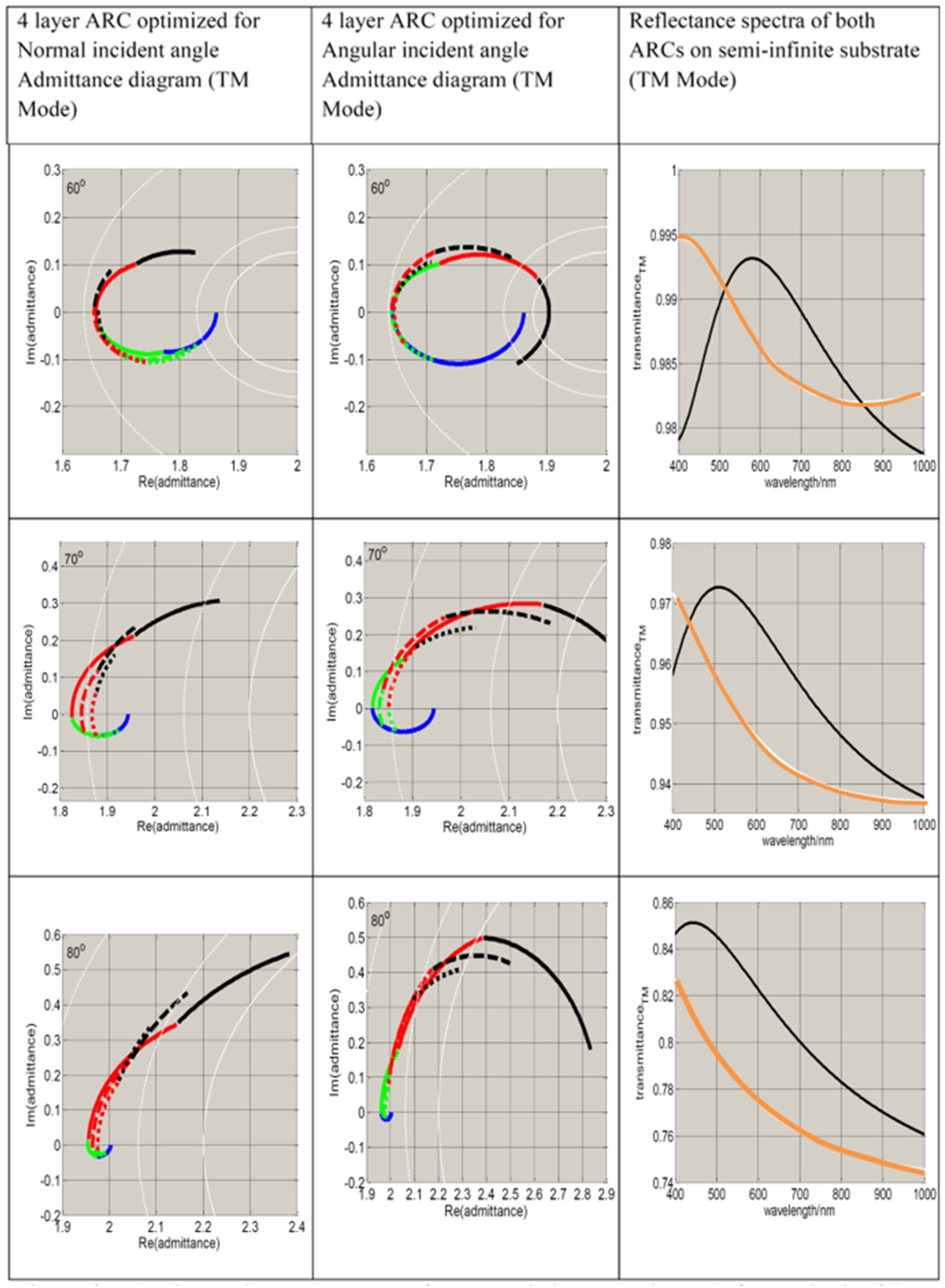
Figure A1.
Admittance loci for the normal incidence optimized and angular incidence optimized ARC designs for TM mode. The TM transmittance spectra for these designs on a semi-infinite glass substrate are also shown. The admittance loci representations are shown for increasing angles of incidences from 0° to 80°.

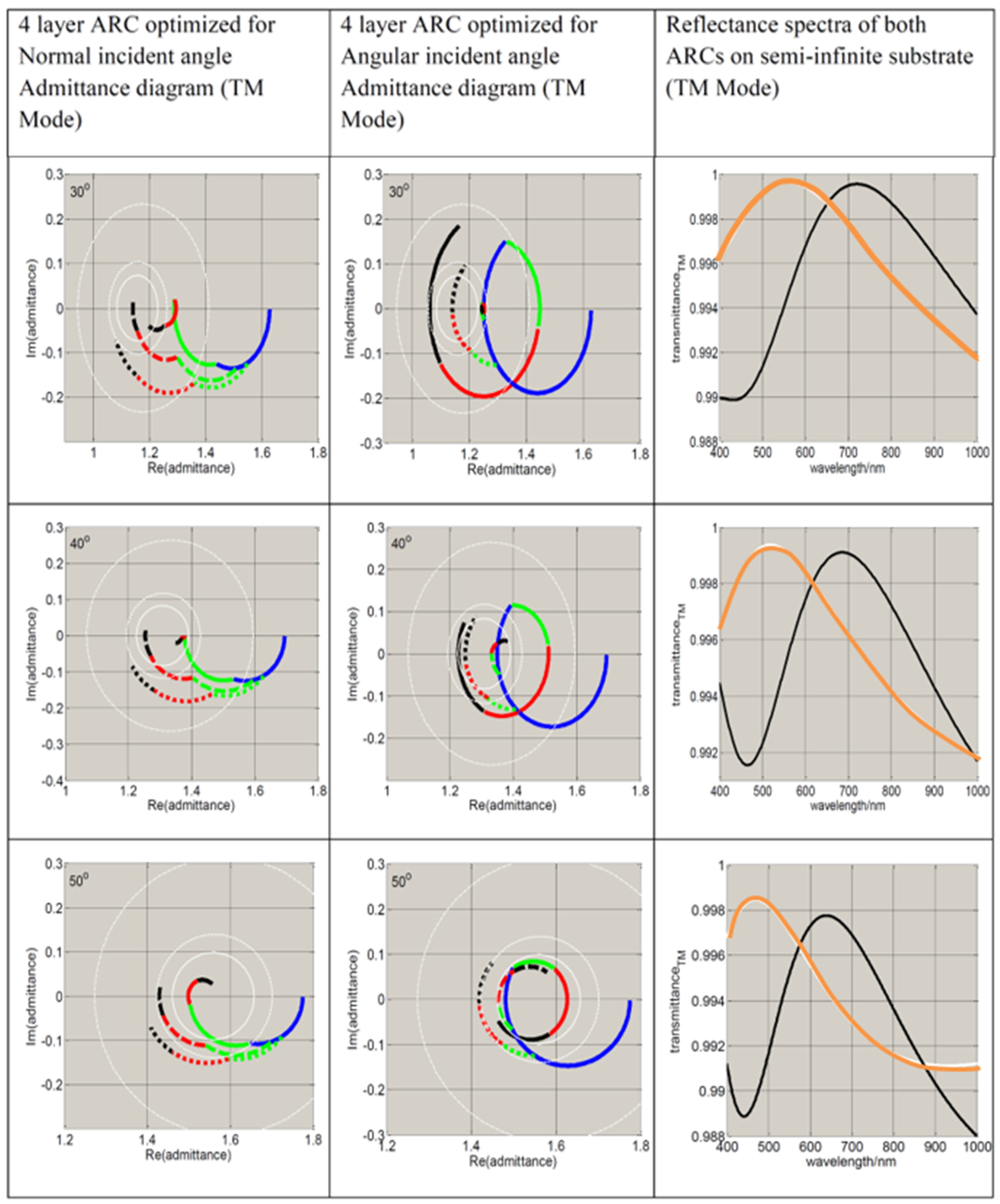

Admittance diagram for TM mode optimized for four-layer ARCs for normal incident angle and angular incident angles shown above. The admittance loci at TM mode are obviously similar to the loci at TE mode at normal incident angle. As the incident angle increases, the end points of the loci stay within the low reflectance loci as indicated by the white circles until an angle of 60°, the end points at 70° and 80° which then begin to extend away from the zero reflectance point indicated by the centre of the iso reflectance circles. At 60° and 70°, the normal incidence optimized ARC loci does not have sufficient effective phase thickness such that the end points extend to the zero reflectance point, whereas the angular incidence optimized ARC has its first layer optically thick up to nearly a quarter wavelength at 70°, and the rest of the layer loci extend further than the normal optimized ARC loci into the zero-reflectance point.
Appendix B
The SiO2 colloidal solution is first diluted with H2O: For example, 1 g of SiO2 solution is diluted with 1 g of deionized H2O to prepare SiO2 (1:1 dilution). In the next step, 0.015 g of SiO2 solution is extracted from the diluted solution and mixed with varying mass of polystyrene (PS) colloidal solution. The mass ratio indicated in the following data refers to the ratio of the mass of PS solution with the 0.015 g mass of diluted SiO2 solution. As the volume of the solutions of PS/SiO2 is too small to enable uniform coating of a 1 inch by 1 inch substrate, or for multiple samples, it is necessary to dilute the preceding solutions with 100 mg H2O to increase the overall volume. For SnO2, 0.015 g of SnO2 solution is extracted and mixed with varying mass of PS solution. Hence the mass ratio indicated in the following data refers to the ratio of the mass of PS solution with the 0.015 g mass of SnO2 solution which is not yet diluted. The PS/SnO2 solutions are then diluted with varying mass of deionized H2O.
Figure A1.
The process for making SnO2 particle or SiO2 particle films.

The solutions of SiO2 and SnO2 with different polystyrene (PS) mass ratios were spin coated at an RPM of 3500 for 40 s, and sintering at 450 °C for 40 min. The refractive index (at 633 nm wavelength) and thickness of a single layer is obtained by spin coating on a silicon substrate and characterized via spectral ellipsometry. Regression analysis using a Cauchy law dispersion formula with a single Lorentz peak was conducted using WINELLI 2.
References
- Raut, H.K.; Ganesh, V.A.; Nair, A.S.; Ramakrishna, S. Anti-reflective coatings: A critical, in-depth review. Energy Environ. Sci. 2011, 4, 3779–3804. [Google Scholar] [CrossRef]
- Sun, C.H.; Jiang, P.; Jiang, B. Broadband moth-eye antireflection coatings on silicon. Appl. Phys. Lett. 2008, 92. [Google Scholar] [CrossRef]
- Wilson, S.J.; Hutley, M.C. The optical properties of “moth eye” antireflection surfaces. Opt. Acta Int. J. Opt. 1982, 29, 993–1009. [Google Scholar] [CrossRef]
- Ji, S.; Song, K.; Nguyen, T.B.; Kim, N.; Lim, H. Optimal moth eye nanostructure array on transparent glass towards broadband antireflection. ACS Appl. Mater. Interfaces 2013, 5, 10731–10737. [Google Scholar] [CrossRef] [PubMed]
- MacLeod, H.A. Thin-Film Optical Filters; CRC Press: Boca Raton, FL, USA, 1969. [Google Scholar]
- Poxson, D.J.; Schubert, M.F.; Mont, F.W.; Schubert, E.F.; Kim, J.K. Broadband omnidirectional antireflection coatings optimized by genetic algorithm. Opt. Lett. 2009, 34, 728–730. [Google Scholar] [CrossRef] [PubMed]
- Xi, J.Q.; Schubert, M.F.; Kim, J.K.; Schubert, E.F.; Chen, M.; Lin, S.Y.; Liu, W.; Smart, J.A. Optical thin film materials with low refractive index for broadband elimination of Fresnel reflection. Nat. Photonics 2007, 1, 176–179. [Google Scholar]
- Jacobsson, R. Light reflection from films of continuously varying refractive index. Prog. Opt. 1966, 5, 249–284. [Google Scholar]
- Yeh, P.; Sari, S. Optical properties of stratified media with exponentially graded refractive index. Appl. Opt. 1983, 22, 4142–4145. [Google Scholar] [CrossRef] [PubMed]
- Southwell, W.H. Gradient-index antireflection coatings. Opt. Lett. 1983, 8, 584–586. [Google Scholar] [CrossRef] [PubMed]
- Yancey, S.E.; Zhong, W.; Heflin, J.R.; Ritter, A.L. The influence of void space on anti-reflection coatings of silica nanoparticle self-assembled films. J. Appl. Phys. 2006, 99. [Google Scholar] [CrossRef]
- Szymczyk, K.; Zdziennicka, A.; Jańczuk, B.; Wójcik, W. Wettability of polymeric solids by aqueous solution of surfactants. Langmuir 2007, 23, 8740–8746. [Google Scholar] [CrossRef] [PubMed]
- Loh, J.Y.; Puzzo, D.P.; O’Brien, P.G.; Ozin, G.A.; Kherani, N.P. Enhancing photovoltaics with broadband high-transparency glass using porosity-tuned multilayer silica nanoparticle anti-reflective coatings. RCS Adv. 2014, 4, 31188–31195. [Google Scholar] [CrossRef]
- Sing, K.S.W. Reporting physisorption data for gas/solid systems with special reference to the determination of surface area and porosity. Pure Appl. Chem. 1985, 57, 603–619. [Google Scholar] [CrossRef]
Figure 1.
Enhanced transmittance spectrum of a PMMA substrate coated with a single layer of silica nanoparticles in contrast to an uncoated PMMA substrate. The silica particles are FCC close packed. The calculated transmittance of a single layer with physical thickness of 150 nm and refractive index 1.33 shows a match with the experimental results.
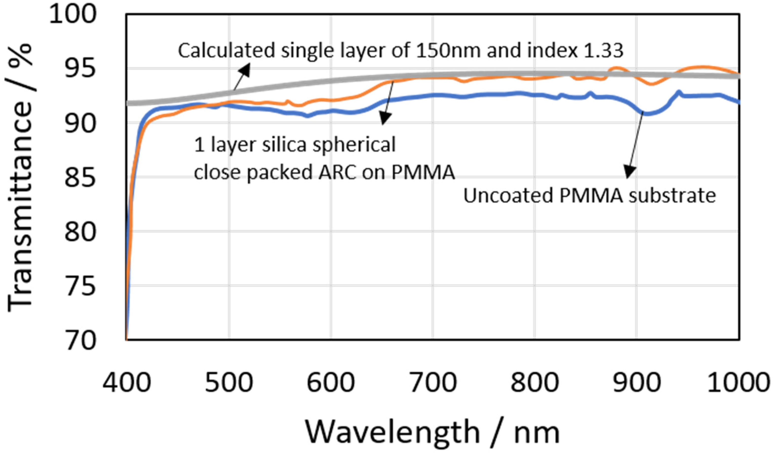
Figure 2.
Two designs generated by G.A optimiz for 0° angle incidence (A), and 0–80° angle incidence (B). The first design follows a conventional index profile, while the second design has a thick low index third layer and a higher index fourth layer.
Figure 2.
Two designs generated by G.A optimiz for 0° angle incidence (A), and 0–80° angle incidence (B). The first design follows a conventional index profile, while the second design has a thick low index third layer and a higher index fourth layer.

Figure 3.
The TE mode and TM mode reflectance profiles of both anti-reflection coating (ARC) designs. The angular incidence optimized design has significantly lower reflectance than the normal incidence optimized design at 70° and 80° incidence.
Figure 3.
The TE mode and TM mode reflectance profiles of both anti-reflection coating (ARC) designs. The angular incidence optimized design has significantly lower reflectance than the normal incidence optimized design at 70° and 80° incidence.

Figure 4.
Admittance loci for the normal incidence optimized and angular incidence optimized ARC designs for TE mode. The TE transmittance spectra for these designs on a semi-infinite glass substrate are also shown. The black and orange lines represent angular and normal incidence optimized designs respectively. The admittance loci representations are shown for increasing angles of incidences from 0° to 70°.


Figure 5.
The index trend of SiO2 nanoparticle films with increasing polystyrene solution mass ratio. There are two distinct trends, a sharp decrease in index with minimal introduction of PS, and a gradual decrease in index with significant introduction of PS. Inset: the refractive indices as a function of the estimated PS–SiO2 particle ratio. Reproduced from [13] with permisson (Copyright Royal Society of Chemistry 2014). The other inset shows the cross-sectional SEM image of the void filled silica particle film.
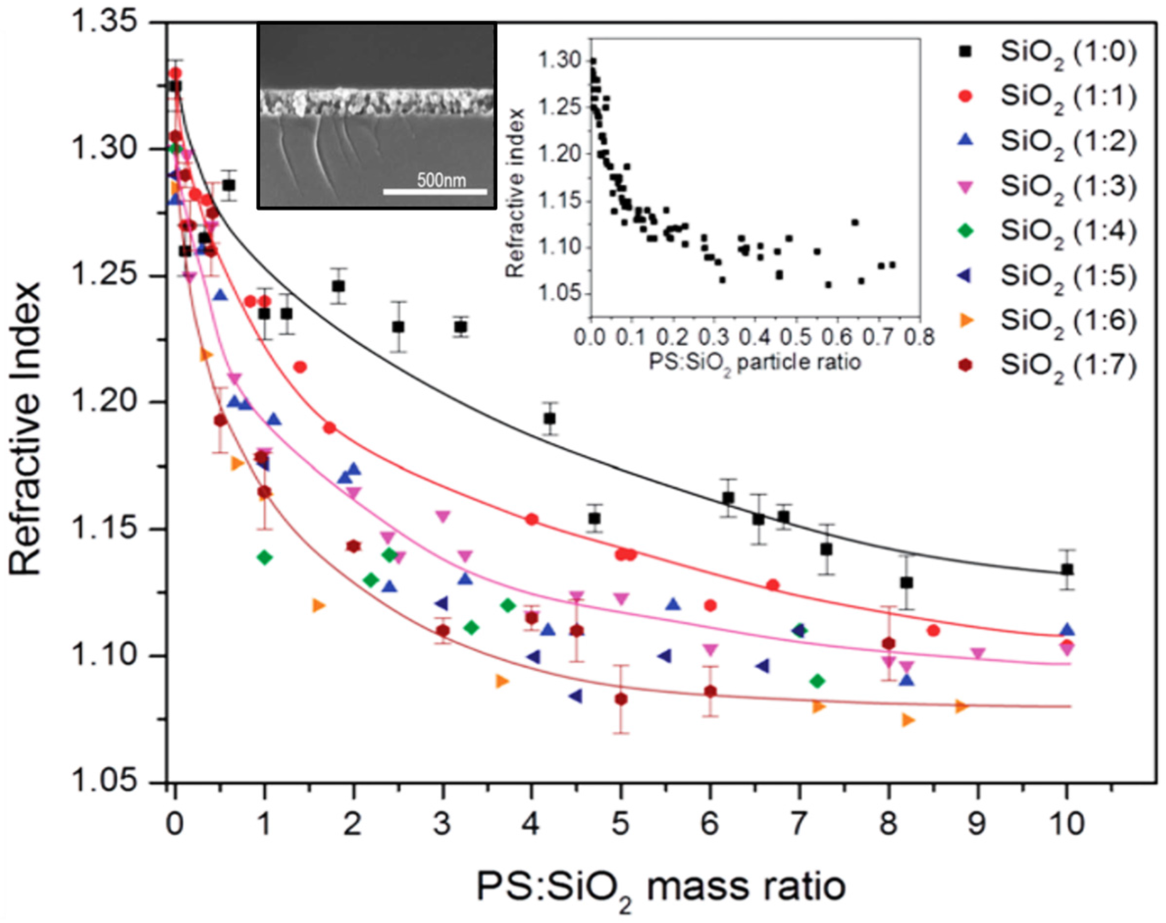
Figure 6.
The linear index trend of SnO2 nanoparticle films at increasing water solvent dilution with increasing polystyrene solution mass ratio. The inset shows a cross sectional SEM image of the void filled SnO2 particle film. The ellipses indicate the conglomeration of the voids.
Figure 6.
The linear index trend of SnO2 nanoparticle films at increasing water solvent dilution with increasing polystyrene solution mass ratio. The inset shows a cross sectional SEM image of the void filled SnO2 particle film. The ellipses indicate the conglomeration of the voids.

Figure 7.
Sequence of steps to fabricate a discrete multilayer with graded refractive index.
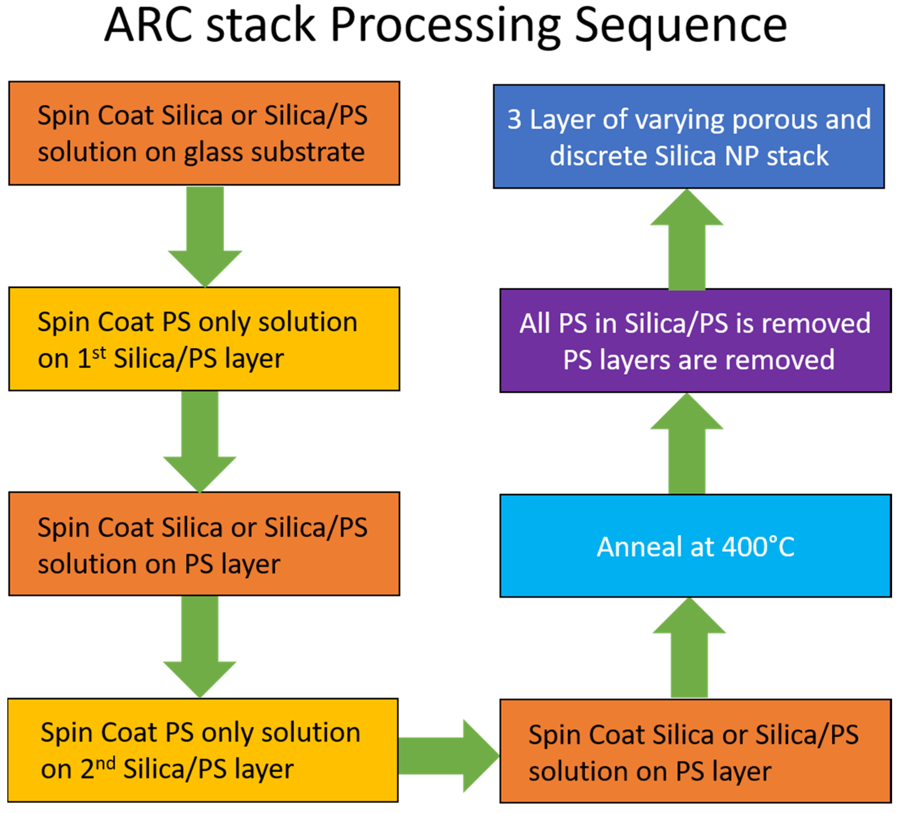
Figure 8.
Porosimetry isotherms for 1:3 diluted SiO2 nanoparticles with increasing polystyrene (PS) ratio.
Figure 8.
Porosimetry isotherms for 1:3 diluted SiO2 nanoparticles with increasing polystyrene (PS) ratio.
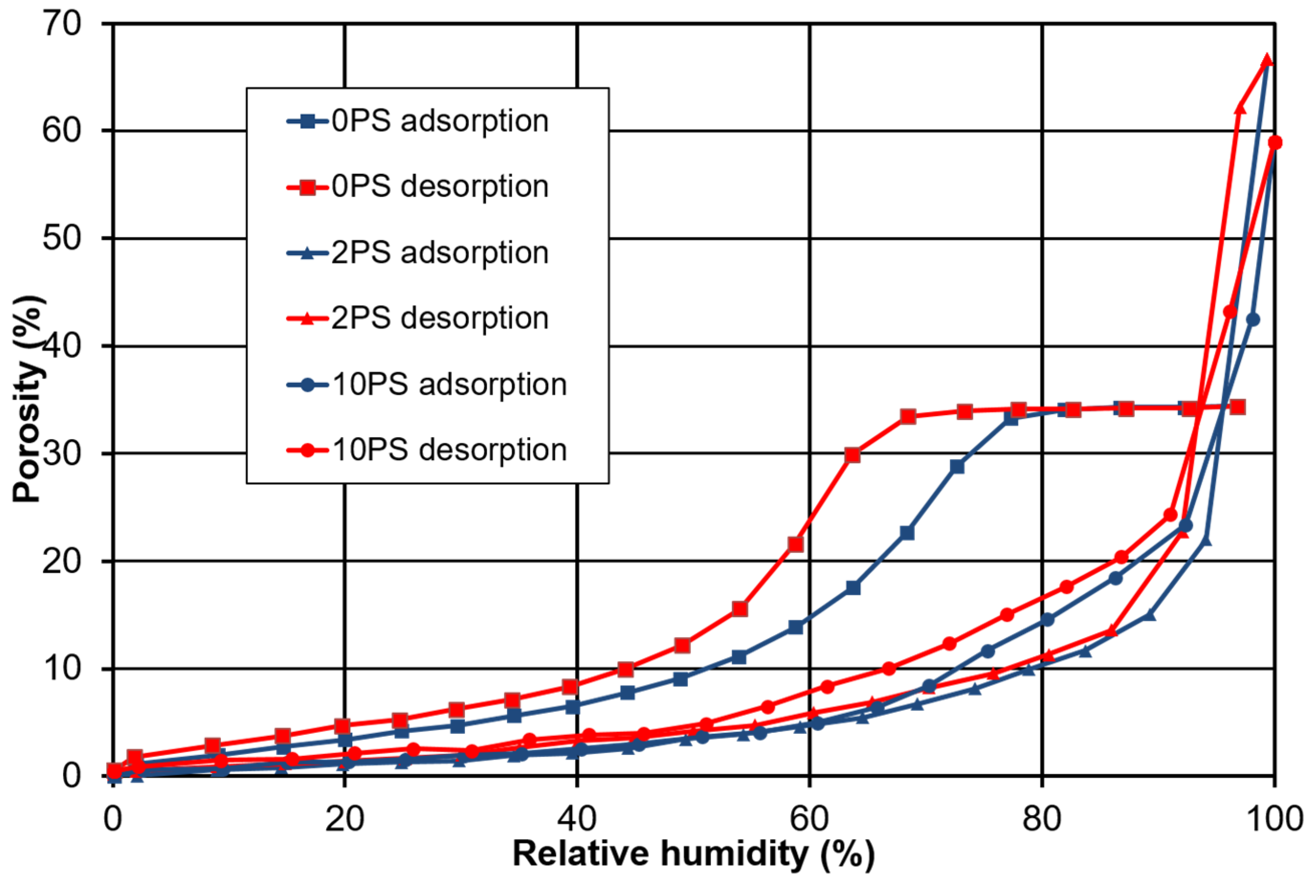
Table 1.
The thickness and refractive index as measured by ellipsometry as a function of spin rate in RPM. As the spin rate decreases, the thickness decreases and the refractive index increases.
Table 1.
The thickness and refractive index as measured by ellipsometry as a function of spin rate in RPM. As the spin rate decreases, the thickness decreases and the refractive index increases.
| Max Rotational Speed/RPM | Thickness/nm | Refractive Index |
|---|---|---|
| 3500 | 47.9 | 1.093 |
| 1000 | 58.2 | 1.121 |
| 500 | 64.9 | 1.141 |
© 2017 by the authors. Licensee MDPI, Basel, Switzerland. This article is an open access article distributed under the terms and conditions of the Creative Commons Attribution (CC BY) license (http://creativecommons.org/licenses/by/4.0/).
Share and Cite
MDPI and ACS Style
Loh, J.Y.Y.; Kherani, N. Design of Nano-Porous Multilayer Antireflective Coatings. Coatings 2017, 7, 134. https://doi.org/10.3390/coatings7090134
AMA Style
Loh JYY, Kherani N. Design of Nano-Porous Multilayer Antireflective Coatings. Coatings. 2017; 7(9):134. https://doi.org/10.3390/coatings7090134
Chicago/Turabian StyleLoh, Joel Yi Yang, and Nazir Kherani. 2017. "Design of Nano-Porous Multilayer Antireflective Coatings" Coatings 7, no. 9: 134. https://doi.org/10.3390/coatings7090134
Note that from the first issue of 2016, this journal uses article numbers instead of page numbers. See further details here.