Epitaxial Growth of AlN on (0001) Sapphire: Assessment of HVPE Process by a Design of Experiments Approach

 and
and
Abstract
:1. Introduction
- Running three times the same experiment on a central working recipe with fixed 15 parameters to quantify the error on various responses (detailed below);
- Running 16 experiments following levels indicated by an Hadamard matrix of order 16 for each parameter and measuring the responses;
- Running 1 additional experiment on the central working recipe (to assess any shifting of process) and one final experiment with all the parameters in a configuration out of Hadamard matrix to assess the robustness of the simple linear model obtained.
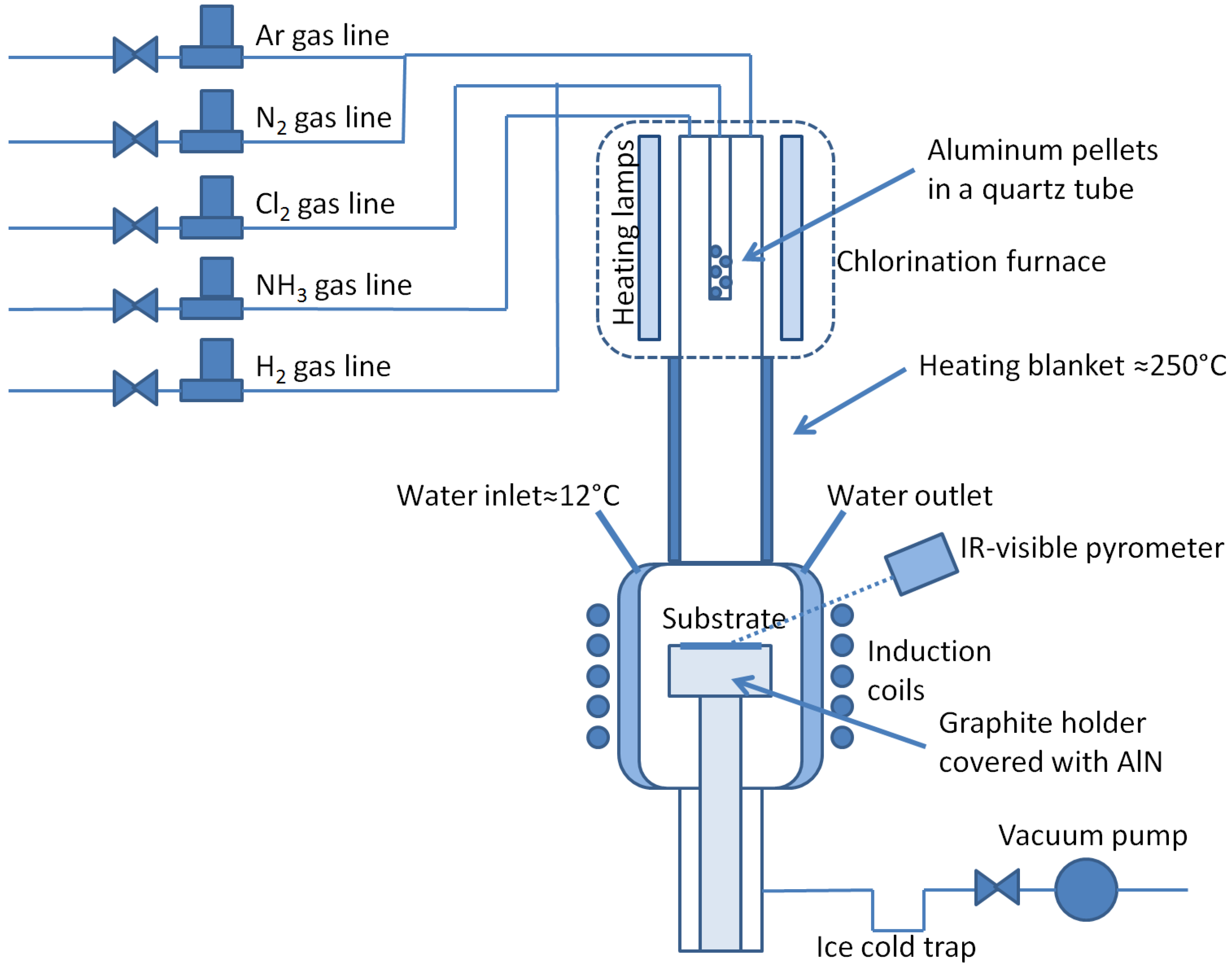
2. Method
- The chlorination furnace is loaded with the same mass of aluminum pellets 5 or 10 mm in diameter (discrete parameter) and the substrate is loaded out of the box (no further cleaning) into the reactor body under vacuum few minutes or the day before experiments (discrete parameter to assess the effect of room temperature desorption); The aluminum pellets can be new or used once in a preceding experiment (discrete parameter).
- The reactor vessel is purged three times with argon at room temperature.
- The aluminum load is cleaned under hydrogen (200 sccm) for a time varying from 0 to 30 min at a temperature fixed by the furnace power varying from 40% to 50%, corresponding to a temperature for the aluminum pellets in the approximate range 500–600 °C.
- The pressure into the reactor is set (1330 to 2660 Pa or 10 to 20 torrs) and the flow rate of hydrogen is set to a value varying from 3.72 × 10⁻⁴, to 1.12 × 10⁻³ mol·s−1 (500 to 1500 sccm).
- The temperature is ramped-up at 2%/min of the induction coil power (temperature increase of the substrate around 20 °C/min).
- The substrate is cleaned at 1100 °C under hydrogen for a time varying from 0 to 20 min.
- The temperature is ramped-up again at 2%/min of the induction coil power toward the deposition temperature (1200 to 1300 °C).
- Cl2 (2 sccm or 1.49 × 10⁻⁶ mol·s−1) is injected into the chlorination tube from 0 to 2 min prior to NH3 to tentatively favor Al polarity; this step is called “pre-chlorination”.
- Cl2 and NH3 flow rates are set to their set points (2 sccm Cl2, 1.33 to 3.99 sccm NH3 or 9.90 × 10⁻⁷ to 2.97 × 10⁻⁶ mol·s−1, N/Al ratio in gas phase ranging from 1 to 3).
- Reactants are sequentially injected, AlCl3 for one second then purge then NH3 for one second then purge, or simultaneously injected, both at the same time for one second then purged (discrete parameter), with purge times varying from 0 to 4 s (the growth mode consequently ranging from pure “ALD-like” mode (atomic layer deposition, sequential injection with purges in-between) to CVD (simultaneous injection without purge) passing by pulsed or modulated CVD (simultaneous injection with purges or sequential injection without purges). The intake time of reactants (NH3 and AlCl3) is set to 1000 s each, so that the total mole quantity of reactants entering the reactor is kept constant between depositions.
- The gas phase is then changed to pure N2 or H2 + 1%NH3, keeping the same flow rate (discrete parameter).
- The temperature is ramped-down at 1%/min or 3%/min of the induction coil power toward 600 °C.
- Final cooling down to room temperature is performed with 1000 sccm Ar.
- Sample is unloaded and reactor tube is finally cleaned with 5% HCl in deionized water, then deionized water, then isopropanol. Tube is finally dried under vacuum before next experiment.
- Raman Shift in cm−1 of the E2(h) peak of AlN measured far from cracks with a Renishaw In-Via spectrometer (Renishaw, Wotton-under-Edge, Gloucestershire, UK) and a 10 mW Ar+-laser with 514 nm wavelength. The shift is averaged on 12 measurements covering the full wafer with spot diameter ≈1 µm.
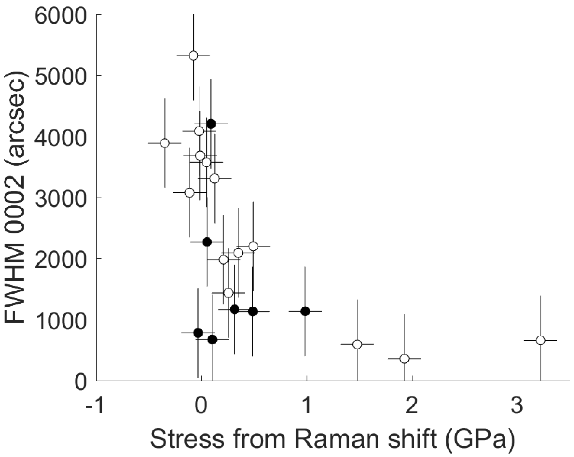
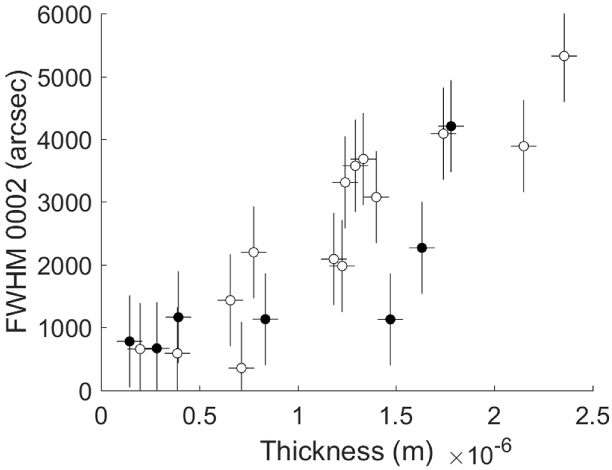
- FWHM (Full Width at Half Maximum) of E2(h) peak of AlN measured far from cracks and averaged on 12 measurements covering the full wafer. This should be representative of the quality of AlN layer.
- Radius of curvature of the sample (in m−1) measured by a Talysurf Mechanical profilometer (Ametek Inc, Berwyn, PA, USA). Orthogonal cross measurements of the whole sample were averaged.
- FWHM of the 0002 reflection peak of AlN measured by XRD measurements in ω-scan. Such measurements were performed in PANalytical X’Pert PRO powder diffractometer (PANalytical, Almelo, The Netherlands) using Cu Kα1,2 radiation.
- Thickness in nm measured by optical ellipsometry (ellipsometer Accurion, Nanofilm EP3 SE, Accurion GmbH, Goettingen, Germany).
- RA (arithmetic average) and RMS (root mean square) roughness measured by AFM (Atomic Force Microscopy). AFM measurements were performed using NanoScope Dimension 3100 (Bruker France S.A.S, Palaiseau, France) in tapping mode. The roughness are measured far from surface cracks and averaged on several scanning area of 10 µm × 10 µm.
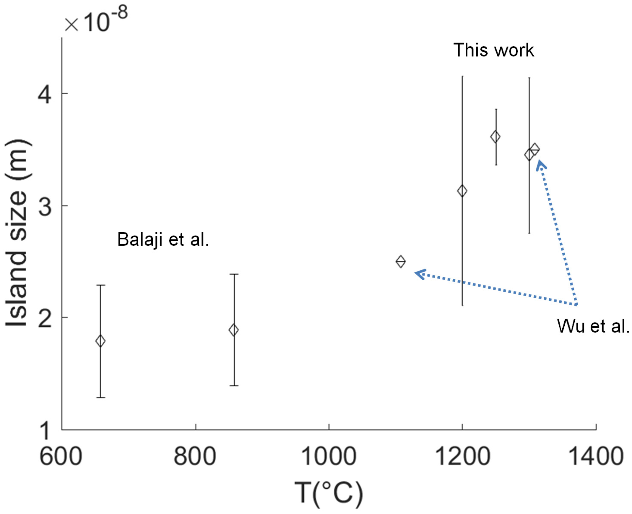
- Finally, the size of primary nucleation islands is calculated from the stress state of the AlN layer measured at room temperature by the Raman shift or the radius of curvature.
3. Results
4. General Discussion on the Effect of Process Parameters
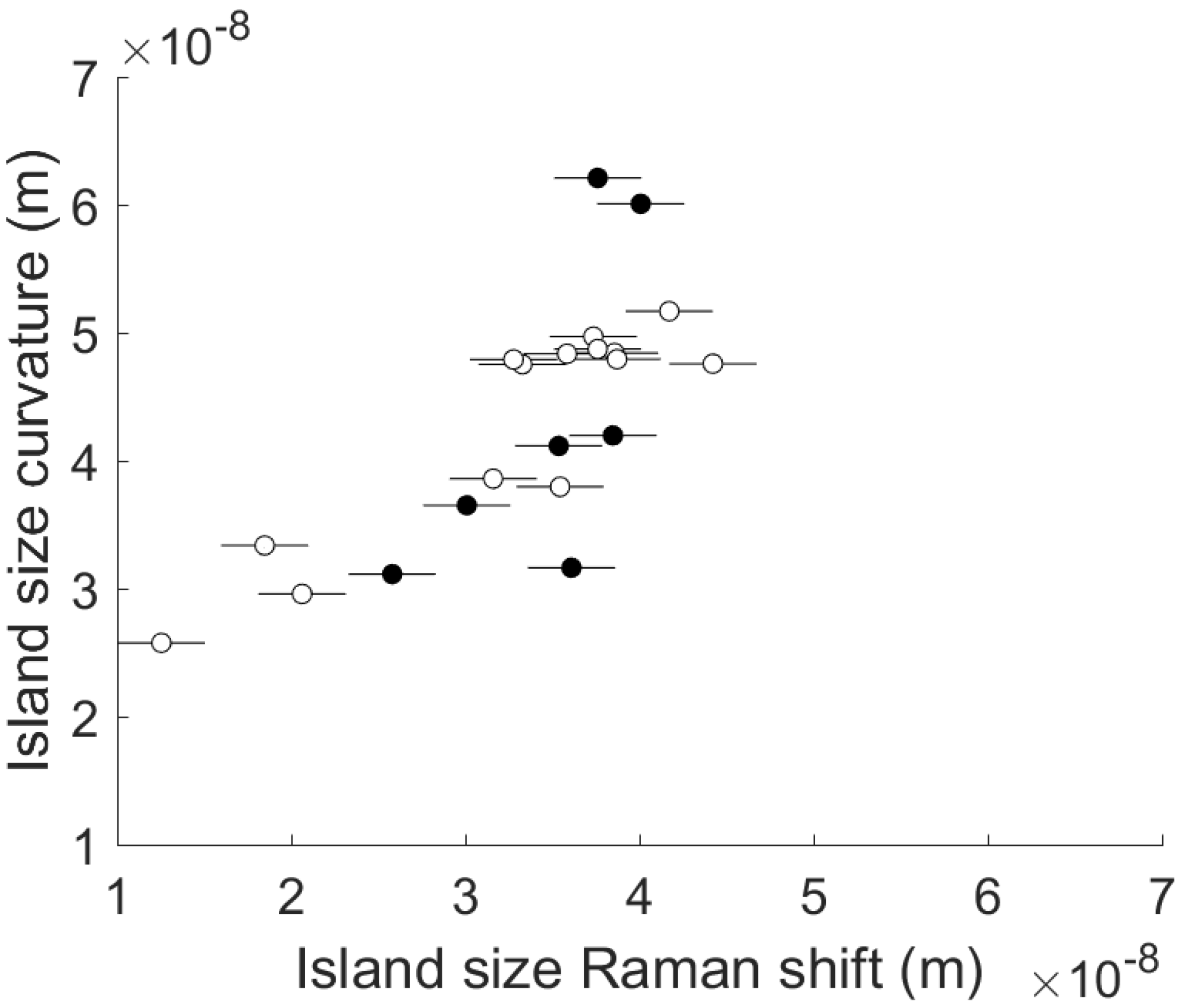
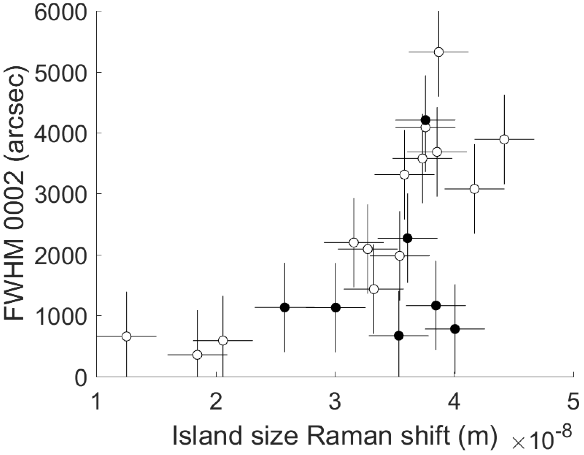
5. Correlation between Responses
- Cold wall reactors must have controlled wall temperature, as high as possible with available cooling fluid to avoid condensation and uncontrolled release of species.
- Robust method must be used to reveal driving growth parameters. Uncontrolled or considered as secondary parameters can overtake the recipe parameters. None of the growth parameters in CVD should be considered as secondary.
- CVD deposited layers can present very contrasted stress states that are mainly related to the coalescence step. Control of the early steps of growth is critical for stress management in grown layers, but also for aiming a good crystal quality.
6. Summary
Acknowledgments
Author Contributions
Conflicts of Interest
References
- Strite, S.; Morkoç, H. GaN, AlN, and InN: A review. J. Vac. Sci. Technol. B Microelectron. Nanometer Struct. 1992, 10, 1237–1266. [Google Scholar] [CrossRef]
- Peng, B.; Gong, D.; Zhang, W.; Jiang, J.; Shu, L.; Zhang, Y. Effects of sputtering parameters on AlN film growth on flexible hastelloy tapes by two-step deposition technique. Materials 2016, 9, 686. [Google Scholar] [CrossRef] [PubMed]
- Aissa, K.A.; Elmazria, O.; Boulet, P.; Aubert, T.; Legrani, O.; Mangin, D. Investigations of AlN thin film crystalline properties in a wide temperature range by in situ X-ray diffraction measurements: Correlation with AlN/Sapphire-based SAW structure performance. IEEE Trans. Ultrason. Ferroelectr. Freq. Control 2015, 62, 1397–1402. [Google Scholar] [CrossRef] [PubMed]
- Kano, K.; Arakawa, K.; Takeuchi, Y.; Akiyama, M.; Ueno, N.; Kawahara, N. Temperature dependence of piezoelectric properties of sputtered AlN on silicon substrate. Sens. Actuators A Phys. 2006, 130–131, 397–402. [Google Scholar] [CrossRef]
- Kinoshita, T.; Hironaka, K.; Obata, T.; Nagashima, T.; Dalmau, R.; Schlesser, R.; Moody, B.; Xie, J.Q.; Inoue, S.; Kumagai, Y.; et al. Deep-ultraviolet light-emitting diodes fabricated on AlN substrates prepared by hydride vapor phase epitaxy. Appl. Phys. Express 2012, 5, 122101. [Google Scholar] [CrossRef]
- Sun, M.S.; Zhang, J.C.; Huang, J.; Wang, J.F.; Xu, K. AlN thin film grown on different substrates by hydride vapor phase epitaxy. J. Cryst. Growth 2016, 436, 62–67. [Google Scholar] [CrossRef]
- Zhang, D.; Liu, F.M.; Yao, Y.; Yang, X.A. AlN epilayers and nanostructures growth in a homebuilt alumina hot-wall high temperature chemical vapor deposition system. J. Mater. Sci. Mater. Electron. 2014, 25, 2210–2219. [Google Scholar] [CrossRef]
- Hartmann, C.; Wollweber, J.; Sintonen, S.; Dittmar, A.; Kirste, L.; Kollowa, S.; Irmscher, K.; Bickermann, M. Preparation of deep UV transparent AlN substrates with high structural perfection for optoelectronic devices. Cryst. Eng. Comm. 2016, 18, 3488–3497. [Google Scholar] [CrossRef]
- Matsubara, H.; Mizuno, K.; Takeuchi, Y.; Harada, S.; Kitou, Y.; Okuno, E.; Ujihara, T. Direct growth of AlN single crystal on sapphire by solution growth method. Jpn. J. Appl. Phys. 2013, 52, 08JE17. [Google Scholar] [CrossRef]
- Fukuyama, H.; Kato, M.; You, Y.; Ohtsuka, M. Growth mechanism of AlN crystals via thermal nitridation of sintered Al2O3-ZrO2 plates. Ceram. Int. 2016, 42, 5153–5159. [Google Scholar] [CrossRef]
- Soomro, A.M.; Wu, C.P.; Lin, N.; Zheng, T.C.; Wang, H.C.; Chen, H.Y.; Li, J.C.; Li, S.P.; Cai, D.J.; Kang, J.Y. Modified pulse growth and misfit strain release of an AlN heteroepilayer with a Mg-Si codoping pair by MOCVD. J. Phys. D Appl. Phys. 2016, 49, 115110. [Google Scholar] [CrossRef]
- Boichot, R.; Claudel, A.; Baccar, N.; Milet, A.; Blanquet, E.; Pons, M. Epitaxial and polycrystalline growth of AlN by high temperature CVD: Experimental results and simulation. Surf. Coat. Technol. 2010, 205, 1294–1301. [Google Scholar] [CrossRef]
- Balaji, M.; Claudel, A.; Fellmann, V.; Gelard, I.; Blanquet, E.; Boichot, R.; Pierret, A.; Attal-Tretout, B.; Crisci, A.; Coindeau, S.; et al. Effects of AlN nucleation layers on the growth of AlN films using high temperature hydride vapor phase epitaxy. J. Alloys Compd. 2012, 526, 103–109. [Google Scholar] [CrossRef]
- Nagashima, T.; Kubota, Y.; Kinoshita, T.; Kumagai, Y.; Xie, J.Q.; Collazo, R.; Murakami, H.; Okamoto, H.; Koukitu, A.; Sitar, Z. Structural and optical properties of carbon-doped AlN substrates grown by hydride vapor phase epitaxy using AlN substrates prepared by physical vapor transport. Appl. Phys. Express 2012, 5, 125501. [Google Scholar] [CrossRef]
- Kumagai, Y.; Kubota, Y.; Nagashima, T.; Kinoshita, T.; Dalmau, R.; Schlesser, R.; Moody, B.; Xie, J.Q.; Murakami, H.; Koukitu, A.; et al. Preparation of a freestanding AIN substrate from a thick AIN layer grown by hydride vapor phase epitaxy on a bulk AIN substrate prepared by physical vapor transport. Appl. Phys. Express 2012, 5, 055504. [Google Scholar] [CrossRef]
- Takada, K.; Nomura, K.; Togashi, R.; Murakami, H.; Koukitu, A.; Kumagai, Y. Formation mechanism of AlN whiskers on sapphire surfaces heat-treated in a mixed flow of H2 and N2. Jpn. J. Appl. Phys. 2016, 55, 05FF01. [Google Scholar] [CrossRef]
- Liu, X.-H.; Zhang, J.-C.; Su, X.-J.; Huang, J.; Zheng, S.-N.; Hu, Y.-Y.; Ye, B.-B.; Zhao, J.-J.; Wang, J.-F.; Zhang, J.-P.; et al. Fabrication of crack-free AlN film on sapphire by hydride vapor phase epitaxy using an in situ etching method. Appl. Phys. Express 2016, 9, 045501. [Google Scholar] [CrossRef]
- Tojo, S.; Yamamoto, R.; Tanaka, R.; Thieu, Q.T.; Togashi, R.; Nagashima, T.; Kinoshita, T.; Dalmau, R.; Schlesser, R.; Murakami, H.; et al. Influence of high-temperature processing on the surface properties of bulk AlN substrates. J. Cryst. Growth 2016, 446, 33–38. [Google Scholar] [CrossRef]
- Chen, G.; Jia, S.; Wang, P.; Zhang, H.; Zhang, H.; Zhang, B.; Wang, X.; Zhang, J. Simulation of self-developed vertical HVPE system for growth of aluminium nitride. Mater. Res. Innov. 2014, 18, 1062–1067. [Google Scholar] [CrossRef]
- Huang, J.; Niu, M.T.; Zhang, J.C.; Wang, W.; Wang, J.F.; Xu, K. Reduction of threading dislocation density for AlN epilayer via a highly compressive-stressed buffer layer. J. Cryst. Growth 2017, 459, 159–162. [Google Scholar] [CrossRef]
- Lee, G.S.; Lee, C.; Jeon, H.; Lee, C.; Bae, S.G.; Ahn, H.S.; Yang, M.; Yi, S.N.; Yu, Y.M.; Lee, J.H.; et al. Growth of AlN layer on patterned sapphire substrate by hydride vapor phase epitaxy. Jpn. J. Appl. Phys. 2016, 55, 05FC02. [Google Scholar] [CrossRef]
- Baker, T.; Mayo, A.; Veisi, Z.; Lu, P.; Schmitt, J. High temperature HVPE of AlN on sapphire templates. In Physica Status Solidi C: Current Topics in Solid State Physics; Eddy, C.R., Kuball, M., Koleske, D.D., Amano, H., Eds.; Wiley-VCH Verlag Gmbh: Weinheim, Germany, 2014; Volume 11, pp. 373–376. [Google Scholar]
- Katagiri, Y.; Kishino, S.; Okuura, K.; Miyake, H.; Hiramatu, K. Low-pressure HVPE growth of crack-free thick AlN on a trench-patterned AlN template. J. Cryst. Growth 2009, 311, 2831–2833. [Google Scholar] [CrossRef]
- Wu, P.; Funato, M.; Kawakami, Y. Environmentally friendly method to grow wide-bandgap semiconductor aluminum nitride crystals: Elementary source vapor phase epitaxy. Sci. Rep. 2015, 5, 17405. [Google Scholar] [CrossRef] [PubMed] [Green Version]
- Sun, M.; Zhang, J.; Huang, J.; Li, X.; Wang, L.; Liu, X.; Wang, J.; Xu, K. Influence of thickness on strain state and surface morphology of AlN grown by HVPE. J. Semicond. 2016, 37, 123001. [Google Scholar] [CrossRef]
- Tran, B.T.; Hirayama, H.; Maeda, N.; Jo, M.; Toyoda, S.; Kamata, N. Direct growth and controlled coalescence of thick AlN template on micro-circle patterned Si substrate. Sci. Rep. 2015, 5, 14734. [Google Scholar] [CrossRef] [PubMed]
- Gordon, L.; Varley, J.B.; Lyons, J.L.; Janotti, A.; Van de Walle, C.G. Sulfur doping of AlN and AlGaN for improved n-type conductivity. Phys. Status Solidi Rapid Res. Lett. 2015, 9, 462–465. [Google Scholar] [CrossRef]
- Zhang, D.; Liu, F.M.; Cai, L.G. Structure, optical spectra and biaxial stress of (0002) AlN epilayers grown on c-sapphire by high-temperature chemical vapor deposition. Phys. Status Solidi A Appl. Mater. Sci. 2014, 211, 2394–2402. [Google Scholar] [CrossRef]
- Raghavan, S.; Redwing, J.M. In situ stress measurements during the MOCVD growth of AlN buffer layers on (111) Si substrates. J. Cryst. Growth 2004, 261, 294–300. [Google Scholar] [CrossRef]
- Chubarov, M.; Mercier, F.; Lay, S.; Charlot, F.; Crisci, A.; Coindeau, S.; Encinas, T.; Ferro, G.; Reboud, R.; Boichot, R. Growth of aluminum nitride on flat and patterned Si (111) by high temperature halide CVD. Thin Solid Films 2017, 623, 65–71. [Google Scholar] [CrossRef]
- Abadias, G.; Guerin, P. In situ stress evolution during magnetron sputtering of transition metal nitride thin films. Appl. Phys. Lett. 2008, 93, 111908. [Google Scholar] [CrossRef]
- Balaji, M.; Ramesh, R.; Arivazhagan, P.; Jayasakthi, M.; Loganathan, R.; Prabakaran, K.; Suresh, S.; Lourdudoss, S.; Baskar, K. Influence of initial growth stages on AlN epilayers grown by metal organic chemical vapor deposition. J. Cryst. Growth 2015, 414, 69–75. [Google Scholar] [CrossRef]
- Boichot, R.; Coudurier, N.; Mercier, F.; Lay, S.; Crisci, A.; Coindeau, S.; Claudel, A.; Blanquet, E.; Pons, M. Epitaxial growth of AlN on c-plane sapphire by high temperature hydride vapor phase epitaxy: Influence of the gas phase N/Al ratio and low temperature protective layer. Surf. Coat. Technol. 2013, 237, 118–125. [Google Scholar] [CrossRef]
- Kitagawa, S.; Miyake, H.; Hiramatsu, K. High-quality AlN growth on 6H-SiC substrate using three dimensional nucleation by low-pressure hydride vapor phase epitaxy. Jpn. J. Appl. Phys. 2014, 53, 05FL03. [Google Scholar] [CrossRef]
- Zhuang, Q.Q.; Lin, W.; Yang, W.H.; Yang, W.C.; Huang, C.C.; Li, J.C.; Chen, H.Y.; Li, S.P.; Kang, J.Y. Defect suppression in AlN epilayer using hierarchical growth units. J. Phys. Chem. C 2013, 117, 14158–14164. [Google Scholar] [CrossRef]
- Endres, D.; Mazumder, S. Numerical investigation of pulsed chemical vapor deposition of aluminum nitride to reduce particle formation. J. Cryst. Growth 2011, 335, 42–50. [Google Scholar] [CrossRef]
- Zhang, D.; Liu, F.M.; Cai, L.G. Investigation, characterization and effect of substrate position on thick AlN layers grown by high temperature chemical vapor deposition. J. Mater. Sci. Mater. Electron. 2015, 26, 1239–1245. [Google Scholar] [CrossRef]
- Claudel, A.; Fellmann, V.; Gelard, I.; Coudurier, N.; Sauvage, D.; Balaji, M.; Blanquet, E.; Boichot, R.; Beutier, G.; Coindeau, S.; et al. Influence of the V/III ratio in the gas phase on thin epitaxial AlN layers grown on (0001) sapphire by high temperature hydride vapor phase epitaxy. Thin Solid Films 2014, 573, 140–147. [Google Scholar] [CrossRef]
- Conroy, M.; Zubialevich, V.Z.; Li, H.N.; Petkov, N.; Holmes, J.D.; Parbrook, P.J. Epitaxial lateral overgrowth of AlN on self-assembled patterned nanorods. J. Mater. Chem. C 2015, 3, 431–437. [Google Scholar] [CrossRef]
- Boichot, R.; Coudurier, N.; Mercier, F.; Claudel, A.; Baccar, N.; Milet, A.; Blanquet, E.; Pons, M. CFD modeling of the high-temperature HVPE growth of aluminum nitride layers on c-plane sapphire: From theoretical chemistry to process evaluation. Theor. Chem. Acc. 2014, 133, 1419. [Google Scholar] [CrossRef]
- Bryan, I.; Bryan, Z.; Mita, S.; Rice, A.; Tweedie, J.; Collazo, R.; Sitar, Z. Surface kinetics in AlN growth: A universal model for the control of surface morphology in III-nitrides. J. Cryst. Growth 2016, 438, 81–89. [Google Scholar] [CrossRef]
- Pons, M.; Boichot, R.; Coudurier, N.; Claudel, A.; Blanquet, E.; Lay, S.; Mercier, F.; Pique, D. High temperature chemical vapor deposition of aluminum nitride, growth and evaluation. Surf. Coat. Technol. 2013, 230, 111–118. [Google Scholar] [CrossRef]
- Segal, A.S.; Bazarevskiy, D.S.; Bogdanov, M.V.; Yakovlev, E.V. Modeling analysis of AlN and AlGaN HVPE. In Physica Status Solidi C: Current Topics in Solid State Physics; Butte, R., Ed.; Wiley-VCH Verlag Gmbh: Weinheim, Germany, 2009; Volume 6, pp. S329–S332. [Google Scholar]
- Li, Z.; Zhang, J.; Li, J.; Jiang, H.; Fu, X.; Han, Y.; Xia, Y.; Huang, Y.; Yin, J.; Zhang, L.; et al. Modeling and simulation of a novel susceptor composed of two materials in MOVPE reactor. J. Cryst. Growth 2014, 402, 175–178. [Google Scholar] [CrossRef]
- Nyutu, E.K.; Suib, S.L. Experimental design in the deposition of BN interface coatings on SiC fibers by chemical vapor deposition. Surf. Coat. Technol. 2006, 201, 2741–2748. [Google Scholar] [CrossRef]
- Hsueh, C.H.; Lee, S.; Lin, H.Y. Analyses of mode I edge delamination by thermal stresses in multilayer systems. Compos. Part B 2006, 37, 1–9. [Google Scholar] [CrossRef]
- Raghavan, S.; Redwing, J. Intrinsic stresses in AlN layers grown by metal organic chemical vapor deposition on (0001) sapphire and (111) Si substrates. J. Appl. Phys. 2004, 96, 2995–3003. [Google Scholar] [CrossRef]
- Wu, B.; Bai, J.; Tassev, V.L.; Nakarmi, M.L.; Sun, W.; Huang, X.; Dudley, M.; Zhang, H.; Bliss, D.F.; Lin, J.; et al. Stress evolution during the early stages of AlN vapor growth. Mater. Res. Soc. Symp. Proc. 2006, 892, 653. [Google Scholar]
- Reeber, R.R.; Wang, K. Lattice parameters and thermal expansion of important semiconductors and their substrates. Mater. Res. Soc. Symp. Proc. 2000, 622. [Google Scholar] [CrossRef]
- Vodenitcharova, T.; Zhang, L.C.; Zarudi, I.; Yin, Y.; Domyo, H.; Ho, T.; Sato, M. The effect of anisotropy on the deformation and fracture of sapphire wafers subjected to thermal shocks. J. Mater. Process. Technol. 2007, 194, 52–62. [Google Scholar] [CrossRef]
- Ayers, E. Heteroepitaxy of Semiconductors, Theory, Growth and Characterization; CRC Press: Boca Raton, FL, USA, 2007. [Google Scholar]
- Saint Gobain Crystals. Available online: http://www.crystals.saint-gobain.com/uploadedFiles/SG-Crystals/Documents/sapphire-material-products-properties.pdf (accessed on 27 July 2017).
- Yang, S.; Miyagawa, R.; Miyake, H.; Hiramatsu, K.; Harima, H. Raman scattering spectroscopy of residual stresses in epitaxial AlN films. Appl. Phys. Express 2011, 4, 031001. [Google Scholar] [CrossRef]
- Davydov, V.Y.U.; Kitaev, Y.U.E.; Goncharuk, I.N.; Smirnov, A.N.; Graul, J.; Semchinova, O.; Uffmann, D.; Smirnov, M.B.; Mirgorodsky, A.P.; Evarestov, R.A. Phonon dispersion and Raman scattering in hexagonal GaN and AlN. Phys. Rev. B 1998, 58, 12899–12907. [Google Scholar] [CrossRef]
- Balaji, M.; Claudel, A.; Fellmann, V.; Gélard, I.; Blanquet, E.; Boichot, R.; Coindeau, S.; Roussel, H.; Pique, D.; Baskar, K.; et al. Significance of initial stages on the epitaxial growth of AlN using high temperature halide chemical vapor deposition. Phys. Status Solidi C 2012, 9, 511–514. [Google Scholar] [CrossRef]
- Moram, M.A.; Ghedia, C.S.; Rao, D.V.S.; Barnard, J.S.; Zhang, Y.; Kappers, M.J.; Humphreys, C.J. On the origin of threading dislocations in GaN films. J. Appl. Phys. 2009, 106, 073513. [Google Scholar] [CrossRef]
- Kamber, D.S.; Wu, Y.; Haskell, B.A.; Newman, S.; DenBaars, S.P.; Speck, J.S.; Nakamura, S. Direct heteroepitaxial growth of thick AlN layers on sapphire substrates by hydride vapor phase epitaxy. J. Cryst. Growth 2006, 297, 321–325. [Google Scholar] [CrossRef]


| Comment | Experiment # | Mounting | Pellets | Pellet Size (mm) | Pressure (Pa) | Lamp Furnace Setpoint |
| Central working recipe 1 | 1 | Same day | New | 5 | 1995 | 45% |
| Central working recipe 2 | 2 | Same day | New | 5 | 1995 | 45% |
| Central working recipe 3 | 3 | Same day | New | 5 | 1995 | 45% |
| Hadamard 1 | 4 | Same day | New | 10 | 2660 | 50% |
| Hadamard 2 | 5 | Day before | Used once | 10 | 1330 | 50% |
| Hadamard 3 | 6 | Day before | New | 10 | 1330 | 50% |
| Hadamard 4 | 7 | Same day | Used once | 10 | 2660 | 50% |
| Hadamard 5 | 19 | Same day | New | 5 | 1330 | 40% |
| Hadamard 6 | 8 | Day before | Used once | 5 | 2660 | 40% |
| Hadamard 7 | 9 | Day before | New | 5 | 2660 | 40% |
| Hadamard 8 | 10 | Same day | Used once | 5 | 1330 | 40% |
| Hadamard 9 | 11 | Same day | New | 10 | 1330 | 40% |
| Hadamard 10 | 12 | Day before | Used once | 10 | 2660 | 40% |
| Hadamard 11 | 13 | Day before | New | 10 | 2660 | 40% |
| Hadamard 12 | 14 | Same day | Used once | 10 | 1330 | 40% |
| Hadamard 13 | 15 | Same day | New | 5 | 2660 | 50% |
| Hadamard 14 | 16 | Day before | Used once | 5 | 1330 | 50% |
| Hadamard 15 | 21 | Day before | New | 5 | 1330 | 50% |
| Hadamard 16 | 18 | Same day | Used once | 5 | 2660 | 50% |
| Central working recipe 4 | 17 | Same day | New | 5 | 1995 | 45% |
| Out of Hadamard experiment | 20 | Day before | Used once | 5 | 1330 | 40% |
| Normalized levels | Same day = +1 Day before = −1 | New = +1 Used once = −1 | 5 = −1 10 = +1 | 1330 = −1 1995 = 0 2660 = +1 | 40% = −1 45% = 0 50% = +1 | |
| Comment | Experiment # | Aluminum Pellet Cleaning Time (min) | Substrate Cleaning Time at 1100°C (min) | Growth Temperature (°C) | AlCl3 Initial Chlorination Time (min) | Injection Mode |
| Central working recipe 1 | 1 | 20 | 10 | 1250 | 1 | Sequential |
| Central working recipe 2 | 2 | 20 | 10 | 1250 | 1 | Sequential |
| Central working recipe 3 | 3 | 20 | 10 | 1250 | 1 | Sequential |
| Hadamard 1 | 4 | 30 | 20 | 1300 | 2 | Simultaneous |
| Hadamard 2 | 5 | 30 | 0 | 1300 | 2 | Sequential |
| Hadamard 3 | 6 | 10 | 20 | 1200 | 2 | Simultaneous |
| Hadamard 4 | 7 | 10 | 0 | 1200 | 2 | Sequential |
| Hadamard 5 | 19 | 30 | 20 | 1200 | 2 | Sequential |
| Hadamard 6 | 8 | 30 | 0 | 1200 | 2 | Simultaneous |
| Hadamard 7 | 9 | 10 | 20 | 1300 | 2 | Sequential |
| Hadamard 8 | 10 | 10 | 0 | 1300 | 2 | Simultaneous |
| Hadamard 9 | 11 | 10 | 0 | 1200 | 0 | Simultaneous |
| Hadamard 10 | 12 | 10 | 20 | 1200 | 0 | Sequential |
| Hadamard 11 | 13 | 30 | 0 | 1300 | 0 | Simultaneous |
| Hadamard 12 | 14 | 30 | 20 | 1300 | 0 | Sequential |
| Hadamard 13 | 15 | 10 | 0 | 1300 | 0 | Sequential |
| Hadamard 14 | 16 | 10 | 20 | 1300 | 0 | Simultaneous |
| Hadamard 15 | 21 | 30 | 0 | 1200 | 0 | Sequential |
| Hadamard 16 | 18 | 30 | 20 | 1200 | 0 | Simultaneous |
| Central working recipe 4 | 17 | 20 | 10 | 1250 | 1 | Sequential |
| Out of Hadamard experiment | 20 | 10 | 0 | 1200 | 0 | Sequential |
| Normalized levels | 10 = −1 20 = 0 30 = +1 | 0 = −1 10 = 0 20 = +1 | 1200 = −1 1250 = 0 1300 = +1 | 0 = −1 1 = 0 2 = +1 | Sequential = −1 Simultaneous = +1 | |
| Comment | Experiment # | NH3 Flow Rate (sccm) | Purge Time (s) | H2 Flow Rate (sccm) | Cooling Down Gas | Cooling Down Rate (%/min) |
| Central working recipe 1 | 1 | 2.66 | 2 | 1000 | N2 | 2 |
| Central working recipe 2 | 2 | 2.66 | 2 | 1000 | N2 | 2 |
| Central working recipe 3 | 3 | 2.66 | 2 | 1000 | N2 | 2 |
| Hadamard 1 | 4 | 3.99 | 4 | 1500 | N2 | 3 |
| Hadamard 2 | 5 | 3.99 | 0 | 500 | N2 | 1 |
| Hadamard 3 | 6 | 1.33 | 0 | 500 | H2 + 1% NH3 | 3 |
| Hadamard 4 | 7 | 1.33 | 4 | 1500 | H2 + 1% NH3 | 1 |
| Hadamard 5 | 19 | 1.33 | 0 | 1500 | N2 | 1 |
| Hadamard 6 | 8 | 1.33 | 4 | 500 | N2 | 3 |
| Hadamard 7 | 9 | 3.99 | 4 | 500 | H2 + 1% NH3 | 1 |
| Hadamard 8 | 10 | 3.99 | 0 | 1500 | H2 + 1% NH3 | 3 |
| Hadamard 9 | 11 | 3.99 | 4 | 500 | N2 | 1 |
| Hadamard 10 | 12 | 3.99 | 0 | 1500 | N2 | 3 |
| Hadamard 11 | 13 | 1.33 | 0 | 1500 | H2 + 1% NH3 | 1 |
| Hadamard 12 | 14 | 1.33 | 4 | 500 | H2 + 1% NH3 | 3 |
| Hadamard 13 | 15 | 1.33 | 0 | 500 | N2 | 3 |
| Hadamard 14 | 16 | 1.33 | 4 | 1500 | N2 | 1 |
| Hadamard 15 | 21 | 3.99 | 4 | 1500 | H2 + 1% NH3 | 3 |
| Hadamard 16 | 18 | 3.99 | 0 | 500 | H2 + 1% NH3 | 1 |
| Central working recipe 4 | 17 | 2.66 | 2 | 1000 | N2 | 2 |
| Out of Hadamard experiment | 20 | 1.33 | 0 | 500 | H2 + 1% NH3 | 1 |
| Normalized levels | 1.33 = −1 2.66 = 0 3.99 = +11 | 0 =−1 2 = 0 4 = +1 | 500 = −1 1000 = 0 1500 = +1 | H2 + 1% NH3 = −1 N2 = +1 | 1 = −1 2 = 0 3 = +1 |
| Comment | Experiment # | Raman Shift (cm−1) | FWHM Raman E2h (cm−1) | 1/Radius of Curvature (m−1) | FWHM (0002) (arcsec) | Thickness (nm) |
| Central working recipe 1 | 1 | 657.5 | 13.0 | −3.693 × 10⁻² | 3576 | 1293 |
| Central working recipe 2 | 2 | 657.7 | 13.2 | −3.457 × 10⁻² | 3684 | 1334 |
| Central working recipe 3 | 3 | 657.2 | 11.4 | −3.205 × 10⁻² | 3311 | 1242 |
| Hadamard 1 | 4 | 657.7 | 10.7 | −5.152 × 10⁻² | 4087 | 1741 |
| Hadamard 2 | 5 | 656.6 | 12.5 | −1.790 × 10⁻² | 1434 | 657 |
| Hadamard 3 | 6 | 657.8 | 10.2 | −6.370 × 10⁻³ | 779 | 145 |
| Hadamard 4 | 7 | 657.3 | 11.9 | −8.270 × 10⁻² | 4206 | 1780 |
| Hadamard 5 | 19 | 649.9 | 7.3 | 1.312 × 10⁻² | 355 | 714 |
| Hadamard 6 | 8 | 658.1 | 9.9 | −4.113 × 10⁻² | 3077 | 1399 |
| Hadamard 7 | 9 | 659.1 | 11.0 | −5.834 × 10⁻² | 3889 | 2149 |
| Hadamard 8 | 10 | 651.7 | 10.7 | 1.067 × 10⁻² | 589 | 388 |
| Hadamard 9 | 11 | 655.7 | 9.5 | 3.822 × 10⁻⁴ | 2198 | 776 |
| Hadamard 10 | 12 | 656.8 | 9.8 | 3.872 × 10⁻³ | 1980 | 1226 |
| Hadamard 11 | 13 | 655.7 | 10.9 | 1.613 × 10⁻³ | 1130 | 1471 |
| Hadamard 12 | 14 | 657.4 | 12.8 | 3.070 × 10⁻² | 2269 | 1632 |
| Hadamard 13 | 15 | 657.2 | 6.7 | −3.391 × 10⁻³ | 669 | 284 |
| Hadamard 14 | 16 | 658.0 | 11.0 | −6.562 × 10⁻² | 5324 | 2355 |
| Hadamard 15 | 21 | 653.7 | 7.0 | 2.255 × 10⁻² | 1133 | 836 |
| Hadamard 16 | 18 | 644.6 | 11.8 | 1.039 × 10⁻² | 657 | 199 |
| Central working recipe 4 | 17 | 656.2 | 10.6 | −2.946 × 10⁻² | 2091 | 1183 |
| Out of Hadamard experiment | 20 | 656.4 | 7.9 | −3.147 × 10⁻³ | 1164 | 393 |
| Comment | Experiment # | Roughness RMS (nm) | Roughness Ra (nm) | Island Size from Curvature (nm) | Island Size from Raman Shift (nm) | Presence of Cracks |
| Central working recipe 1 | 1 | 10.2 | 7.9 | 49.7 | 37.4 | Yes |
| Central working recipe 2 | 2 | 7.6 | 6.2 | 48.4 | 38.6 | Yes |
| Central working recipe 3 | 3 | 11.8 | 8.9 | 48.4 | 35.8 | Yes |
| Hadamard 1 | 4 | 39.2 | 31.2 | 48.7 | 37.6 | Yes |
| Hadamard 2 | 5 | 17.3 | 11 | 47.5 | 33.3 | Yes |
| Hadamard 3 | 6 | 12.7 | 8.5 | 60.1 | 40.1 | No |
| Hadamard 4 | 7 | 363 | 242 | 62.1 | 37.6 | No |
| Hadamard 5 | 19 | 8.7 | 7 | 33.4 | 18.5 | Yes |
| Hadamard 6 | 8 | 20.8 | 15 | 51.7 | 41.7 | Yes |
| Hadamard 7 | 9 | 15.4 | 12.5 | 47.6 | 44.2 | Yes |
| Hadamard 8 | 10 | 39.9 | 21.4 | 29.6 | 20.6 | Yes |
| Hadamard 9 | 11 | 171 | 103 | 38.6 | 31.6 | Yes |
| Hadamard 10 | 12 | 123 | 73 | 38.0 | 35.4 | Yes |
| Hadamard 11 | 13 | 17.1 | 10 | 36.5 | 30.1 | No |
| Hadamard 12 | 14 | 121 | 52.3 | 31.6 | 36.1 | No |
| Hadamard 13 | 15 | 192 | 142 | 41.1 | 35.4 | No |
| Hadamard 14 | 16 | 7.8 | 6.3 | 47.9 | 38.7 | Yes |
| Hadamard 15 | 21 | 506 | 419 | 31.1 | 25.8 | No |
| Hadamard 16 | 18 | 2.2 | 1.7 | 25.8 | 12.5 | Yes |
| Central working recipe 4 | 17 | 10 | 8.5 | 47.9 | 32.8 | Yes |
| Out of Hadamard experiment | 20 | 11 | 8.8 | 42.0 | 38.5 | No |
| Parameter | Mounting | Pellets | Pellet Size (mm) | Pressure (Pa) | Lamp Furnace Setpoint | Aluminum Pellet Cleaning Time (min) | ||||||
| Raman shift (cm−1) | − | no effect | + | no effect | no effect | (−) | ||||||
| FWHM Raman E2h (cm−1) | no effect | no effect | no effect | no effect | no effect | no effect | ||||||
| 1/radius of curvature (m−1) | (+) | no effect | no effect | − − | − − | + + | ||||||
| FWHM (0002) (arcsec) | no effect | no effect | no effect | no effect | no effect | no effect | ||||||
| Thickness (nm) | − | no effect | no effect | + | (−) | no effect | ||||||
| Roughness RMS (nm) | + + | + + | + | − − | + + | − − | ||||||
| Roughness Ra (nm) | + | + + | − − | − − | + + | − − | ||||||
| Island size from curvature (nm) | − − | no effect | + + | + | + + | − − | ||||||
| Island size from Raman shift (nm) | no effect | no effect | no effect | no effect | no effect | no effect | ||||||
| Normalized levels | Same day = +1 Day before = −1 | New = +1 Used once = −1 | 5 = −1 10 = +1 | 1330 = −1 1995 = 0 2660 = +1 | 40% = −1 45% = 0 50% = +1 | 10 = −1 20 = 0 30 = +1 | ||||||
| Parameter | Substrate Cleaning Time at 1100°C (min) | Growth Temperature (°C) | AlCl3 Initial Chlorination Time (min) | Injection Mode | NH3 Flow Rate (sccm) | Purge Time (s) | ||||||
| Raman shift (cm−1) | no effect | (+) | no effect | no effect | no effect | + | ||||||
| FWHM Raman E2h (cm−1) | no effect | no effect | no effect | no effect | no effect | no effect | ||||||
| 1/radius of curvature (m−1) | no effect | no effect | − − | no effect | no effect | − − | ||||||
| FWHM (0002) (arcsec) | no effect | no effect | no effect | no effect | no effect | (+) | ||||||
| Thickness (nm) | + | ++ | no effect | no effect | (−) | ++ | ||||||
| Roughness RMS (nm) | − − | − − | − − | − − | ++ | ++ | ||||||
| Roughness Ra (nm) | − − | − − | − − | − − | ++ | ++ | ||||||
| Island size from curvature (nm) | no effect | no effect | ++ | no effect | − − | ++ | ||||||
| Island size from Raman shift (nm) | no effect | no effect | no effect | no effect | no effect | (+) | ||||||
| Normalized levels | 0 = −1 10 = 0 20 = +1 | 1200 = −1 1250 = 0 1300 = +1 | 0 = −1 1 = 0 2 = +1 | Sequential = −1 Simultaneous = +1 | 1,33 = −1 2,66 = 0 3,99 = +1 | 0 =−1 2 = 0 4 = +1 | ||||||
| Parameter | H2 Flow Rate (sccm) | Cooling Down Gas | Cooling Down Rate %/min | Interactions | Quadratic Effects | Mean Value | 2 times Standard Deviation | |||||
| Raman shift (cm−1) | no effect | no effect | no effect | Yes | 6.5546 × 10² | 1.2815 | ||||||
| FWHM Raman E2h (cm−1) | no effect | no effect | no effect | No | Yes | 1.0223 × 10 | 2.5260 | |||||
| 1/radius of curvature (m−1) | no effect | (−) | + + | Yes | −1.4605 × 10⁻² | 6.4418 × 10⁻³ | ||||||
| FWHM (0002) (arcsec) | no effect | no effect | no effect | No | Yes | 2.1110 × 10³ | 1.4665 × 10³ | |||||
| Thickness (nm) | + + | no effect | − | No | Yes | 1.1100 × 10³ | 1.3005 × 10² | |||||
| Roughness RMS (nm) | + + | − − | + + | Yes | 1.0362 × 10² | 3.4807 | ||||||
| Roughness Ra (nm) | + + | − − | + + | Yes | 7.2261 × 101 | 2.3532 | ||||||
| Island size from curvature (nm) | no effect | (+) | no effect | Yes | 4.1953 × 10 | 1.5435 × 10⁻¹ | ||||||
| Island size from Raman shift (nm) | no effect | no effect | no effect | Yes | 3.2451 × 10 | 5.0110 × 10⁻¹ | ||||||
| Normalized levels | 500 = − 1 1000 = 0 1500 = +1 | H2 + 1% NH3 = −1 N2 = +1 | 1 = −1
2 = 0 3 = +1 | |||||||||
© 2017 by the authors. Licensee MDPI, Basel, Switzerland. This article is an open access article distributed under the terms and conditions of the Creative Commons Attribution (CC BY) license (http://creativecommons.org/licenses/by/4.0/).
Share and Cite
Boichot, R.; Chen, D.; Mercier, F.; Baillet, F.; Giusti, G.; Coughlan, T.; Chubarov, M.; Pons, M. Epitaxial Growth of AlN on (0001) Sapphire: Assessment of HVPE Process by a Design of Experiments Approach. Coatings 2017, 7, 136. https://doi.org/10.3390/coatings7090136
Boichot R, Chen D, Mercier F, Baillet F, Giusti G, Coughlan T, Chubarov M, Pons M. Epitaxial Growth of AlN on (0001) Sapphire: Assessment of HVPE Process by a Design of Experiments Approach. Coatings. 2017; 7(9):136. https://doi.org/10.3390/coatings7090136
Chicago/Turabian StyleBoichot, Raphaël, Danying Chen, Frédéric Mercier, Francis Baillet, Gaël Giusti, Thomas Coughlan, Mikhail Chubarov, and Michel Pons. 2017. "Epitaxial Growth of AlN on (0001) Sapphire: Assessment of HVPE Process by a Design of Experiments Approach" Coatings 7, no. 9: 136. https://doi.org/10.3390/coatings7090136