A Comparative Study on the Elastic Characteristics of an Aluminum Thin-Film Using Laser Optical Measurement Techniques


1
School of Mechanical Engineering, Pusan National University, Busan 46241, Korea
2
Division of Mechanical, Automotive, and Robot Component Engineering, Dong-eui University, Busan 47340, Korea
*
Authors to whom correspondence should be addressed.
Coatings 2017, 7(9), 143; https://doi.org/10.3390/coatings7090143
Submission received: 7 August 2017
/
Revised: 25 August 2017
/
Accepted: 7 September 2017
/
Published: 10 September 2017
(This article belongs to the Special Issue Thin Film Deposition and Characterization Techniques)
Abstract
:The increase of a surface area-to-volume ratio with the reduction of material dimensions significantly alters the characteristics of materials from their macroscopic status. Therefore, efforts have been made to establish evaluation techniques for nanoscale films. While contact mechanics-based techniques are conventionally available, non-contact and nondestructive methods would be preferable in case damages left on a sample after testing are not desirable, or an in situ assessment is required. In the present study, the Young’s modulus of an aluminum thin-film was evaluated using two different laser optical measurement techniques. First, microscale beam testing has been performed so that the resonant frequency change of a microfabricated cantilever beam induced by coating of a 153 nm thick aluminum layer on its top surface can be detected using a laser interferometer in order to evaluate the mechanical property through modal analysis using the finite element method. Second, picosecond ultrasonics were employed for cross-verification so that the mechanical characteristics can be evaluated through the investigation of the longitudinal bulk wave propagation behavior. Results show that the Young’s moduli from both measurements agree well with each other within 3.3% error, proving that the proposed techniques are highly effective for the study of nanoscale films.
1. Introduction
Thin films are widely used in the manufacturing of microelectromechanical systems (MEMS) sensors/actuators and the next-generation semiconductor memory devices, such as dynamic random-access memory (DRAM) and 3D NAND flash memory. With the miniaturization of devices, the feature size reduces down to the low nanometer length scale and it consequently raises issues in mechanical reliability during microfabrication because material properties of thin films are not essentially identical to those in their macroscopic form due to the increase of a surface area-to-volume ratio. Moreover, the properties may differ with fabrication process conditions even for the same material. For example, the gas flow rates of ammonia (NH3) and dichlorosilane (SiH2Cl2) during low pressure chemical vapor deposition of silicon nitride (Si3N4) influence the Young’s modulus and residual stress of the film [1]. Similarly, the radio frequency power of plasma-enhanced chemical vapor deposition affects the thermal diffusivity of a hydrogenated amorphous carbon film [2]. Therefore, studies have been performed to understand the material behavior of thin-films. Among many micro/nanomechanical characterization techniques, a contact mechanics-based approach, such as the nanoindentation testing, is commonly used to measure the Young’s modulus and hardness of films on substrates. In nanoindentation, a Berkovich tip penetrates the sample surface so that a load-displacement curve can be obtained to calculate the properties. The technique has limitations, however, in that results may vary depending upon how the elastic and plastic properties of the film and substrate are considered to describe the complicated indentation response [3]. In addition, it may not be applicable to very thin films (<100 nm) because the indentation depth has to be less than 10% of the film thickness to obtain “film-only” properties, otherwise the substrate effect will appear. In general, however, it is difficult to acquire meaningful results if the indentation depth is less than 10 nm [4]. Additionally, the technique is destructive in the sense that it leaves indentation after testing. It may not be desirable in the case in situ testing is needed.
To the contrary, laser optical measurement techniques provide non-contact and nondestructive ways to study thin-films and their interfacial characteristics. For example, the picosecond ultrasonics can determine not only mechanical properties such as the Young’s modulus and residual stress [1], but also thermal properties, such as the thermal conductivity and interfacial thermal conductance [5]. Moreover, with the evolution of ultrafast laser technology, spatial and temporal resolutions of instruments have enhanced significantly such that the absorption of laser pulse energy induces gigahertz (GHz) ultrasound propagating in the material, enabling the evaluation of very thin films. Another example is the microscale beam testing. Micromechanical structures, such as a cantilever microbeam [6] and a microresonator [7], are created on a silicon wafer using microfabrication processes, and materials testing is performed in either a static mode or a dynamic mode to measure the deflection or the natural frequency of the microbeam, respectively. A laser beam is directed to the surface of the microbeam and then reflected to a position-sensitive detector (PSD) for the deflection measurement. The principle is similar to that of an atomic force microscope, but the microbeam is used to detect mass addition or flexural rigidity change from which the properties of the test materials are calculated. A typical PSD measures a microbeam vibrating in kilohertz and the detection frequency can be enhanced up to the GHz range using an interferometer.
Here, we present a comparative study on the mechanical property of a nanoscale aluminum (Al) film using two different laser optical measurement techniques. Al thin films (<300 nm) are widely used in semiconductor devices for the metallization layer [8], as well as in energy applications, such as the negative electrode in lithium ion batteries [9] and the cathode in thin film solar cells [10]. It is also an important material for microelectromechanical systems (MEMS) sensors and actuators, such as the radio frequency microswitch [11] and the MEMS resonator [12]. The microbeam testing is performed to evaluate the Young’s modulus of a 153 nm thick Al film by detecting the natural frequency shift upon film deposition. The property is obtained through a modal analysis using a finite element model. In addition, the picosecond ultrasonic technique is employed for cross-verification of the measurement. The Young’s modulus is reduced from the experimental data by curve fitting of a numerical solution for a transient heat conduction equation. Results are also compared to the literature data for validation.
2. Materials and Methods
2.1. Sample Preparation
A rectangular cantilever microbeam (SD-USC-F1.2-k7.3-TL, Nanoworld AG, Neuchâtel, Switzerland) of which length and width are 20 and 10 μm, respectively, was used in the experiment, as shown in Figure 1. It consists of a 650 nm thick silicon dioxide (SiO2) layer sandwiched by 30 nm thick gold (Au) films so that the detection laser light can be reflected, for SiO2 is optically transparent in the visible wavelength. An Al thin-film was additionally deposited on the top surface of the microbeam using an e-beam evaporator (FC-2000, Temescal Systems, Livermore, CA, USA). The chamber pressure was maintained at 3.1 × 10⁻⁶ Torr during the deposition and a deposition rate of 1.5 Å/s was obtained. The chamber was equipped with a quartz crystal film thickness monitor. A single-side polished four-inch bare silicon (Si) wafer was also installed for the picosecond ultrasonic measurement. The wafer was partially covered in order to verify the film thickness after the deposition process. A profilometer (P6, KLA Tencor, Milpitas, CA, USA) was used to measure the film thickness and the root mean square value was confirmed to be 153 ± 6 nm, as shown in Figure 2.
For the microstructural characterization of Al, a grazing incidence X-ray diffraction (GIXRD) measurement was performed (X’pert Pro, PANalytical B.V., Almelo, The Netherlands) with Cu Kα radiation (λ = 1.5418 Å). The film was scanned in the range of 30°–90° with an angular step of 0.02 at a step time of 1 s. In addition, the surface roughness was measured using an atomic force microscope (AFM L-trace II, Hitachi High-Tech Science Corporation, Tokyo, Japan) operating in a tapping mode; 512 × 512 pixels were measured within an area of 1.0 μm × 1.0 μm at a scanning speed of 1 Hz.
2.2. Microscale Beam Testing
2.2.1. Experimental Setup
An ultrasonic evaluation setup was employed for the microscale beam testing [13]. The setup consists of a resonance exciter and a laser optical interferometer. For the excitation part, a radio frequency pulser (RPR-4000, RITEC Inc., Warwick, RI, USA) emits a five-cycle tone burst signal to a contact transducer at a repetition rate of 200 Hz, inducing free vibration of the cantilever microbeam. Transducers (V102-RM, Olympus Scientific Solutions Americas Inc., Waltham, MA, USA) with center frequencies of 1.0 and 10.0 MHz were used to detect the first and second flexural vibration modes, respectively. The excitation frequency was matched to the resonant frequency of the microbeam once it was identified through the fast Fourier transform of the time domain waveform on the digital oscilloscope (WaveRunner 640Zi, Teledyne LeCroy, Chestnut Ridge, NY, USA). For the detection part, a Michelson interferometer was assembled on an optical table. The light source was a continuous wave (CW) diode-pumped solid-state laser (GCL532-100-S, Crystalaser®, Reno, NV, USA) with a wavelength of 532 nm (green) and a maximum power of 100 mW. The laser light was focused onto the sample surface using a 50× microscope objective lens (BD Plan, Nikon Instruments Inc., Melville, NY, USA) so that its spot size can fit within the width of the microbeam. The optical interference pattern was converted to voltage signals using a Si transimpedance amplified photodetector (PDA8A, Thorlabs Inc., Newton, NJ, USA).
2.2.2. Numerical Analysis
To calculate the Young’s modulus of the Al thin-film from the resonant frequency data, finite element analysis has been performed using commercial software (Abaqus 6.12, Dassault Systèmes, Vélizy-Villacoublay, France). A composite shell model was used since the thickness of the microbeam is significantly smaller than its width and length. Figure 3 shows the numerical geometry modeled after the multilayered structure and dimensions of the microbeam. Rotation and displacement in all directions were restricted on one end while the other end was set to move freely.
A grid independence test was performed and revealed that the mesh size has to be smaller than 0.1 μm in order to have numerical accuracy down to 10 Hz, as shown in Figure 4. An element-type of S4R, which is a four-node quadrilateral, stress/displacement conventional shell with a reduced integration option, was applied. Table 1 shows the material properties used in the computation.
2.3. Picosecond Ultrasonic Measurement
2.3.1. Experimental Setup
A standard picosecond ultrasonic measurement setup was employed for the laser optical evaluation of the film [2]. A Ti:sapphire oscillator (Tsunami, Spectra-Physics, Santa Clara, CA, USA) powered by a 5 W CW green laser (Millenia Pro, Spectra-Physics) emits 780 nm wavelength (λ) pulses of which full-width at half maximum width is 120 fs at a repetition rate of 80 MHz. The laser light was divided into the pump- and probe-paths using a polarizing beam splitter and a half-wave plate with a ratio of 10:1. The spot diameter of the probe light was kept to be smaller than that of the pump light using a 20× infinity-corrected long working distance microscope objective lens (M Plan APO NIR, Mitutoyo Corporation, Kawasaki, Japan). The pump-beam was modulated at 100 kHz using an acousto-optic modulator (AOM405, IntraAction Corp., Bellwood, IL, USA) and a function generator (33210A, Agilent Technologies, Santa Clara, CA, USA). While the pump light periodically heated up the sample surface, which is an Al film on a Si wafer, to induce a longitudinal bulk wave propagating in the film thickness direction, the probe light monitored the reflectance change to detect echoes reflected from the film/substrate interface. The light intensity was converted to voltage signals using a Si amplified fixed gain photodetector (PDA8A, Thorlabs Inc., Newton, NJ, USA) and a lock-in amplifier (SRS830, Stanford Research Systems, Sunnyvale, CA, USA). The optical path length was controlled using a motorized mechanical stage (MM-4M-EX, National Aperture Inc., Salem, NH, USA) to provide a time delay for the arrival of the probe light with respect to the application of the pump light. The measurement procedure was fully automated using LabVIEW software (version 5.0, National Instruments, Austin, TX, USA).
2.3.2. Theory/Calculation
A thermoelastically-coupled transient one-dimensional heat conduction equation was solved for the numerical simulation of the longitudinal bulk wave propagation to determine the Young’s modulus of the sample through curve-fitting of the measurement data. The governing equations for the thermal and elastic parts are respectively given by:
where ρ is the density, Cp is the specific heat, T is the temperature, t is the time, κ is the thermal conductivity, z is the depth, u is the displacement, c is the elastic stiffness, and α is the coefficient of thermal expansion. Additionally, W is the laser heating function [14]:
where I0 is the laser intensity, R is the optical reflectivity, β = 4πk0/λ is the absorption coefficient, k0 is the extinction coefficient, and τ is the pulse width. For thermal boundary conditions, the heat flow across the Al/Si interface has to be satisfied [15]:
where the subscripts Al and Si represent the aluminum and silicon materials, respectively. Additionally, d is the thickness of Al and σK is the thermal boundary conductance at the film/substrate interface. On the film surface, the heat conduction to air is neglected:
Meanwhile, the boundary conditions for the elastic part are as follows:
For initial conditions, the film is at rest:
The surface temperature solutions were obtained using the finite difference method and converted to the total reflectance change contributed from the thermoreflectance change, [∆R/R]temperature, and the piezoreflectance change, [∆R/R]strain [14]:
where ∆R/R is given by:
where n0 is the refractive index. vη and wη are the sensitivity coefficients of the complex dielectric constant, which determine the effect of the temperature or strain on the dielectric constant. Additionally, Iη and Jη are expressed as follows [16]:
where K0 = 2π/λ is the optical wavenumber and Aη(z) is the temperature or strain distribution function that changes the optical properties.
3. Results
3.1. Microstructural Characteristics
Figure 5a shows an AFM image of the aluminum surface. The root mean square surface roughness is 3.6 nm. The GIXRD data presented in Figure 5b show intensity peaks at 2θ = 38.5°, 44.8°, 65.1°, 78.3°, and 82.5°, corresponding to the crystallographic planes of (111), (200), (220), (311), and (222), respectively, according to the Inorganic Crystal Structure Database (ICSD) for Al (reference code No. 98-016-6867).
3.2. Microscale Beam Testing
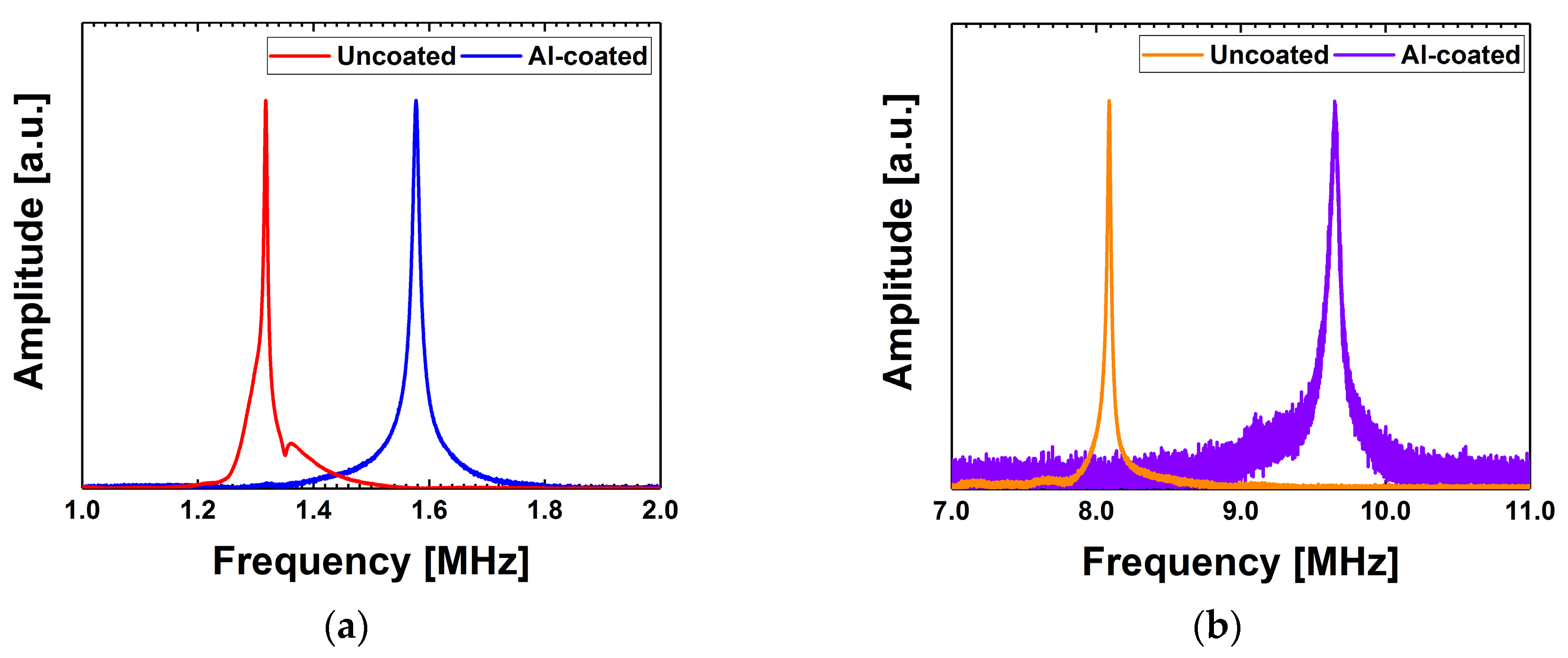
Figure 6 shows the time domain waveforms obtained from the microscale beam testing before and after the film deposition. While the waveforms were measured until 5 ms, they are displayed only up to 0.20 and 0.07 ms for the first- and second-order flexural vibration modes, respectively, after which no significant signals were observed. The fast Fourier transform was performed on the vibration signals and the frequency responses of the microbeams are introduced in Figure 7. Coating of the film resulted in a resonant frequency shift from 1.317 to 1.577 MHz for the first-order vibration mode and from 8.089 to 9.652 MHz for the second-order vibration mode, respectively, indicating an overall increase of the equivalent flexural rigidity of the structure. Results from the finite element analysis are presented in Appendix A, visualizing the microbeam’s deformation behavior.
Resonant frequencies for the first- and second-order vibration modes were computed using the finite element model. During the analysis the Young’s modulus of Al (EAl) was taken as a fitting parameter while other properties, such as the Poisson’s ratio and the density, were kept constant. EAl was adjusted until the resonant frequencies from both the numerical analysis and experiment became identical. EAl = 58 GPa gave good agreement with the measurement data and the results are summarized in Table 2.
It is noted that bulk properties of Au from literature [17] were used in the computation even though it is very thin since the scale effect on Au may not be significant [18,19]. A sensitivity analysis was performed and showed that changes in the Young’s modulus, Poisson’s ratio, and the density of Au by 10% resulted in deviations of EAl by 5.2%, 1.6%, and 11.7%, respectively.
3.3. Picosecond Ultrasonic Measurement
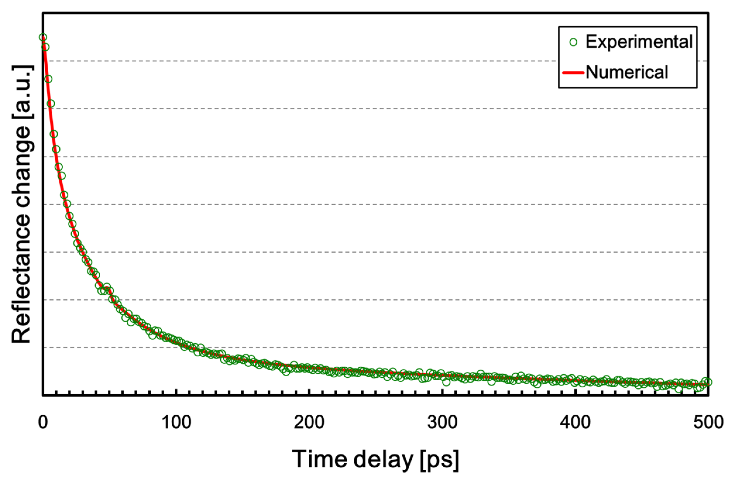
Figure 8 shows the thermoreflectance measurement data using picosecond ultrasonics. Due to the heat conduction in the film, a decrease of reflectivity on the Al surface is observed after t = 0 at which the pump-pulse is applied. In addition, a small peak is observed at t = 48 ps due to the arrival of the longitudinal bulk wave reflected at the Al/Si interface. The solution of the thermoelastically-coupled transient heat conduction equation was computed and curve fitted to the experimental data to estimate the Young’s modulus of the film. During the fitting, only the Young’s modulus was taken as a fitting parameter and evaluated using a trial-and-error approach since the modulus change would shift the peak location of the acoustic response. In addition, the criterion for the best-fit was taken such that the peak location of the acoustic signal from the numerical analysis coincides with that of the experimental data within ±0.5 ps range. Material properties assigned in the numerical analysis are listed in Table 3. Results show that EAl = 60 GPa gives the best-fit, agreeing very well with the microscale beam testing result. Meanwhile, the thermal conductivity and thermal boundary conductance of the Al film were also taken as a fitting parameter, and κAl = 140 W/m·K and σK = 100 MW/m·K were obtained. The thermal conductivity of bulk pure Al is typically 220–240 W/m∙K, but it is often observed to decrease with the reduction of material dimensions [20].
4. Discussion
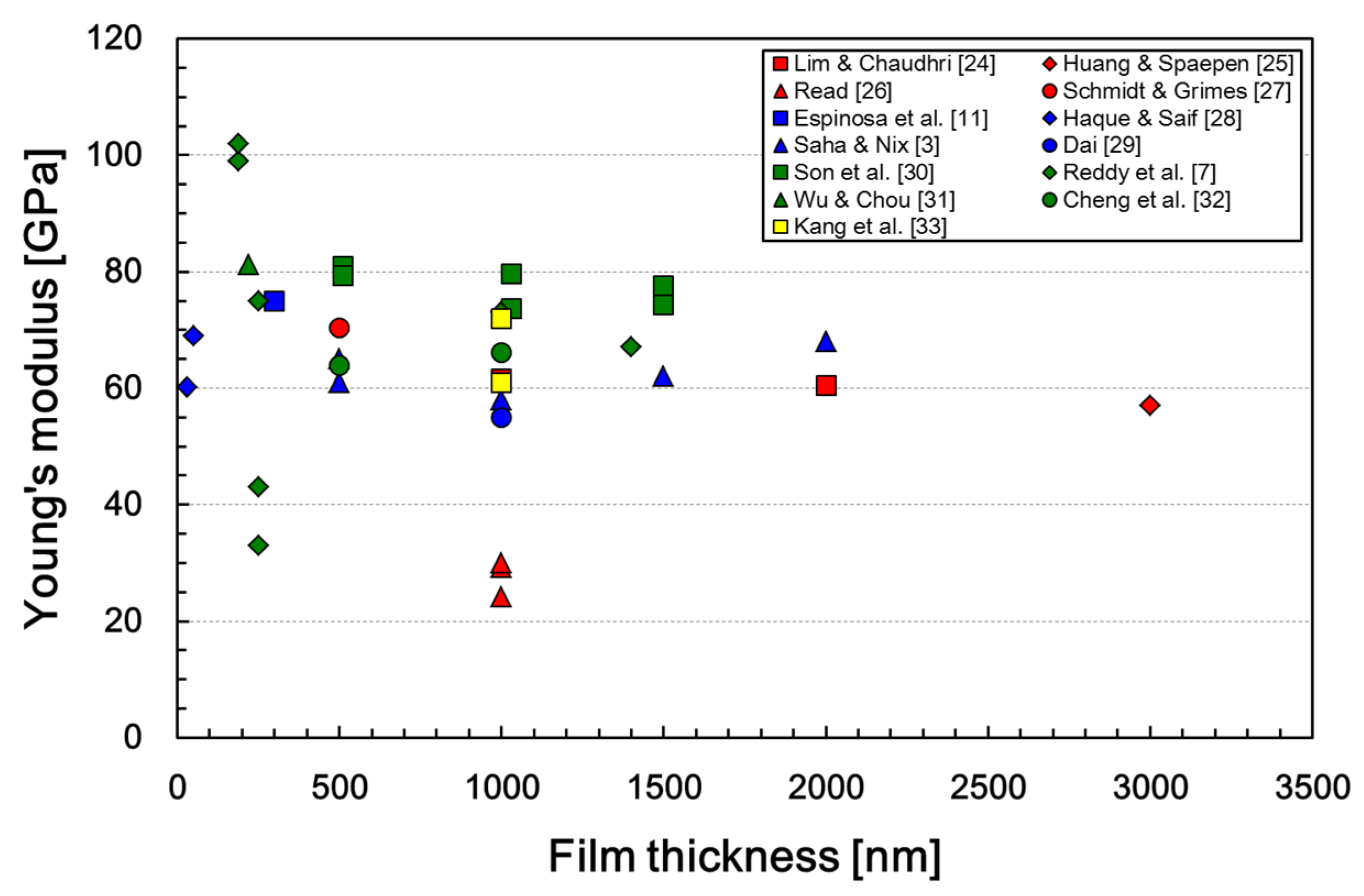
The Young’s modulus of the Al film in the present study is 59 GPa, taking an average of the results from experiments using two different measurement techniques. It should be noted that the anisotropy in the Young’s modulus of Al was not considered in the present study. In certain face-centered cubic metals, such as the copper (Cu) and silver (Ag), the elastic modulus may depend on the crystallographic texture. For example, the stiffness of a Cu thin film was observed to increase as the film thickness decreased due to the increase of <111> fiber texture component [21]. Similarly, the anisotropic elastic-plastic properties of the electrodeposited Ag thin coating were recognized by nanoindentation testing on the longitudinal and transverse directions of the coating surfaces [22]. It was reported, however, that the elastic modulus measured by a cantilever microbeam test was close to that in the parallel direction to the film surface [23]. The bulk property of pure Al is 65–70 GPa in general [24], but the Young’s moduli of Al in the form of a thin-film from literature [3,7,11,24,25,26,27,28,29,30,31,32,33] lie mostly between 55 and 81 GPa, as shown in Figure 9. Outliers are observed such that the results reported by Reddy et al. [7] using a lateral resonator show very large scatter from 33 to 102 GPa. The reason was attributed to geometrical effects from microfabrication issues, such as the scalloping of the beam width during a deep reactive ion etching process. Read et al. [26] also reported an elastic modulus of 24.2–30.0 GPa, which is less than half the bulk property, from tensile tests on free-standing Al specimens. Although it was pointed out that variations in chemical composition, heat treatment, and grain size had little influence on the result, the main reason was not clarified in their study. Therefore, ignoring such deviations, the results in the present study agree well with what were reported in the literature and prove that the proposed techniques are highly effective for thin-film characterization.
5. Conclusions
The Young’s modulus of a nanoscale Al thin-film was evaluated in non-contact and nondestructive ways using two different laser optical measurement techniques. A 153-nm thick Al film was prepared using an e-beam evaporator, and the microbeam testing was performed to detect the natural frequency shift of a cantilever microbeam upon the film deposition. The frequency responses were examined through the fast Fourier transform of time domain waveforms obtained from the laser interferometer, and the mechanical property was calculated through the finite element analysis for the first- and second-order flexural vibration modes. In addition, the picosecond ultrasonics were performed to cross-verify the measurement data. The echo of a longitudinal bulk wave from the Al/Si interface was detected using a femtosecond laser system and the Young’s modulus was obtained through curve fitting of a numerical solution for a transient thermoelastically-coupled equation. The results agree well with each other and show that the average modulus is 59 GPa. A literature survey was also conducted to validate the results and it showed that they fall reasonably well within the range for the Young’s modulus of Al films.
Acknowledgments
This research was supported by the Basic Science Research Program through the National Research Foundation of Korea (NRF) funded by the Ministry of Science & ICT (no. 2015R1C1A1A01053635). The authors thank Jiwon Park and Donggon Kang for assistance in the finite element analysis.
Author Contributions
Yun Young Kim conceived and designed the experiments; Seonwook Lee and Yun Young Kim performed the experiments; Yun Young Kim analyzed the data; Yun Young Kim and Younho Cho contributed reagents/materials/analysis tools; and Seonwook Lee and Yun Young Kim wrote the paper.
Conflicts of Interest
The authors declare no conflict of interest.
Appendix
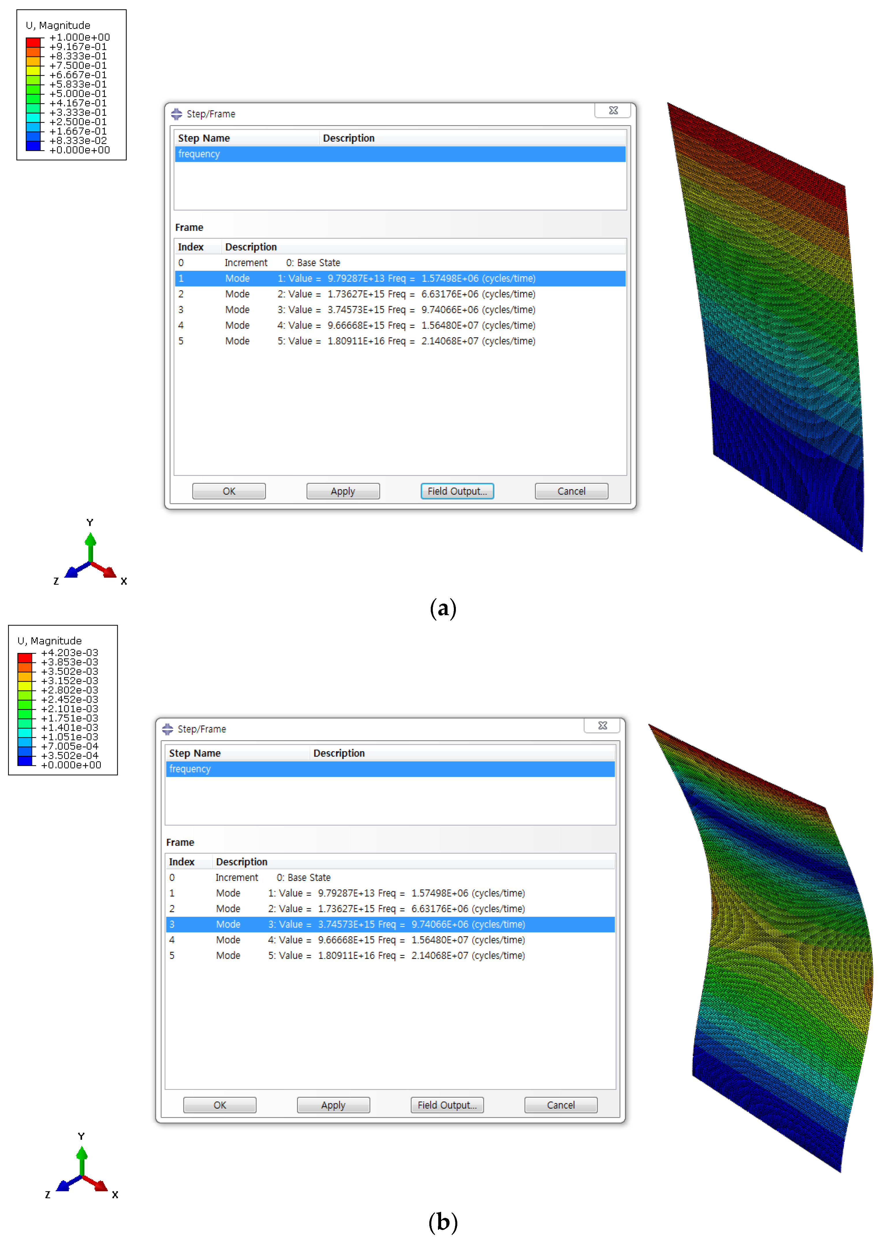
Figure A1 and Figure A2 show the deformation plots from the finite element analysis for the cantilever microbeams in the first- and second-order flexural vibration modes with and without the Al film, respectively. Although not plotted, torsional and lateral vibration modes were also observed.
Figure A1.
Results from the finite element analysis for the cantilever microbeam without the Al film: (a) a deformation plot for the first order flexural vibration mode; and (b) a deformation plot for the second order flexural vibration mode.
Figure A1.
Results from the finite element analysis for the cantilever microbeam without the Al film: (a) a deformation plot for the first order flexural vibration mode; and (b) a deformation plot for the second order flexural vibration mode.
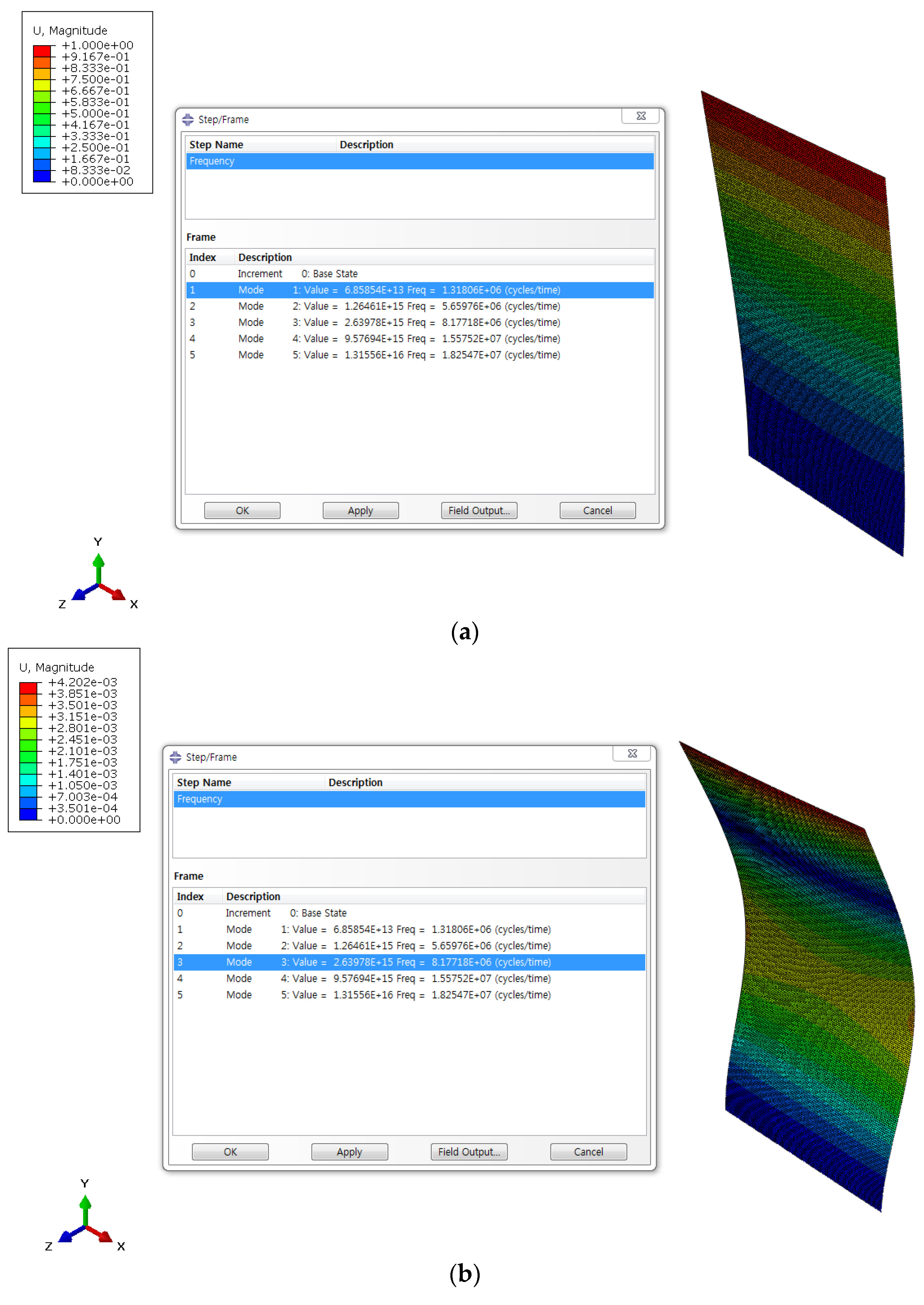
Figure A2.
Results from the finite element analysis for the cantilever microbeam with the Al film: (a) a deformation plot for the first order flexural vibration mode; and (b) a deformation plot for the second order flexural vibration mode.
Figure A2.
Results from the finite element analysis for the cantilever microbeam with the Al film: (a) a deformation plot for the first order flexural vibration mode; and (b) a deformation plot for the second order flexural vibration mode.

References
- Zhang, F.; Krishnaswamy, S.; Lilley, C.M. Bulk-wave and guided-wave photoacoustic evaluation of the mechanical properties of aluminum/silicon nitride double-layer thin films. Ultrasonics 2006, 45, 66–76. [Google Scholar] [CrossRef] [PubMed]
- Kim, Y.Y.; Alwi, H.A.; Awang, R.; Krishnaswamy, S. Influence of radio frequency power on thermal diffusivity of plasma enhanced chemical vapor deposition-grown hydrogenated amorphous carbon thin-films. J. Appl. Phys. 2011, 109, 113503. [Google Scholar]
- Saha, R.; Nix, W.D. Effects of the substrate on the determination of thin film mechanical properties by nanoindentation. Acta Mater. 2002, 50, 23–38. [Google Scholar] [CrossRef]
- Chen, S.; Liu, L.; Wang, T. Investigation of the mechanical properties of thin films by nanoindentation, considering the effects of thickness and different coating–substrate combinations. Surf. Coat. Technol. 2005, 191, 25–32. [Google Scholar] [CrossRef]
- Zhao, D.; Qian, X.; Gu, X.; Jajja, S.A.; Yang, R. Measurement techniques for thermal conductivity and interfacial thermal conductance of bulk and thin film materials. J. Electron. Packag. 2016, 138, 040802. [Google Scholar] [CrossRef]
- Chaudhary, M.; Gupta, A. Microcantilever-based sensors. Def. Sci. J. 2009, 59, 634–641. [Google Scholar] [CrossRef]
- Reddy, A.; Kahn, H.; Heuer, A.H. A mems-based evaluation of the mechanical properties of metallic thin films. J. Microelectromech. Syst. 2007, 16, 650–658. [Google Scholar] [CrossRef]
- Strandjord, A.J.; Popelar, S.; Jauernig, C. Interconnecting to aluminum-and copper-based semiconductors (electroless-nickel/gold for solder bumping and wire bonding). Microelectron. Reliab. 2002, 42, 265–283. [Google Scholar] [CrossRef]
- Hamon, Y.; Brousse, T.; Jousse, F.; Topart, P.; Buvat, P.; Schleich, D. Aluminum negative electrode in lithium ion batteries. J. Power Sour. 2001, 97, 185–187. [Google Scholar] [CrossRef]
- Shaheen, S.E.; Radspinner, R.; Peyghambarian, N.; Jabbour, G.E. Fabrication of bulk heterojunction plastic solar cells by screen printing. Appl. Phys. Lett. 2001, 79, 2996–2998. [Google Scholar] [CrossRef]
- Espinosa, H.; Zhu, Y.; Fischer, M.; Hutchinson, J. An experimental/computational approach to identify moduli and residual stress in mems radio-frequency switches. Exp. Mech. 2003, 43, 309–316. [Google Scholar] [CrossRef]
- Stephanou, P.; Pisano, A. PS-4 GHZ contour extensional mode aluminum nitride MEMS resonators. In Proceedings of the 2006 IEEE Ultrasonics Symposium, Vancouver, BC, Canada, 3–6 October 2006; pp. 2401–2404. [Google Scholar]
- Kim, Y.Y. An advanced characterization method for the elastic modulus of nanoscale thin-films using a high-frequency micromechanical resonator. Materials 2017, 10, 806. [Google Scholar] [CrossRef] [PubMed]
- Richardson, C.; Ehrlich, M.; Wagner, J. Interferometric detection of ultrafast thermoelastic transients in thin films: Theory with supporting experiment. J. Opt. Soc. Am. B Opt. Phys. 1999, 16, 1007–1015. [Google Scholar] [CrossRef]
- Stevens, R.J.; Smith, A.N.; Norris, P.M. Measurement of thermal boundary conductance of a series of metal-dielectric interfaces by the transient thermoreflectance technique. J. Heat Transfer 2005, 127, 315–322. [Google Scholar] [CrossRef]
- Miklós, A.; Bozóki, Z.; Lörincz, A. Picosecond transient reflectance of thin metal films. J. Appl. Phys. 1989, 66, 2968–2972. [Google Scholar] [CrossRef]
- Shackelford, J.F.; Han, Y.-H.; Kim, S.; Kwon, S.-H. CRC Materials Science and Engineering Handbook; CRC Press: Boca Raton, FL, USA, 2016. [Google Scholar]
- Huh, Y.-H.; Kim, D.-I.; Kim, D.-J.; Lee, H.-M.; Park, J.-H. Dependency of micro-mechanical properties of gold thin films on grain size. In Engineering against Fracture; Springer: Berlin, Germany, 2009; pp. 339–346. [Google Scholar]
- Pamula, V.K.; Jog, A.; Fair, R.B. Mechanical property measurement of thin-film gold using thermally actuated bimetallic cantilever beams. In Proceedings of the Fourth International Conference on Modeling and Simulation of Microsystems, Hilton Head, SC, USA, 19–21 March 2001. [Google Scholar]
- Stojanovic, N.; Yun, J.; Washington, E.B.; Berg, J.M.; Holtz, M.W.; Temkin, H. Thin-film thermal conductivity measurement using microelectrothermal test structures and finite-element-model-based data analysis. J. Microelectromech. Syst. 2007, 16, 1269–1275. [Google Scholar] [CrossRef]
- Xiang, Y.; Tsui, T.; Vlassak, J.J. The mechanical properties of freestanding electroplated Cu thin films. J. Mater. Res. 2006, 21, 1607–1618. [Google Scholar] [CrossRef]
- Cheng, G.; Sun, X.; Wang, Y.; Tay, S.L.; Gao, W. Nanoindentation study of electrodeposited ag thin coating: An inverse calculation of anisotropic elastic-plastic properties. Surf. Coat. Technol. 2017, 310, 43–50. [Google Scholar] [CrossRef]
- Hong, S.; Kim, K.; Kim, Y.-M.; Hahn, J.-H.; Lee, C.-S.; Park, J.-H. Characterization of elastic moduli of Cu thin films using nanoindentation technique. Compos. Sci. Technol. 2005, 65, 1401–1408. [Google Scholar] [CrossRef]
- Lim, Y.; Chaudhri, M.; Enomoto, Y. Accurate determination of the mechanical properties of thin aluminum films deposited on sapphire flats using nanoindentations. J. Mater. Res. 1999, 14, 2314–2327. [Google Scholar] [CrossRef]
- Huang, H.; Spaepen, F. Tensile testing of free-standing Cu, Ag and Al thin films and Ag/Cu multilayers. Acta Mater. 2000, 48, 3261–3269. [Google Scholar] [CrossRef]
- Read, D.T.; Cheng, Y.-W.; Keller, R.R.; McColskey, J.D. Tensile properties of free-standing Aluminum thin films. Scr. Mater. 2001, 45, 583–589. [Google Scholar] [CrossRef]
- Schmidt, S.; Grimes, C.A. Characterization of nano-dimensional thin-film elastic moduli using magnetoelastic sensors. Sens. Actuators A Phys. 2001, 94, 189–196. [Google Scholar] [CrossRef]
- Haque, M.; Saif, M.A. Mechanical behavior of 30–50 nm thick Aluminum films under uniaxial tension. Scr. Mater. 2002, 47, 863–867. [Google Scholar] [CrossRef]
- Dai, C.-L. In situ electrostatic microactuators for measuring the Young’s modulus of CMOS thin films. J. Micromech. Microeng. 2003, 13, 563. [Google Scholar] [CrossRef]
- Son, D.; Jeong, J.-H.; Kwon, D. Film-thickness considerations in microcantilever-beam test in measuring mechanical properties of metal thin film. Thin Solid Films 2003, 437, 182–187. [Google Scholar] [CrossRef]
- Wu, L.-C.; Chou, Y.-F. On-wafer characterization of thermomechanical properties of isotropic thin films deposited on anisotropic substrates. Jpn. J. Appl. Phys. 2008, 47, 5623. [Google Scholar] [CrossRef]
- Cheng, Y.-C.; Tong, C.-J.; Lin, M.-T. Measurement of static and dynamic mechanical behavior of micro and nano-scale thin metal films: Using micro-cantilever beam deflection. Microsyst. Technol. 2011, 17, 721–730. [Google Scholar] [CrossRef]
- Kang, T.J.; Kim, J.-G.; Lee, H.-Y.; Lee, J.-S.; Lee, J.-H.; Hahn, J.-H.; Kim, Y.H. Modification of optical and mechanical surface properties of sputter-deposited aluminum thin films through ion implantation. Int. J. Precis. Eng. Manuf. 2014, 15, 889–894. [Google Scholar] [CrossRef]
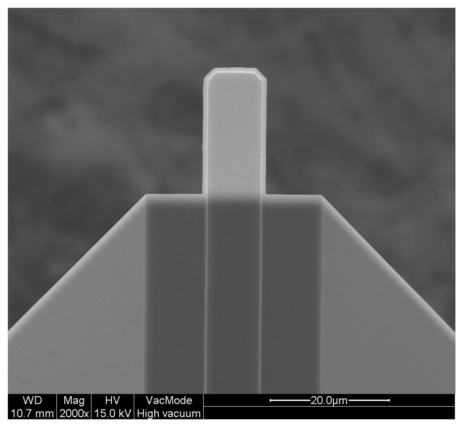
Figure 1.
Field emission scanning electron microscopy image of the cantilever microbeam.

Figure 2.
Film thickness measurement data.
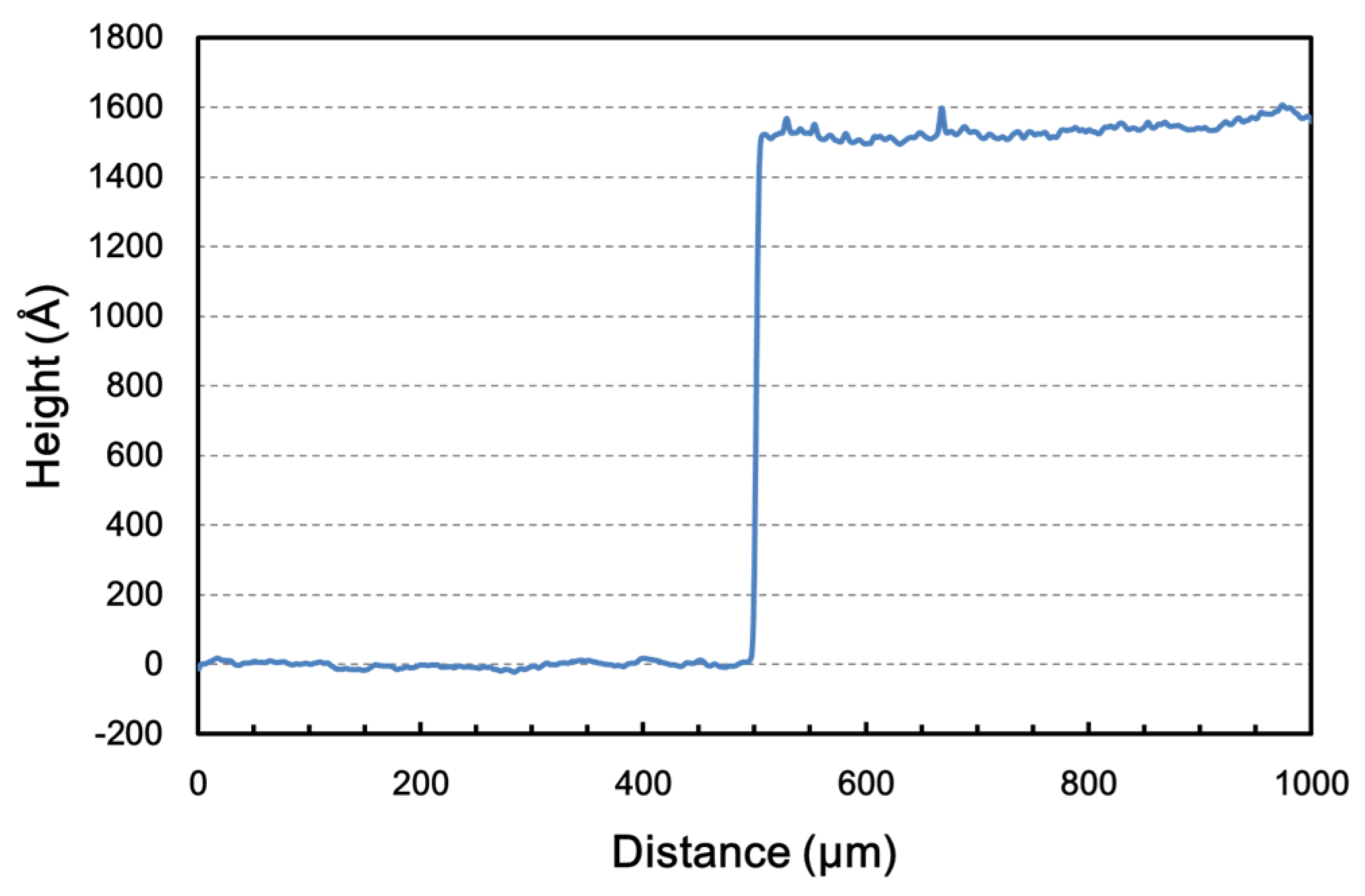
Figure 3.
(a) A meshed geometry for the finite element analysis; (b) a ply stack plot of the cantilever microbeam without the Al film; and (c) a ply stack plot of the Al-coated microbeam.
Figure 3.
(a) A meshed geometry for the finite element analysis; (b) a ply stack plot of the cantilever microbeam without the Al film; and (c) a ply stack plot of the Al-coated microbeam.
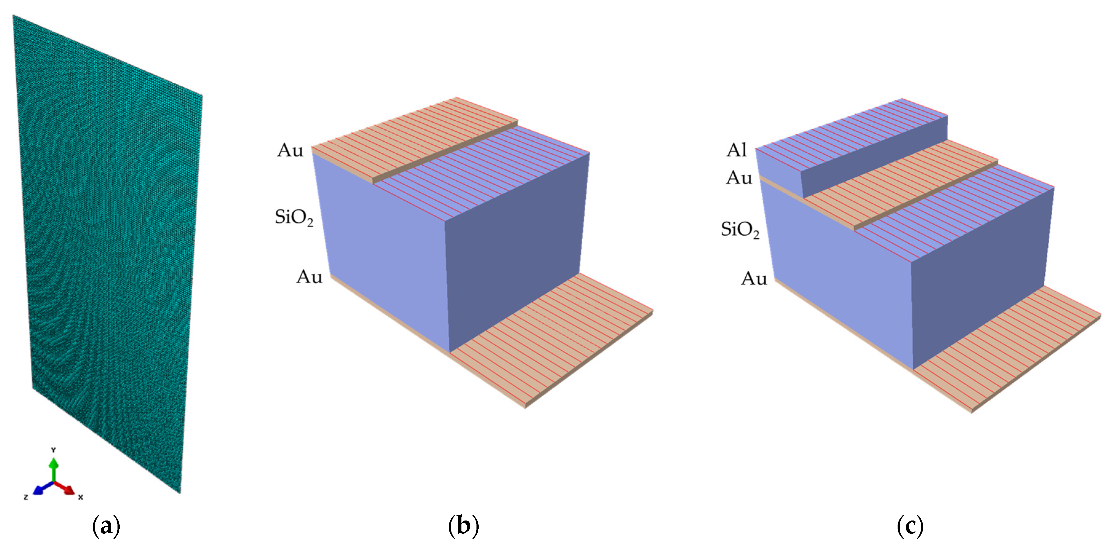
Figure 4.
A plot of the grid independence test result.
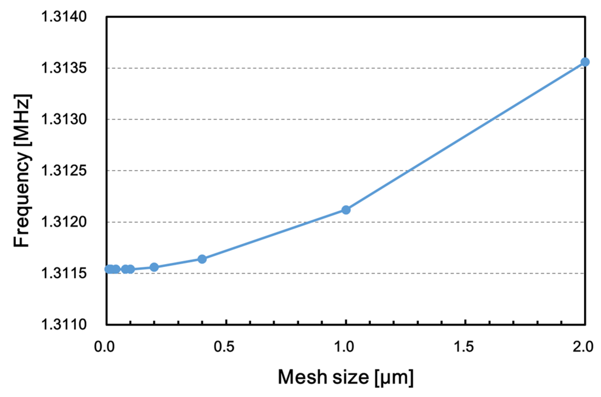
Figure 5.
(a) An atomic force microscopy image of the aluminum thin film surface and (b) the grazing incidence X-ray diffraction measurement data.
Figure 5.
(a) An atomic force microscopy image of the aluminum thin film surface and (b) the grazing incidence X-ray diffraction measurement data.
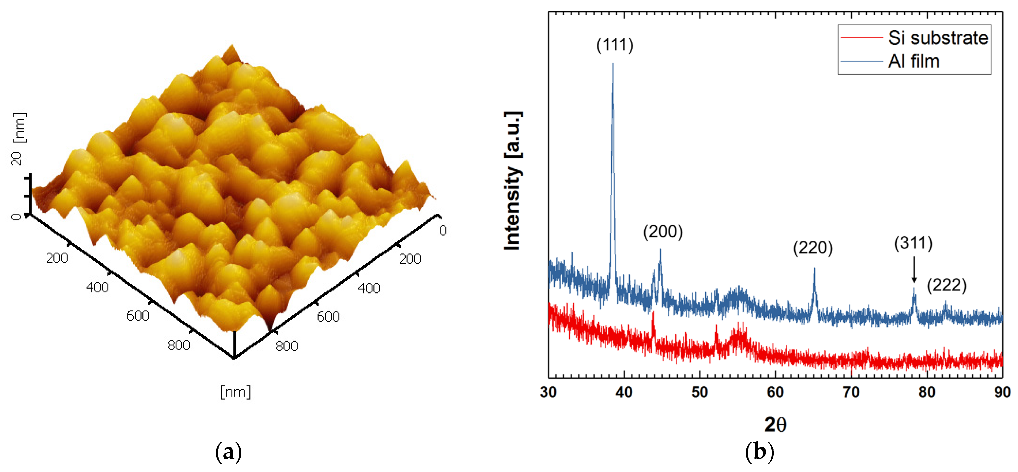
Figure 6.
Time domain waveforms of the resonating cantilever microbeam before and after the Al coating: (a) vibration signals in the first-order flexural mode; and (b) vibration signals in the second-order flexural mode.
Figure 6.
Time domain waveforms of the resonating cantilever microbeam before and after the Al coating: (a) vibration signals in the first-order flexural mode; and (b) vibration signals in the second-order flexural mode.
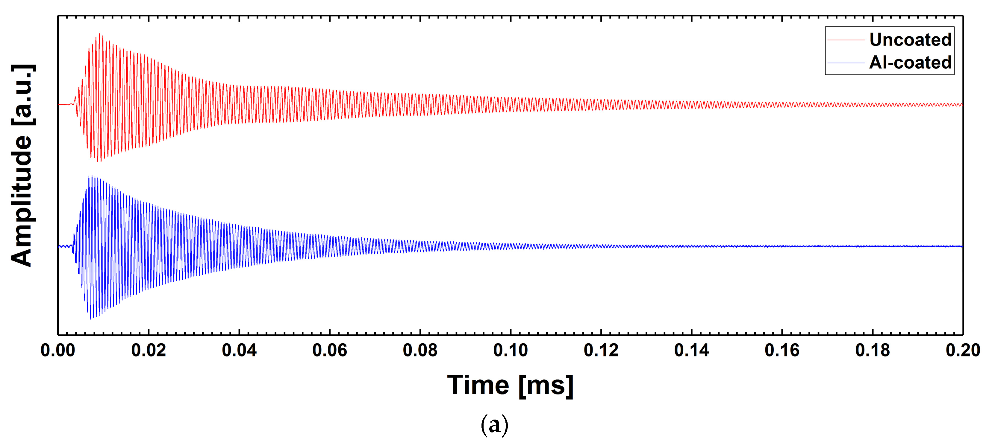
Figure 7.
Fast Fourier transform results of the time domain waveforms: (a) frequency responses in the first-order flexural mode; and (b) frequency responses in the second-order flexural mode.
Figure 7.
Fast Fourier transform results of the time domain waveforms: (a) frequency responses in the first-order flexural mode; and (b) frequency responses in the second-order flexural mode.

Figure 8.
A plot of the reflectance change on the Al film surface.

Table 1.
Material properties used in the finite element analysis.
| Property | Material | ||
|---|---|---|---|
| SiO2 | Au | Al | |
| Young’s modulus (GPa) | 72.0 | 79.0 | – |
| Poisson’s ratio | 0.17 | 0.44 | 0.35 |
| Density (kg/m3) | 2200 | 19,300 | 2700 |
Table 2.
Resonant frequencies obtained from the experiment and the finite element analysis.
| Method | Sample | Resonant Frequency | |
|---|---|---|---|
| 1st Order | 2nd Order | ||
| Experiment | Uncoated | 1.317 | 8.089 |
| Al-coated | 1.577 | 9.652 | |
| Finite element analysis | Uncoated | 1.318 | 8.177 |
| Al-coated 1 | 1.575 | 9.741 | |
1 EAl = 58 GPa was used.
Table 3.
Material properties used in the longitudinal bulk wave propagation simulation.
| Property | Material | |
|---|---|---|
| Al | Si | |
| Density (kg/m3) | 2700 | 2330 |
| Specific heat (J/kg·K) | 900 | 700 |
| Thermal conductivity (W/m·K) | 140 | 148 |
| Coefficient of thermal expansion (μ/K) | 24.0 | 2.6 |
| Young’s modulus (GPa) | – | 130 |
| Poisson’s ratio | 0.35 | 0.25 |
| Refractive index | 2.23 | – |
| Extinction coefficient | 7.60 | – |
| Surface reflectivity | 0.88 | – |
© 2017 by the authors. Licensee MDPI, Basel, Switzerland. This article is an open access article distributed under the terms and conditions of the Creative Commons Attribution (CC BY) license (http://creativecommons.org/licenses/by/4.0/).
Share and Cite
MDPI and ACS Style
Lee, S.; Kim, Y.Y.; Cho, Y. A Comparative Study on the Elastic Characteristics of an Aluminum Thin-Film Using Laser Optical Measurement Techniques. Coatings 2017, 7, 143. https://doi.org/10.3390/coatings7090143
AMA Style
Lee S, Kim YY, Cho Y. A Comparative Study on the Elastic Characteristics of an Aluminum Thin-Film Using Laser Optical Measurement Techniques. Coatings. 2017; 7(9):143. https://doi.org/10.3390/coatings7090143
Chicago/Turabian StyleLee, Seonwook, Yun Young Kim, and Younho Cho. 2017. "A Comparative Study on the Elastic Characteristics of an Aluminum Thin-Film Using Laser Optical Measurement Techniques" Coatings 7, no. 9: 143. https://doi.org/10.3390/coatings7090143
Note that from the first issue of 2016, this journal uses article numbers instead of page numbers. See further details here.