Tunnel Oxides Formed by Field-Induced Anodisation for Passivated Contacts of Silicon Solar Cells

1
School of Photovoltaic and Renewable Energy Engineering, UNSW, Sydney, NSW 2052, Australia
2
Mark Wainwright Analytical Centre, UNSW, Sydney, NSW 2052, Australia
*
Author to whom correspondence should be addressed.
Coatings 2018, 8(2), 81; https://doi.org/10.3390/coatings8020081
Submission received: 5 January 2018
/
Revised: 15 February 2018
/
Accepted: 19 February 2018
/
Published: 23 February 2018
(This article belongs to the Special Issue Advanced Surface Passivation Processes for Solar Cells)
Abstract
:Tunnel silicon oxides form a critical component for passivated contacts for silicon solar cells. They need to be sufficiently thin to allow carriers to tunnel through and to be uniform both in thickness and stoichiometry across the silicon wafer surface, to ensure uniform and low recombination velocities if high conversion efficiencies are to be achieved. This paper reports on the formation of ultra-thin silicon oxide layers by field-induced anodisation (FIA), a process that ensures uniform oxide thickness by passing the anodisation current perpendicularly through the wafer to the silicon surface that is anodised. Spectroscopical analyses show that the FIA oxides contain a lower fraction of Si-rich sub-oxides compared to wet-chemical oxides, resulting in lower recombination velocities at the silicon and oxide interface. This property along with its low temperature formation highlights the potential for FIA to be used to form low-cost tunnel oxide layers for passivated contacts of silicon solar cells.
1. Introduction
Ultra-thin and uniform silicon oxide (SiOx) layers have played a key role as an interfacial layer in a number of high efficiency silicon solar cell designs, including acting as intermediate layers in metal-insulator-semiconductor (MIS) solar cells [1], enhancing passivation at amorphous/crystalline silicon (a-Si:H/c-Si) heterojunction interfaces [2,3,4] and passivating thin metal-oxide passivated contacts [5,6] and poly-silicon (poly-Si) contacts [7,8,9,10,11,12,13,14]. For full-area poly-Si contacts, the insertion of the SiOx layer between poly-Si and c-Si substrate provides effective interface passivation and allows one dimensional carrier flow through the solar cell [8]. These attributes have enabled energy conversion efficiencies exceeding 25% to be achieved [7,8,15,16]. Previous studies have shown that the quality of the tunnel oxide is of great importance to the cell performance [15]. To ensure high open-circuit voltages (Voc) and fill factors (FF), the SiOx layer needs to be homogeneous and as stoichiometric as possible to provide excellent passivation to the c-Si substrate and simultaneously to be sufficiently thin to ensure a low contact resistivity [9]. Moreover, the interface charge density of the tunnel layer has been reported to contribute to the effectiveness of field-effect passivation on silicon surfaces if a high positively-charged tunnel layer is adopted for electron-extracting contacts and high negatively-charged tunnel layer is used for hole-extracting contacts [17].
Oxidation techniques used to form ultra-thin SiOx layers for poly-Si contacts include thermal oxidation [18,19,20], wet-chemical oxidation by HNO3 [7,21,22] and ozone oxidation [15]. The former method requires critical wafer cleaning and a high thermal budget, which is not typically compatible with reducing manufacturing costs in the photovoltaic industry. Although the latter two techniques can potentially reduce process costs, the SiOx layers grown by HNO3 oxidation contain a high fraction of sub-oxides which are not ideal for interface passivation [15] and the ozone oxidation allows limited control over oxide properties. Consequently, the development of a room temperature oxidation process that is more compatible with current cell production lines is desirable.
Grant et al. [23,24] reported room temperature anodisation of silicon in HNO3 with the obtained oxide having a surface recombination velocity comparable to that of thermally-grown oxide after a low temperature anneal. However, the reported method was based on a traditional clipping arrangement where the applied bias generates a potential gradient laterally across the wafer, resulting in non-uniform oxidation. To address this issue, processes have been developed that use illumination or an electric field to induce a current flowing through the wafer in a direction that is perpendicular to the surface that is anodised [25,26,27]. These methods, which are called light-induced anodisation (LIA) and field-induced anodisation (FIA) respectively, offer the potential to uniformly anodise industrial-sized solar cells using a lower current than would be required by the clipping method.
In this paper, we extend the brief report on the formation of thin SiOx layers on n-type silicon (n-Si) surfaces using FIA [28] with a more systematic study on the oxide stoichiometry and resulting passivation quality. The performance of the SiOx layers is then compared to that of the wet-chemically grown oxides and thermally-grown oxides.
Overview of the FIA Process
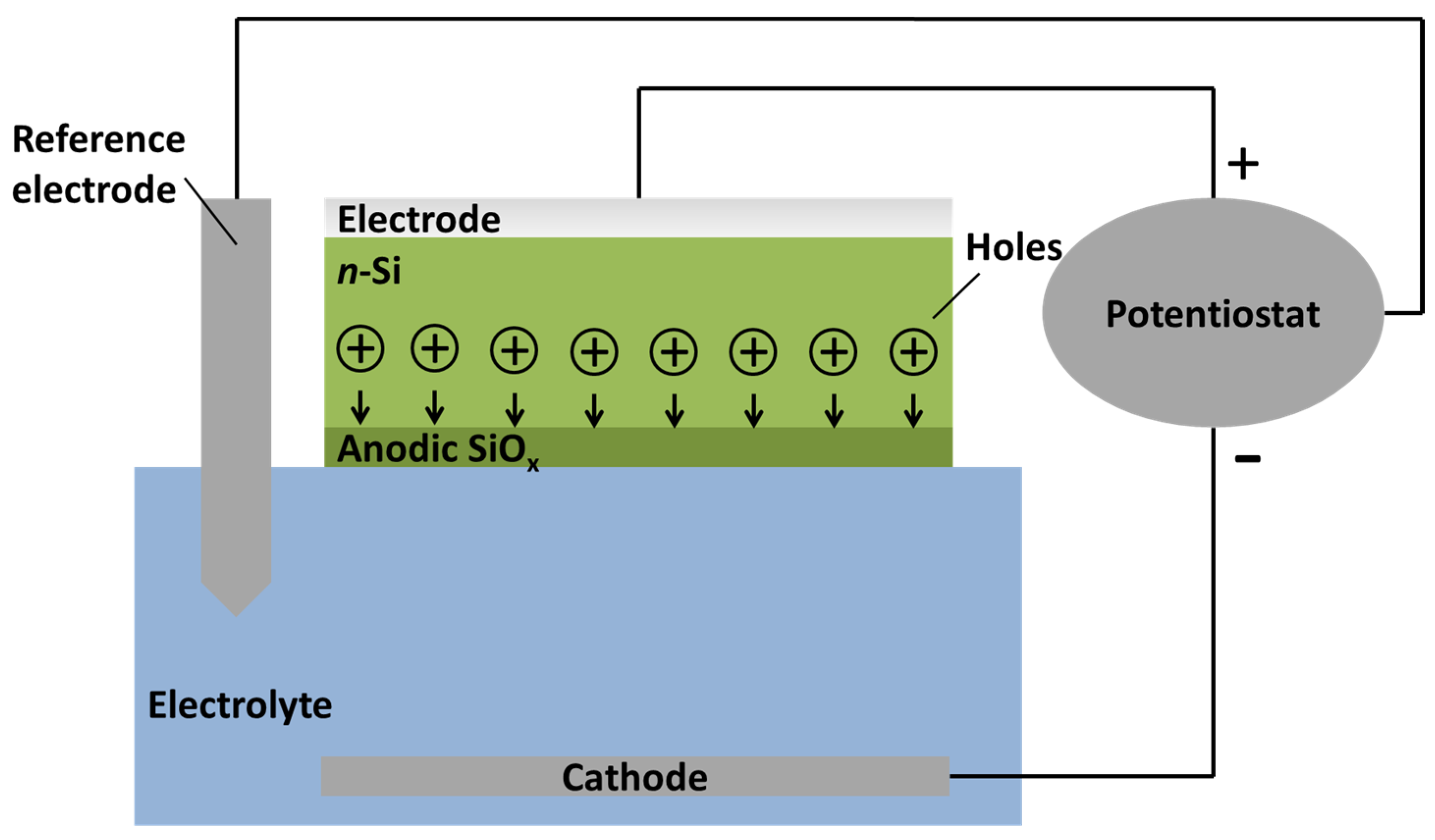
Light-induced anodization can be used to oxidise p-type silicon (p-Si) surfaces of a solar cell [27,29]. SiOx layers of uniform thickness can be grown by placing the p-Si surface in contact with the electrolyte and using an external power source bias applied to the n-Si surface of the solar cell to offset resistive losses in the electrochemical circuit and enable the p-Si surface to be oxidised by the light-induced current of the solar cell. When oxidising n-Si surfaces of a solar cell, the FIA process can be employed with n-Si surfaces contacting the electrolyte and a positive bias voltage or current applied to the p-Si to forward bias the junction so that current can flow through the wafer to oxidise the n-Si surfaces.
It should be noted that when forward biasing a p-n junction in the FIA process, if the surfaces are not sufficiently doped, Schottky diodes can form with the depletion region extending further into the wafer with increasing anodisation bias and rectifying current flow through the wafer [30]. This can be addressed through the use of illumination to generate a photocurrent across the depletion regions at the silicon surfaces so that generated carriers can be swept out of the regions by the applied electric field, allowing current to flow through the wafer. The FIA process can also be used to grow silicon oxides on devices without p-n junctions. Figure 1 shows a schematic diagram of the FIA setup that can be used to anodise an n-Si wafer surface. The wafer is made anodic by applying a positive bias via a semi-transparent aluminum contact electrode which is applied uniformly over the wafer surface enabling the entire surface to be anodised. Even though the oxide may start to grow non-uniformly across the wafer surface, the anodization current continues to flow through less resistive paths until the resistance provided by the anodic oxide reaches the same through the entire wafer surface, securing a uniform final oxide thickness. The thickness of the oxide can be controlled by anodisation voltage/current, electrolyte constitution/concentration, and light intensity, suggesting FIA may be a promising alternative when forming a uniform and controllable tunneling SiOx at room temperature.
2. Experimental
The samples used for the thickness and compositional study were phosphorus-doped (n-type) double-side polished Czochralski (Cz) (100) silicon wafers (4 cm × 4 cm) with a thickness of 525 µm and a resistivity of 0.8 Ω·cm. The wafers were cleaned via a standard wafer cleaning sequence developed by the Radio Corporation of America (RCA) [31] followed by immersion in 1% (w/v) hydrofluoric acid (HF) for 2 min prior to the anodisation process. The wafers were then anodised in 0.5 M H2SO4 with the voltage being sensed by a reference electrode. Considering the electrolyte may induce band bending at the silicon surface, an illumination was used to ensure photo-current flow across depletion regions that can form at the electrolyte interface [30].
The thickness of the oxide was evaluated using an ellipsometer from J.A Woollam Co., Inc., Lincoln, NE, USA, (M-2000VI) with a refractive index of 1.46 [32]. Five independent measurements were performed across the surface of the wafers to assess the uniformity of the oxide growth. The FIA SiOx sample used for thickness and uniformity check for scanning transmission electron microscopy (STEM) and energy dispersive X-ray spectroscopy (EDS) analyses were anodised using a pulsed voltage source with 50% positive cycle at 1 V and 50% negative cycle at −1 V for the duration of 20 min under an illumination of 100 W/m2. For the following X-ray photoelectron spectroscopy (XPS) analysis and surface passivation assessment, the FIA SiOx layers were grown using a constant voltage of 1 V for 20 min with an illumination of 100 W/m2. The thickness and elemental composition of the ultra-thin anodic SiOx layers were measured using a JOEL JEM-ARM200F (200kV) aberration-corrected STEM equipped with an EDS system. The STEM sample was prepared by making a lamella from a dual-beam focused ion beam (FIB) system. The XPS from Thermo Scientific UK (ESCALAB250Xi) under ultra-high vacuum (> 2 × 10⁻⁹ mbar) was used to characterize the stoichiometry of the FIA oxide. The X-ray source was monochromated Al Kα (hυ × 1486.68 eV) with the binding energy scale calibrated using a carbon reference (C 1s = 284.8 eV). Photo electrons were collected in the surface-normal direction. The oxide grown by immersion (without an applied bias) in 0.5 M H2SO4 for 20 min under an illumination of 100 W/m2 was also analysed by XPS as a reference. In addition, the stoichiometry of the tunnel oxide of a comparable thickness formed by thermal oxidation (in a SEMCO reduced pressure oxidation furnace at 600 °C for 20 min) and wet-chemical oxidation (in 68 wt % HNO3 acid at 121 °C for 10 min) was also studied for comparison purposes. In order to minimize the ultra-thin oxide from being contaminated by air and/or moisture, oxide samples were kept in a nitrogen environment during transportation for the XPS measurements.
N-type (100) double-side polished Cz-Si wafers with a resistivity of 10–12 Ω·cm and a thickness of ~525 μm were used for the effective minority carrier lifetime (τeff) measurements. The wafers were cleaned using the same procedure described above followed by an HF dip before the growth of the ultra-thin SiOx layer by FIA, thermal oxidation and HNO3 oxidation on both sides of the wafers. Note that the same circuit was used when growing FIA SiOx on both sides of the wafers. The wafers were rinsed and dried after the first surface was anodised, then turned over to enable the other surface to be in contact with the electrolyte. When anodising the second surface, the semi-transparent aluminum electrode was placed on top of the anodised surface so that current could tunnel through the ultra-thin SiOx layer before entering the silicon and allowing the second surface to be anodised. Passivation of the ultra-thin SiOx layers was assessed together with a capping layer of ~100 nm amorphous silicon nitride (referred to as SiNx in the following). A dual-mode (MW/RF) laboratory scale PECVD system from Roth & Rau (AK400, Hohenstein-Ernstthal, Germany) was used for the SiNx deposition. A forming gas anneal (FGA) at 400 °C for 10 min was performed on all lifetime samples after SiNx deposition. The 𝜏eff was measured under transient mode using a Sinton WCT-120 bridge from Sinton Instruments after SiNx deposition and after FGA. Symmetrical lifetime samples were used to evaluate the passivation quality of the SiOx/SiNx stacks, allowing the upper limit surface recombination velocity (Seff_UL) to be extracted from the following equation:
where W is the Si substrate thickness and τbulk_intrinsic is the Si intrinsic bulk lifetime as parameterized by Richter et al. [33].
3. Results and Discussion
3.1. Ellipsometry Measurements of Oxide Thickness
Figure 2 graphs the thickness of the SiOx layer formed by FIA as a function of time. The oxide thickness grown by immersion is compared to the growth profile generated from three different bias voltages with and without illumination. As can be seen, when growing FIA oxide in dark, the thickness over time profile is similar to that of the oxide formed by immersion in the same electrolyte without applying a bias voltage. An illumination of the n-Si surfaces with a relatively low intensity of 2 W/cm2 was able to almost double the growth rate of the oxide when anodising at 1.5 V for less than 8 min. This demonstrates that an illumination is required to secure current flow through depletion regions that can form at the electrolyte interface as a result of the band bending induced by the electrolyte. It is proposed that when forming thin anodic oxides using FIA, the oxide growth is predominately controlled by the supply of positive charge at the electrolyte interface, whereas, for thicker oxides, the diffusion ofoxidant from the acidic electrolyte through the formed oxide layer to the silicon-oxide interface would dominate the oxide growth. As this study concentrates on the formation of ultra-thin tunneling oxide layers, the thickness of the oxide is primarily governed by the applied potential. When the applied voltage was increased from 1.5 V to 3.0 V, the oxide thickness increased from 2.34 ± 0.03 to 3.37 ± 0.07 nm. It was also found that the uniformity of the oxide across the wafer was improved with longer anodisation times as observed with narrower error bars, which is consistent with the oxide growing until the resistance was the same across the entire exposed silicon area.
3.2. Microscopic and Spectroscopic Analyses
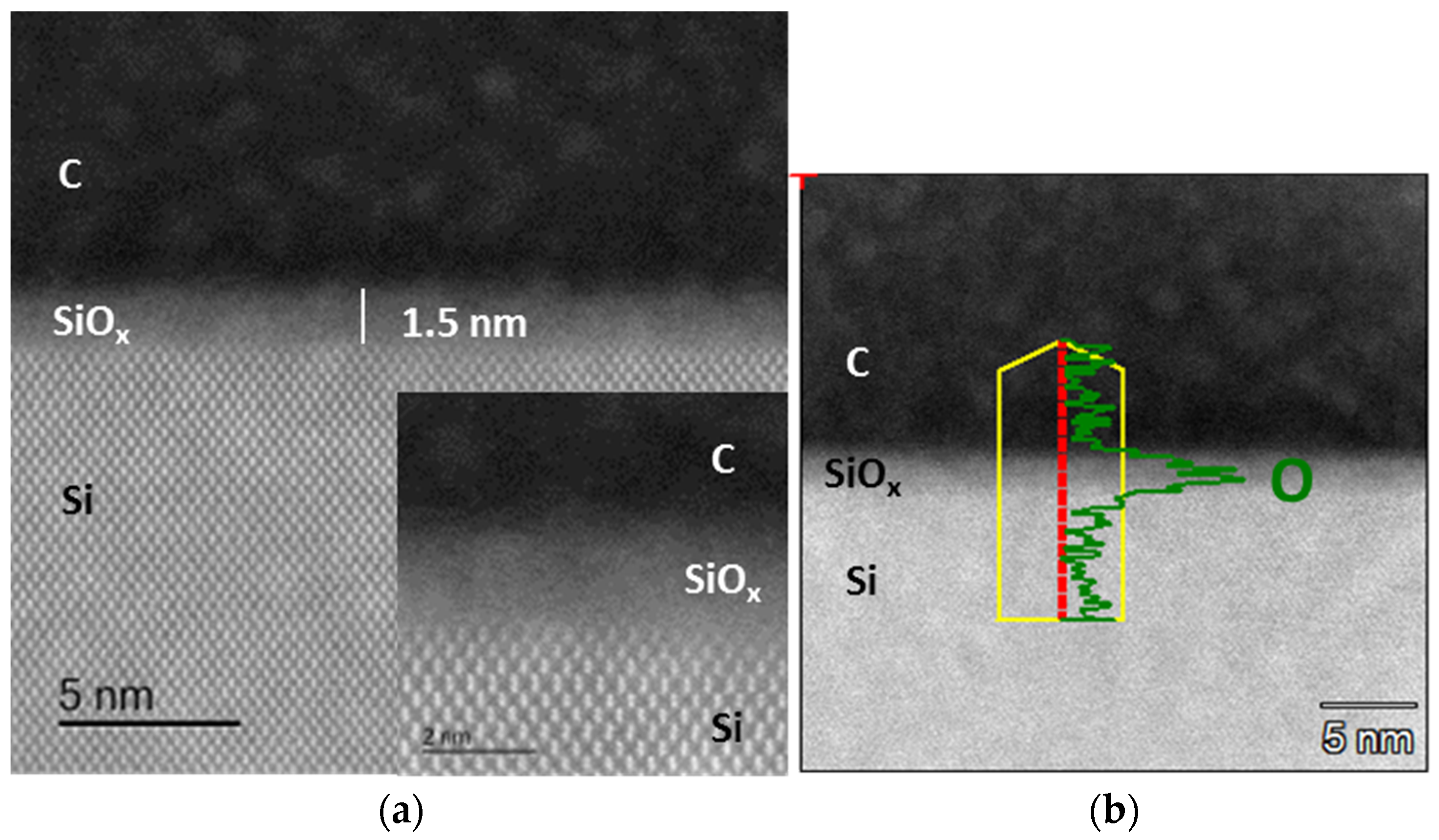
The thickness and uniformity of the anodic oxide layer were also assessed using high-resolution transmission electron microscopy (HRTEM). Figure 3 shows the cross-sectional images of the SiOx layer grown by FIA using a pulsed voltage (varying between 1 V and −1 V) for 20 min under an illumination of 100 W/m2. A capping layer of carbon (C) was deposited for preparation and protection purposes. Oxide thickness was measured at several points across the sample with an average thickness determined to be 1.5 nm, which is lower than the thickness (2.0 nm) measured and fitted from ellipsometry using a refractive index of thermal oxide (i.e., ~1.46). This suggests the refractive index of the anodic oxides may be higher than that of thermally-grown oxide, at least for the oxides grown using longer anodisation time. This could be due to a denser anodic oxide being formed at the silicon interface as revealed by previous reports that the first 1–2 nm anodic oxide has a density of 2.5 g/cm3 which is higher than value of 2.2 g/cm3 for stoichiometric SiO2 [34]. The larger density can be attributed to the existence of a layer with accumulated mechanical stress at the anodic oxide and silicon interface [34]. The different SiOx layer thickness estimated from ellipsometry measurements and the TEM images could be due to the presence of a transition region containing mostly silicon sub-oxides at the silicon surface which is difficult to differentiate from the SiO2 in TEM images and contributes to possible errors in estimating the oxide thickness using ellipsometry data. Models chosen to fit ellipsometry data can include additional detail such as an intermixing layer at the silicon and SiOx interface which can directly impact the accuracy of the determined SiOx thickness, however in this work the SiOx layer was modelled as a single layer with a refractive index value of 1.46. The accuracy of the thickness estimate from the TEM images may have been impacted by adsorption of moisture at the surface before capping.
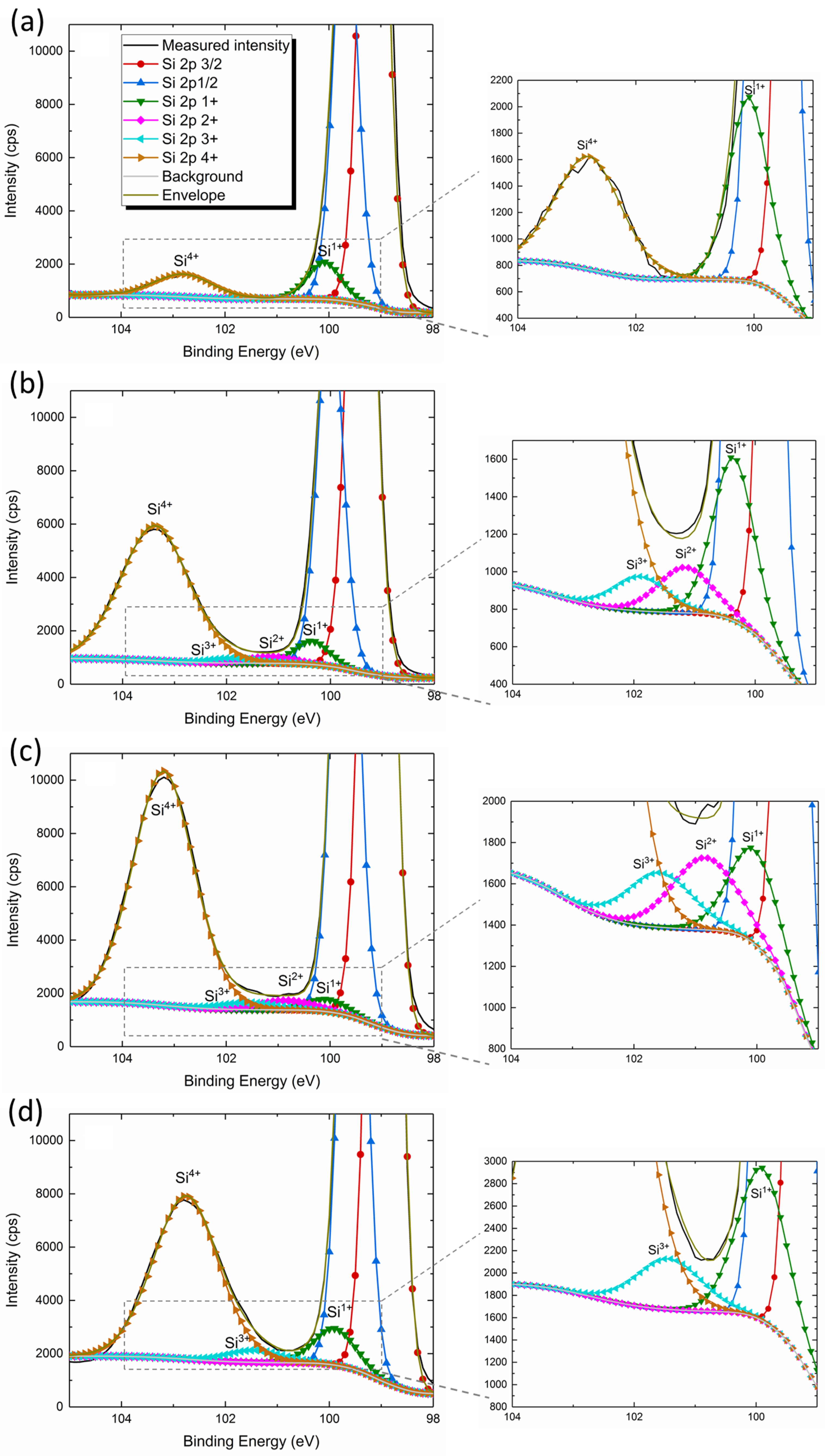
X-ray photon spectroscopy was used to obtain information on the elemental composition of the anodised oxide films. When growing ultra-thin SiOx with low applied bias voltages during the FIA process, the oxide resulting from immersion alone in the wet-chemical solution (0.5 M H2SO4) may impact the final SiOx structure. Therefore, to assess the composition of the ultra-thin anodised oxide film, a wafer that had been immersed in the same electrolyte for a same period of time under the identical light source was used as a reference when performing the XPS measurements. Figure 4a illustrates the Si 2p spectrum obtained for the oxide layer grown by immersion. Both SiO2 and Si2O peaks were detected and the Si1+ state appears to be the only sub-oxide state, suggesting the oxide grown from immersion alone is highly sub-stoichiometric.
Figure 4b shows the decomposed Si 2p spectrum for the 1.8nm SiOx layer grown using FIA. The application of a bias potential of 1.0 V anodises the Si surface towards a structure that is closer to SiO2 as evidenced by a higher calculated atomic percentage of the Si4+ state. The sub-oxides contained in the FIA oxide are dominated by Si2O followed by SiO and Si2O3, as can be seen from the detailed look of the sub-oxide states in Figure 4 and the calculated atomic percentage of the sub-oxide peaks presented in Table 1. The sub-oxide ratio defined as the ratio between extremely silicon rich sub-oxide (Si1+) and slightly oxygen rich sub-oxide specious (Si2+, Si3+) is presented in Table 1 and is used to assess the stoichiometry of the oxide formed using different growth methods.
The composition of the ultra-thin SiOx layer grown by thermal oxidation (thermal oxide) and nitric acid oxidation (HNO3 oxide) was also analysed using XPS and compared to that of FIA oxide. Figure 4c,d show the Si 2p spectrums for thermal oxide and HNO3 oxide respectively. All sub-oxide species exists in the thermal oxide whereas only Si2O and Si2O3 peaks are detectable in the HNO3 oxide. Not surprisingly, thermal oxide consists of the lowest atomic percentage of the Si rich Si1+ sub-oxide, which yielded the lowest sub-oxide ratio of 0.58, confirming its nearly stoichiometric structure in nature. The highest level of non-stoichiometry is achieved by HNO3 oxide with a sub-oxide ratio of 2.29 compared to 1.58 of the FIA oxide. It can be assumed that the FIA process drives more oxidant from the acidic electrolyte to the silicon–oxide interface allowing a more stoichiometric oxide to be formed comparing with the oxide grown in nitric acid under elevated temperature. These results show that the sub-stoichiometry of the oxide is dependent on the oxidation mechanism and the kinetics of the occurring reaction. The FIA oxide of a comparable thickness has a moderate level of stoichiometry and can be potentially used as tunnel oxide layers for passivated contacts.
3.3. Surface Passivation
Due to the limited passivation solely provided by the ultra-thin SiOx films, 100 nm of SiNx was deposited on top of the SiOx layer on both sides of the wafer to ensure a reasonable τeff to be measured. Amorphous SiNx is well-known for its excellent level of field-effect passivation, especially on n-Si due to an accumulation layer induced at the silicon surface by high positive charges. However, the insertion of an ultra-thin tunnel SiOx layer was expected to have an impact on the chemical passivation of the silicon surfaces, allowing us to compare the passivation of the SiOx layers grown using the different oxidation methods.
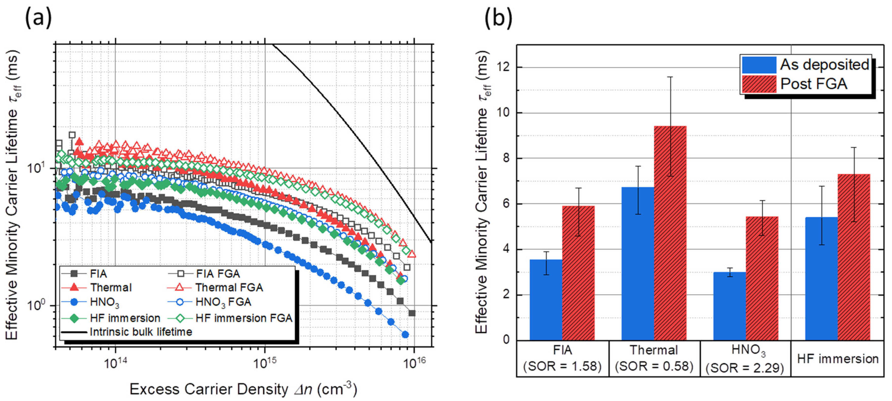
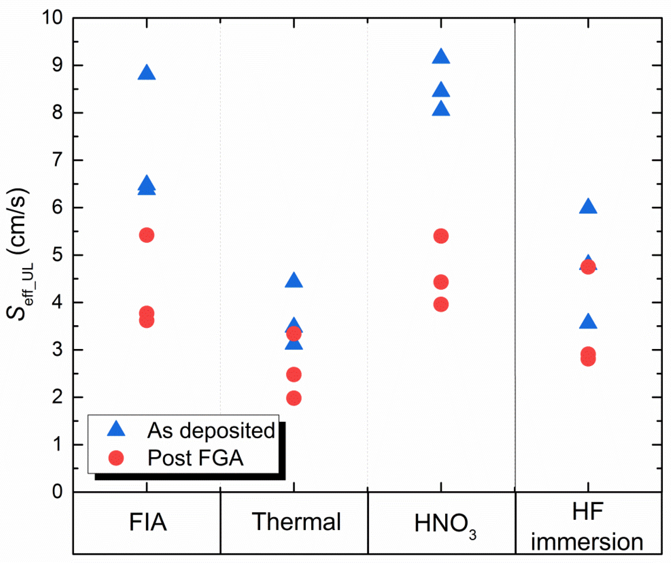
Figure 5a graphs τeff as a function of excess carrier density (∆n) for SiOx fabricated by FIA, thermal oxidation and HNO3 oxidation, both before and after FGA. After SiNx deposition, the samples anodised by FIA achieved an τeff of ~3.8 ms, which is higher than that of the wet-chemically oxidised wafers in HNO3 solution (2.8 ms), and lower than the τeff obtained for thermally-oxidised samples (7.0 ms) at ∆n = 1 × 1015 cm−3. This trend fits in well with the Seff_UL values extracted and graphed in Figure 6. The average Seff_UL for the FIA oxide was ~7.2 cm/s compared to 3.7 cm/s for the thermally-grown oxide and 8.6 cm/s for the oxide grown in HNO3. To correlate the surface passivation results with the sub-oxide ratios reported in Table 1, a bar chart showing the average τeff at ∆n = 1 × 1015 cm−3 for samples passivated by different SiOx and SiNx stack is presented in Figure 5b. It was observed that in the as-deposited form, the τeff increased with a decreasing sub-oxide ratio, confirming that the more stoichiometric tunnel oxides more effectively reduce recombination at the n-Si surfaces. This finding is consistent with previously-published results [15]. Since the chemical passivation is strongly influenced by the Si and SiOx interface, a more stoichiometric oxide at the transition region is expected to result in a lower interface trap density (Dit) and hence a lower surface recombination velocity.
Very low surface recombination velocities (4.8 cm/s at ∆n = 1 × 1015 cm−3) were achieved in the absence of a tunnel oxide (i.e., SiNx deposition following HF immersion). The τeff of these samples was higher and the Seff_UL was lower for all injection levels compared the samples which included a tunnel SiOx either grown by FIA or by HNO3 oxidation. This is most likely due to a Si-rich interface layer which was reported to be unintentionally deposited in the dual-mode plasma reactor used for this study even when using a recipe for a stoichiometric SiNx [35]. However, with the insertion of a tunneling thermal oxide layer at the interface, improvement of passivation can be seen, most likely due to the more O saturated Si bonds at the interface.
The effect of FGA on the passivation provided by SiOx/SiNx stack and by SiNx alone was also evaluated. It can be seen from Figure 5a,b that the τeff was increased for all samples after annealed in forming gas with reduction in Seff_UL also being observed. The improvement in passivation is presumably due to the release of H atoms during the FGA which diffuse into the Si and SiOx or SiNx interface to passivate the dangling Si atoms. Overall, the ultra-thin tunnel SiOx layer prepared by thermal oxidation provided the best passivation, followed by FIA oxide, then the oxide grown in HNO3. This result suggests that the FIA process can offer a low-cost alternative for forming ultra-thin tunnel SiOx layers for passivated contacts. The through-wafer oxidation can result in oxides of uniform thickness. However, as high temperatures (> 800 °C) are used to form poly-Si, the compositional structure of the FIA oxide and its passivation quality after high temperature annealing will be assessed in future experiments.
4. Conclusions
We have demonstrated the potential of using anodic SiOx formed by FIA as a tunneling oxide layer for passivated contacts for Si solar cells. The stoichiometry and passivation quality of these SiOx tunneling layers were compared to those formed by thermal oxidation and chemical oxidation in HNO3. It was shown that the fraction of Si-rich sub-oxides present in the FIA oxide layer was higher than detected in the thermally-oxidised film, but lower than that observed in the wet-chemical oxide, of a comparable thickness. Furthermore, the surface passivation provided by the interfacial SiOx correlated with the oxide stoichiometry with the SiOx layers containing more O-rich sub-oxides in the transition region resulting in lower recombination velocity at the Si/SiOx interface. Given the effective passivation provided by the FIA oxide and its controllability offered from the room-temperature anodisation process, it was concluded that FIA provides a robust way of fabricating uniform tunneling oxide layers for passivated contacts for Si solar cells. Uniformity is assured through the FIA process with the oxide growing to the same thickness because current flows though the wafer until the resistance is uniform across the surface. Future work will investigate the passivation provided by the FIA oxides capped with poly-Si and the effect of high temperature annealing on their properties.
Acknowledgments
The authors acknowledge the facilities, and the scientific and technical assistance at the UNSW Electron Microscope Unit (EMU) for STEM sample preparation; Bin Gong from UNSW Mark Wainwright Analytical Centre for XPS analysis and David Mitchell and Gilberto Casillas Garcia at the University of Wollongong (UOW) Electron Microscopy Centre for their assistance on STEM imaging and EDS line scan. The authors would also like to thank Udo Römer for proof reading.
Author Contributions
Jingnan Tong and Alison Lennon conceived and designed the experiments. Jingnan Tong performed the experiments, analyzed the data and wrote the paper. Sean Lim assisted with TEM sample preparation. Jingnan Tong and Alison Lennon discussed the results.
Conflicts of Interest
The authors declare no conflict of interest.
References
- Green, M.A.; Godfrey, R. MIS solar cell—General theory and new experimental results for silicon. Appl. Phys. Lett. 1976, 29, 610–612. [Google Scholar] [CrossRef]
- Bian, J.; Zhang, L.; Guo, W.; Wang, D.; Meng, F.; Liu, Z. Improved passivation effect at the amorphous/crystalline silicon interface due to ultrathin SiOx layers pre-formed in chemical solutions. Appl. Phys. Express 2014, 7, 065504. [Google Scholar] [CrossRef]
- Seif, J.P.; Descoeudres, A.; Filipič, M.; Smole, F.; Topič, M.; Holman, Z.C.; De Wolf, S.; Ballif, C. Amorphous silicon oxide window layers for high-efficiency silicon heterojunction solar cells. J. Appl. Phys. 2014, 115, 024502. [Google Scholar] [CrossRef]
- Ohdaira, K.; Oikawa, T.; Higashimine, K.; Matsumura, H. Suppression of the epitaxial growth of Si films in Si heterojunction solar cells by the formation of ultra-thin oxide layers. Curr. Appl. Phys. 2016, 16, 1026–1029. [Google Scholar] [CrossRef]
- Bullock, J.; Yan, D.; Cuevas, A.; Wan, Y.; Samundsett, C. n- and p-type silicon solar cells with molybdenum oxide hole contacts. Energy Procedia 2015, 77, 446–450. [Google Scholar] [CrossRef]
- Gad, K.M.; Vössing, D.; Richter, A.; Rayner, B.; Reindl, L.M.; Mohney, S.E.; Kasemann, M. Ultrathin titanium dioxide nanolayers by atomic layer deposition for surface passivation of crystalline silicon. IEEE J. Photovolt. 2016, 6, 649–653. [Google Scholar] [CrossRef]
- Feldmann, F.; Bivour, M.; Reichel, C.; Hermle, M.; Glunz, S.W. Passivated rear contacts for high-efficiency n-type Si solar cells providing high interface passivation quality and excellent transport characteristics. Sol. Energy Mater. Sol. Cells Part A 2014, 120, 270–274. [Google Scholar] [CrossRef]
- Glunz, S.; Feldmann, F.; Richter, A.; Bivour, M.; Reichel, C.; Steinkemper, H.; Benick, J.; Hermle, M. The irresistible charm of a simple current flow pattern—25% with a solar cell featuring a full-area back contact. In Proceedings of the 31st European Photovoltaic Solar Energy Conference and Exhibition, Hamburg, Germany, 14–18 September 2015; pp. 259–263. [Google Scholar]
- Yan, D.; Cuevas, A.; Bullock, J.; Wan, Y.; Samundsett, C. Phosphorus-diffused polysilicon contacts for solar cells. Sol. Energy Mater. Sol. Cells 2015, 142, 75–82. [Google Scholar] [CrossRef]
- Upadhyaya, A.D.; Ok, Y.W.; Chang, E.; Upadhyaya, V.; Madani, K.; Tate, K.; Rounsaville, B.; Choi, C.J.; Chandrasekaran, V.; Yelundur, V.; et al. Ion-implanted screen-printed n-type solar cell with tunnel oxide passivated back contact. IEEE J. Photovolt. 2016, 6, 153–158. [Google Scholar] [CrossRef]
- Stodolny, M.K.; Lenes, M.; Wu, Y.; Janssen, G.J.M.; Romijn, I.G.; Luchies, J.R.M.; Geerligs, L.J. n-Type polysilicon passivating contact for industrial bifacial n-type solar cells. Sol. Energy Mater. Sol. Cells 2016, 158, 24–28. [Google Scholar] [CrossRef]
- Yang, G.; Ingenito, A.; Isabella, O.; Zeman, M. IBC c-Si solar cells based on ion-implanted poly-silicon passivating contacts. Sol. Energy Mater. Sol. Cells 2016, 158, 84–90. [Google Scholar] [CrossRef]
- Young, D.L.; Lee, B.G.; Fogel, D.; Nemeth, W.; LaSalvia, V.; Theingi, S.; Page, M.; Young, M.; Perkins, C.; Stradins, P. Gallium-doped poly-Si:Ga/SiO2 passivated emitters to n-Cz wafers with iV oc >730 mv. IEEE J. Photovolt. 2017, 7, 1640–1645. [Google Scholar] [CrossRef]
- Haase, F.; Kiefer, F.; Schäfer, S.; Kruse, C.; Krügener, J.; Brendel, R.; Peibst, R. Interdigitated back contact solar cells with polycrystalline silicon on oxide passivating contacts for both polarities. Jpn. J. Appl. Phys. 2017, 56, 08MB15. [Google Scholar] [CrossRef]
- Moldovan, A.; Feldmann, F.; Zimmer, M.; Rentsch, J.; Benick, J.; Hermle, M. Tunnel oxide passivated carrier-selective contacts based on ultra-thin SiO2 layers. Sol. Energy Mater. Sol. Cells 2015, 142, 123–127. [Google Scholar] [CrossRef]
- Feldmann, F.; Steinhauser, B.; Tutsch, L.; Kluska, S.; Hermle, M.; Glunz, S. Status and Industrial Perspectives of Topcon. Proceedings of Materials Research Society Fall Meetings & Exhibit, Boston, MA, USA, 26 November–1 December 2017. [Google Scholar]
- Ling, Z.P.; Xin, Z.; Ke, C.; Buatis, K.J.; Duttagupta, S.; Lee, J.S.; Lai, A.; Hsu, A.; Rostan, J.; Stangl, R. Comparison and characterization of different tunnel layers, suitable for passivated contact formation. Jpn. J. Appl. Phys. 2017, 56, 08MA01. [Google Scholar] [CrossRef]
- Fehlner, F.P. Formation of ultrathin oxide films on silicon. J. Electrochem. Soc. 1972, 119, 1723–1727. [Google Scholar] [CrossRef]
- Azman, A.; Ayub, R.; Arshad, M.M.; Norhafiezah, S.; Fathil, M.; Kamarudin, M.; Nurfaiz, M.; Hashim, U. Controlling growth rate of ultra-thin silicon dioxide layer by incorporating nitrogen gas during dry thermal oxidation. In Proceedings of the 2014 IEEE International Conference on Semiconductor Electronics (ICSE2014), Kuala Lumpur, Malaysia, 27–29 August 2014; pp. 392–395. [Google Scholar]
- Adams, A.; Smith, T.; Chang, C. The growth and characterization of very thin silicon dioxide films. J. Electrochem. Soc. 1980, 127, 1787–1794. [Google Scholar] [CrossRef]
- Kobayashi, A.H.; Maida, O.; Takahashi, M.; Iwasa, H. Nitric acid oxidation of Si to form ultrathin silicon dioxide layers with a low leakage current density. J. Appl. Phys. 2003, 94, 7328–7335. [Google Scholar] [CrossRef]
- Kobayashi, H.; Imamura, K.; Kim, W.B.; Im, S.S. Nitric acid oxidation of Si (NAOS) method for low temperature fabrication of SiO2/Si and SiO2/SiC structures. Appl. Surf. Sci. 2010, 256, 5744–5756. [Google Scholar] [CrossRef]
- Grant, N.E.; McIntosh, K.R. Low surface recombination velocity on (100) silicon by electrochemically grown silicon dioxide annealed at low temperature. IEEE Electron Device Lett. 2010, 31, 1002–1004. [Google Scholar] [CrossRef]
- Grant, N.E.; McIntosh, K.R. Passivation of a (100) silicon surface by silicon dioxide grown in nitric acid. IEEE Electron Device Lett. 2009, 30, 922–924. [Google Scholar] [CrossRef]
- Lennon, A.; Yeo, J.; Lu, P.H.; Sun, Y.; Wang, X.; Lu, Z.; Li, Y.; Vais, V. Field-induced anodization for silicon solar cell passivation. In Proceedings of the 2013 IEEE 39th Photovoltaic Specialists Conference (PVSC), Tampa, FL, USA, 16–21 June 2013; pp. 1257–1259. [Google Scholar]
- Vais, V.; Lennon, A.J.; Wenham, S.R.; Ji, J.J.; Wenham, A.M. Metal contact scheme for solar cells. WO Patent WO/2012/000015, 12 11 2012. [Google Scholar]
- Cui, J.; Wang, X.; Opila, R.; Lennon, A. Light-induced anodisation of silicon for solar cell passivation. J. Appl. Phys. 2013, 114, 184101. [Google Scholar] [CrossRef]
- Tong, J.; Wang, X.; Ouyang, Z.; Lennon, A. Ultra-thin tunnel oxides formed by field-induced anodisation for carrier-selective contacts. Energy Procedia 2015, 77, 840–847. [Google Scholar] [CrossRef]
- Cui, J.; Grant, N.; Lennon, A. Effective surface passivation of p-type crystalline silicon with silicon oxides formed by light-induced anodisation. Appl. Surf. Sci. 2014, 323, 40–44. [Google Scholar] [CrossRef]
- Tong, J.; Wang, X.; Lennon, A. Requirements to achieve field-induced anodisation for silicon surface passivation. Energy Procedia 2014, 55, 855–864. [Google Scholar] [CrossRef]
- Kern, W. Cleaning solutions based on hydrogen peroxide for use in silicon semiconductor technology. RCA Rev. 1970, 31, 187–206. [Google Scholar]
- Sze, S.M. Semiconductor Devices: Physics and Technology, 2nd ed.; John Wiley & Sons: New York, NY, USA, 2002. [Google Scholar]
- Richter, A.; Glunz, S.W.; Werner, F.; Schmidt, J.; Cuevas, A. Improved quantitative description of auger recombination in crystalline silicon. Phys. Rev. B 2012, 86, 165202. [Google Scholar] [CrossRef]
- Parkhutik, V. Modeling of the electrochemical anodization of silicon: State-of-the-art and perspectives. In Proceedings of the Third International Symposium on Pits and Pores: Formation, Properties and Significance for Advanced Luminescent Materials, Honolulu, HI, USA, 6 October 2004. [Google Scholar]
- Tong, J.; To, A.; Lennon, A.; Hoex, B. Unintentional consequences of dual mode plasma reactors: Implications for upscaling lab-record silicon surface passivation by silicon nitride. Jpn. J. Appl. Phys. 2017, 56, 08MB12. [Google Scholar] [CrossRef]
Figure 1.
Schematic diagram showing the field-induced anodisation (FIA) process.

Figure 2.
Thickness of the SiOx layer formed by immersion in 0.5 M H2SO4 and FIA under different anodisation conditions. The thickness was measured using ellipsometry at 5 different points across the wafer and is represented as a mean with the error bars representing the standard deviation [28].
Figure 2.
Thickness of the SiOx layer formed by immersion in 0.5 M H2SO4 and FIA under different anodisation conditions. The thickness was measured using ellipsometry at 5 different points across the wafer and is represented as a mean with the error bars representing the standard deviation [28].
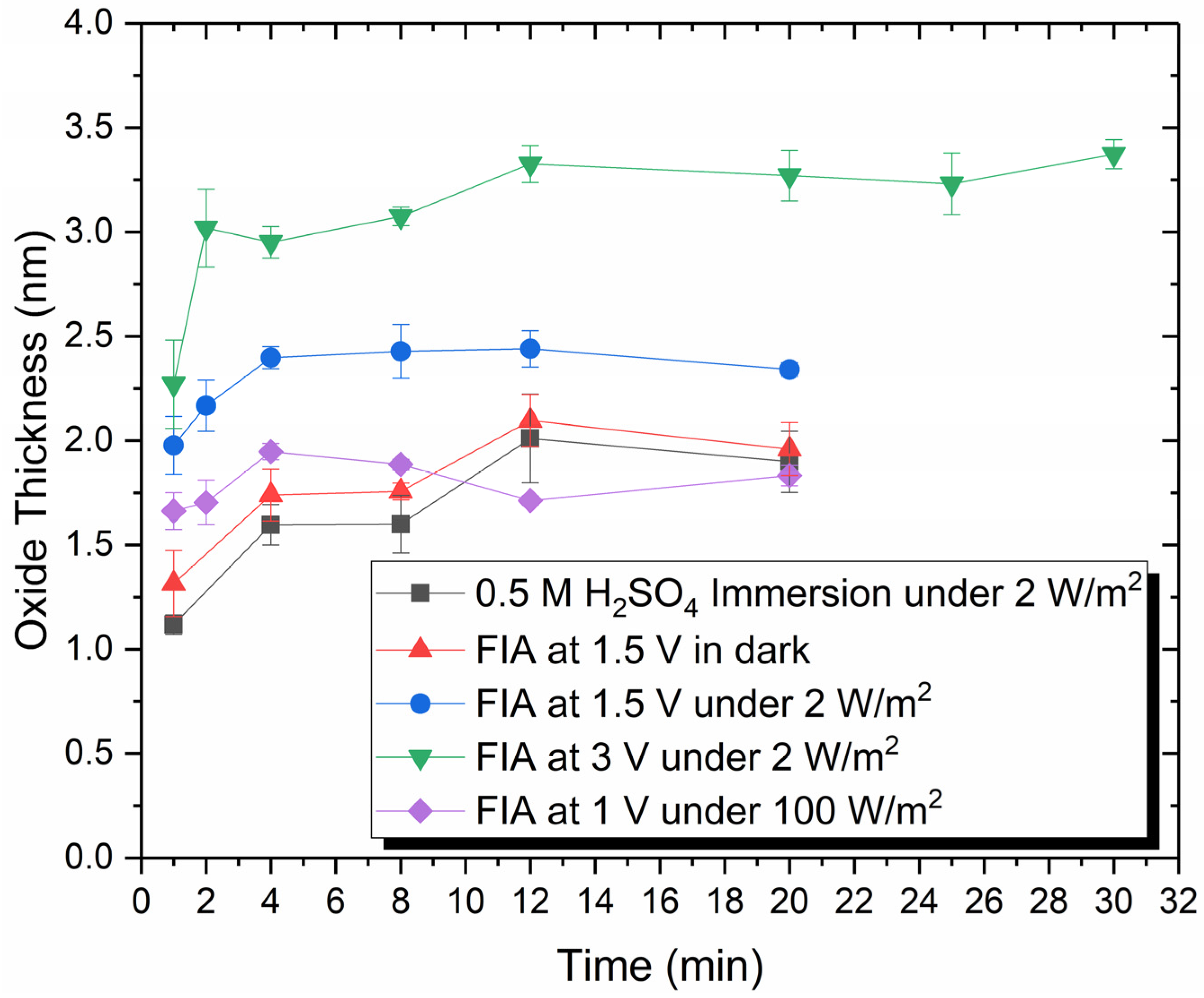
Figure 3.
(a) High-resolution transmission electron microscopy images of an anodic oxide film formed by FIA using pulsed anodisation (50% positive cycle at 1 V and 50% negative cycle at −1 V) for 20 min under an illumination of 100 W/m2, inset shows a higher resolution view. (b) energy dispersive X-ray spectroscopy (EDS) line scan through the oxide layer showing an O peak in the oxide layer.

Figure 4.
X-ray photoelectron spectroscopy (XPS) spectral decomposition of the Si 2p spectrum showing the sub-oxide peaks for: (a) oxide grown by immersion alone; (b) FIA oxide anodised at constant voltage of 1.0 V for 20 min; (c) thermally-grown thin oxide; and (d) wet-chemical oxide grown in HNO3. A higher resolution view of the sub-oxide region of the spectrum is also shown for each oxide.

Figure 5.
(a) Values of τeff measured as a function of ∆n for n-Si wafers symmetrically passivated by SiOx and SiNx stack before (solid symbols) and after (open symbols) forming gas anneal (FGA). The ∆n dependent τeff for samples passivated with thin FIA SiOx (dark-grey squares) capped with SiNx layer is compared to those passivated by thin thermal SiOx (red triangles) and HNO3 SiOx (blue circles) when capped with SiNx. The τeff of samples passivated with a single layer SiNx after hydrofluoric acid (HF) immersion (green diamonds) is shown for reference. (b) Values of τeff obtained at ∆n = 1 × 1015 cm−3 for samples passivated with different thin SiOx and SiNx stacks and with a single layer SiNx before and after FGA. Three samples were measured for each group with the solid columns showing the mean and error bars representing the minimum and maximum. The sub-oxide ratio (SOR) is included in the category label with the oxide preparation method.

Figure 6.
Values of Seff_UL extracted at ∆n = 1 × 1015 cm−3 for n-Si samples passivated with ultra-thin SiOx formed by FIA, thermal oxidation and wet-chemical HNO3 oxidation followed by a SiNx capping. Data presented includes three samples per oxidation condition. The values of Seff_UL for samples passivated by a single layer SiNx after HF immersion are also shown.


Table 1.
Oxide thickness (determined from ellipsometry using a refractive index for thermal oxide of 1.46) for the SiOx layer grown using different methods and the atomic percentage of the Si1+, Si2+ and Si3+ peaks obtained from XPS with the calculated sub-oxide ratio Si1+/(Si2+ + Si3+).
Table 1.
Oxide thickness (determined from ellipsometry using a refractive index for thermal oxide of 1.46) for the SiOx layer grown using different methods and the atomic percentage of the Si1+, Si2+ and Si3+ peaks obtained from XPS with the calculated sub-oxide ratio Si1+/(Si2+ + Si3+).
| Oxide | Thickness (nm) | Si1+ | Si2+ | Si3+ | Si1+/(Si2+ + Si3+) |
|---|---|---|---|---|---|
| FIA (1.0 V) | 1.8 | 1.28 | 0.46 | 0.35 | 1.58 |
| Thermal | 1.6 | 0.48 | 0.47 | 0.36 | 0.58 |
| HNO3 | 1.6 | 1.49 | – | 0.65 | 2.29 |
© 2018 by the authors. Licensee MDPI, Basel, Switzerland. This article is an open access article distributed under the terms and conditions of the Creative Commons Attribution (CC BY) license (http://creativecommons.org/licenses/by/4.0/).
Share and Cite
MDPI and ACS Style
Tong, J.; Lim, S.; Lennon, A. Tunnel Oxides Formed by Field-Induced Anodisation for Passivated Contacts of Silicon Solar Cells. Coatings 2018, 8, 81. https://doi.org/10.3390/coatings8020081
AMA Style
Tong J, Lim S, Lennon A. Tunnel Oxides Formed by Field-Induced Anodisation for Passivated Contacts of Silicon Solar Cells. Coatings. 2018; 8(2):81. https://doi.org/10.3390/coatings8020081
Chicago/Turabian StyleTong, Jingnan, Sean Lim, and Alison Lennon. 2018. "Tunnel Oxides Formed by Field-Induced Anodisation for Passivated Contacts of Silicon Solar Cells" Coatings 8, no. 2: 81. https://doi.org/10.3390/coatings8020081
Note that from the first issue of 2016, this journal uses article numbers instead of page numbers. See further details here.