Study of Topography and Distribution State of the Nanoscale Passivation Film on a Rough Tinplate Surface

School of Chemistry and Chemical Engineering, Harbin Institute of Technology, Harbin 150001, China
*
Author to whom correspondence should be addressed.
Coatings 2018, 8(3), 94; https://doi.org/10.3390/coatings8030094
Submission received: 10 January 2018
/
Revised: 20 February 2018
/
Accepted: 1 March 2018
/
Published: 6 March 2018
Abstract
:Topography observation of the nanoscale passivation film on tinplate using a scanning electron microscope and an electro-optical surface profilometer showed that it was difficult to observe the true topography because of the high surface roughness of the tinplate. Topography observation using a profilometer on bright tin plating with low surface roughness and work function measurement on tinplate surface using a Scanning Kelvin Probe Microscope (SKPM) were then carried out to solve the problem. The results indicated that there was a thin chemical passivation film distributed uniformly in different areas of microscopic bulges and valleys on the tinplate surface, and the film became more uniform with longer passivation time. In comparison, the electrolytic passivation film was thick, and the distribution uniformity was poorer. Specifically, the film was thicker on microscopic bulges and thinner in microscopic valleys, and this was worse with longer passivation time. Thus, the difference in performances of the corrosion and paint adhesion of the tinplate treated with different passivation processes can be explained in terms of the topography and distribution state of the passivation film.
1. Introduction
The passivation film that forms on the surface of tinplate via chemical or electrochemical reaction plays a vital role during tinplate storage, transportation, and use [1,2,3]. On one hand, the passivation film can block the diffusion and penetration of oxygen and corrosive media (such as chloride ions and sulfur ions) into the interior of the tinplate, thereby enhancing the oxidation resistance and corrosion resistance of the tinplate. On the other hand, the film can play a role in connecting the tinplate and the coatings or paint films when producing cans to improve adhesion [1,4,5,6]. Thus, the performance of the tinplate is directly related to the properties of the passivation film.
The fundamental factors that affect the performance of the passivation film on the tinplate depend on the properties of the passivation film itself. Specifically, the performance depends on the composition and structure of the passivation film [7,8,9]. Meanwhile, the topography and distribution state of the film on the surface also has an important impact. Obviously, a thicker film results in better corrosion resistance, although it is also believed that a film that is too thick results in poor paint adhesion [1,10]. It is essential for a passivation film to be uniformly thick because in a corrosive environment, if the thickness is not uniform, it is likely that corrosion microcells will develop between the local regions without film (or with a thinner film covering) and the regions covered with thicker film because of the different surface potential between the regions; this then causes pitting corrosion [11,12].
However, the passivation film is very thin and its thickness is on the nanoscale [2,13]. Also, the colorless and transparent film will not change the appearance of the tinplate and is difficult to observe with the naked eye [3]. Furthermore, the roughness of the tinplate substrate under the film is much larger than the thickness of the film [14]. Therefore, it is difficult to observe the true surface topography and the distribution conditions of the film using common microscopic methods. Although transmission electron microscopy has been used to observe the structure and composition of the passivation films on tinplate [13], the sample preparation of film stripping is complicated. Thus, studying the film topography and distribution state of the tinplate surface is highly difficult and has rarely been reported in previous studies. In this paper, we report a detailed study of the above problems using new methods with the aim of understanding more about the nanoscale passivation film on tinplate, since the film is invisible yet vital to tinplate performance.
2. Materials and Methods
2.1. Material and Surface Preparation
The base steel of the tinplate was a one-step cold-rolled steel sheet with a thickness of 0.17 mm, which was cut into 100 mm × 70 mm coupons. Prior to electroplating, the samples were subjected to electrolytic degreasing by immersing them in a 60 °C aqueous solution of 20 g/L NaOH and electrolyzing them with a cathodic current density of 3 A/dm2 for 30 s; they were then rinsed with deionized water for 1 min. The samples were then immersed in a 60 °C aqueous solution of 10 wt % H2SO4 and electrolyzed with a cathodic current density of 3 A/dm2 for 5 s; the samples were then rinsed with deionized water for 30 s.
After the pretreatment process, the samples were electroplated by immersing them in a 45 °C plating bath that was complexed with 15 g/L tin methanesulfonate, 45 mL/L methanesulfonic acid, 45 mL/L additive (Ronastan TP-G7, The Dow Chemical Company, Midland, MI, USA), and 25 mL/L antioxidant (Ronastan TP-G7, The Dow Chemical Company). The samples were electrolyzed with a cathodic current density of 1.4 A/dm2 for 33 s to form a plating with approximately 2.8 g/m2 tin. The sample was then rinsed with deionized water for 1 min and dried with hot air. A reflowing treatment of the sample after drying was carried out via induction heating at a power of 630 W for 0.64 s, followed by quenching in 50 °C deionized water. The sample was then rinsed with deionized water for 30 s and dried with hot air to finish the surface preparation of the tinplate sample.
Bright tin plating was prepared by immersing the pretreated sample in a 25 °C electroplating bath that was complexed with 15 g/L tin methanesulfonate, 100 mL/L methanesulfonic acid, and 20 mL/L self-developed bright tin additive; the sample was electrolyzed with a cathodic current density of 2 A/dm2 for 30 min. During the plating process, the solution was stirred using a magnetic stirrer to avoid the formation of pinholes that can be caused by hydrogen evolution on the cathode surface. The sample was then rinsed with deionized water for 1 min and dried with hot air to finish the surface preparation of bright plating. In particular, reflowing was not needed for the bright tin plating.
2.2. Passivation Treatment
Chemical passivation was carried out by immersing the prepared sample in a 45 °C aqueous solution of 25 g/L sodium dichromate with a pH of 4.2 (adjusted with an aqueous solution of NaOH and CrO3) for different lengths of time followed by rinsing with deionized water for 1 min and drying with hot air. The prepared sample was immersed in the same solution with chemical passivation and electrolyzed with a cathodic current density of 1 A/dm2 for different lengths of time followed by rinsing with deionized water for 1 min and drying with hot air to carry out the electrolytic passivation treatment.
2.3. Characterization
A field emission scanning electron microscope (Quanta200 FEG, Thermo Fisher Scientific Inc., Hillsboro, OR, USA) was used to observe the surface topography of the tinplate. A three-dimensional electro-optical surface profilometer (WGL, Shanghai Jing Ke Industrial Co., Ltd., Shanghai, China) was used to investigate the geometrical topography of the tinplate. A scanning Kelvin probe microscope (SKP100E, Princeton Instruments, Trenton, NJ, SUA) with a 2-mm diameter platinum electrode as a probe was used to measure the work function of the tinplate; the tip of the probe was kept at a constant distance of 85 μm from the surface of the test sample to measure the work function difference between the sample surface and the platinum electrode tip.
3. Results
3.1. Topography of the Passivation Film on the Tinplate
3.1.1. SEM Topography
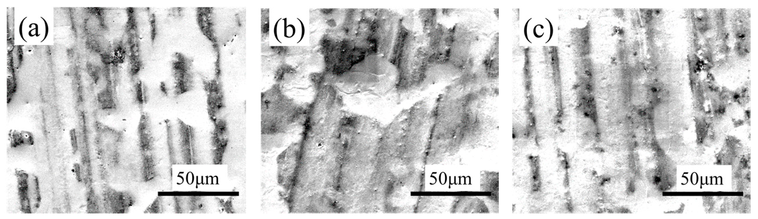
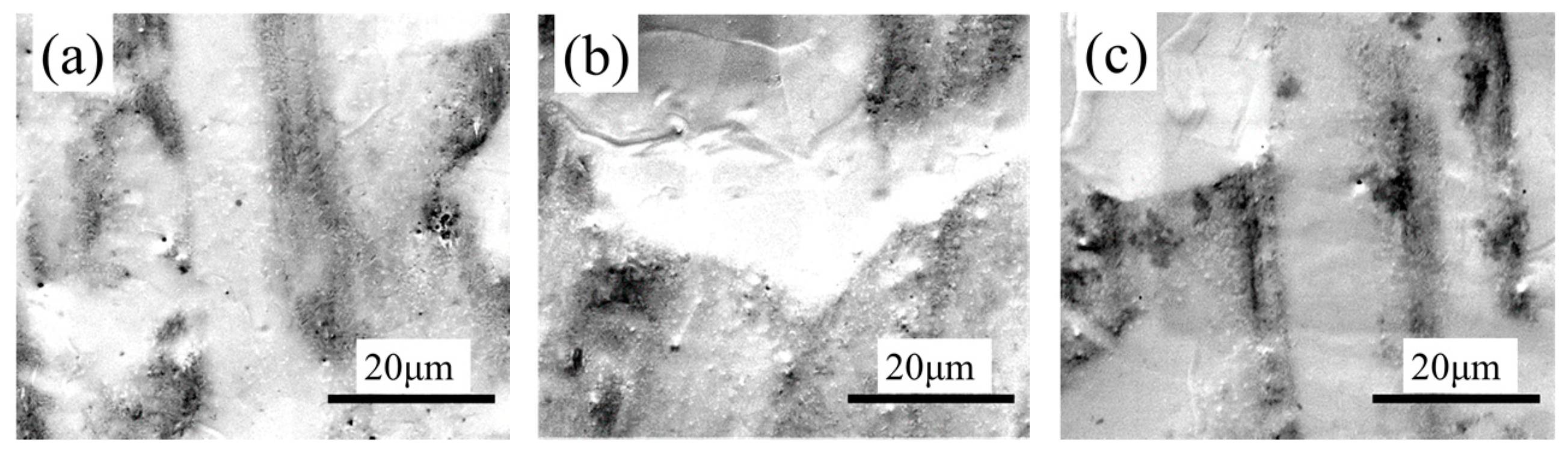
The surface topography of the tinplate treated with reflowing was observed using scanning electron microscopy (SEM, Quanta200 FEG, Thermo Fisher Scientific Inc., Hillsboro, OR, USA), and the results are shown in Figure 1a. The surface of the tinplate after reflowing is uneven; there are numerous striations and some pits on the surface that should be the roll marks arose from the rolling process of the base steel sheet [15,16]. These marks will still exist on the surface when the tin plating is not so thick. The surface topography of the tinplate was not significantly changed after treatment with chemical passivation (Figure 1b) and electrolytic passivation (Figure 1c). The surface topography of the tinplate was then observed at a higher magnification (Figure 2). However, there were still no significant changes to the surface topography of the tinplate observed before (Figure 2a) or after (Figure 2b,c) the passivation treatment. This could be because the passivation film is extremely thin, with a thickness that is on the nanoscale, whereas the substrate under the film has a high roughness itself, which is much greater than the thickness of the film. Therefore, the film topography can be extremely susceptible to the substrate topography and can be difficult to observe using SEM. In light of this, test methods need to be sought that can reflect the changes of the surface topography before and after passivation.
3.1.2. Geometrical Topography
An electro-optical surface profilometer (a well-known tool for surface profilometry with high resolution) is based on phase-shift interferometry; it can be used for quickly measuring the three-dimensional geometrical topography of a specimen surface without contacting the sample or damaging the surface of the specimen; furthermore, the surface roughness can be obtained [17,18,19,20,21]. Figure 3 shows the three-dimensional geometrical topography of the tinplate as determined using different processes. As a further support data, the value of Ra was calculated by the computer connected to the profilometer. The calculation method was to take a point in the test area, and calculate the data of roughness, Ra, in z-axis direction of the cross-section (along the x-axis direction) and the longitudinal section (along the y-axis direction) of this point. The resulting value of Ra is the statistical calculation result of multiple points in the test area, and it is the average of the surface roughness in the test area. Then, we compared the average data of Ra by statistical analyses. The average values of Ra were obtained using data from nine different test areas by random selection on the surface of the sample. The maximum and minimum values were removed and are not listed in the table.
As seen in Figure 3, there are striations and pits on the surface of the tinplate surface. The changes to the surface geometrical topography are not remarkable before passivation (Figure 3a) and after treatment with chemical passivation (Figure 3b), and the Ra average value does not change significantly (Table 1), which may be because a film that is uniformly thick has formed on the basis of the original profile of the substrate so the surface roughness value has not changed significantly. After electrolytic passivation, many high bulges can be seen in local regions of the tinplate surface (Figure 3c); also, the film is thicker compared to the chemical passivation film, and the pits and striations are still visible. Although general variations in the surface profile are not significant, the surface roughness (Ra) increased remarkably compared to the non-passivated and chemical passivated tinplate samples. This may be because the thickness of the electrolytic passivation film is not as uniform as the chemical passivation film; also, in some regions, the film is thicker, whereas in some other regions, the film is thinner or there is no film on the tinplate surface. In this last case, the result is that the roughness increases significantly.
Figure 3 provides stereo images and visualizes the surface geometrical topography to reflect the changes in the surface topography of the tinplate before and after passivation. Additionally, it is necessary to verify the fact that there are striations and pits on the tinplate surface. Roughness data confirm that the surface roughness of the tinplate is large. Using this test method, the thickness of the electrolytic passivation film is found to be thicker than that of the chemical passivation film, although the uniformity is poorer. It is worth noting that, because of the large surface roughness of the tinplate before passivation, the extremely thin film layer that formed is greatly influenced by the substrate profile. To better observe the surface topography and to verify the above statement, it is necessary to reduce the surface roughness of the tinplate.
3.2. Topography of the Passivation Film on Bright Tin Plating
3.2.1. SEM Topography
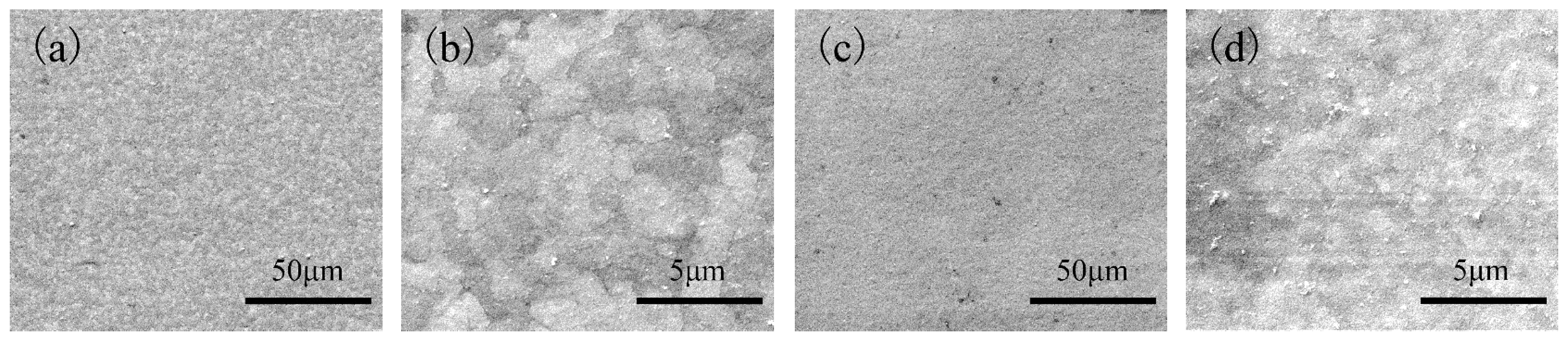
We prepared a tinplate with a smooth tin surface on which the passivation treatment was carried out, and we then characterized the topography of the passivation film to reduce the influence of the surface roughness of the tinplate on the passivation film. Using the bright tinning process described in Section 2.1, electroplating was carried out by adding a suitable brightener to the plating solution to obtain a bright tinplate, as shown in Figure 4a. The lower part of the image in Figure 4a is the real object, and the upper part is the reflection of the object in the bright tinplated surface. The high definition reflection indicates that the tinplate has a good brightness and low roughness. It can be seen from Figure 4b,c that the topography of the plating is flat and uniform, and no microscopic bulges or pits are observed. Thus, a smooth tin surface with low roughness was obtained.
The surface topography of the bright tin plating treated with chemical and electrolytic passivation observed using scanning electron microscopy is shown in Figure 5. The grain boundaries of the tin plating after chemical passivation (Figure 5b) become indistinct compared to that of the tin plating before passivation (Figure 4c), and the grain boundaries become less apparent and cannot even be seen at higher magnification after electrolytic passivation (Figure 5d). These observations indicate that the surface of the tin plating has certainly been covered with a film. Although the variation of the surface topography before and after passivation could be characterized using scanning electron microscopy, the actual topography of the passivation film could still not clearly be observed in the SEM images, even when a smooth substrate with a low roughness was used. Because of this, using an electro-optical surface profilometer should be considered for testing.
3.2.2. Geometrical Topography
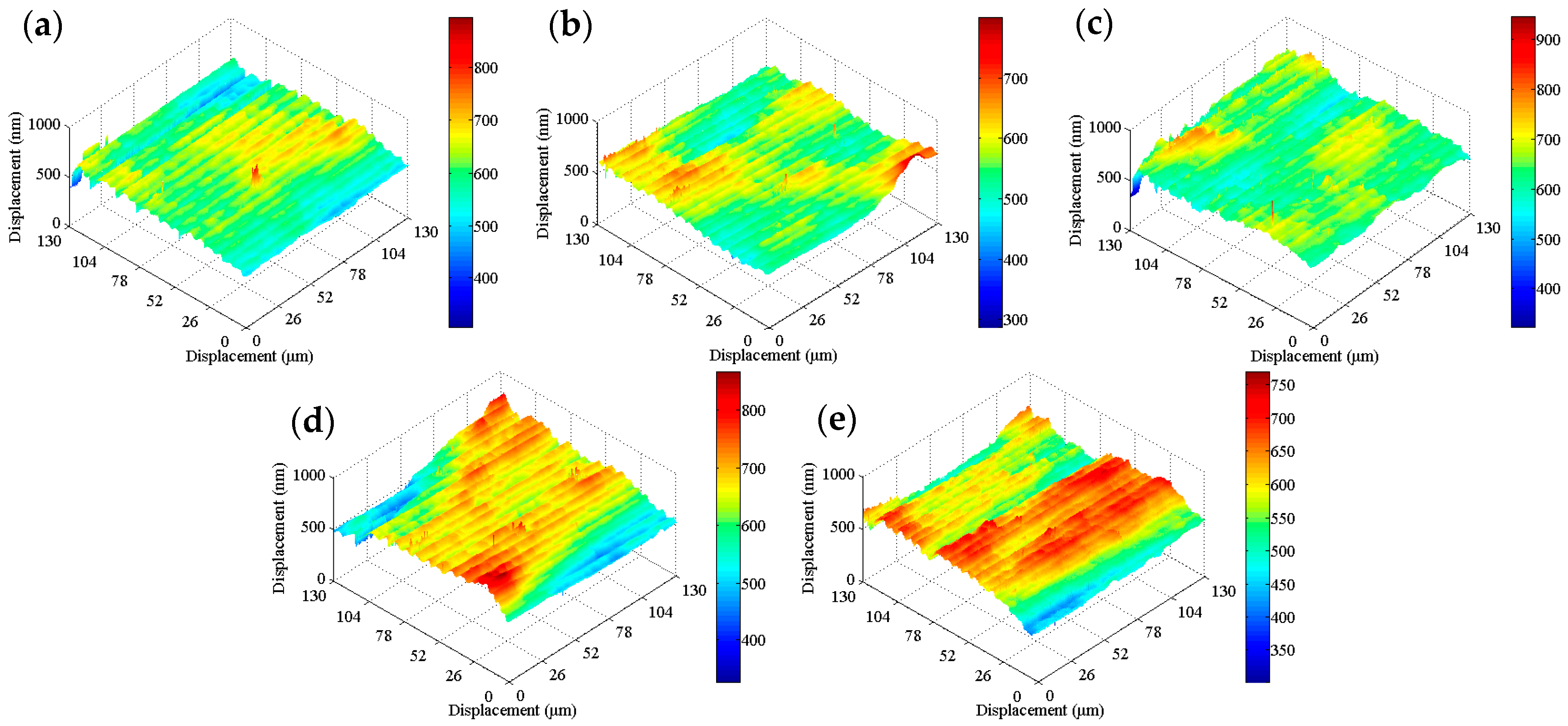
The three-dimensional geometric topography of the bright tin plating before and after passivation was characterized using the profilometer, and the results are shown in Figure 6. Also, the corresponding surface roughness is listed in Table 2. As seen in Figure 6a, there are regular and uniformly distributed striations on the bright tin plating surface, and the size scale of the striations are tiny. Thus, the value of the surface roughness (Ra) is only 22.41 nm on average, and the standard deviation is 1.81 nm (Table 2). To a certain extent, the average roughness and standard deviation represent the surface smoothness, and thus the bright tin plating has a more smooth and uniform surface compared to the conventional tinplate.
Figure 6b shows that the striations on the bright tin surface can still be observed after 3 s of chemical passivation. In contrast, the valleys of the striations become shallow, indicating that there is also a passivation film formed in the valley, and thus the striations become indistinct. The surface profile is raised in local regions along the bulges of the striations, and this indicates the formation of a thick film in those regions. The surface roughness (average Ra) and standard deviation (Table 2) slightly increase after chemical passivation, indicating that the passivation film did not grow uniformly along the profile of the original tin surface. The film is thicker on the bulges of the striations but thinner in the valleys of the striations; nevertheless, the thickness of the film itself is very thin, and so the roughness did not significantly increase. With longer chemical passivation time, the film thickness was more uniform (Figure 6c and Table 2). Also, when the sample was passivated for 6 s, the roughness decreased compared to that shown in Figure 6b, and this indicates that it is helpful to prolong the passivation time to enhance the uniform distribution of the film thickness.
The geometrical topography of the bright tin surface treated with electrolytic passivation for 3 s changes significantly, as shown in Figure 6d. There are large differences in the thickness of the passivation film that formed in different regions; specifically, the film is thicker on the bulges and thinner in the valleys of the striations, and this results in a significant increase in the surface roughness, as noted in Table 2. With the electrolytic passivation time extended from 3 s to 6 s, the film thickness is obviously increased, the distribution is less uniform, and the surface roughness is further increased, as seen in Figure 6e and Table 2. Compared to the chemical passivation film, although the thickness of the electrolytic passivation film increased significantly, the distribution uniformity is poorer, as seen in the surface topography and roughness of the tin plating.
Using the profilometer, the three-dimensional geometrical topography and roughness were tested on the surface of the bright tin plating. The results show that the changes in the topography before and after passivation were clearly reflected, and hence the problem regarding the influence of the large surface roughness of the conventional tinplate was effectively solved. Thus, the topography and distribution state of the film obtained via different passivation processes were measured.
3.3. Surface Work Function and its Distribution State
Scanning Kelvin probe microscopy (SKPM) is a noncontact and nondestructive analysis method that can be used to measure the work function on the surface of the sample; the scan area is on the macroscopic scale to provide more universal surface information of the sample [22,23,24]. There can be changes in the work function between the tinplate surfaces before and after passivation, and these changes are likely to relate to the thickness and uniformity of the passivation film [23,25,26]. Therefore, detecting the work function of the tinplate can be used to indirectly characterize the thickness and uniformity of the passivation film.
3.3.1. Relationship between Work Function Data and Passivation Film Thickness
The energy of an electron in the metal M is given by the electrochemical potential, , and can be written as the sum of the chemical potential () and the inner potential () (also called the Galvani potential) [27]. The inner potential includes two parts: the Volta (or outer) potential () and the surface potential () [28]. Formula (1) is expressed as follows:
The work function () is defined as the minimum work that is required to bring an electron from within the sample to a position just outside the sample [29]. When the metal M is uncharged, the Volta potential () can be zero, and as a result, the work function of the metal M can be formulated as [27,29]:
Substituting Formula (2) into Formula (1), yields:
In a metal or semiconductor, the Fermi energy is equivalent to the electrochemical potential of the electron [28]:
when , the work function and the Fermi energy are equal but numerically opposite to each other. In other words, the work function is equal to the difference between the vacuum level at the zero potential reference point and the Fermi level [23,30]. According to the above analysis, a schematic diagram of the Scanning Kelvin Probe Microscope (SKPM) test was drawn and is shown in Figure 7a.
In Figure 7a, and are the Fermi energies of the probe and sample, respectively, and and are the electric work functions of the probe and the sample, respectively. Platinum was used as the probe material; its work function is higher than that of most of the metal materials, and its Fermi energy and electrochemical potential are lower [31]. As shown in Figure 7b, when the probe and sample were connected with a wire, the electron flowed from the sample to the probe because the electrochemical potential of the electron in the sample was higher until the electrochemical potentials and the Fermi energies of the sample and probe became equal and resulted in both the Fermi and vacuum levels of the sample and the probe moving without variation relative to the positions of one another [28,32]. Then the probe surface was negatively charged, and the Volta potential () was generated; the sample surface was positively charged, and the Volta potential () was also generated, so that a contact potential difference () was generated.
At that time,
According to Formula (3),
The work function difference () between the sample and the probe is:
Formulas (5) and (8) were substituted into Formula (7) to deduce the relationship between the work function difference and the contact potential difference as Formula (9):
In the test mode, (Figure 7c), an external voltage (V) was applied using the instrument with the value equal to the opposite number of the contact potential difference () to make the surface charge of the probe and the sample equal to zero. The instrument recorded the value of the external voltage (V) and then was used to calculate the work function difference between the sample and the probe [23,29,30]. Therefore, the work function difference between the sample and the probe can be measured via the SKP method. The values obtained using the SKP method are always negative, and a more negative value indicates a lower work function of the sample.
From the definition of the work function, it becomes more difficult for the electron to escape from the surface of the tinplate when the surface is covered by a film and is in a passivated state after the passivation treatment. When the passivation film that covers the surface is thicker, it is more difficult for the electron to escape from the surface, and thus the work function is higher. In contrast, when the film is thinner, the work function is lower. Therefore, without considering other factors, it can be considered that when the work function difference measured via the SKP method is more negative, the passivation film is thinner, whereas when the work function is more positive, the passivation film is thicker.
3.3.2. Distribution State of the Work Function on the Tinplate Surface
SKP tests were carried out on the tinplate samples before and after passivation using different treatment processes, and the results are shown in Figure 8. The work function of the non-passivated tinplate (Figure 8a) was mainly distributed between −0.65 and −0.55 eV. The uneven distribution of the work function on the surface of the tinplate indicates that the surface state was not uniform after reflowing. This may be because in the reflowing process in which the steel was heated via magnetic introduction, the distribution of the magnetic field on the steel surface was not absolutely uniform because it was affected by the surface evenness of the steel and the distribution state of the magnetic induction loop. There were differences in different areas on the surface of the steel in the degree of heat so that the oxides of tin were generated in different oxidation states in different areas of the surface. In addition, the steel surface state before reflowing may not be uniform. Thus, the states in different areas of the tinplate surface were not absolutely uniform, and hence the distribution of the work function was not uniform.
According to the passivation mechanism [33], further oxidation of SnOx () generated during the reflowing process and reduction of Cr(VI) occurred simultaneously in the chemical passivation process, and then the passivation film formed on the surface of the tinplate; this resulted in an increase in the work function. Further oxidation of SnOx caused the oxidation state of tin in different areas on the tinplate surface to be uniform, and this resulted in a more uniform distribution of the work function on the surface. Figure 8b shows that the work function of the tinplate after 3 s of chemical passivation was mainly distributed in the range of approximately −0.61 to −0.54 eV, and this generally increased slightly, although there was no obvious improvement in the distribution uniformity. Combined with the images shown in Figure 6b, when the passivation process was conducted for a short time, the passivation film that formed on the tinplate surface was extremely thin, and there was a difference in the film thickness between that in the regions of microscopic bulges and that in the regions of valleys. Therefore, the work function did not significantly increase, and its distribution uniformity was not significantly improved. With longer passivation time, the work function of the tinplate after 6 s of chemical passivation was mainly distributed in the range of approximately −0.57 to −0.51 eV, as shown in Figure 8c. In general, the work function further increased, and its distribution uniformity also improved obviously compared to that obtained with 3 s of passivation (Figure 8b). With longer passivation time, more SnOx was further oxidized, and the film thickness further increased, resulting in a further increase in the work function of the tinplate. A more uniform distribution of the film thickness (Figure 6c) and the oxidation of more SnOx led to a more uniform distribution of the work function.
Figure 8d shows that, after 3 s of electrolytic passivation, the work function of the tinplate was mainly distributed between −0.52 and −0.42 eV. In general, the work function increased significantly and was higher than that of the tinplate that had undergone chemical passivation, although its distribution uniformity degraded and had obvious high bulges and deep valleys. With longer passivation time, the work function of the tinplate was mainly distributed between −0.44 and −0.34 eV after electrolytic passivation for 6 s (Figure 8e), and it further increased although its distribution uniformity further degraded and became worse. Because of the differences in the reaction mechanisms of electrolytic and chemical passivation (which are elaborated in the following section), the former passivation film was much thicker than the latter, although the former passivation film was distributed more unevenly on the tinplate surface than that of the latter (Figure 6d,e).
It can be seen from the above results that the work function of the tinplate samples before and after passivation can be measured via SKP technology. The results indicate that the work function increased after both chemical and electrolytic passivation, and the latter increased more significantly than the former. The distribution of the work function on the tinplate surface became more uniform after chemical passivation, whereas it became worse after electrolytic passivation. For a certain amount of passivation time, the work function further increased with an increase in time for both the chemical and electrolytic methods; the distribution became more uniform when the chemical method was used, whereas it became worse when the electrolytic method was used. Thus, the distribution state of the nanoscale passivation film on the tinplate was deduced from the above geometrical topography images and the work function distribution maps.
3.4. Distribution State of the Passivation Film on the Tinplate Surface
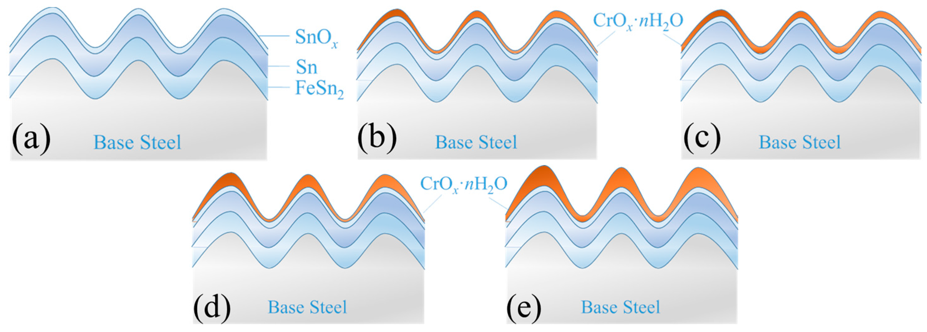
Before the distribution state of the passivation film on the surface of the tinplate is discussed, it is necessary to know the surface structure of the tinplate. It is generally believed that there is a five-layer structure forming the base steel of commercially available tinplate, and as shown in Figure 9, the innermost layer is a tin-iron alloy (FeSn2) layer [34,35]. The next layer is a metal tin layer for which there is no thermal diffusion reaction with the base iron during the reflowing process. The metal tin was oxidized simultaneously at a high temperature when reflowing, and then the tin oxide (SnOx, ()) layer formed on the metal tin [36]. The passivation treatment was carried out after reflowing, and a chromic oxide film then formed on the tin oxide surface; the chemical composition of this film can be expressed as the general formula CrOx·nH2O (mainly Cr2O3, Cr(OH)3, with a small amount of Cr, Cr(VI)) [8,37,38]. The outermost layer is an anti-rust oil film formed from electrostatic oil, which is usually dioctyl sebacate [39,40]. The thickness of the base steel is generally on the millimeter scale; the thickness of the alloy layer and the metal tin layer is on the micron scale; and the thicknesses of all three of the outer layers is on the nanoscale [2,12,13].
The model shown in Figure 9 is the ideal surface structure model of the tinplate, and the composition and structure of tinplate are clearly described. However, the surface of the tinplate may be more complicated. From the above surface roughness data of the tinplate, we know that the surface roughness cannot be neglected in the study of the interface structure of the tinplate. Figure 10 shows a simplified structure model of the tinplate before and after passivated treatment with different processes. Aiming at illustrating the influence of surface roughness on the distribution state of the passivation film on the tinplate, in the model, we only consider the surface roughness instead of considering the surface defects of the tinplate, oil film, and other more complex surface conditions. According to geometrical topography images and SKP scanning maps, the surface structure model of the tinplate samples after passivation are depicted in Figure 10b–e. The chemical passivation film was very thin and uniformly distributed on the tinplate surface. When the tinplate was passivated for a short time via the chemical method, the film that formed on the microscopic bulges was thicker than the film that formed in the microscopic valleys; however, the thickness difference was not very significant, as shown in Figure 10b. When the tinplate was passivated for a longer time, the difference became very small, and so the film was distributed more uniformly on the tinplate surface, as shown in Figure 10c. In general, the electrolytic passivation film was thicker than the chemical passivation film, but its distribution was uneven. When the tinplate was passivated for a short time via the electrolytic method, the film that formed on the microscopic bulges was thicker than that in the microscopic valleys, and the thickness difference was significant, as shown in Figure 10d. When the tinplate was passivated for a longer time, the difference became greater, and the film was distributed more unevenly on the surface, as shown in Figure 10e.
From a theoretical point of view, the reason why the topography and thickness of the chemical passivation and electrolytic passivation films are different is that the film formation mechanisms of the two methods are different. The former is a chemical reaction, whereas the latter is mainly an electrochemical reaction. In the chemical passivation process, SnOx () on the surface is needed to participate in the redox reaction. Thus, it can be imagined that the film attaches to the surface profile of the tinplate to form. In the initial stage of chemical passivation, the surface areas of the valleys do not make contact with the solution immediately, and it requires some time for the solution to reach the valleys. Thus, the reaction time between the microscopic bulges and valleys is different during the same passivation time. Therefore, when the passivation time was short, the areas in the valleys did not make sufficient contact with the solution to participate in the reaction, and thus the film in these areas was thinner. However, because the chemical passivation film was extremely thin in general, the differences in film thickness were not great. When the passivation time was long, the surface areas of the valleys made sufficient contact with the solution, and there was plenty of time to participate in the reaction. Thus, the film thickness further increased, and the result was that the difference between the film thicknesses of the valleys and that of the bulges decreased. Thus, the film was distributed more uniformly on the tinplate surface. Since SnOx is required in the chemical passivation process, after SnOx was oxidized and Cr(VI) was reduced to form the passivation film, it was difficult for the reaction on the passivation film to continue. As a result, it is difficult to further increase the thickness of the film. Therefore, the thickness of the passivation film is relatively thin.
In the electrolytic passivation process, although the chemical redox reactions occurred simultaneously, the process mainly relied on electrochemical action, specifically that Cr(VI) was reduced via cathodic electrolysis to form a Cr(III) oxides passivation film on the tinplate. This reduction reaction did not require the participation of SnOx and could even continue if the film had been covered; thus, the electrolytic passivation film was thicker than the chemical passivation film. However, the uneven thickness distribution of the electrolytic passivation film on the tinplate surface was mainly due to the nonuniform distribution of current density during galvanostatic electrolysis. The chrome electroplating process is characterized by a nonuniform thickness of the coating, and this is caused by the tip effect. In the electrolytic passivation process, the large surface roughness of the tinplate, which is used as the cathode, results in the tip effect occurring at microscopic bulges with high current density. In contrast, the current density at the microscopic valleys was low. For the same electrolysis time, the amount of current that passed through the bulges was high, whereas the amount of current that passed through the valleys was low. In addition, the long process of diffusion and mass transfer in the valleys cause the passivation reaction to be controlled by the diffusion of Cr(VI) ions. The hydrogen evolution reaction competes with the passivation reaction and results in a lower current efficiency. As a consequence, the film was thicker on the bulges but thinner in the valleys, and the difference in the film thickness caused the film distribution to be nonuniform.
4. Discussion
4.1. Performances of the Passivation Film
In the study of a thin film, the thickness is an important quality of the film. However, in the present study, we did not measure the thickness of the passivation film because the film is very thin, and since the thickness distribution of the film on the tinplate surface is uneven, combined with large base roughness, it is difficult to find a test method to accurately detect the thickness of the passivation film. Nevertheless, we found that the distribution state of the film could be deduced by the changes of geometrical topography and work function of the tinplate surface after different processes of passivation treatment in the present study. Therefore, in this study, the reason we investigated the topography and distribution state of the passivation film on the tinplate was to learn more about the information of the invisible film and to use the information to explain some questions or solve some problems. Differences in performances of corrosion and paint adhesion between tinplate samples passivated via chemical and electrolytic methods can be explained in terms of the distribution state of the passivation film on the tinplate surface.
Because the chemical passivation film is thinner than the electrolytic passivation film, corrosive ions can penetrate the former more easily, and thus the tinplate passivated via the chemical method corrodes more easily [1,33]. The tinplate passivated via the electrolytic method does not corrode as easily because of the thicker passivation film [1,33,39]. However, because the distribution state of the film on the surface is not uniform, corrosive ions penetrate the film more easily in microscopic valleys than in microscopic bulges. Once the thin film is destroyed in the corrosion process, it is more likely that micro corrosion cells can develop between valleys (where the film is destroyed) and bulges (which have thicker film) because of the different surface potential between the regions. Then, pitting corrosion is more likely to occur in the microscopic regions where the film is destroyed. With longer passivation time, the corrosion performance of the tinplate improved because of the increase in the film thickness. However, the thickness of the chemical passivation film is limited [33], and thus the corrosion performance can only be improved to a certain extent, after which further passivation does not further improve the corrosion performance. The same is true for the electrolytic passivation film because of poorer uniformity of the film on the surface and because of the destruction of the film caused by hydrogen evolution after a long passivation time. Therefore, if we want to improve the corrosion performance of the tinplate, the passivation time should be prolonged, but it must also be controlled to an appropriate length of time.
Moreover, when considering the paint adhesion of the tinplate, it is believed that the performance of the chemical passivation film is better than that of the electrolytic passivation film [1,4,10]. In addition to the composition and structure of the film, this may also be related to the film thickness and distribution state. Because the electrolytic passivation film is thicker and distributes nonuniformly on the tinplate surface, it may result in the poor performance of paint adhesion because of the nonuniform distribution of adhesive forces. With longer passivation time, the performance of the electrolytic passivation film becomes worse because of the increase in the thickness of the film and because of the degradation of the uniformity of the film distribution. Therefore, if we want to obtain a tinplate with good paint adhesion, chemical passivation treatment for an appropriate length of time should be used. On the contrary, if electrolytic passivation must be used, the time should be controlled to a short length of time.
4.2. Chemical Analysis of the Passivation Film
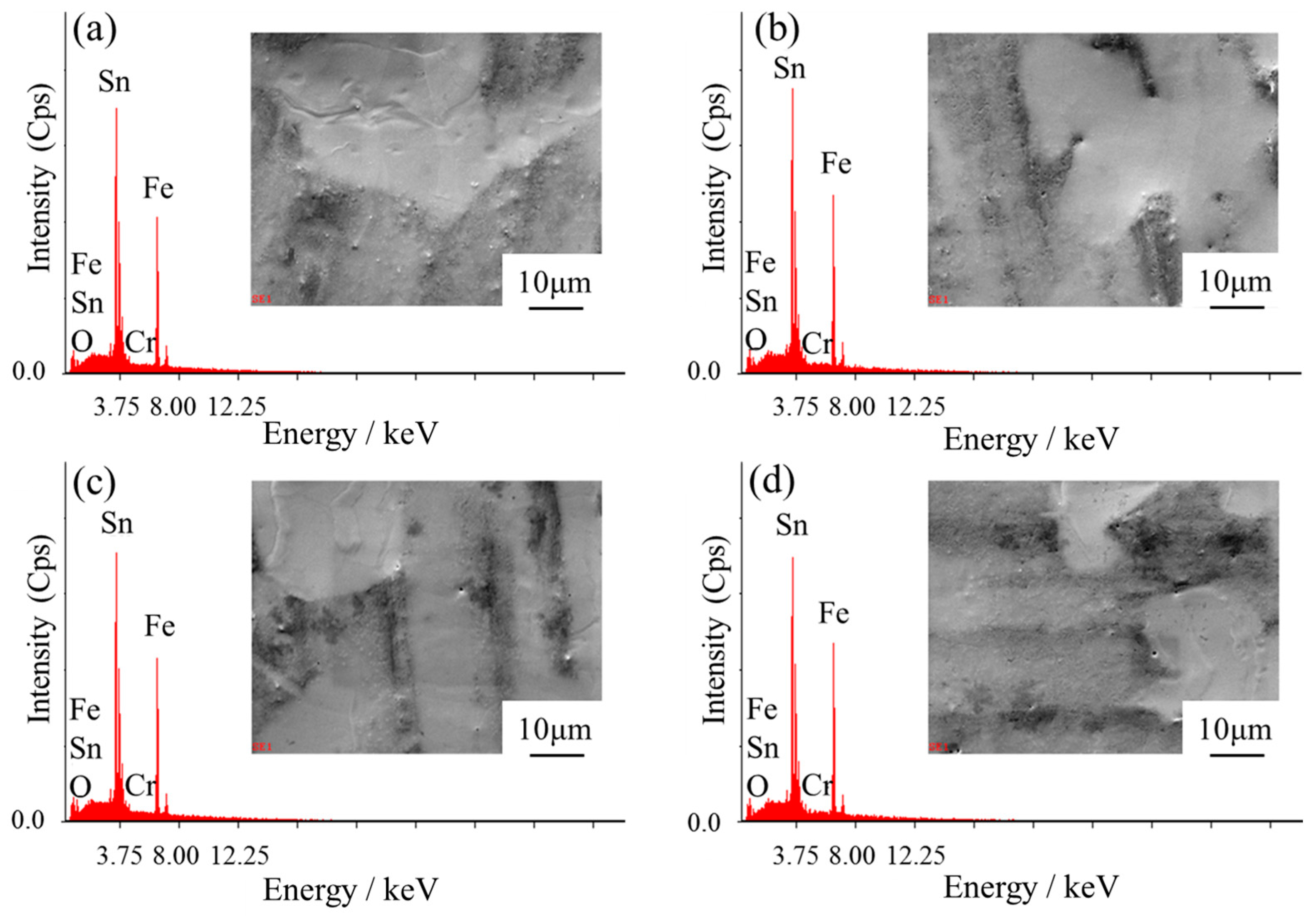
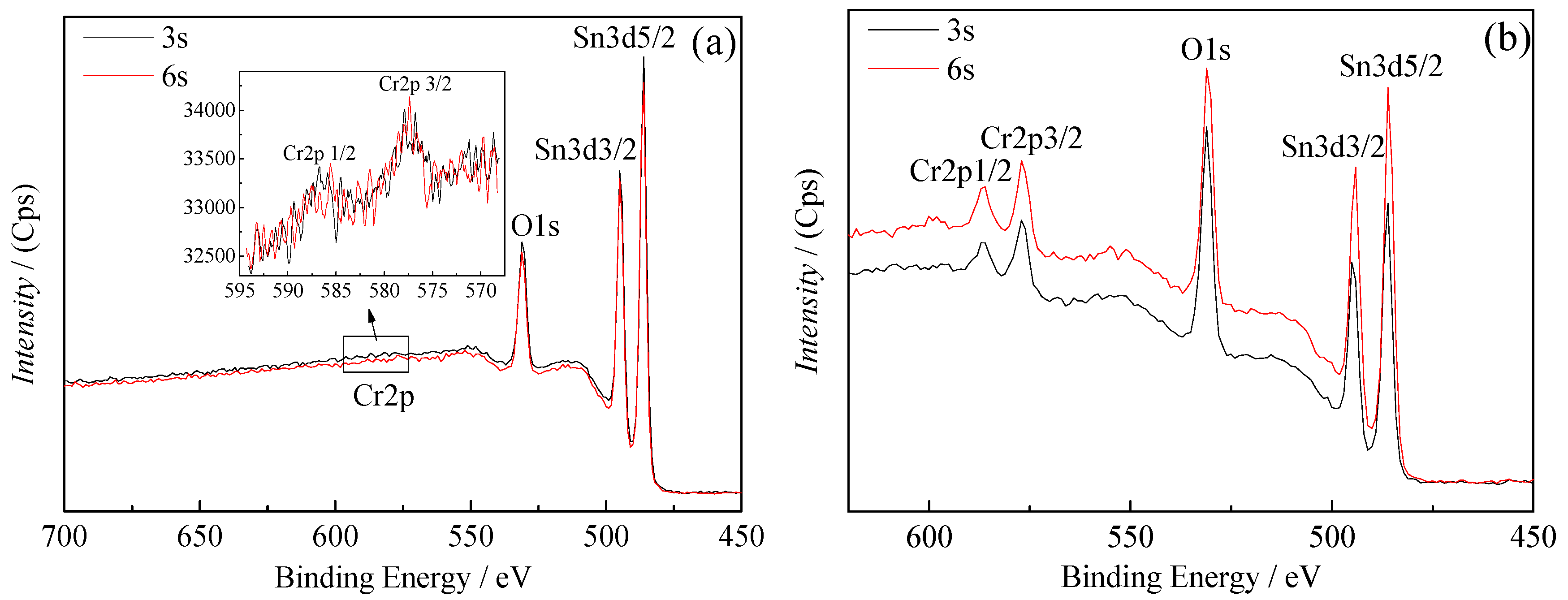
In our previous study, we talked about the differences in distribution state that can affect the performances of the passivation film on tinplate. However, the factors that affect the performance of the passivation film are more complicated. The fundamental factors that affect the performance of the passivation film depend on the chemical nature of the film. Surface elements of the tinplate samples were detected by Energy Dispersive X-ray Spectroscopy (EDX) in the corresponding SEM image area, as shown in Figure 11. The results indicated that the elements chromium, oxygen, tin, and iron were detected on the tinplate surface. Atomic percentages of the elements on the tinplate surface treated with different passivation processes are listed in Table 3.
As listed in Table 3, chromium content on the tinplate surface treated with chemical passivation was lower than that on the tinplate surface treated with electrolytic passivation. With longer passivation time, whether chemical or electrolytic passivation, the chromium content increased. Considering the detection depth of the EDX, the XPS (X-ray photoelectron spectroscopy) test with a detection depth within 10 nm was more suitable for detecting the thin film. Surface elements of the tinplate samples were then detected by XPS, as shown in Figure 12. The peaks were found and compared with the standard database using CasaXPS software (Version 2.3.16), as listed in Table 4. The results indicated that the elements chromium, oxygen, and tin were detected on the tinplate surface. Atomic percentages of the elements on the tinplate surface were calculated utilizing CasaXPS and are listed in Table 5. The same results found through the EDX test can be drawn from Table 5. Combined with the performances of the tinplate discussed above, it can be inferred that low chromium content on the tinplate surface may result in poor corrosion performance and good paint adhesion, while high chromium content indicates the opposite.
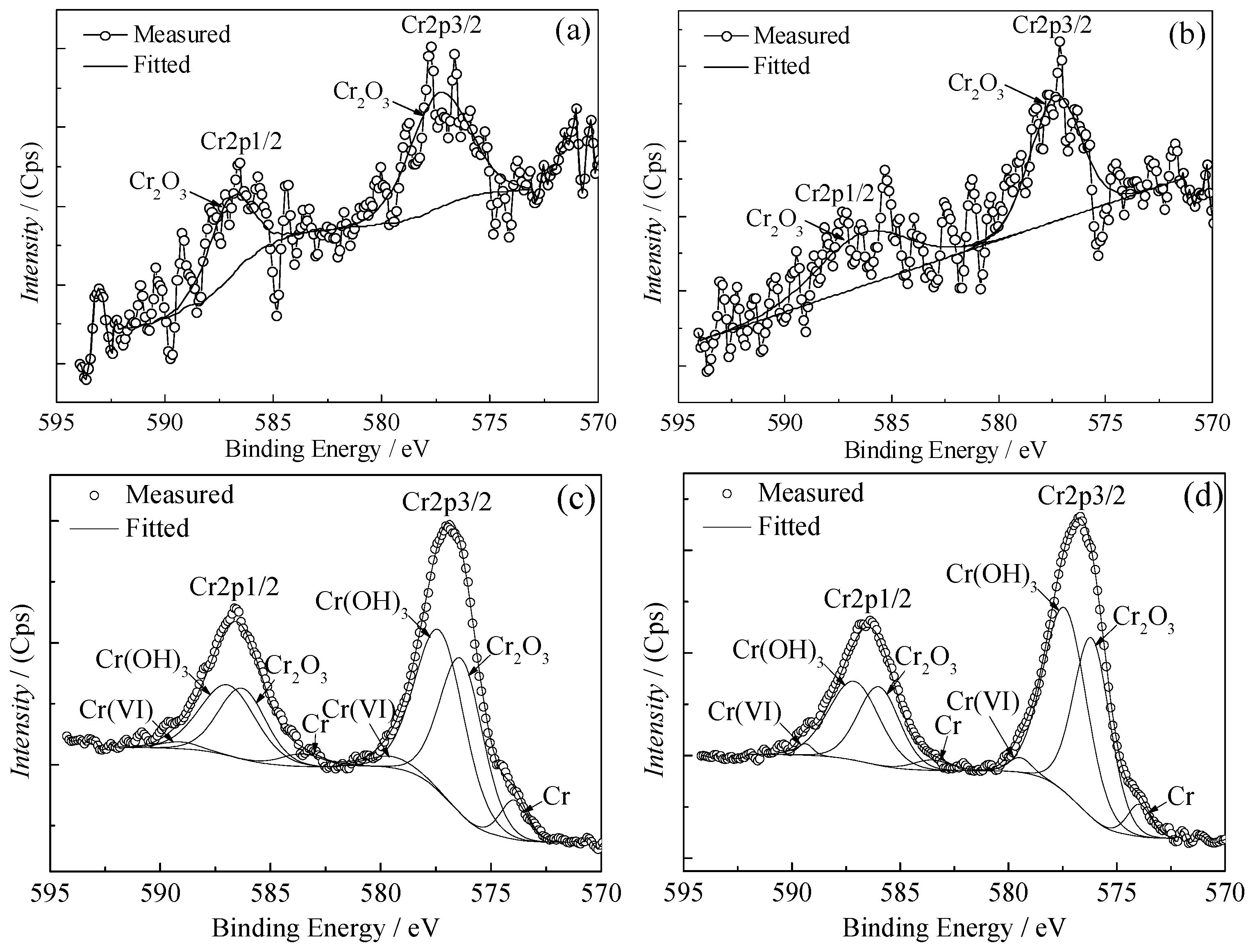
The composition of the passivation film was analyzed by fitting the Cr2p peaks using CasaXPS. The measured and fitted Cr2p peaks are shown in Figure 13. The binding energy values of the fitting peaks are listed in Table 6 and the chemical composition of the film was obtained by referring to the relevant literature [8,33,41,42,43] and comparing the binding energy values. The chemical passivation film is only composed of Cr2O3. The electrolytic passivation film is mainly composed of Cr(OH)3 and Cr2O3; also, there are a small amount of metal chromium, Cr, and hexavalent compounds, Cr(VI). The atomic percentage of the different components (Table 7) showed that the relative content of Cr(OH)3 in the film increased with longer electrolytic passivation time. Combined with the performances of the tinplate discussed above, it can be inferred that a high relative content of Cr(OH)3 may result in good corrosion performance and poor paint adhesion, while a low relative content of Cr(OH)3 results in the opposite.
5. Conclusions
In the present study, we observed the topography of the nanoscale passivation film on tinplate samples with high surface roughness, and found the difference in the distribution state of the films prepared with different passivated processes using a profilometer and SKPM. The results suggest that the chemical passivation film distributes more uniformly on an uneven tinplate surface than the electrolytic passivation film. For electrolytic passivation, the film is much thicker on the microscopic bulges than that in the microscopic valleys, and the thickness difference increased with longer passivation time. In contrast, the distribution uniformity of the film was further improved with longer passivation time for the chemical passivation film.
Acknowledgments
This work has been supported by the National Natural Science Foundation of China (51475119). The authors would also like to acknowledge Baoshan Iron & Steel Co., Ltd. (Baosteel) for its financial support and materials supply for this work, as well as all of the involved coworkers.
Author Contributions
Minghao Wang and Ning Li conceived and designed the experiments; Minghao Wang and Ziyu Wang performed the experiments; Minghao Wang, Deyu Li, and Ning Li analyzed the data; Deyu Li contributed reagents and materials, Ziyu Wang contributed analysis tools; Minghao Wang wrote the paper.
Conflicts of Interest
The authors declare no conflict of interest.
References
- Biermann, M.C.; Sandenbergh, R.F.; von Moltke, T.v.S. Characteristics and lacquer adhesion on dip and CDC chromium passivated tinplate. Corros. Sci. 2006, 48, 2925–2936. [Google Scholar] [CrossRef]
- Rauch, S.E.; Steinbicker, R.N. A Study of surface chromium on tinplate. J. Electrochem. Soc. 1973, 120, 735–738. [Google Scholar] [CrossRef]
- Britton, S.C. Electrochemical assessment of chromium in passivation films on tinplate. Brit. Corros. J. 1965, 1, 91–97. [Google Scholar] [CrossRef]
- Bastidas, J.M.; Cabañes, J.M.; Catalá, R. Effect of passivation treatment and storing on adhesion and protective properties of lacquered tinplate cans. J. Coat. Technol. 1997, 69, 67–71. [Google Scholar] [CrossRef]
- Álvarez, D.; Collazo, A.; Nóvoa, X.R.; Pérez, C. The anticorrosive properties of sol-gel films doped with hydrotalcite nanoparticles applied on tinplate. Electrochim. Acta 2014, 131, 137–147. [Google Scholar] [CrossRef]
- Álvarez, D.; Collazo, A.; Nóvoa, X.R.; Pérez, C. Electrochemical behavior of organic/inorganic films applied on tinplate in different aggressive media. Prog. Org. Coat. 2014, 77, 2066–2075. [Google Scholar] [CrossRef]
- Huang, X.; Li, N. Structural characterization and properties of lanthanum film as chromate replacement for tinplate. Appl. Surf. Sci. 2007, 254, 1463–1470. [Google Scholar] [CrossRef]
- Chen, S.; Xie, L.; Xue, F. X-ray photoelectron spectroscopy investigation of commercial passivated tinplate surface layer. Appl. Surf. Sci. 2013, 276, 454–457. [Google Scholar] [CrossRef]
- Sun, J.; Qi, G.C.; Tan, Y.; An, C.Q. Characterization of chromate conversion film on tinplate substrate by XPS and electrochemistry methods. Surf. Interface Anal. 2009, 41, 449–452. [Google Scholar] [CrossRef]
- Helwig, E.J. Modifying the CDC passivation treatment to enhance adhesion performance of epoxy-phenolic lacquers on tinplate. In Proceedings of the Sixth International Tinplate Conference, London, UK, 16–20 September 1996. [Google Scholar]
- Cao, C.; Cheung, M.M.S.; Chan, B.Y.B. Modelling of interaction between corrosion-induced concrete cover crack and steel corrosion rate. Corros. Sci. 2013, 69, 97–109. [Google Scholar] [CrossRef]
- Arenas, M.A.; Conde, A.; Damborenea, J.J. Cerium: A suitable green corrosion inhibitor for tinplate. Corros. Sci. 2002, 44, 511–520. [Google Scholar] [CrossRef]
- Albu-Yaron, A.; Smith, D.A. Some transmission electron microscope observations of the structure and composition of passivation films on tinplate. Brit. Corros. J. 1979, 14, 133–136. [Google Scholar] [CrossRef]
- Hollaender, J. Influence of steel roughness on internal and external corrosion of tinplate cans. Packag. Technol. Sci. 2010, 2, 147–154. [Google Scholar] [CrossRef]
- Ramamurthy, S.; Walzak, T.L.; Lu, S.F.; Lipson, T.C.; McIntyre, N.S. Study of tinplate structure using imaging secondary ion spectrometry. Surf. Interface Anal. 1991, 17, 834–841. [Google Scholar] [CrossRef]
- Lu, S.F.; Mount, G.R.; McIntyre, N.S.; Fenster, A. Use of image depth profiling SIMS for the study of tinplate corrosion. Surf. Interface Anal. 1994, 21, 177–183. [Google Scholar] [CrossRef]
- Caber, P.J. Interferometric profiler for rough surfaces. Appl. Opt. 1993, 32, 3438–3441. [Google Scholar] [CrossRef] [PubMed]
- Brinker, W.; Yilmaz, S.; Wirges, W.; Bauer, S.; Gerhard-Multhaupt, R. Phase-shift interference microscope for the investigation of dipole-orientation distributions. Opt. Lett. 1995, 20, 816–818. [Google Scholar] [CrossRef] [PubMed]
- Lee, C.; Mong, H.; Lin, W. Noninterferometric wide-field optical profilometry with nanometer depth resolution. Opt. Lett. 2002, 27, 1773–1775. [Google Scholar] [CrossRef] [PubMed]
- Joniot, S.B.; Gregoire, G.L.; Auther, A.M.; Roques, Y.M. Three-dimensional optical profilometry analysis of surface states obtained after finishing sequences for three composite resins. Oper. Dent. 2000, 25, 311–315. [Google Scholar] [PubMed]
- Sandoz, P.; Tribillon, G.; Perrin, H. High-resolution profilometry by using phase calculation algorithms for spectroscopic analysis of white-light interferograms. J. Mod. Opt. 1996, 43, 701–708. [Google Scholar] [CrossRef]
- Uebel, M.; Vimalanandan, A.; Laaboudi, A.; Evers, S.; Stratmann, M.; Diesing, D.; Rohwerder, M. Fabrication of robust reference tips and reference electrodes for Kelvin probe applications in changing atmospheres. Langmuir 2017, 33, 10807–10817. [Google Scholar] [CrossRef] [PubMed]
- Baikie, I.D.; Estrup, P.J. Low cost PC based scanning Kelvin probe. Rev. Sci. Instrum. 1998, 69, 3902–3907. [Google Scholar] [CrossRef]
- McMurray, H.N.; Williams, G. Probe diameter and probe–specimen distance dependence in the lateral resolution of a scanning Kelvin probe. J. Appl. Phys. 2002, 91, 1673–1679. [Google Scholar] [CrossRef]
- Ebrahimi, G.; Neshati, J.; Rezaei, F. An investigation on the effect of H3PO4 and HCl-doped polyaniline nanoparticles on corrosion protection of carbon steel by means of scanning kelvin probe. Prog. Org. Coat. 2017, 105, 1–8. [Google Scholar] [CrossRef]
- Benaioun, N.E.; Maafa, I.; Florentin, A.; Denys, E.; Hakiki, N.E.; Moulayat, N.; Bubendorff, J.L. Time dependence of the natural passivation process on AISI 304 in an alkaline medium: Atomic Force Microscopy and Scanning Kelvin Probe Force Microscopy as additional tools to Electrochemical Impedance Spectroscopy. Appl. Surf. Sci. 2018, 436, 646–652. [Google Scholar] [CrossRef]
- Leng, A.; Streckel, H.; Stratmann, M. The delamination of polymeric coatings from steel. Part 1: Calibration of the Kelvinprobe and basic delamination mechanism. Corros. Sci. 1998, 41, 547–578. [Google Scholar] [CrossRef]
- Bard, A.J.; Faulkner, L.R. Electrochemical Methods: Fundamentals and Applications, 2nd ed.; John Wiley & Sons, Inc.: New York, NY, USA, 2001; pp. 59–63. [Google Scholar]
- Rohwerder, M.; Turcu, F. High-resolution Kelvin probe microscopy in corrosion science: Scanning Kelvin probe force microscopy (SKPFM) versus classical scanning Kelvin probe (SKP). Electrochim. Acta 2007, 53, 290–299. [Google Scholar] [CrossRef]
- Melitz, W.; Shen, J.; Kummel, A.C.; Lee, S. Kelvin probe force microscopy and its application. Surf. Sci. Rep. 2011, 66, 1–27. [Google Scholar] [CrossRef]
- Skriver, H.L.; Rosengaard, N.M. Surface energy and work function of elemental metals. Phys. Rev. B Cond. Mat. 1992, 46, 7157–7168. [Google Scholar] [CrossRef] [Green Version]
- Lü, J.; Delamarche, E.; Eng, L.; Bennewitz, R.; Meyer, E.; Güntherodt, H. Kelvin probe force microscopy on surfaces: Investigation of the surface potential of self-assembled monolayers on gold. Langmuir 1999, 15, 8184–8188. [Google Scholar] [CrossRef]
- Biermann, M.C. A critical assessment of the Current Understanding of Chromium Passivation Treatments on Tinplate. Ph.D. Thesis, University of Pretoria, Pretoria, South Africa, 2005. [Google Scholar]
- Kunst, S.R.; Beltrami, L.V.R.; Cardoso, H.R.P.; Veja, M.R.O.; Baldin, E.K.K.; Menezes, T.L.; Malfatti, C.D.F. Effect of curing temperature and architectural (monolayer and bilayer) of hybrid films modified with polyethylene glycol for the corrosion protection on tinplate. Mater. Res. 2014, 17, 1071–1081. [Google Scholar] [CrossRef]
- Biber, H.E. The kinetics of growth of FeSn2 layers on tinplate. J. Electrochem. Soc. 1966, 113, 362–365. [Google Scholar] [CrossRef]
- Britton, S.C.; Sherlock, J.C. Examination of oxides on tin surfaces by cathodic reduction. Brit. Corros. J. 1974, 9, 96–102. [Google Scholar] [CrossRef]
- Zumelzu, E.; Cabezas, C. Observations on the influence of microstructure on electrolytic tinplate corrosion. Mater. Charact. 1995, 34, 143–148. [Google Scholar] [CrossRef]
- Becker, J.J. Surface chromium on chromate treated tin plate. J. Electrochem. Soc. 1970, 117, 1211–1215. [Google Scholar] [CrossRef]
- Martins, J.I. Corrosion problems in tinplate cans for storing contact glues for shoes. Eng. Fail. Anal. 2012, 26, 258–265. [Google Scholar] [CrossRef]
- Zumelzu, E.; Rull, F. Evaluation of adherence and performance of epoxyphenolic coatings on electrolytic tinplates. Sci. Eng. Compos. Mater. 2002, 10, 345–352. [Google Scholar] [CrossRef]
- Desimoni, E.; Malitesta, C.; Zambonin, P.G. An X-ray photoelectron spectroscopic study of some chromium–oxygen systems. Surf. Interface Anal. 1988, 13, 173–179. [Google Scholar] [CrossRef]
- Petkov, K.; Krastev, V.; Marinova, T. XPS analysis of thin chromium films. Surf. Interface Anal. 1992, 18, 487–490. [Google Scholar] [CrossRef]
- Yang, W.P.; Costa, D.; Marcus, P. Chemical composition, chemical states, and resistance to localized corrosion of passive films on an Fe-17% Cr alloy. J. Electrochem. Soc. 1994, 141, 111–116. [Google Scholar] [CrossRef]
Figure 1.
SEM images (2000×) of tinplate treated with (a) reflowing before passivation, (b) chemical passivation, and (c) electrolytic passivation.
Figure 1.
SEM images (2000×) of tinplate treated with (a) reflowing before passivation, (b) chemical passivation, and (c) electrolytic passivation.

Figure 2.
SEM images (5000×) of tinplate treated with (a) reflowing before passivation, (b) chemical passivation, and (c) electrolytic passivation.
Figure 2.
SEM images (5000×) of tinplate treated with (a) reflowing before passivation, (b) chemical passivation, and (c) electrolytic passivation.

Figure 3.
Geometrical topography of tinplate treated with (a) reflowing before passivation, (b) chemical passivation, and (c) electrolytic passivation.
Figure 3.
Geometrical topography of tinplate treated with (a) reflowing before passivation, (b) chemical passivation, and (c) electrolytic passivation.
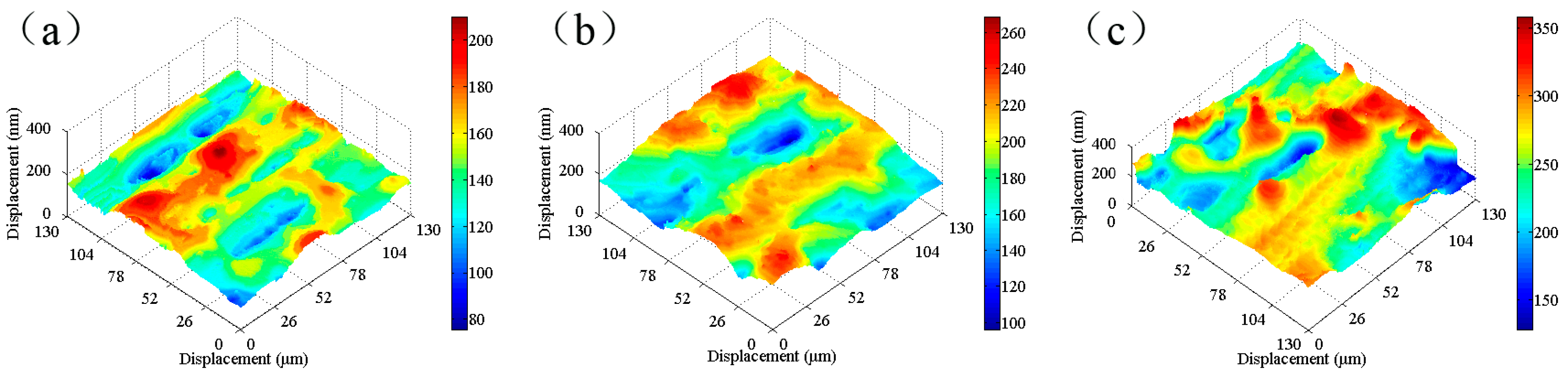
Figure 4.
(a) Appearance photo and (b,c) SEM images of the topography of the bright tin plating.
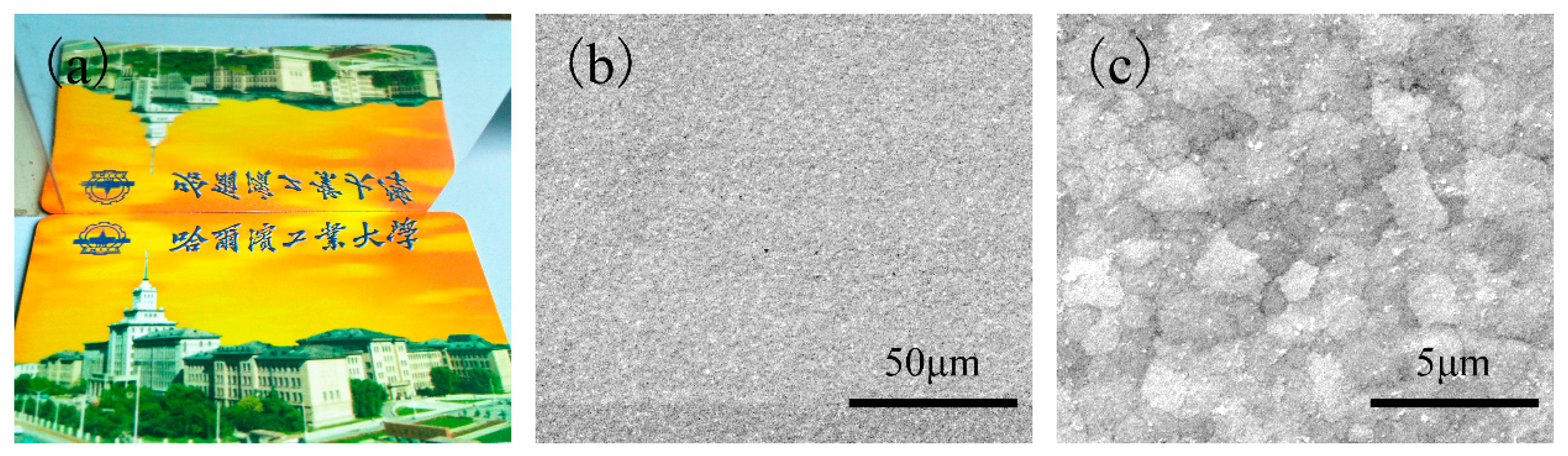
Figure 5.
SEM images of bright tin plating treated with (a,b) chemical passivation and (c,d) electrolytic passivation.
Figure 5.
SEM images of bright tin plating treated with (a,b) chemical passivation and (c,d) electrolytic passivation.

Figure 6.
Geometrical topography images of (a) bright tin plating; (b,c) bright tin plating treated with chemical passivation for 3 s and 6 s, respectively; and (d,e) bright tin plating treated with electrolytic passivation for 3 s and 6 s, respectively.
Figure 6.
Geometrical topography images of (a) bright tin plating; (b,c) bright tin plating treated with chemical passivation for 3 s and 6 s, respectively; and (d,e) bright tin plating treated with electrolytic passivation for 3 s and 6 s, respectively.

Figure 7.
Schematic diagram of the scanning Kelvin probe microscope in (a) noncontact mode, (b) contact mode, and (c) test mode.
Figure 7.
Schematic diagram of the scanning Kelvin probe microscope in (a) noncontact mode, (b) contact mode, and (c) test mode.
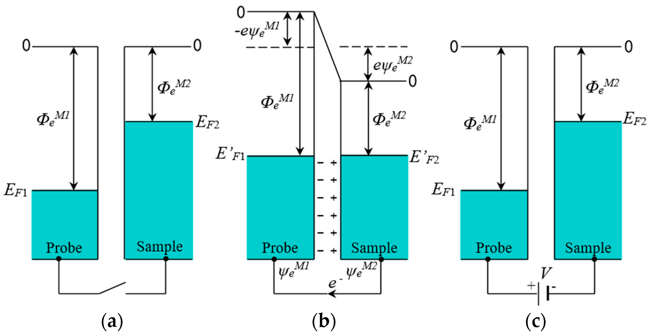
Figure 8.
Work function maps of the tinplate samples treated with (a) reflowing before passivation; (b,c) chemical passivation for 3 s and 6 s, respectively; and (d,e) electrolytic passivation for 3 s and 6 s, respectively.
Figure 8.
Work function maps of the tinplate samples treated with (a) reflowing before passivation; (b,c) chemical passivation for 3 s and 6 s, respectively; and (d,e) electrolytic passivation for 3 s and 6 s, respectively.
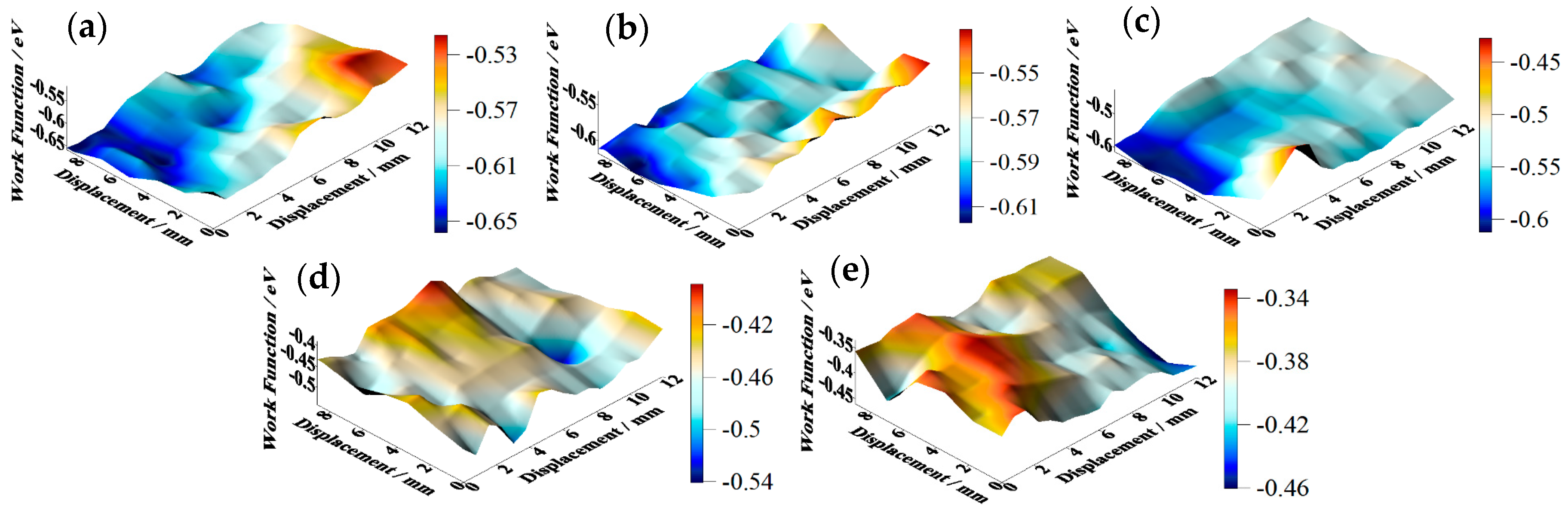
Figure 9.
Schematic diagram of the ideal structure model of the tinplate surface and the interface.
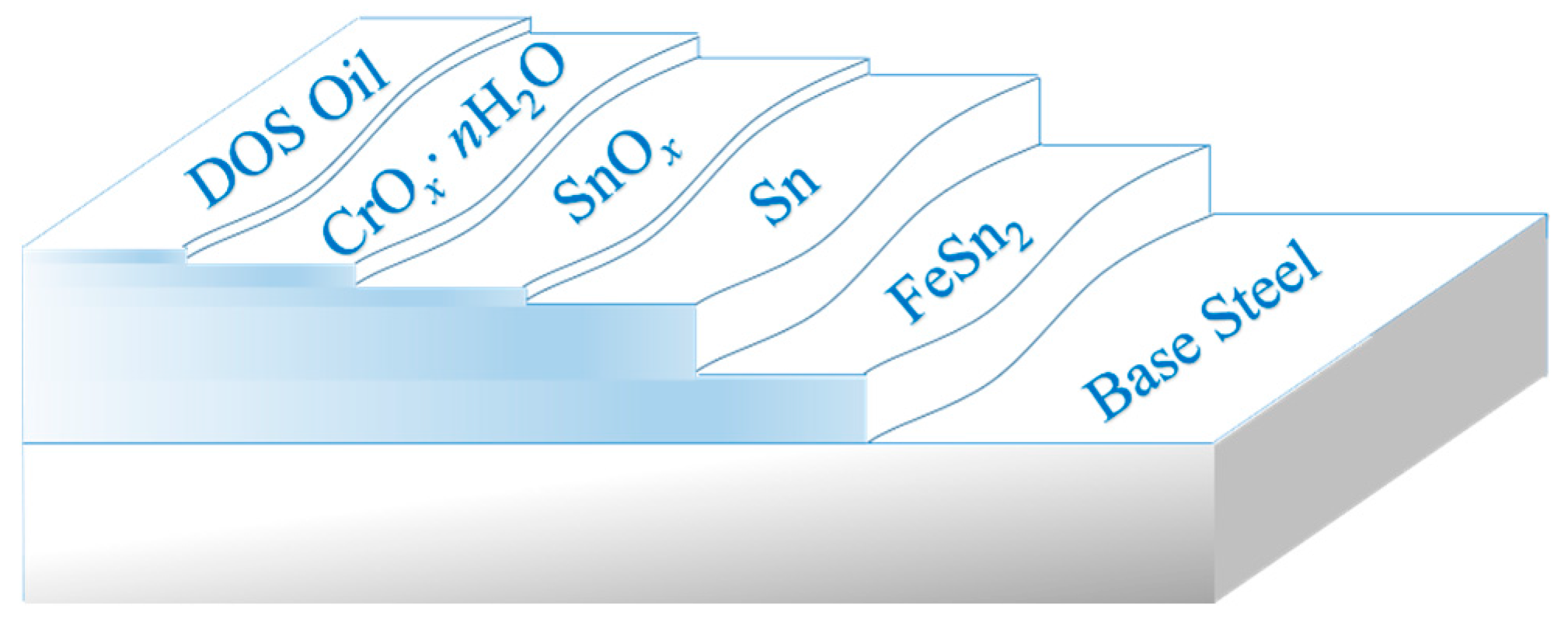
Figure 10.
Schematic diagram of structure models of the tinplate treated with (a) reflowing before passivation; (b,c) chemical passivation for 3 s and 6 s, respectively; and (d,e) electrolytic passivation for 3 s and 6 s, respectively.
Figure 10.
Schematic diagram of structure models of the tinplate treated with (a) reflowing before passivation; (b,c) chemical passivation for 3 s and 6 s, respectively; and (d,e) electrolytic passivation for 3 s and 6 s, respectively.

Figure 11.
Energy Dispersive X-ray Spectroscopy (EDX) survey spectrogram of the tinplate surface treated with (a,b) chemical passivation for 3 s and 6 s, respectively, and (c,d) electrolytic passivation for 3 s and 6 s, respectively.
Figure 11.
Energy Dispersive X-ray Spectroscopy (EDX) survey spectrogram of the tinplate surface treated with (a,b) chemical passivation for 3 s and 6 s, respectively, and (c,d) electrolytic passivation for 3 s and 6 s, respectively.

Figure 12.
XPS survey spectrogram of the tinplate surface treated with (a) chemical passivation for different times and (b) electrolytic passivation for different times.
Figure 12.
XPS survey spectrogram of the tinplate surface treated with (a) chemical passivation for different times and (b) electrolytic passivation for different times.

Figure 13.
Cr2p peaks measured by XPS and fitted curves of Cr2p peaks for the passivation films obtained via (a,b) chemical passivation for 3 s and 6 s, respectively, and (c,d) electrolytic passivation for 3 s and 6 s, respectively.
Figure 13.
Cr2p peaks measured by XPS and fitted curves of Cr2p peaks for the passivation films obtained via (a,b) chemical passivation for 3 s and 6 s, respectively, and (c,d) electrolytic passivation for 3 s and 6 s, respectively.

Table 1.
Surface roughness (Ra, nm) values of tinplate samples treated with different processes.
| Tinplate Sample | Ra (1) | Ra (2) | Ra (3) | Ra (4) | Ra (5) | Ra (6) | Ra (7) | Standard Deviation | |
|---|---|---|---|---|---|---|---|---|---|
| Reflowing | 127.34 | 115.95 | 131.47 | 180.84 | 137.21 | 164.21 | 136.59 | 141.94 | 22.58 |
| Chemical passivation | 135.59 | 151.30 | 119.55 | 167.68 | 153.73 | 118.91 | 154.86 | 143.09 | 18.79 |
| Electrolytic passivation | 213.09 | 223.68 | 241.15 | 269.46 | 205.95 | 216.66 | 228.5 | 228.36 | 21.40 |
Table 2.
Surface roughness (Ra, nm) of bright tin plating treated with different processes.
| Tinplate Sample | Ra (1) | Ra (2) | Ra (3) | Ra (4) | Ra (5) | Ra (6) | Ra (7) | Standard Deviation | |
|---|---|---|---|---|---|---|---|---|---|
| Bright tin plating | 22.12 | 24.19 | 20.63 | 22.05 | 19.92 | 23.04 | 24.95 | 22.41 | 1.81 |
| Chemical passivation for 3 s | 27.43 | 26.89 | 25.01 | 24.32 | 29.69 | 28.62 | 25.49 | 26.78 | 1.96 |
| Chemical passivation for 6 s | 23.94 | 24.66 | 26.88 | 27.53 | 24.19 | 22.91 | 22.06 | 24.60 | 1.99 |
| Electrolytic passivation for 3 s | 35.84 | 40.29 | 37.67 | 42.92 | 34.38 | 36.61 | 38.91 | 38.09 | 2.89 |
| Electrolytic passivation for 6 s | 41.74 | 43.39 | 50.99 | 45.62 | 47.69 | 49.76 | 42.26 | 45.92 | 3.67 |
Table 3.
Atomic percentage (at.%) of the elements on the tinplate surface treated with different passivation processes.
Table 3.
Atomic percentage (at.%) of the elements on the tinplate surface treated with different passivation processes.
| Tinplate Sample | Cr K | O K | Sn L | |
|---|---|---|---|---|
| Chemical passivation | 3 s | 0.36 | 12.21 | 87.43 |
| 6 s | 0.57 | 14.04 | 85.39 | |
| Electrolytic passivation | 3 s | 0.87 | 14.29 | 84.84 |
| 6 s | 1.08 | 13.92 | 84.99 | |
Table 4.
Binding energy (eV) of the XPS peaks by surveying the tinplate surface treated with different passivation processes.
Table 4.
Binding energy (eV) of the XPS peaks by surveying the tinplate surface treated with different passivation processes.
| Tinplate Sample | Cr2p1/2 | Cr2p3/2 | O1s | Sn3d3/2 | Sn3d5/2 | |
|---|---|---|---|---|---|---|
| Chemical passivation | 3 s | 587.00 | 577.33 | 530.94 | 495.01 | 485.94 |
| 6 s | 586.35 | 577.12 | 530.86 | 494.88 | 485.86 | |
| Electrolytic passivation | 3 s | 586.97 | 576.96 | 530.94 | 494.66 | 485.94 |
| 6 s | 586.51 | 576.89 | 530.89 | 494.32 | 485.89 | |
Table 5.
Atomic percentage (at.%) of the elements on the tinplate surface treated with different passivation processes.
Table 5.
Atomic percentage (at.%) of the elements on the tinplate surface treated with different passivation processes.
| Tinplate Sample | Cr2p | O1s | Sn3d | |
|---|---|---|---|---|
| Chemical passivation | 3 s | 0.69 | 66.13 | 33.18 |
| 6 s | 1.55 | 66.01 | 32.44 | |
| Electrolytic passivation | 3 s | 11.50 | 74.25 | 14.25 |
| 6 s | 13.68 | 70.43 | 15.89 | |
Table 6.
Binding energy (eV) of the fitting Cr2p peaks and composition of the passivation films obtained through different processes.
Table 6.
Binding energy (eV) of the fitting Cr2p peaks and composition of the passivation films obtained through different processes.
| Tinplate Sample | Cr(OH)3 | Cr2O3 | Cr | Cr(VI) | |
|---|---|---|---|---|---|
| Chemical passivation | 3 s | – | 577.3, 586.0 | – | – |
| 6 s | – | 577.3, 586.5 | – | – | |
| Electrolytic passivation | 3 s | 577.3, 586.9 | 576.3, 586.3 | 574.0, 583.5 | 579.5, 589.1 |
| 6 s | 577.4, 587.1 | 576.2, 586.0 | 574.0, 583.5 | 579.5, 589.4 | |
Table 7.
Atomic percentage (at.%) of the composition of the passivation films obtained through different processes.
Table 7.
Atomic percentage (at.%) of the composition of the passivation films obtained through different processes.
| Tinplate Sample | Cr(OH)3 | Cr2O3 | Cr | Cr(VI) | |
|---|---|---|---|---|---|
| Chemical passivation | 3 s | – | 100.00 | – | – |
| 6 s | – | 100.00 | – | – | |
| Electrolytic passivation | 3 s | 48.82 | 41.44 | 6.55 | 3.18 |
| 6 s | 51.03 | 41.89 | 4.88 | 2.20 | |
© 2018 by the authors. Licensee MDPI, Basel, Switzerland. This article is an open access article distributed under the terms and conditions of the Creative Commons Attribution (CC BY) license (http://creativecommons.org/licenses/by/4.0/).
Share and Cite
MDPI and ACS Style
Wang, M.; Wang, Z.; Li, D.; Li, N. Study of Topography and Distribution State of the Nanoscale Passivation Film on a Rough Tinplate Surface. Coatings 2018, 8, 94. https://doi.org/10.3390/coatings8030094
AMA Style
Wang M, Wang Z, Li D, Li N. Study of Topography and Distribution State of the Nanoscale Passivation Film on a Rough Tinplate Surface. Coatings. 2018; 8(3):94. https://doi.org/10.3390/coatings8030094
Chicago/Turabian StyleWang, Minghao, Ziyu Wang, Deyu Li, and Ning Li. 2018. "Study of Topography and Distribution State of the Nanoscale Passivation Film on a Rough Tinplate Surface" Coatings 8, no. 3: 94. https://doi.org/10.3390/coatings8030094
Note that from the first issue of 2016, this journal uses article numbers instead of page numbers. See further details here.