Article

The Influence of Oxygen Flow Ratio on the Optoelectronic Properties of p-Type Ni1−xO Films Deposited by Ion Beam Assisted Sputtering

1
School of Space Science and Physics, Shandong University at Weihai, 180 Wenhuaxi Road, Weihai 264209, China
2
Department of Materials Engineering and Center for Thin Film Technologies and Applications, Ming Chi University of Technology, Taipei 243, Taiwan
3
Department of Electronic Engineering, Chang Gung University, Taoyuan 333, Taiwan
4
Institute of Materials Science and Engineering, National Taiwan University, Taipei 106, Taiwan
5
Institute of Materials Science and Engineering, Ocean University of China, 238 Songling Road, Qingdao 266100, China
*
Author to whom correspondence should be addressed.
Coatings 2018, 8(5), 168; https://doi.org/10.3390/coatings8050168
Submission received: 26 March 2018 / Revised: 20 April 2018 / Accepted: 25 April 2018 / Published: 30 April 2018

Abstract

:
In this work, p-type non-stoichiometric Ni1−xO thin films were deposited by oxygen ion beam assisted RF sputtering on glass substrates. The influence of the oxygen flow ratio (0–100%) on the films’ optoelectronic properties was investigated. In our experimental conditions, all the films are crystallized in the cubic NiO phase. However, their crystallinity and mean grain size decreases with increasing oxygen flow ratios. Meanwhile, the films’ conductivity improves from 9.1 to 25.4 S·cm−1. This is due to the fact that the nickel vacancies along with hole carriers can be introduced into NiO films when they are deposited under higher oxygen flow ratio conditions. Thus, the O-rich environment is beneficial in enhancing the films’ carrier concentrations. In addition, with an increasing oxygen flow ratio, the film’s transmittance degrades. The direct optical band gap of Ni1−xO films declines slightly from 3.99 to 3.95 eV, with the oxygen flow ratio increasing from 0% to 100%.

Graphical Abstract

1. Introduction

Transparent conductive oxides (TCOs) have aroused people’s attention due to their potential applications in the fields of flat panel displays, light emitting diodes, solar cells, smart windows, and photocatalysts [1,2,3,4,5]. They possess a wide band gap, generally greater than 3.0 eV, and so are transparent in the visible light spectrum. To date, the traditional TCOs, including In2O3, ZnO, and SnO2, have been widely employed in commercial applications [6,7,8,9]. All of them present good n-type conductivity. However, producing p-type TCOs with high resistivity and low transparency has proven to be more elusive in contrast with n-type TCOs [10,11,12]. The slow development of p-type TCOs has limited the implementation of the transparent p–n junctions, which is of interest for use in photovoltaics and invisible electronic devices.
Generally, due to the top valence band of TCOs being predominantly composed of O 2p states, it is difficult to introduce free holes into a valence band of oxides owing to their strong localization by O 2p [13,14]. Thus, most TCOs are intrinsic n-type semiconductors. Currently, the extensively studied intrinsic p-type TCOs are mainly focused on Cu-based oxides and Ni-based oxides [15,16,17,18]. In particular, NiO is considered an attractive candidate due to its wide band gap above 3.6 eV, intrinsic p-type conductivity, abundant availability, chemical stability, non-toxicity, low-cost, the fact that its easily producible, etc. [19,20,21]. To date, NiO has been widely studied in various domains, such as photoanodes [22], electrochromic materials [23], gas sensors [24], and photoelectrochemical cells [25,26]. The reported optoelectronic properties of NiO films are compared in Table 1. Recently, nickel vacancies (VNi″) were proven to play an important role in NiO films’ electrical properties. These can be spontaneously formed under oxygen-rich conditions [27,28]. Holes can be generated from nickel vacancies and are responsible for the films’ p-type conductivity. Thus, the dilemma of how to introduce nickel vacancies into NiO films has become a hot topic for researchers.
In our previous work, oxygen ion beam assisted RF sputtering was employed to deposit NiO thin films in pure Ar conditions [32]. The films’ electrical properties are significantly improved compared with the films prepared by RF sputtering without oxygen ion beam assistance. As mentioned above, an oxygen-rich deposition environment is beneficial for the formation of Ni vacancies and holes. Thus, in the current work, oxygen flow is added into the sputtering system in order to further improve the films’ electrical conductivity. The influence of the oxygen flow ratio (fO2) on the films’ optoelectronic properties is studied here.

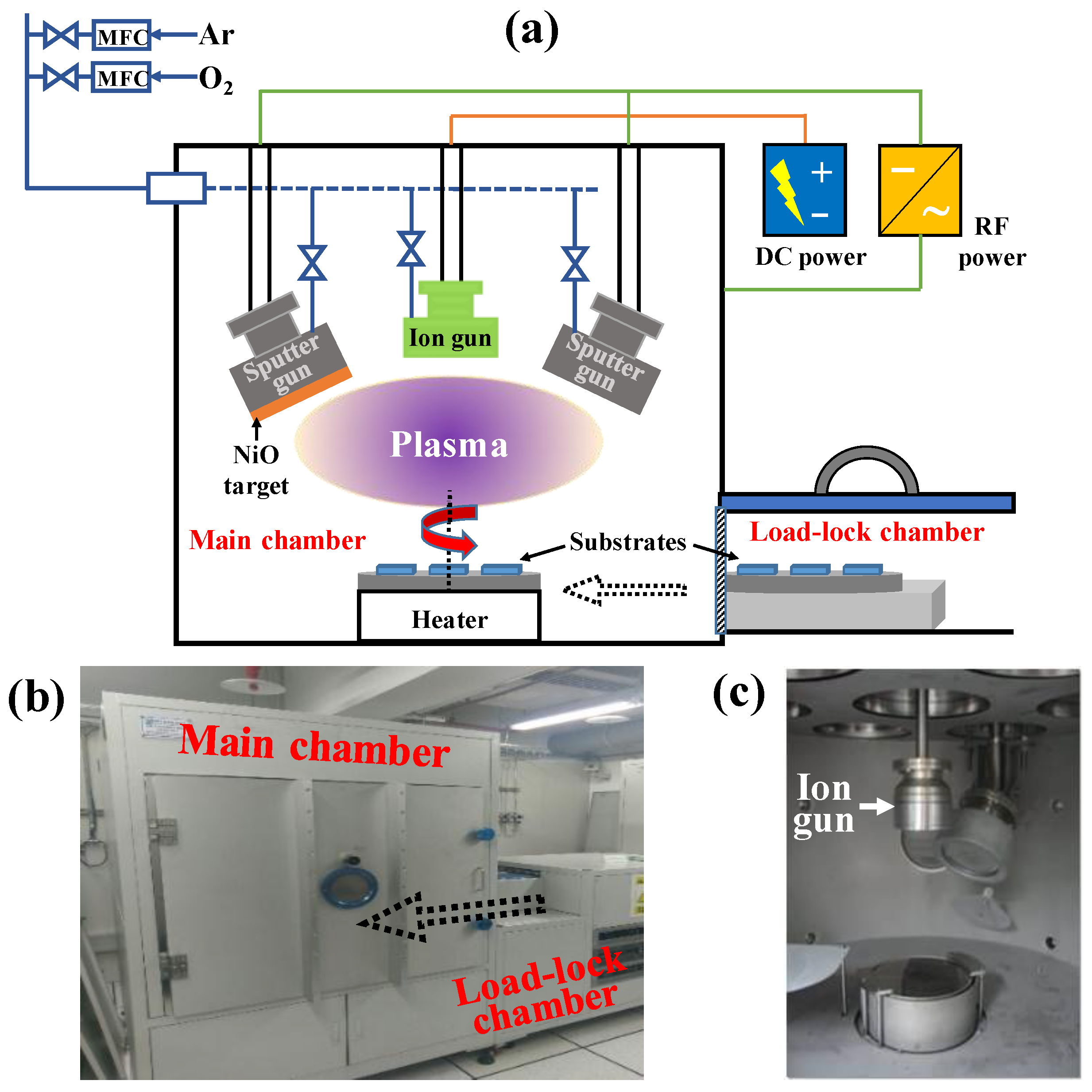
2. Materials and Methods

Ni1−xO thin films with a thickness of around 100 nm were deposited on rotating (10 rpm) Corning 1737F glasses at room temperature via in-line magnetron sputtering system (PSUVHL-200C, HOPE Vacuum Technology Co., Ltd., Taiwan). This system consists of a load-lock chamber and a main sputtering chamber, where the substrates loaded on the carrier can be moved horizontally from one chamber to another. The main advantage of this set-up is to enable the process of loading and unloading samples in the load-lock chamber while maintaining the vacuum in the main chamber. The illustration of the deposition system is shown in Figure 1. The ion gun is located perpendicular to the substrate holder, and the target is positioned next to the ion gun. The distance between the target and the substrate was kept at 20 cm. The sputtering chamber was pre-pumped until a base pressure higher than 6.7 × 10⁻⁵ Pa was achieved. Oxygen and argon were used as reactive gas mixtures. The working pressure was fixed at 0.67 Pa, while the oxygen flow ratios O2/(O2 + Ar) varied from 0% to 100%. A NiO target (purity 99.95%) with a diameter of 152.4 mm and a thickness of 3 mm was supplied by Ultimate Materials Technology Co., Ltd. (Taiwan) and powered by a radio frequency supply during the deposition process. The target power was set at 400 W. An assistance oxygen ion beam was powered using a DC supply (150 W) which bombarded the substrates during the deposition process. Other experimental parameters are summarized in Table 2.
The films’ thicknesses were examined using a surface profiler (Kosaka Surfcoder). The films’ compositions were measured using a JEOL JXA-8200 (JEOL, Tokyo, Japan) electron probe X-ray microanalyzer (EPMA). The films’ structural properties were detected with X-ray diffractometry (XRD, Philips PANalytical—X’Pert PRO MPD, Almelo, The Netherlands) in the 30°–70° angle range. The surface morphologies were observed via a JEOL JSM-6701F field emission scanning electron microscope (FE-SEM). The films’ carrier concentrations, carrier mobilities, and conductivities were analyzed using the Hall effect system (AHM-800B, Agilent Technologies, Santa Clare, CA, USA). Finally, the films’ optical properties were determined using an ultraviolet–visible-near infrared (UV–VIS-NIR) double beam spectrophotometer (JASCO-V670, JASCO, Tokyo, Japan) (λ = 200–900 nm).

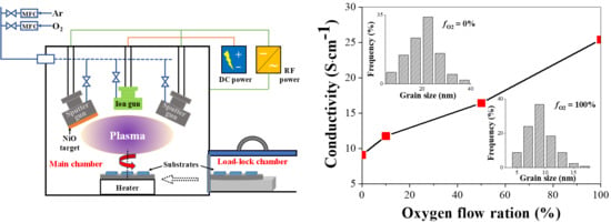
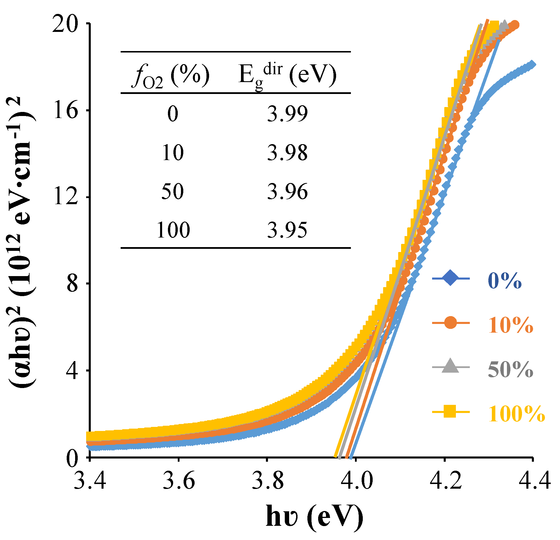
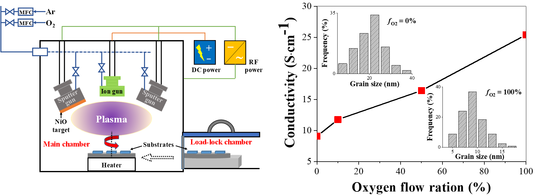
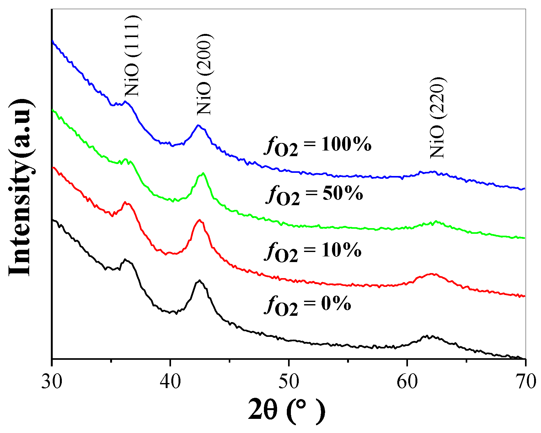
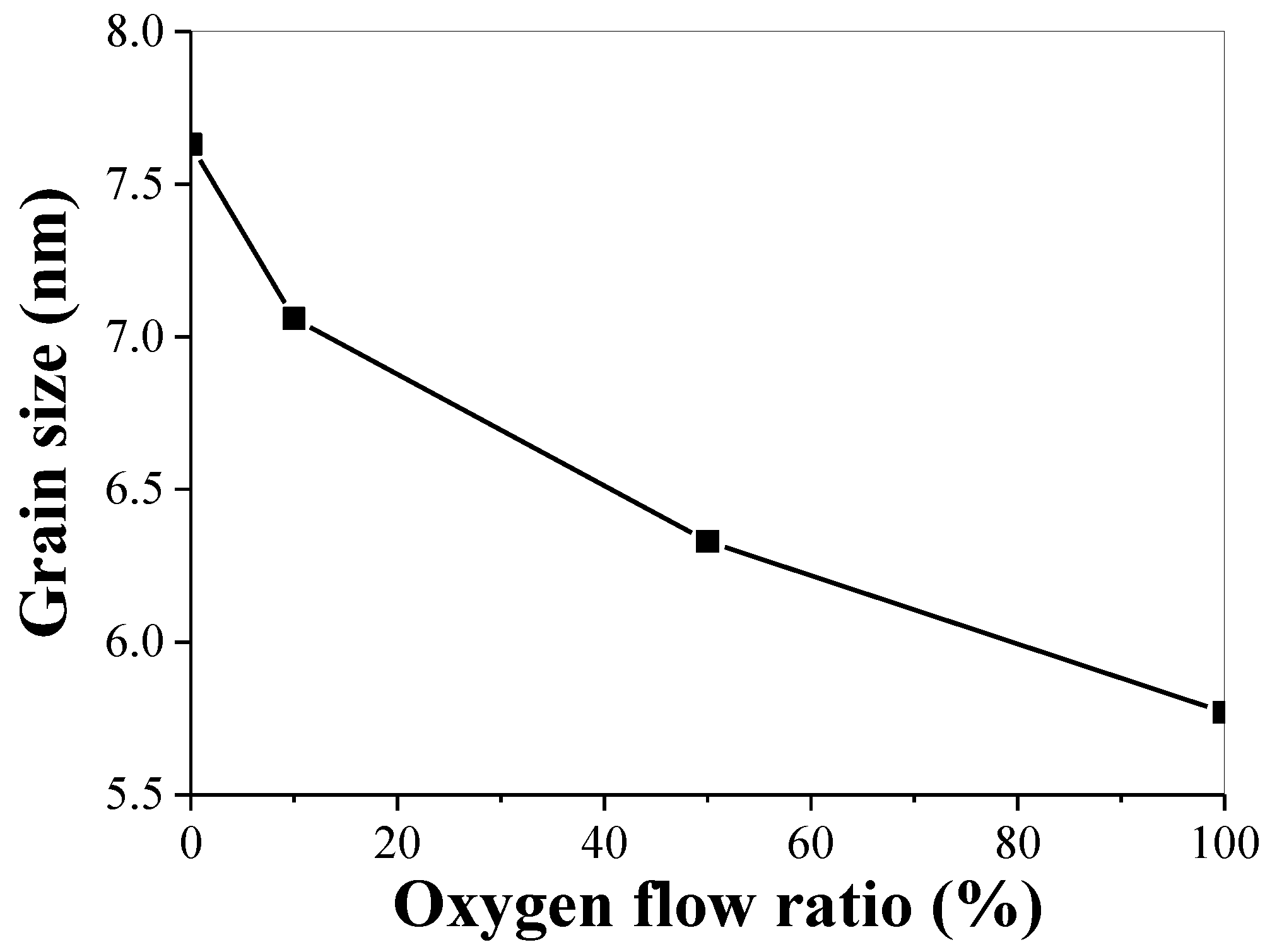
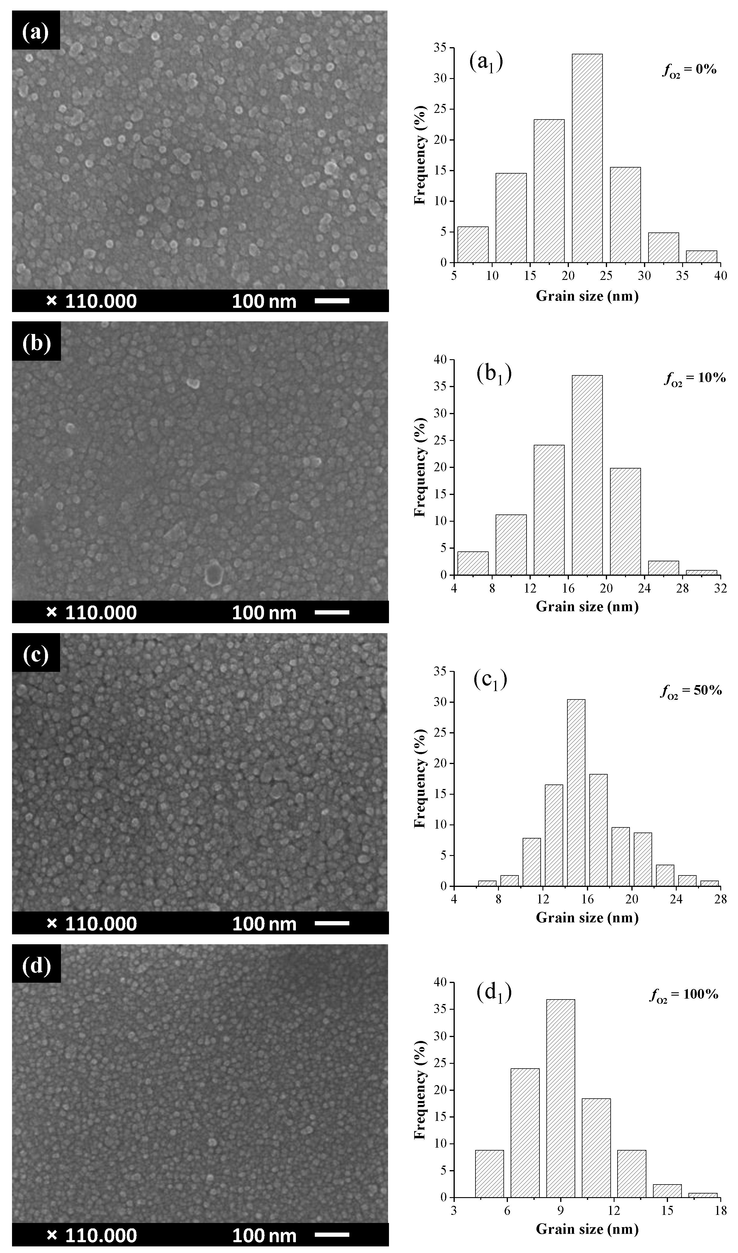
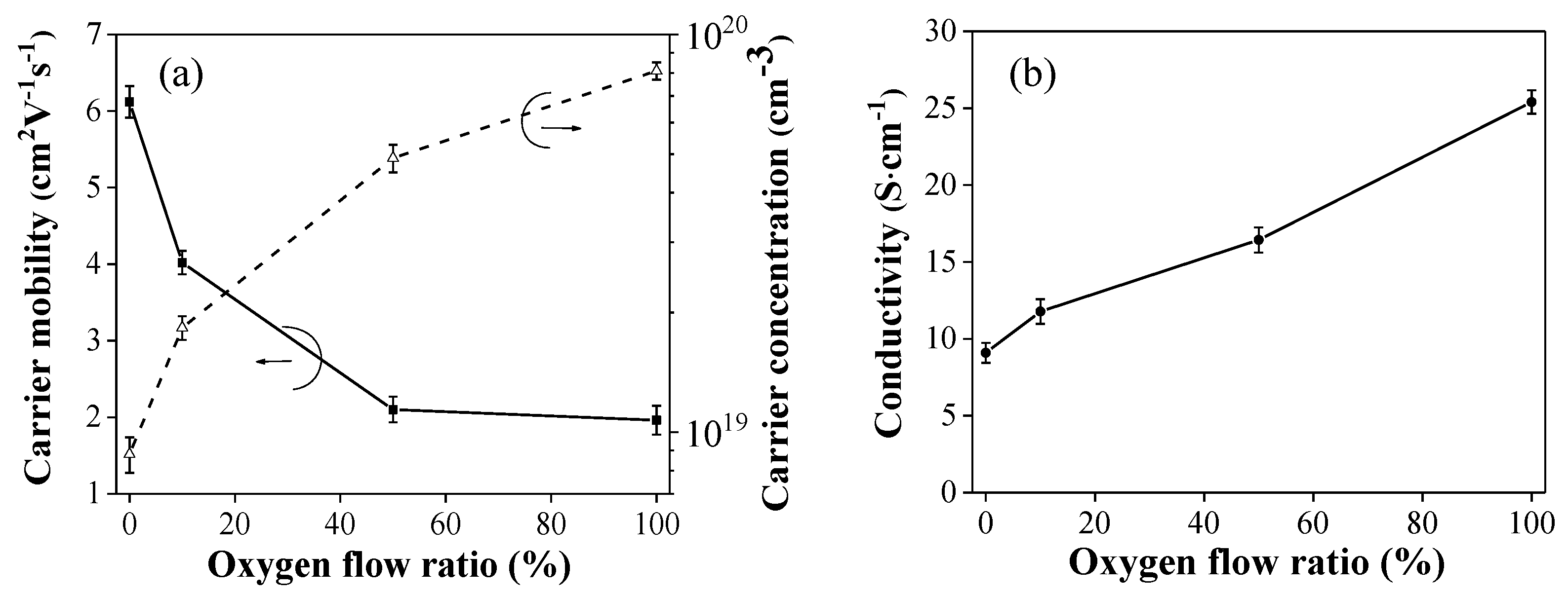
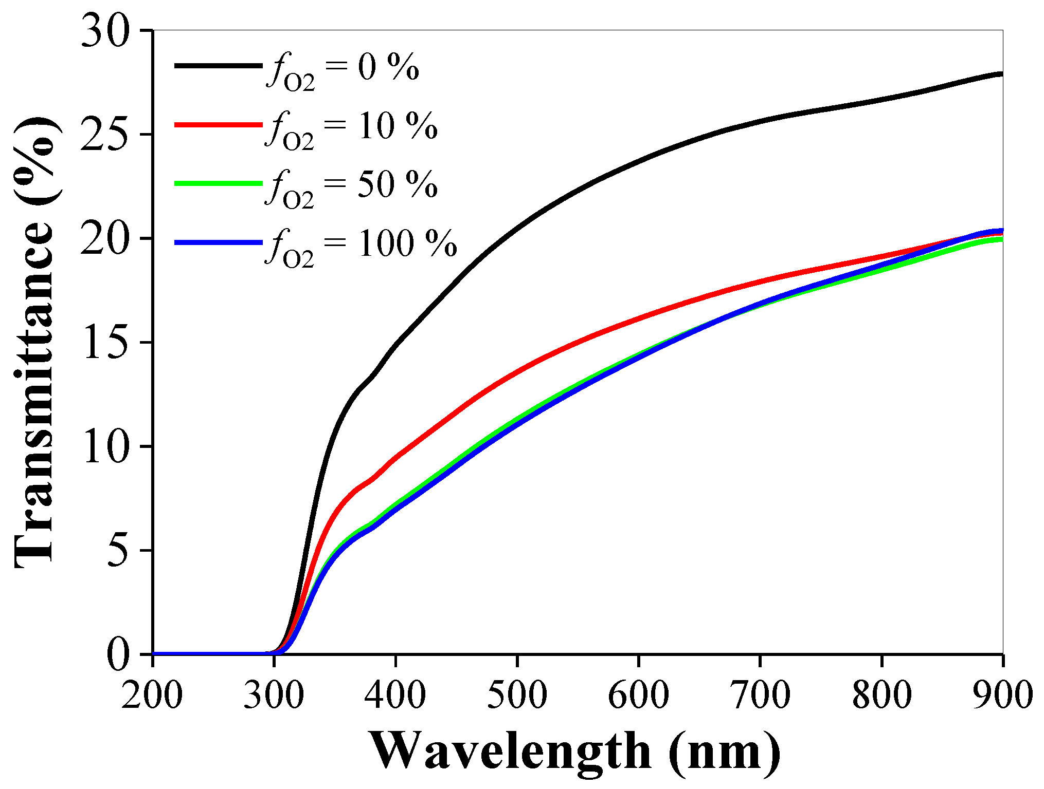
3. Results and Discussion

Figure 2 shows the variation of the oxygen content as a function of the oxygen flow ratio. With oxygen ion beam assistance, oxygen content is always higher than 50 at.%, indicating that all the films are non-stoichiometric. The oxygen-rich state contributes to the production of nickel vacancies, which has been confirmed to promote the films’ p-type conductivity [33,34]. With the oxygen flow ratio rising from 0% to 100%, the oxygen content gradually increases from 69.1 to 70.1 at.%. Compared with our previous work [32], where Ni1−xO thin films were deposited with oxygen ion beam assistance in pure Ar atmosphere, the effect of the oxygen flow ratio on the oxygen content is less important than that of ion source power. The variation of oxygen content in Ni1−xO films deposited at various ion source powers reported in our previous work is summarized in Table 3.
Figure 3 shows the X-ray diffraction patterns of Ni1−xO films deposited on glass substrates at various oxygen flow ratios. All the films are crystallized in cubic NiO phase. The diffraction peaks at around 37°, 43°, and 62° correspond well to the (111), (200), and (220) orientations of NiO. The relatively wide diffraction peaks imply that the films possess poor crystallization. In addition, the film’s crystallinity degrades with increasing oxygen flow ratio. This is attributed to more point defects such as nickel vacancies introduced into Ni1−xO films when they are deposited in higher fO2 conditions. A similar phenomenon is also reported by other groups, where Ni1−xO films were prepared by DC reactive magnetron sputtering and plasma-enhanced metalorganic chemical vapor deposition [35,36].
From XRD patterns, the crystallite size of Ni1−xO films can be calculated using Scherrer’s formula [37]
βhkl cosθhkl = Kλ/D
where βhkl is the full width at the half maximum (FWHM) of the diffraction peak, K is the shape factor, and D is the crystallite size corresponding to the reflective planes. The relationship between the grain size and the oxygen flow ratio is shown in Figure 4. The grain size of Ni1−xO films decreases from 7.63 to 5.77 nm with increasing oxygen flow ratios, implying that the excess oxygen can introduce some kinds of defects into NiO films, which affects the nucleation and growth of NiO grains. The decrement in the grain size reveals a degradation of the films’ crystallinity. It is identical with the broadening of NiO peaks shown in XRD analysis (Figure 3).
SEM observations of the top surfaces of Ni1−xO films are shown in Figure 5. The evolution of the films’ morphologies is evident. With the increment in oxygen flow ratios, the particle size gradually decreases. From the change in the size distribution versus the oxygen flow ratio (Figure 5a1–d1), the main diameter of the NiO particles for the films deposited without oxygen flow is about 22.5 nm. It then decreases from 18.0 to 15.0 nm and further decreases to 9.0 nm with fO2 increasing from 10% to 50% and then to 100%. With increasing oxygen flow ratios, the formation of VNi” defects contribute to the degradation of a film’s crystallinity, which further leads to the refinement of the NiO particles. This is consistent with the XRD results shown in Figure 3.
The relationship between the carrier concentration, Hall mobility, and electrical conductivity of Ni1−xO films and oxygen flow ratio is illustrated in Figure 6. Through Hall measurement, the p-type conductivity of Ni1−xO films is confirmed, regardless of the oxygen flow ratio. For the film deposited without oxygen, a relatively low carrier concentration of about 8.8 × 1018 cm−3 is obtained. This value monotonically increases to 8.1 × 1019 cm−3 when the oxygen flow ratio reaches 100%. The generation of the holes in O–rich Ni1−xO films is considered to originate from the following reaction:
1/2 O2 OO + VNi+ 2 NiNi
where VNi″ represents Ni2+ vacancies and NiNi denotes the formation of Ni3+ cations at Ni2+ sites. Nandy et al. [38] has reported that Ni2+ vacancies along with Ni3+ cations can be formed in non-stoichiometric Ni1−xO films deposited under O–rich conditions. Two holes associated with each cation vacancy can then be generated. In our case, with increasing oxygen flow ratios, more oxygen is introduced into the deposition system. Therefore, more Ni3+ cations and more positive carriers emerge. Thus, the carrier concentration increases. Meanwhile, the carrier mobility of Ni1−xO films decreases from 6.12 to 1.96 V·cm−1·s−1 with increasing oxygen flow ratios. This decrement is mainly caused by the degradation of the films’ crystallinity. The diminution in the grain size results in more grain boundaries in the films, which significantly obstruct the carrier movement and enhance the carrier scattering.
Regarding the films’ electrical conductivity (Figure 6b), the NiO film deposited without oxygen presents a conductivity of about 9.1 S·cm−1. As we have previously mentioned, all the films produced in the current work are oxygen enriched. The oxygen content in an Ni1−xO film can reach 69.12 at% even through there is no oxygen input. Hence, the holes originating in oxygen rich environments contribute to the films’ p-type conduction. With increasing oxygen flow ratios, a film’s conductivity is enhanced under the combined influence of carrier concentration and carrier mobility, indicating that the variation of carrier concentration plays a more important role in the films’ electrical properties. The film’s highest conductivity at around 25.4 S·cm−1 can be realized when fO2 reaches 100%.
The variation of films’ transmittance as a function of oxygen flow ratio is shown in Figure 7. As reported by Reddy [39] and Sun [21], the transmittance of off-stoichiometric NiO film is not ideal. All the films are pale brown or dark brown. With increasing oxygen flow ratios, more grain boundaries and point defects such as Ni2+ vacancies exist in the films. They can cause a large amount of visible light scattering, thereby reducing a film’s transmittance. Besides this, an absorption edge is observed at around 300 nm, originating from the charge transfer from the valence band to the conductive band. This absorption edge presents a red-shift to longer wavelengths with increasing oxygen flow ratio, implying a decrement in the films’ band gaps. A film’s optical band gap Eg can be calculated through the following equations [40,41]
α = (1/d) ln(1/T)
hʋ)1⁄n = A(hʋ − Eg)
where α is the absorption coefficient, d is the film thickness, T is the film’s transmittance, hʋ is the incident photon energy, and A is a constant. The exponent n depends on the type of transition. n = 1/2 and 2 for direct and indirect transition, respectively. The films’ direct band gaps versus oxygen flow ratio is depicted in Figure 8. A slight reduction in the films direct band gap from 3.99 to 3.95 eV is noted. This is consistent with the red-shift of the absorption edge shown in Figure 7. Generally, the fundamental band gap of NiO of about 3.9 eV is believed to correspond to the charge transition from valence band maximum to the unoccupied Ni 3d orbital [42,43,44,45]. This value is comparable to our results.
By comparing Figure 7 and Figure 8, it can be seen that a film’s transmittance obviously varies even though its band gap just present minor changes. We suspect that this behavior is mainly caused by the changes of the films’ crystallinity. As oxygen content increases in the film, the film’s crystallinity degrades (Figure 3), and the grain size evidently decreases (Figure 4 and Figure 5). Thus, more grain boundary scattering of the visible light occurs in the films deposited with a higher oxygen flow ratio. The films’ transmittances then deteriorate greatly.

4. Conclusions

Ni1−xO films have been prepared by oxygen ion beam assisted RF sputtering, and the influence of the oxygen flow ratio on the structural, morphological, and optoelectronic properties has been investigated. The XRD results indicate that all the films are crystallized in a cubic NiO structure. With an increase in the oxygen flow ratio, a degradation in films’ crystallization is detected. It is assumed to be caused by the introduction of point defects, such as nickel vacancies. Meanwhile, with increasing oxygen flow ratios, the carrier concentration is enhanced and the carrier mobility reduces. Films’ conductivity then improves. The holes originating from Ni2+ vacancies in O-rich conditions contribute to films’ p-type conductivity, whereas a film’s optical transmittance decreases when the oxygen flow ratio rises. This is attributed to more scattering of the visible light in the films with poor crystallinity deposited under higher fO2. When the oxygen flow ratio reaches 100%, the highest p-type conductivity of about 25 S·cm−1 is realized. In this condition, the films’ optical band gap is around 3.95 eV.

Author Contributions

Sheng-Chi Chen and Hui Sun conceived and designed the experiments; Wen-Chi Peng and Chao-Kuang Wen performed the experiments; Hui Sun and Xin Wang analyzed the data; Sheng-Chi Chen and Tung-Han Chuang contributed reagents, materials, and analysis tools; Hui Sun wrote the paper.

Acknowledgments

We gratefully acknowledge the Shandong Province Natural Science Foundation (ZR2018QEM002), the National Natural Science Foundation of China (No. 51172217), and the Ministry of Science and Technology of Taiwan (No. 105-2221-E-131-010) for their financial support. We also thank H.C.L. and C.Y.K. of the Instrumentation Center, National Taiwan University for their assistance with EPMA experiments.

Conflicts of Interest

The authors declare no conflict of interest.

References

  1. Frenzel, H.; Lajn, A.; Grundmann, M. One decade of fully transparent oxide thin-film transistors: Fabrication, performance and stability. Phys. Status Solidi R 2013, 7, 605–615. [Google Scholar] [CrossRef]
  2. Sun, H.; Liao, M.H.; Chen, S.C.; Li, Z.Y.; Lin, P.J.; Song, S.M. Synthesis and characterization of n-type NiO:Al thin films for fabrication of p-n NiO homojunctions. J. Phys. D 2018, 51, 105109. [Google Scholar] [CrossRef]
  3. Szyszka, B.; Dewald, W.; Gurram, S.K.; Pflug, A.; Schulz, C.; Siemers, M.; Sittinger, V.; Ulrich, S. Recent developments in the field of transparent conductive oxide films for spectral selective coatings, electronics and photovoltaics. Curr. Appl. Phys. 2012, 12, S2–S11. [Google Scholar] [CrossRef]
  4. Liu, Y.; Zhang, D. Synergetic effect in the multifunctional composite film of graphene-TiO2 with transparent conductive, photocatalytic and strain sensing properties. J. Alloys Compd. 2017, 698, 60–67. [Google Scholar] [CrossRef]
  5. He, L.X.; Tjong, S.C. Nanostructured transparent conductive films: Fabrication, characterization and applications. Mater. Sci. Eng. R 2016, 109, 1–101. [Google Scholar] [CrossRef]
  6. Wu, F.Y.; Tong, X.R.; Zhao, Z.; Gao, J.B.; Zhou, Y.W.; Kelly, P. Oxygen-controlled structures and properties of transparent conductive SnO2:F films. J. Alloys Compd. 2017, 695, 765–770. [Google Scholar] [CrossRef]
  7. Besleaga, C.; Stan, G.E.; Pintilie, I.; Barquinha, P.; Fortunato, E.; Martins, R. Transparent field-effect transistors based on AlN-gate dielectric and IGZO-channel semiconductor. Appl. Surf. Sci. 2016, 379, 270–276. [Google Scholar] [CrossRef]
  8. Mickan, M.; Helmersson, U.; Rinnert, H.; Ghanbaja, J.; Muller, D.; Horwat, D. Room temperature deposition of homogeneous, highly transparent and conductive Al-doped ZnO films by reactive high power impulse magnetron sputtering. Sol. Energy Mater. Sol. Cells 2016, 157, 742–749. [Google Scholar] [CrossRef]
  9. Wang, G.H.; Shi, C.Y.; Zhao, L.; Diao, H.W.; Wang, W.J. Transparent conductive Hf-doped In2O3 thin films by RF sputtering technique at low temperature annealing. Appl. Surf. Sci. 2017, 399, 716–720. [Google Scholar] [CrossRef]
  10. Al-Jawhari, H.A. A review of recent advances in transparent p-type Cu2O-based thin film transistors. Mater. Sci. Semicond. Process. 2015, 40, 241–252. [Google Scholar] [CrossRef]
  11. Sun, H.; Arab Pour Yazdi, M.; Chen, S.C.; Wen, C.K.; Sanchette, F.; Billard, A. Ag composition gradient CuCr0.93Mg0.07O2/Ag/CuCr0.93Mg0.07O2 coatings with improved p-type optoelectronic performances. J. Mater. Sci. 2017, 52, 11537–11546. [Google Scholar] [CrossRef]
  12. Cao, L.; Li, X.Y.; Wang, D.X.; Zhu, L.P. Li-doped NiMgO thin films as a promising p-type transparent conductive material with wide band-gap. Mater. Lett. 2013, 110, 73–75. [Google Scholar] [CrossRef]
  13. Sarmadian, N.; Saniz, R.; Partoens, B.; Lamoen, D. Easily doped p-type, low hole effective mass, transparent oxides. Sci. Rep. 2016, 6, 20446. [Google Scholar] [CrossRef] [PubMed]
  14. Li, M.H.; Yum, J.H.; Moon, S.J.; Chen, P. Inorganic p-type semiconductors: Their applications and progress in dye-sensitized solar cells and perovskite solar cells. Energies 2016, 9, 331. [Google Scholar] [CrossRef]
  15. Han, M.J.; Wang, J.; Deng, Q.L.; Wang, J.Y.; Li, W.W.; Zhang, P.; Li, C.Q.; Hu, Z.G. Effect of annealing temperature on structural optoelectronic properties and interband transitions of CuCrO2 nanocrystalline films prepared by the sol-gel method. J. Alloys Compd. 2015, 647, 1028–1034. [Google Scholar] [CrossRef]
  16. Tsay, C.Y.; Chen, C.L. Improved electrical properties of p-type CuGaO2 semiconductor thin films through Mg and Zn doping. Ceram. Int. 2017, 43, 2563–2567. [Google Scholar] [CrossRef]
  17. Zhang, Y.D. Thermal oxidation fabrication of NiO film for optoelectronic devices. Appl. Surf. Sci. 2015, 344, 33–37. [Google Scholar] [CrossRef]
  18. Wong, T.K.S.; Zhuk, S.; Masudy-Panah, S.; Dalapati, G.K. Current status and future prospects of copper oxide heterojunction solar cells. Materials 2016, 9, 271. [Google Scholar] [CrossRef] [PubMed]
  19. Loukil, A.; Boukhachem, A.; Ben Amor, M.; Ghamnia, M.; Raouadi, K. Effects of potassium incorporation on the structural, optical, vibrational and electrical properties of NiO sprayed thin films for p-type optical windows. Cream. Int. 2016, 42, 8274–8289. [Google Scholar] [CrossRef]
  20. Amiruddin, R.; Santhosh Kumar, M.C. Role of p-NiO electron blocking layers in fabrication of (P-N):ZnO/Al:ZnO UV photodiodes. Curr. Appl. Phys. 2016, 16, 1052–1061. [Google Scholar] [CrossRef]
  21. Sun, H.; Chen, S.C.; Chen, P.J.; Ou, S.L.; Liu, C.Y.; Xin, Y.Q. p-type conductive NiOx: Cu thin films with high carrier mobility deposited by ion beam assisted deposition. Cream. Int. 2018, 44, 3291–3296. [Google Scholar] [CrossRef]
  22. Iyengar, P.; Das, C.; Balasubramaniam, K.R. Photoelectrochemical performance of NiO-coated ZnO–CdS core-shell photoanode. J. Phys. D Appl. Phys. 2017, 50, 10LT01. [Google Scholar] [CrossRef]
  23. Dong, D.M.; Wang, W.W.; Dong, G.B.; Zhang, F.; He, Y.C.; Yu, H.; Liu, F.M.; Wang, M.; Diao, X.G. Electrochromic properties and performance of NiOx films and their corresponding all-thin-film flexible devices preparedby reactive DC magnetron sputtering. Appl. Surf. Sci. 2016, 383, 49–56. [Google Scholar] [CrossRef]
  24. Turgut, E.; Coban, O.; Saritas, S.; Tuzemen, S.; Yildirim, M.; Gur, E. Oxygen partial pressure effects on the RF sputtered p-type NiO hydrogen gas sensors. Appl. Surf. Sci. 2018, 435, 880–885. [Google Scholar] [CrossRef]
  25. Mei, B.; Permyakova, A.A.; Frydendal, R.; Bae, D.; Pedersen, T.; Malacrida, P.; Hansen, O.; Stephens, I.E.L.; Vesborg Peter, C.K.; Seger, B.; et al. Iron-treated NiO as a highly transparent p-type protection layer for efficient Si-based photoanodes. J. Phys. Chem. Lett. 2014, 5, 3456–3461. [Google Scholar] [CrossRef] [PubMed]
  26. Sun, K.; McDowell, M.T.; Nielander, A.C.; Hu, S.; Shaner, M.R.; Yang, F.; Brunschwig, B.S.; Lewis, N.S. Stable solar-driven water oxidation to O2(g) by Ni-oxide-coated silicon photoanodes. J. Phys. Chem. Lett. 2015, 6, 592–598. [Google Scholar] [CrossRef] [PubMed]
  27. Yu, J.G.; Rosso, K.M.; Bruemmer, S.M. Charge and ion transport in NiO and aspects of Ni oxidation from first principles. J. Phys. Chem. C 2012, 116, 1948–1954. [Google Scholar] [CrossRef]
  28. Dawson, J.A.; Guo, Y.; Robertson, J. Energetics of intrinsic defects in NiO and the consequences for its resistive random access memory performance. Appl. Phys. Lett. 2015, 107, 122110. [Google Scholar] [CrossRef]
  29. Grilli, M.L.; Menchini, F.; Dikonimos, T.; Nunziante, P.; Pilloni, L.; Yilmaz, M.; Piegari, A.; Mittiga, A. Effect of growth parameters on the properties of RF-sputtered highly conductive and transparent p-type NiOx films. Semicond. Sci. Technol. 2016, 31, 055016. [Google Scholar] [CrossRef]
  30. Predanocy, M.; Hotov, I.; Caplovicova, M. Structural, optical and electrical properties of sputtered NiO thin films for gas detection. Appl. Surf. Sci. 2017, 395, 208–213. [Google Scholar] [CrossRef]
  31. Li, L.; Wang, W.; He, L.; Zhang, J.; Wu, Z.; Zhang, B.; Liu, Y. Synthesis and characterization of p-type NiO films suitable for normally-off AlGaN/GaN HFETs application. Mater. Sci. Semicond. Process. 2017, 67, 141–146. [Google Scholar] [CrossRef]
  32. Chen, S.C.; Wen, C.K.; Kuo, T.Y.; Peng, W.C.; Lin, H.C. Characterization and properties of NiO films produced by rf magnetron sputtering with oxygen ion source assistance. Thin Solid Films 2014, 572, 51–55. [Google Scholar] [CrossRef]
  33. Ai, L.; Fang, G.J.; Yuan, L.Y.; Liu, N.S.; Wang, M.J.; Li, C.; Zhang, Q.L.; Li, J.; Zhao, X.Z. Influence of substrate temperature on electrical and optical properties of p-type semitransparent conductive nickel oxide thin films deposited by radio frequency sputtering. Appl. Surf. Sci. 2008, 254, 2401–2405. [Google Scholar] [CrossRef]
  34. Chen, S.C.; Kuo, T.Y.; Sun, T.H. Microstructures, electrical and optical properties of non-stoichiometric p-type nickel oxide films by radio frequency reactive sputtering. Surf. Coat. Technol. 2010, 205, S236–S240. [Google Scholar] [CrossRef]
  35. Reddy, A.M.; Reddy, A.S.; Lee, K.S.; Reddy, P.S. Effect of oxygen partial pressure on the structural, optical and electrical properties of sputtered NiO films. Ceram. Int. 2011, 37, 2837–2843. [Google Scholar] [CrossRef]
  36. Fujii, E.; Tomozawa, A.; Torii, H.; Talayama, R. Preferred orientations of NiO films prepared by plasma-enhanced metalorganic chemical vapor deposition. Jpn. J. Appl. Phys. 1996, 35, L328–L330. [Google Scholar] [CrossRef]
  37. Langford, J.I.; Wilson, A.J.C. Scherrer after sixty years: a survey and some new results in the determination of crystallite size. J. Appl. Crystallogr. 1987, 11, 102–113. [Google Scholar] [CrossRef]
  38. Nandy, S.; Saha, B.; Mitra, M.K.; Chattopadhyay, K.K. Effect of oxygen partial pressure on the electrical and optical properties of highly (200) oriented p-type Ni1−xO films by DC sputtering. J. Mater. Sci. 2007, 42, 5766–5772. [Google Scholar] [CrossRef]
  39. Reddy, Y.A.K.; Reddy, A.S.; Reddy, P.S. Influence of oxygen partial pressure on the structural, optical and electrical properties of Cu-doped NiO thin films. Phys. Scr. 2013, 87, 015801. [Google Scholar] [CrossRef]
  40. Demichelis, F.; Kaniadakis, G.; Tagliaferro, A.; Tresso, E. New approach to optical analysis of absorbing thin solid films. Appl. Opt. 1987, 26, 1737–1740. [Google Scholar] [CrossRef] [PubMed]
  41. Wang, K.L.; Xin, Y.Q.; Zhao, J.F.; Song, S.M.; Chen, S.C.; Lu, Y.B.; Sun, H. High transmittance in IR region of conductive ITO/AZO multilayers deposited by RF magnetron sputtering. Ceram. Int. 2018, 44, 6769–6774. [Google Scholar] [CrossRef]
  42. Ghosh, A.; Nelson, C.M.; Abdallah, L.S.; Zollner, S. Optical constants and band structure of trigonal NiO. J. Vac. Sci. Technol. A 2015, 33, 061203. [Google Scholar] [CrossRef]
  43. Gillen, R.; Robertson, J. Accurate screened exchange band structures for the transition metal monoxides MnO, FeO, CoO and NiO. J. Phys. Condens. Matter 2013, 25, 165502. [Google Scholar] [CrossRef] [PubMed]
  44. Sawatzky, G.A.; Allen, J.W. Magnitude and origin of the band gap of NiO. Phys. Rev. Lett. 1984, 53, 2339–2342. [Google Scholar] [CrossRef]
  45. Kurmaev, E.Z.; Wilks, R.G.; Moewes, A.; Finkelstein, L.D.; Shamin, S.N.; Kunes, J. Oxygen x-ray emission and absorption spectra as a probe of the electronic structure of strongly correlated oxides. Phys. Rev. B 2008, 77, 165127. [Google Scholar] [CrossRef]
Figure 1. (a) Schematic of an in-line magnetron sputtering system; (b) An external-view of an in-line magnetron sputtering system. The arrow shows the direction of the sample delivery from the load-lock chamber to the main chamber. (c) An internal-view of the main chamber. An ion gun is positioned perpendicularly to the substrate holder.
Coatings 08 00168 g001
Figure 2. Oxygen content in Ni1−xO films deposited with various oxygen flow ratios.
Coatings 08 00168 g002
Figure 3. Oxygen content in Ni1−xO films deposited with various oxygen flow ratios.
Coatings 08 00168 g003
Figure 4. The variation of the grain size of Ni1−xO films deposited with various oxygen flow ratios.
Coatings 08 00168 g004
Figure 5. Top surface SEM micrographs of Ni1−xO films deposited on glass substrates at various oxygen flow ratios and their corresponding size distribution of NiO particles: (a,a1) 0%, (b,b1) 10%, (c,c1) 50%, and (d,d1) 100%.
Coatings 08 00168 g005
Figure 6. (a) The carrier concentration, Hall mobility, and (b) electrical conductivity of Ni1−xO films versus oxygen flow ratio.
Coatings 08 00168 g006
Figure 7. The variation of the transmittance of Ni1−xO films as a function of oxygen flow ratio.
Coatings 08 00168 g007
Figure 8. The variation of the films’ direct band gaps as a function of the oxygen flow ratio.
Coatings 08 00168 g008
Table 1. The reported optoelectronic properties of NiO films.
FilmThickness (nm)Transmittance (%)Conductivity (S·cm−1)Carrier Concentration (cm−3)Carrier Mobility (V·cm−1·s−1)Ref.
NiO100~20–50 (visible region)0.57.26 × 101645.1[21]
NiO50~83–88 (visible region)~4.4 × 10¹⁹[25]
NiO3539 (at 550 nm)21.741.1 × 10210.1[29]
NiO10073.4 (at 550 nm)2.86 × 10−51.13 × 10136.41[30]
NiO~40–50 (visible region)3.8 × 10¹⁷[31]
Table 2. Sputtering parameters maintained during the deposition of Ni1−xO thin films.
ParametersValueParametersValue
Background pressure (Pa)<6.7 × 10⁻⁵SubstrateCorning 1737F glass
Working pressure (Pa)0.67Ion sourceO2
Working gasAr, O2Ion source power (W)150
TargetNiOTarget power (W)400
Hot substrateNoOxygen flow ratio
Films thickness (nm)100O2/(O2+Ar) (%)01050100
Table 3. The variation of oxygen content in Ni1−xO films deposited with various ion source powers [32].
Ion Source Power (W)Oxygen Content (at.%)
8059.5
10067.5
12068.6
15069.1

