The Gain of Low Thermal Expansivity via Phase Transition in Electroformed Invar


Department of Materials Science and Metallurgical Engineering, Sunchon National University, Suncheon 57922, Korea
*
Author to whom correspondence should be addressed.
Coatings 2018, 8(5), 169; https://doi.org/10.3390/coatings8050169
Submission received: 5 March 2018
/
Revised: 24 April 2018
/
Accepted: 1 May 2018
/
Published: 2 May 2018
(This article belongs to the Special Issue Thin Films and Patterned Structures by Electrochemical Methods)
Abstract
:In the organic light-emitting diode display industry, Invar exhibits anomalously low thermal expansivity and is, therefore, used as a material for fine metal masks, which are necessary components for the evaporation process of diode materials. We present an electroforming method for fabricating Fe-Ni alloys with a coefficient of thermal expansion lower than that of conventional Invar. The principle of controlling the thermal expansivity of electroformed Fe-Ni alloys is clarified in terms of the behavior of the phases constituting them. The cause of the Invar anomalies, which has not yet been fully elucidated, is explained by combining the Weiss model based on the electron configurations of Fe atoms and a model that we propose based on atom configurations.
1. Introduction
In the manufacturing processes of red-green-blue (RGB)-type organic light emitting diode (OLED) displays, Invar is used as a material for the fine metal mask (FMM), which guides the evaporated diode materials through its small holes onto the correct positions of the substrate glass. Because the hole size of the FMM should not change during the evaporation process, Invar, whose thermal expansivity approaches zero, must be used for the FMM material. The electroforming of Invar is an immediate hot issue in the RGB-type OLED display industries. To achieve high-quality color images in such displays, the FMM should be sufficiently thin that shadow zones due to the depth of the holes in the FMM do not hinder the evaporation of the diode materials.
Contrary to the conventional top-down method of producing Invar, a bottom-up approach of electroforming is a promising technology for producing very thin FMMs. Furthermore, producing an FMM via a single electroforming process using a patterned cathode is challenging. In the current work, Fe-Ni alloy foils were electroformed by employing a flat form of the cathode instead of the patterned cathode used for production of the FMM to definitely measure their coefficients of thermal expansion (CTEs) as a function of the alloy composition.
Whether electroformed Fe-Ni alloys can have a CTE in the order of approximately 1 μm/(m·K) at room temperature (as low as that of conventional Invar) when an Fe-36 wt %Ni alloy produced via the pyrometallurgical method [1] is used remains unclear. Addressing this issue involves elucidating the “Invar anomalies” that Guillaume discovered in 1897 [2] and will likely provide an innovative technology for industrial applications. Here, we present an electroforming method for fabricating Fe-Ni alloys with CTEs lower than that of conventional Invar and clarify the principle of controlling the thermal expansivity of the electroformed Fe-Ni alloys.
2. Materials and Methods
Under the bath conditions and process parameters given in Table 1, Fe-Ni alloys with different Ni contents ranging from 35 to 43 wt % were electrodeposited onto mirror-grade polished stainless steel substrates and then peeled from the substrates to fabricate free-standing sheets. Annealing was performed in an inert atmosphere of argon. The heating rate was 10 K/min, and isothermal annealing at the given temperatures was followed by water quenching.
The compositions of the electroformed alloy sheets were analyzed along the thickness direction in the cross-section of the samples using energy-dispersive X-ray spectroscopy (HIT S4300SE (II) 132-20, EDAX, Draper, UT, USA) with a field-emission scanning electron microscope (S-4300SE, HITACHI, Schaumburg, IL, USA). The CTEs of these electroformed sheets were measured in the temperature range from 298 to 333 K (25–60 °C) using a thermomechanical analyzer (TA Instruments Q400TMA, New Castle, DE, USA). The sheet dimensions were 16 mm × 5 mm, and the tests were performed using a 0.5 N load. These measurement conditions are used by almost all OLED FMM makers. The CTE measurements were performed on the samples with thicknesses of 7 µm and through-thickness compositional errors below 1.0 wt %.
The microstructures of the samples were observed using electron backscattering diffraction (EBSD). To achieve high-quality EBSD patterns in the field-emission scanning electron microscope, the samples were polished using a diamond paste of 1 μm and then using colloidal silica of 0.04 μm after conventional polishing procedures. The EBSD measurements were analyzed with the aid of the TSL software (Version 7.0), which sets up a tolerance angle of 15° and a confidence index (CI) value >0.1. X-ray diffraction using Cu-Kα was employed to determine the phases constituting the electroformed Fe-Ni alloys and to measure their lattice parameters. The X-ray tube voltage and current were 40 kV and 30 mA, respectively.
3. Results and Discussion
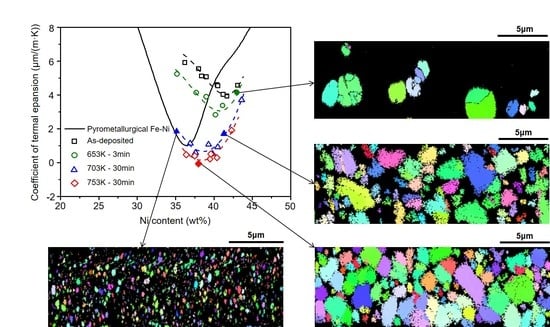
Fe-Ni alloys with different Ni contents ranging from 35 to 43 wt % were electroformed under the bath conditions and process parameters given in Table 1. Figure 1 shows the experimentally measured CTEs of the electroformed Fe-Ni alloys and the CTEs of Fe-Ni alloys found in the literature [1] for comparison. The CTEs as a function of the alloy composition of the electroformed Fe-Ni alloys differ substantially from the CTE curve of the Fe-Ni alloy produced using a pyrometallurgical method. The CTEs of the as-deposited Fe-Ni alloys are much higher than that of Invar, and the minimum CTE of approximately 4 μm/(m·K) occurs at a Ni composition of approximately 41 wt %. However, the CTEs of the electroformed Fe-Ni alloys were drastically reduced after heat treatment.
As presented in Figure 1, the electroformed Fe-Ni alloys with Ni contents ranging from 36 to 41 wt % after annealing above approximately 753 K (480 °C) for 30 min exhibited CTEs lower than that of conventional Invar [1] and similar to that of the commercial Invar applied currently for the OLED FMM. Therefore, Figure 1 raises several questions. First, why is the CTE in the as-deposited state of the electroformed Invar considerably higher than that of the pyrometallurgically produced Invar? Second, why do the CTEs of the electroformed Fe-Ni alloys decrease with heat treatment? Third, why does the composition of the alloy that exhibits the minimum CTE differ between the electroformed and pyrometallurgically produced Fe-Ni alloys? These phenomena are clarified based on the experimental results as follows.
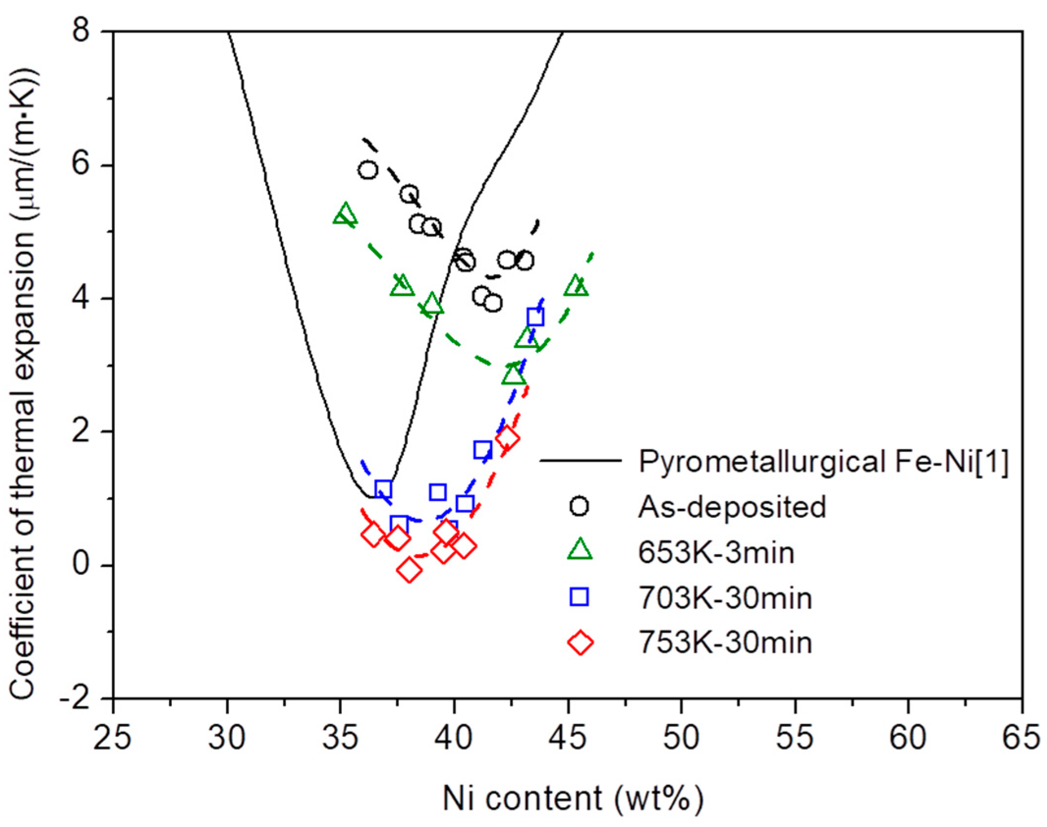
A sample of the Fe-Ni alloy sheet was intentionally fabricated to exhibit a compositional gradient along the thickness direction. To achieve this, the electroforming conditions were modified based on the conditions given in Table 1 as follows: 97 g/L of FeSO4·7H2O, 85 g/L of NiSO4·6H2O, pH = 2.5, current density rate of 0.2 mA/cm2∙min from 10 to 20 mA/cm2, and the other conditions were fixed. Figure 2a presents the compositional gradient from 40 wt % Ni at the surface (hereafter, the D-surface) that initially deposited onto the cathode to 31 wt % Ni at the other surface (hereafter, the F-surface) of a sample with a thickness of 10 µm. This compositional gradient was maintained within the measurement error after the samples were annealed at temperatures up to 753 K (480 °C). Figure 2b,c depict the X-ray diffraction (XRD) data collected for the D-surface and the F-surface, respectively. Because the thickness of the samples, 10 μm, could be penetrated by X-rays, the peaks in the XRD patterns of the D-surfaces reflect the structures of the sides of the F-surfaces and vice versa, although the XRD intensities decrease with increasing distance from the measurement position.
In the Fe-Ni alloy system, true thermodynamic equilibrium is never reached at temperatures below 653 K (380 °C) because of the slow inter-diffusion of Fe and Ni atoms. Consequently, the stable phases with body-centered cubic (BCC) structures contain as much as approximately 4 wt % Ni, and metastable BCC phases can contain up to approximately 25 wt % Ni [3]. However, in the as-deposited state of the electroformed Fe-Ni alloys fabricated in the current work, the BCC phase, hereafter denoted by α, and the face-centered cubic (FCC) phase, hereafter denoted by γ′, coexist in the composition range between 36 and 41 wt % Ni. The single α phase exists in the compositions with less than 36 wt % Ni, and the single γ′ phase exists in the compositions of more than 41 wt % Ni. The authors of a previous study [4] reported similar results concerning the relation between the phases and the alloy compositions in electrodeposits fabricated using bath conditions and process parameters that differ from those used in the present work. The broadening of the peaks observed in the XRD patterns of the as-deposited state are attributed to the electroformed Fe-Ni alloy that consists of nanometer-sized crystallites. The mean grain size calculated using Scherrer’s formula [5], i.e., t = 0.9λ/BcosθB, is approximately 7 nm. A previous study [6] reported that the morphology of nanometer-sized grains observed using a transmission electron microscope is equiaxed.
The EBSD orientation maps observed in the cross-sections of the annealed samples are given in Figure 2d–f. When the electroformed Fe-Ni alloy with the compositional gradient shown in Figure 2a was annealed at 653 K (380 °C) for 3 min, abnormal grain growth (AGG) of the nanometer-sized crystallites occurred only in the section of the sample with a Ni content > 36 wt %, i.e., to a distance approximately 4 μm from the D-surface, see Figure 2d. Because the resolution limit of the EBSD measurements is 20 nm, the nanocrystalline section of the sample appears dark in the EBSD map. As presented in Figure A1, AGG occurs during annealing above 623 K (350 °C) in the electroformed nanocrystalline Fe-Ni alloys with the FCC structure [7]. Therefore, as evident in Figure 2d, AGG occurred only in the γ′ phase; the α phase maintained the nanocrystalline state. Hereafter, the FCC phase formed by AGG during annealing is denoted by γ″ to distinguish it from γ′, which is the as-deposited FCC phase.
In Figure 2e, which shows the EBSD map for the cross-section of the sample annealed at 703 K (430 °C) for 30 min, grain growth is also observed in a part of the nanocrystalline α phase, but far from AGG in terms of the scale change in grain size. Importantly, it was analyzed using EBSD that the grown grains were transformed into the FCC structure, i.e., the α → γ″ phase transition occurred. Notably, grain growth of the α phase was not observed. The dark area in the EBSD map represents the α phase that has maintained its nanocrystalline state, which is confirmed by broadening of the α{110}-peak in the XRD pattern of the F-surface of the sample as depicted in Figure 2c. When the sample was annealed at 753 K (480 °C) for 30 min, as observed in Figure 2f, a small portion of the α phase still maintained the nanocrystalline state among far more developed grains. Despite the microstructure changes, such as the α → γ″ phase transition and grain growth of the transformed γ″ phase, the through-thickness compositional gradient is maintained within the measurement error, as shown in Figure 2a. This result indicates that the microstructure changes occurred without a compositional change.
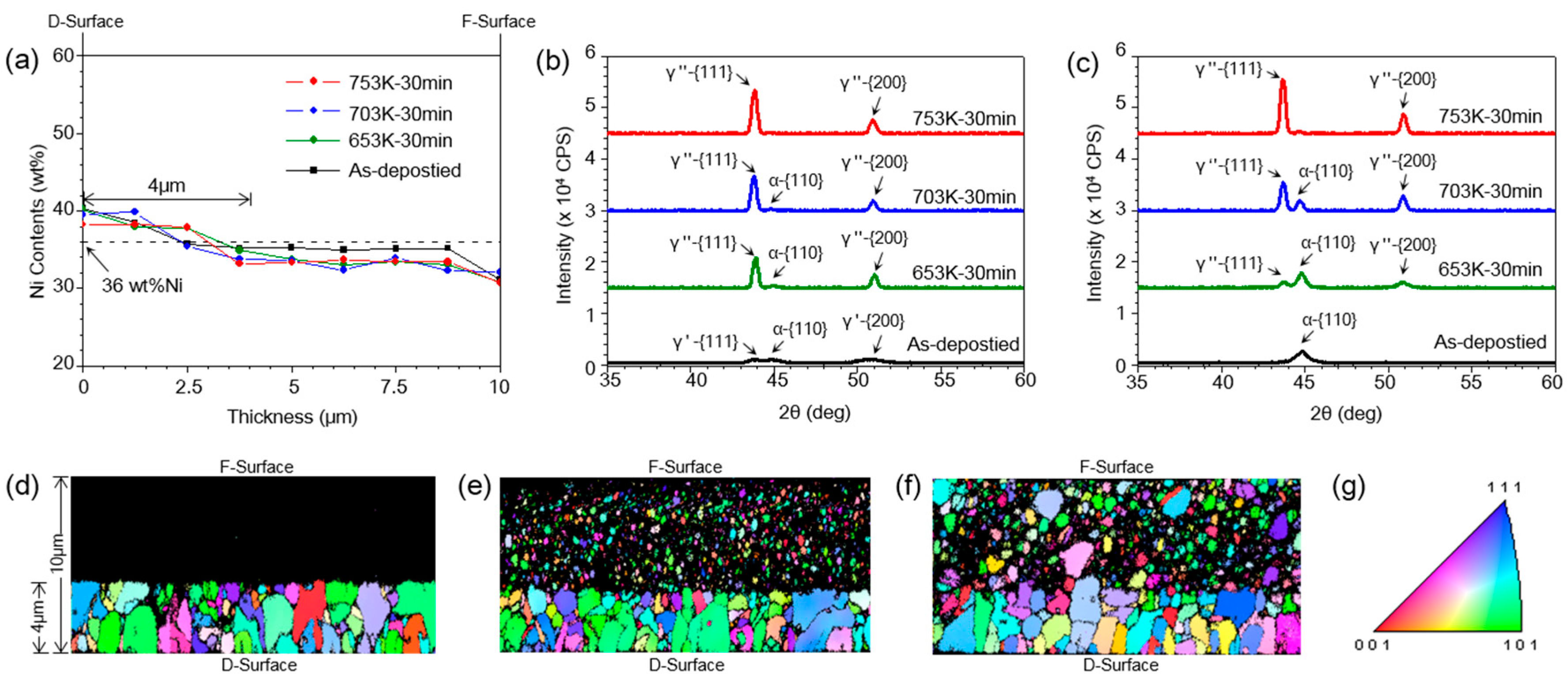
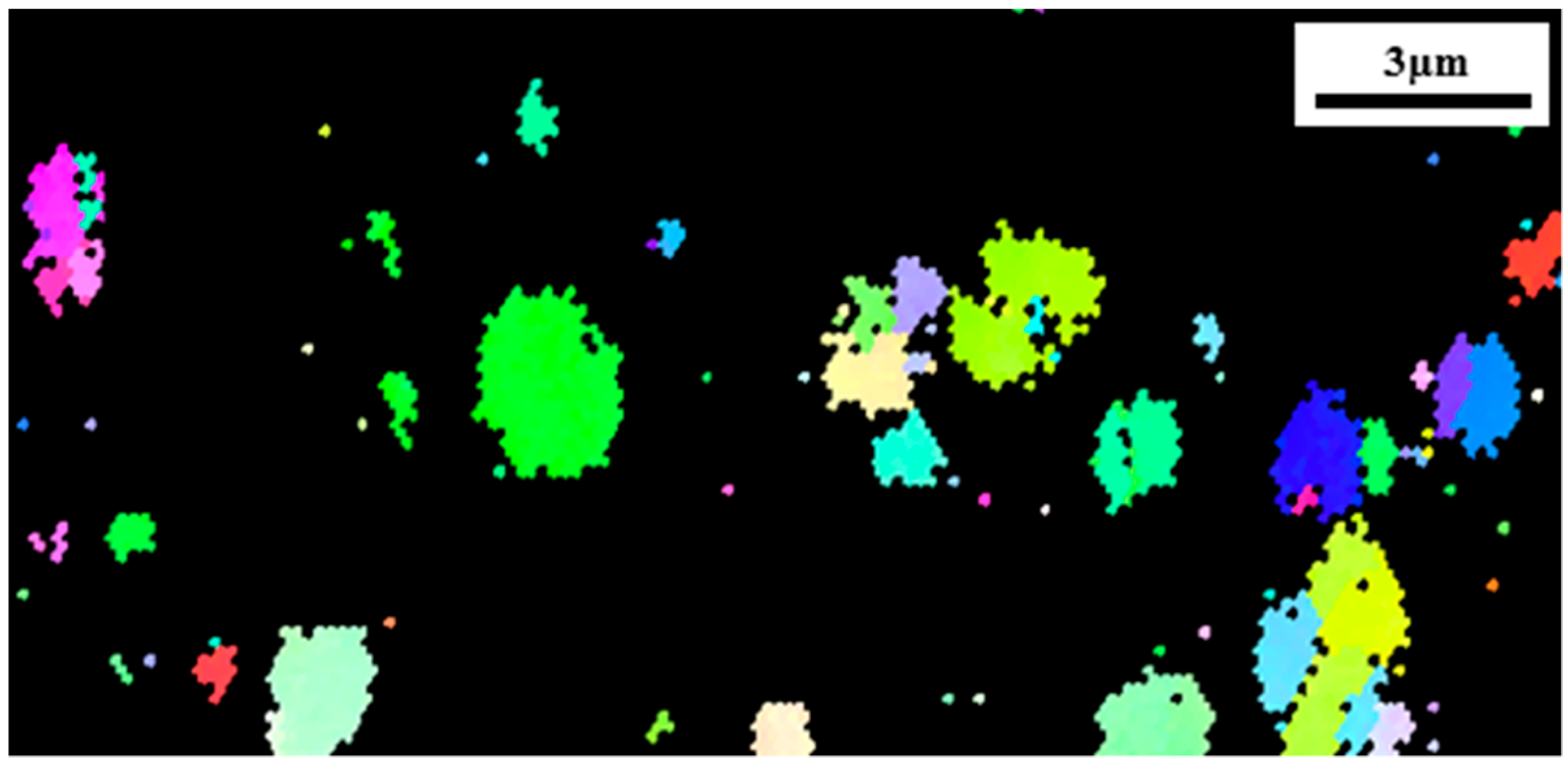
To examine the stability of the α phase in the as-deposited state and the phase transition that occurs during annealing, the Fe-35 wt % Ni alloy sheet consisting of the single α phase was electroformed. The process conditions given in Table 1 were controlled to make the α phase possess two different morphologies of grains, i.e., one is nanocrystalline and the other is columnar. Figure 3a shows the EBSD map of the cross-section of the sample and the XRD data corresponding to the D-surface. In the entire sample thickness of approximately 30 μm, the initially deposited section of the sample up to approximately 5 μm from the D-surface consisted of the nanocrystalline α phase (dark area in the EBSD map) and a columnar type of large-sized grains, represented by red color, developed in the other section.
When this sample was annealed at 703 K (430 °C) for 30 min and then subsequently water-quenched, as shown in Figure 3b, the spherical γ″ grains were grown. These γ″ grains were formed by the transformation of the nanocrystalline α phase; additionally, the columnar grains of the α phase transformed into the γ″ phase without a morphological change (the γ″ phase is represented by the green color in Figure 3b). The α → γ″ phase transition occurring in the nanocrystalline region is more homogeneous than that of the columnar grains. This effect will be discussed later. The amount of the remaining α phase that did not transform into the γ″ phase can be predicted in the Fe-Ni equilibrium phase diagram [8].
Notably, in Figure 3, the α → γ″ phase transition can neither occur through atomic diffusion [9] nor a massive transformation [10] reported in the Fe-Ni alloy system. The annealing temperature of 703 K (430 °C) is too low for Fe and Ni atoms to move extensively. Another important point concerning Figure 3 is that the α phase is metastable with respect to maintaining the nanostructure in the as-deposited state but is too unstable for grain growth to occur during annealing. When the grains of the α phase are thermally activated, the transformation of the α phase into the stable γ″ phase may occur faster prior to the occurrence of grain growth in the α phase.
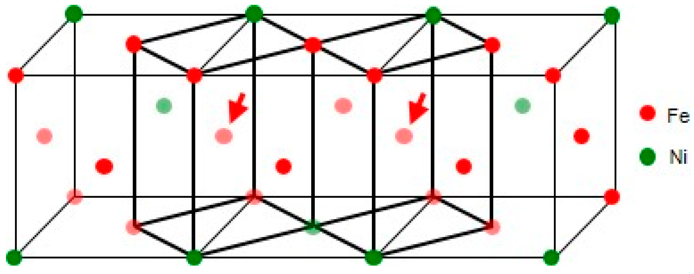
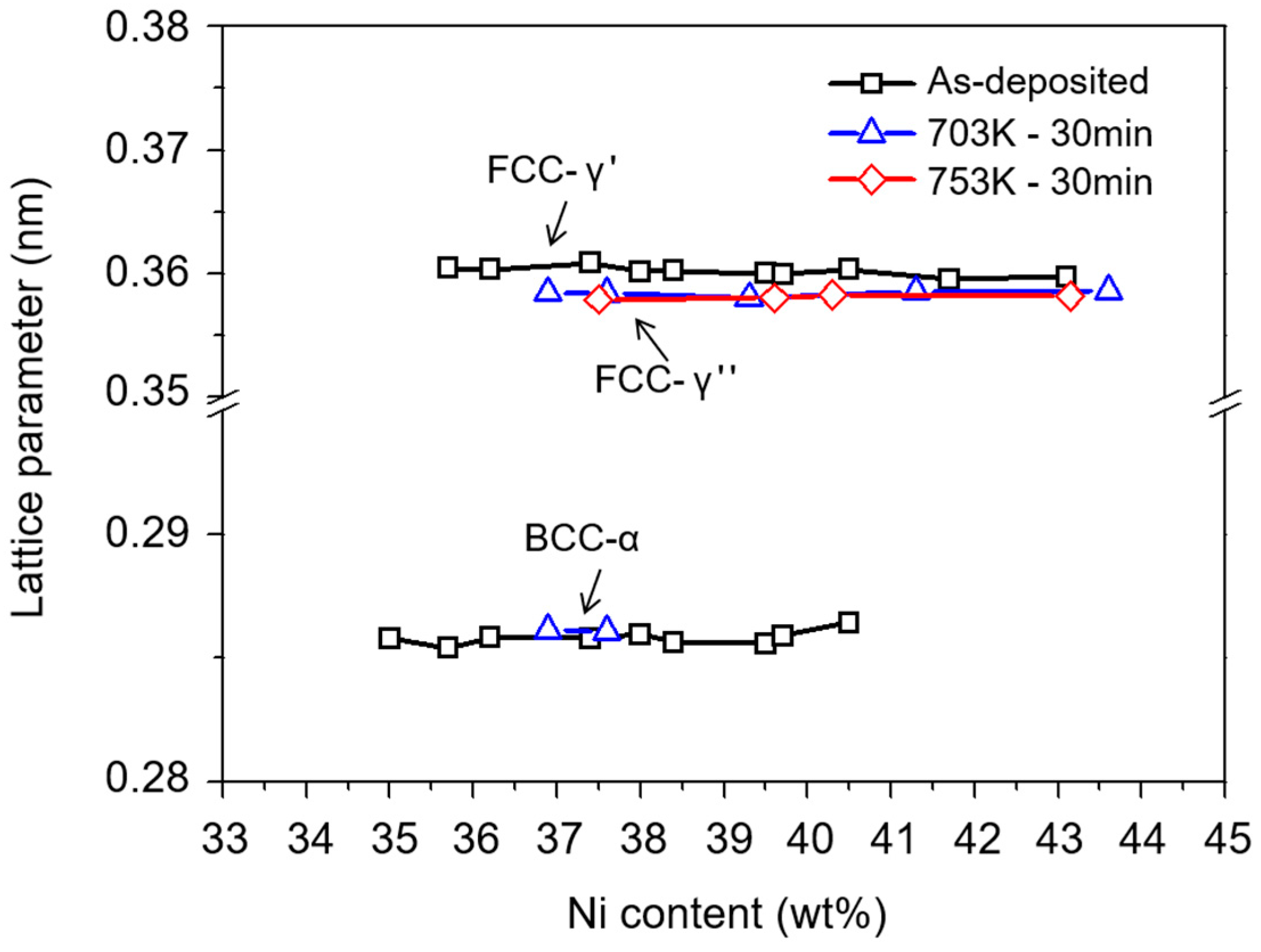
The electroformed Fe-36 wt % Ni alloy consists of a mixture of the α and γ′ phases in the as-deposited state and of the single γ″ phase when fully annealed. Figure 4 gives an example of the atom configurations for the Fe-36 wt % Ni (Fe-35 at.% Ni) composition, where Fe and Ni atoms are represented by red and green colors, respectively. The FCC structure, as drawn by thin lines, is equivalent to the body-centered tetragonal (BCT) structure. The BCT structure may transform into the BCC structure by altering the interatomic distances without extensive atomic movement [11]. The lattice parameters of the α and γ′ phases measured using XRD were 0.286 nm (2.86 Å) and 0.360 nm (3.60 Å), respectively (see Figure A2). Thus, the spatial volumes occupied by the same numbers of atoms in occupy each phase are almost equal, i.e., 2 × 2.863/3.603 ≒ 1. This structural accommodation enables the unstable α phase to co-deposit with the relatively stable γ′ phase during electroforming for Ni-rich compositions ranging from 36 to 41 wt %.
The difference of which phase, α or γ′, is electrodeposited for the Fe-36 wt % Ni composition modifies not only the interatomic distances to fit the corresponding phase but also neighboring circumstances of the Fe atoms. Consider the Fe atoms indicated by the arrows seen in Figure 4. The number of the nearest-neighbor Fe atoms with respect to each Fe atom is either 5 for the BCC structure or 8 for the FCC structure. Therefore, the α → γ″ phase transition, as shown in Figure 3, corresponds to the change from 5 to 8 in the number of the nearest-neighbor Fe atoms. When the Fe-Ni alloy assumes the FCC structure, the maximum number of the nearest-neighbor Fe atoms is 8 at compositions near 36 wt % Ni and decreases with increasing Ni content. In the case in which the number of nearest-neighbor Fe atoms for the BCC structure is 8 at maximum, it is pure Fe. Chikazumi [12] demonstrated that the Invar anomalies are associated with the energy state of each Fe atom, which strongly depends on the number of nearest-neighbor Fe atoms.
As shown in Figure 1, for the Fe-36 wt % Ni composition, the CTE of the as-deposited state of the electroformed Invar, which is overwhelmingly dominated by the α phase, is approximately 6 μm/(m·K), whereas it approaches zero in the sample consisting of the single γ″ phase after annealing at 753 K (480 °C) for 30 min. This phenomenon where the CTE decreases because of the α → γ″ phase transition is readily explained by the increase in the number of the nearest-neighbor Fe atoms from 5 to 8. CTEs lower than that of conventional Invar are observed for the samples consisting of the single γ″ phase with Ni contents ranging from 36 to 41 wt %, thus exhibiting a decrease in the number of the nearest-neighbor Fe atoms from 8 to 7 after annealing at 753 K (480 °C) for 30 min. However, even in the samples consisting of the single γ″ phase, when the Ni content is increased to more than 41 wt %, the CTE drastically increases because of the decrease in the number of the nearest-neighbor Fe atoms.
The fact that the Fe-36–41 wt % Ni alloys annealed at 703 K (430 °C) for 30 min exhibit CTEs greater than those of the alloys of the single γ″ phase is attributable to the co-existence of the α phase with the reduced number of nearest-neighbor Fe atoms. Thus, the presence of a small amount of the γ″ phase is responsible for the CTEs of the samples annealed at 653 K (380 °C) for 3 min decreasing only slightly compared with the CTE of the as-deposited material. Nagayama et al. [13] also reported a substantial decrease of the CTEs due to the BCC → FCC phase transition in electroformed Fe-Ni alloys that exhibited CTEs greater than that of conventional Invar. It is noted that the anomalous co-deposition behavior of Fe and Ni ions during the electrodeposition of Fe-Ni alloys appears significant with increasing Fe contents. As a result, the α phase would grow into a columnar type of large-sized grains rather than nanocrystals as observed in the materials of Nagayama et al. [13], see also Figure 3. The development of the columnar structure in the electroformed Fe-Ni alloys results in through-thickness inhomogeneity of the alloy composition. In this case, the gain of low thermal expansivity is difficult in the final products even after sophisticated heat treatment. The homogeneous α → γ″ phase transition that takes place in nanostructured Fe-Ni alloys might lead to their low thermal expansivity. For this, the process conditions given in Table 1 should be accurately applied for electroforming alloys with Fe-rich compositions.
The previous discussion clarifies the first issue of why the CTE in the as-deposited state of the electroformed Invar is considerably higher than that of pyrometallurgicallay produced Invar and the second issue of why the CTEs of the electroformed Fe-Ni alloys decrease via heat treatment that were brought up by Figure 1. The third issue of why the alloy composition for the minimum CTE differs for the electroformed and pyrometallurgically produced Fe-Ni alloys can also be clarified based on the number of nearest-neighbor Fe atoms. The minimum Ni content at which the single γ′ phase can exist in the as-deposited state is approximately 41 wt %; thus, the maximum number of nearest-neighbor Fe atoms is 7. It follows that the minimum CTE in the as-deposited state of the electroformed Invar is observed for the Fe-41 wt % Ni composition.
However, to explain significant difference of the CTE vs. composition curve between the electroformed Invar and the conventional Invar, other factors such as grain boundary phenomena and alloying elements should be considered together with the effect of the phase structure as mentioned above. The as-deposited Invar consisting of nanometer-sized crystallites possesses much larger amount of grain boundaries than the coarse-grained conventional Invar. It has recently been reported that the grain boundary segregation and films of grain boundary phases can allow to “hide” a lot of atoms in grain boundaries [14] and thus change the concentration in the matrix [15]. These grain boundary phenomena can make the CTE curve shift towards the Ni richer composition as well as the higher CTE value in the as-deposited Invar in comparison to the conventional Invar as observed in Figure 1. On the other hand, there is a fundamental difference between the electroformed and pyrometallurgically produced Fe-Ni alloys in terms of alloying elements. The Fe-Ni alloys fabricated in the current work are a nearly perfect binary Fe-Ni alloy system while most of pyrometallurgically produced Invar alloys contain various kinds of alloying elements [16]. It is well known that different commercial Invar alloys reveal different relationships of CTE vs. composition [1]. Effects of alloying elements might be related to the phenomenon that the Invar effect drastically disappears except for around 36 wt % Ni composition in the pyrometallurgically produced Invar while the electroformed Fe-Ni binary alloys after annealing perform low thermal expansivity persistently from 36 up to 41 wt % Ni contents. This is a striking result for practical applications because the anomalous co-deposition behavior occurring during the deposition process is relatively moderated with increasing Ni content.
Finally, the decrease of the CTEs due to the γ′ → γ″ state transition in the alloys consisting of a single FCC phase, i.e., those with Ni contents greater than 41 wt %, should be clarified. In fact, the α → γ″ phase transition that occurs during the annealing of the electroformed Fe-Ni alloys may result from the α → γ′ phase transition followed by the γ′ → γ″ state transition. Figure A2 reveals that the lattice parameter of the FCC phase decreases from 0.360 to 0.358 nm (3.60–3.58 Å) because of the γ′ → γ″ state transition. The anomalously low thermal expansivity of Invar originates from instability of ferromagnetism around the Invar compositions [12]. This is strongly related to the electron spin state of Fe atoms. The Weiss model [17], which serves as the basis of the prevailing models of the Invar anomalies, explains that Fe atoms of the FCC structure of an Fe-Ni alloy can assume two different electron configurations, i.e., the low-spin state and the high-spin state, and that the “Invar effect” occurs because of the thermal activation of the low-spin state, which possesses a smaller atomic volume. In terms of the lattice parameter, the γ′ and γ″ phases observed in the electroformed Fe-Ni alloys may correspond to the high-spin state and the low-spin state, respectively, in the electron configurations [18]. The lattice parameter of the commercial Invar applied currently for the OLED FMM is approximately 0.358 nm (3.58 Å) at room temperature as measured using XRD under the same conditions used in the present study.
4. Conclusions
Electroformed Fe-Ni alloys with nanometer-sized grains in the as-deposited state can exhibit low thermal expansivity via heat treatment, which makes these alloys consist of a single γ″ phase with an atomic configuration that maximizes the number of nearest-neighbor Fe atoms. Significant difference of the CTE vs. composition curve between the electroformed Invar and the conventional Invar could be explained in terms of the effect of the phase structure with considering together grain boundary phenomena and alloying elements.
Author Contributions
Y.B.P. designed the research. I.G.K. performed the experiments and measurements. Y.B.P. analyzed the data and wrote the manuscript.
Funding
This study was supported by Basic Science research Program through the National Research Foundation of Korea (NRF) funded by the Ministry of Science, ICT & Future Planning (No. 2013R1A1A2013772).
Conflicts of Interest
The authors declare no conflict of interest.
Appendix A
Figure A1.
Abnormal grain growth occurring in the FCC phase. The EBSD map shows abnormal grain growth occurring during annealing at 673 K (400 °C) for 1 min in the electroformed Fe-43 wt % Ni alloy consisting of the single γ′ phase. The dark area indicates the nanometer-sized crystallites smaller than the step size of the EBSD scanning.

Figure A2.
Lattice parameters of the α, γ′ and γ″ phases. The XRD data were collected for the same samples used for Figure 1.
Figure A2.
Lattice parameters of the α, γ′ and γ″ phases. The XRD data were collected for the same samples used for Figure 1.

References
- Baker, H. Metal Handbook, 9th ed.; ASM: Washington, DC, USA, 1979. [Google Scholar]
- Guillaume, C.É. Recherches sur les aciers au nickel. Dilatations aux températures élevées; résistance électrique. C. R. Acard. Sci. 1897, 125, 235–238. [Google Scholar]
- Reuter, K.B.; Williams, D.B.; Goldstein, J.J. Determination of the Fe-Ni Phase Diagram below 400 °C. Metall. Trans. A 1989, 20, 719–725. [Google Scholar] [CrossRef]
- Tabakovic, I.; Inturi, V.; Thurn, J.; Kief, M. Properties of Ni1−xFex (0.1 <x <9) and Invar (x = 0.64) alloys obtained by electrodeposition. Electrochim. Acta 2010, 55, 6749–6754. [Google Scholar]
- Cullity, B.D. Elements of X-ray Diffraction, 2nd ed.; Addison-Welsey: Boston, MA, USA, 1978. [Google Scholar]
- Seo, J.H.; Kim, J.K.; Yim, T.H.; Park, Y.B. Texture and grain growth in nanocrystalline Fe-Ni alloys. Mater. Sci. Forum 2005, 475–479, 3483–3488. [Google Scholar] [CrossRef]
- Kim, J.K.; Seo, J.H.; Park, Y.B. Grain growth and texture development in nanostructured invar alloy. Mater. Sci. Forum 2004, 467–470, 1313–1318. [Google Scholar] [CrossRef]
- Kubaschewski, O. Iron-Binary Phase Diagrams; Springer: New York, NY, USA, 1982. [Google Scholar]
- Larsson, H.; Borgenstam, A. Trans-interface diffusivity in the Fe-Ni system. Scr. Mater. 2007, 56, 61–64. [Google Scholar] [CrossRef]
- Borgenstam, A.; Hillert, M. Massive transformation in the Fe-Ni system. Acta Mater. 2000, 48, 2765–2775. [Google Scholar] [CrossRef]
- Wechsler, M.S.; Lieberman, D.S.; Read, T.A. On the theory of the formation of martensite. Trans. AIME 1953, 197, 1503–1515. [Google Scholar]
- Chikazumi, S. Invar anomalies. J. Magn. Magn. Mater. 1979, 10, 113–119. [Google Scholar] [CrossRef]
- Nagayama, T.; Yamamoto, T.; Nakamura, T. Thermal expansions and mechanical properties of electrodeposited Fe-Ni alloys in the Invar composition range. Electrochim. Acta 2016, 205, 178–187. [Google Scholar] [CrossRef]
- Straumal, B.B.; Sauvage, X.; Baretzky, B.; Mazilkin, A.A.; Valiev, R.Z. Grain boundary films in Al-Zn alloys after high pressure torsion. Scr. Mater. 2014, 70, 59–62. [Google Scholar] [CrossRef]
- Straumal, B.B.; Protasova, S.G.; Mazilkin, A.A.; Goering, E.; Schütz, G.; Straumal, P.B.; Baretzky, B. Ferromagnetic behavior of ZnO: The role of grain boundaries. Beilstein J. Nanotechnol. 2016, 7, 1936–1947. [Google Scholar] [CrossRef] [PubMed]
- Pearson, W.B. Handbook of Lattice Spacings and Structure of Metals and Alloys; Pergamon Press: Oxford, UK, 1958. [Google Scholar]
- Weiss, R.J. The origin of the ‘Invar’ Effect. Proc. Phys. Soc. 1963, 82, 281–288. [Google Scholar] [CrossRef]
- Kaufman, L.; Clougherty, E.V.; Weiss, R.J. The lattice stability of metals-III. Iron. Acta Metall. 1963, 2, 323–335. [Google Scholar] [CrossRef]
Figure 1.
CTEs as a function of the alloy composition. The electroformed Fe-Ni alloys in the as-deposited and as-annealed states exhibit CTEs that differ from those of metallurgically produced Fe-Ni alloys [1]. The CTEs of the as-deposited Fe-Ni alloys are much higher than that of Invar, and the minimum CTE of approximately 4 μm/(m·K) occurs at a Ni composition of approximately 41 wt %. However, the electroformed Fe-Ni alloys with a Ni content ranging from 36 to 41 wt %, after being annealed at temperatures above approximately 753 K (480 °C) for 30 min, exhibit CTEs lower than that of Invar.

Figure 2.
Annealing phenomena in the electroformed Fe-Ni alloy with a through-thickness compositional gradient. (a) The concentration profile along the thickness direction. (b,c): XRD data collected for the D-surface (b) and F-surface (c) show the phases developing in the as-deposited and as-annealed states. In the as-deposited state, the α and γ′ phases coexist in the composition range between 36 and 40 wt % Ni, and the single α phase exists in the compositions with less than 36 wt % Ni. In the as-annealed state, the γ″ phase appears. (d–f): The evolution of the α → γ″ phase transition is observed by comparing the EBSD maps collected for the cross-section of the samples annealed at 653 K for 3 min (d), 703 K for 30 min (e) and 753 K for 30 min (f). Abnormal grain growth occurs only in the nanostructured γ′ phase with a Ni content >36 wt %, corresponding to a distance approximately 4 μm from the D-surface (d); the α phase maintains the nanocrystalline state, dark area in the EBSD map. The grown grains, in (e,f), result from the α → γ″ phase transition.

Figure 3.
The α → γ″ phase transition in the electroformed Fe-35 wt % Ni alloy. (a) EBSD maps and XRD measurements show that in the as-deposited state, the single α phase consists of nanometer-sized crystallites (dark area) in the initially deposited section of the sample up to approximately 5 μm from the D-surface and a columnar type of large-sized grains (red-colored area) developed in the other section. (b) During annealing at 703 K for 30 min, both columnar and nanostructured grains of the α phase are transformed into the γ″ phase (green-colored area).

Figure 4.
Example of the atom configurations for the Fe-36 wt % Ni composition. The BCT structure, as drawn by thick lines, is equivalent to the FCC structure, as drawn by thin lines. The BCT phase can be converted into the BCC phase by altering the interatomic distances without extensive atomic movement. In the configurations of Fe (red color) and Ni (green color) atoms for the Fe-36 wt % Ni (Fe-35 at.% Ni) composition, the number of nearest-neighbor Fe atoms with respect to each Fe atom, as indicated by arrows, can be either 5 for the BCC structure or 8 for the FCC structure.


Table 1.
Electroforming bath conditions and process parameters used in the current work.
| FeSO4·7H2O (g) | NiSO4·6H2O (g) | Boric Acid (g) | Sodium Chloride (g) | Saccharin (g) | Lauryl (g) |
| 61–95 | 94–100 | 25 | 30 | 2.6 | 0.2 |
| Flow (cm/s) | pH | Temp. (K) | Current Density (mA/cm2) | Anode | Cathode |
| 11 | 1.8–2.8 | 328 | 10–22 | Ni | SUS316 |
© 2018 by the authors. Licensee MDPI, Basel, Switzerland. This article is an open access article distributed under the terms and conditions of the Creative Commons Attribution (CC BY) license (http://creativecommons.org/licenses/by/4.0/).
Share and Cite
MDPI and ACS Style
Park, Y.B.; Kim, I.G. The Gain of Low Thermal Expansivity via Phase Transition in Electroformed Invar. Coatings 2018, 8, 169. https://doi.org/10.3390/coatings8050169
AMA Style
Park YB, Kim IG. The Gain of Low Thermal Expansivity via Phase Transition in Electroformed Invar. Coatings. 2018; 8(5):169. https://doi.org/10.3390/coatings8050169
Chicago/Turabian StylePark, Yong Bum, and In Gyeong Kim. 2018. "The Gain of Low Thermal Expansivity via Phase Transition in Electroformed Invar" Coatings 8, no. 5: 169. https://doi.org/10.3390/coatings8050169
Note that from the first issue of 2016, this journal uses article numbers instead of page numbers. See further details here.