Article

Design and Preparation of a Micro-Pyramid Structured Thin Film for Broadband Infrared Antireflection

1
Shaanxi Province Key Laboratory of Thin Films Technology and Optical Test, Xi’an Technological University, Xi’an 710032, China
2
Institute of Optics and Electronics, Chinese Academy of Sciences, Chengdu 610000, China
*
Author to whom correspondence should be addressed.
These authors contributed equally to this work.
Coatings 2018, 8(5), 192; https://doi.org/10.3390/coatings8050192
Submission received: 8 April 2018 / Revised: 2 May 2018 / Accepted: 8 May 2018 / Published: 21 May 2018
(This article belongs to the Special Issue Applications of Optical Thin Film Coatings)

Abstract

:
A micro-pyramid structured thin film with a broad-band infrared antireflection property is designed and fabricated by using the single-point diamond turning (SPDT) technique and combined with nano-imprint lithography (NIL). A structure with dimensions of 10 μm pitch and 5 μm height is transferred from the copper mold to the silicon nitride optical film by using NIL and proportional inductively-coupled plasma (ICP) etching. Reflectance of the micro-optical surface is reduced below 1.0% over the infrared spectral range (800–2500 nm). A finite-difference-time-domain (FDTD) analysis indicates that this micro-structure can localize photons and enhance the absorption inside the micro-pyramid at long wavelengths. As described above, the micro-pyramid array has been integrated in an optical film successfully. Distinguishing from the traditional micro-optical components, considering the effect of refraction and diffraction, it is a valuable and flexible method to take account of the interference effect of optical film.

1. Introduction

Antireflective (AR) surfaces are of great interest in many applications ranging from military applications to coated displays, as well as being a topic that is intensely researched in optics and optoelectronics. AR layers are needed when two adjacent materials have different refractive indices, thus leading to unwanted Fresnel reflections from their interface. Coating a single layer on the surface is one common methodology for reducing reflection, however, this method is of limited functionality and usually possesses a narrow wavelength band. Wavelength bands can be broadened by applying multiple thin film layers, but it is difficult to find material combinations with appropriate refractive indices and transparencies [1]. Especially at long wavelengths from 800 to 2500 nm, covering the main solar irradiance spectrum, design and preparation of the antireflective surfaces for the broadband infrared region is a fairly far-reaching research. Solar energy is clean and nonpolluting, which can be used without limit. Photovoltaic technology is regarded as one of the most efficient light utilization technologies [2,3]. AR surfaces play an important role in photovoltaic technology. Firstly, in order to further expedite the electron transport and reduce costs, the modern solar cell requires a much thinner active layer, which means multiple thin film layers are not suitable. Secondly, light trapping strategies have been developed to enhance the light absorption of the limited film thickness of the active layer. In conventional silicon-based solar cells, light trapping technologies have been generally used to enhance the photoelectrical properties by pattering the silicon substrate for low reflection and reduced resistivity [4].
Alternatively, nano-patterning the surface [5,6] has the advantage of wide spectral range and broad incident angles. A variety of photonic nanostructures [7] have been extensively studied. Especially, the micro-pyramid structure has been proved to be one of the most effective anti-reflective textures [8,9,10]. The pyramid structures can increase the optical path length by factors as high as 40 and have been experimentally demonstrated to be one of the most efficient light-trapping structures [11,12]. Chong et al. [10] confirmed that 91% of the ideal light-ftrapping limit (the Lambertian limit) could be achieved by a skewed silicon pyramid grating placed on the front of a thin silicon solar cell.
Several preparations were proposed to fabricate optical elements with a nano-structure surface, relying on direct writing, or electron or ion beam lithography. However, the pyramid structure cannot be well prepared by these above methods. Previous studies have already shown many alternative approaches [8,13,14] and nano-imprint lithography (NIL) has proved to be more appropriate for processing the large-area surface texture [15,16,17,18,19,20]. Meanwhile, wet etching of absorbing materials (such as silicon) is widely used in the fabrication of the micro-pyramid structure by combining with the NIL technique [15,21]. Based on the better AR property of the micro-pyramid, a method to fabricate an optical multifunction structure was proposed by Päivänranta et al. [22] by means of wet etching, nano-imprint lithography (NIL), and reactive ion etching (RIE). Even in this study, the processing of electron beam lithography, as the first step of their mask fabrication, is still expensive. It is also difficult to improve the depth-to-width ratio because of the strong crystallographic orientations of silicon, which means the tunable size of the pyramid structure cannot be achieved. These above factors are restrictions on mask design and fabrication processing, such as pattern transfer. Additionally, for widely-used AR applications, easy fabrication flow with less cost or larger size still cannot be achieved by these methods.
Previously, the single-point diamond turning (SPDT) technique have been proved to fabricate micro-pyramids successfully with less cost [23,24,25]. Distinguished from the traditional optical and electric processes, ultra-precision diamond machining improves the surface quality with high flexibility even in fabricating more complex three-dimensional structures.
As we can fabricate the microstructure with the NIL technique in any optical material which cannot be cut by SPDT, such as fused quartz, the fabrication on thin films can be realized with reliability. Thin films have the property of excellent hardness over other optical materials, especially some specific antireflective thin film materials, like SiNx, which can act as a passivation layer [26] and be more effective with respect to antireflection to broadband wavelengths. Moreover, benefiting from the interference effect of thin films, and the light-trapping structures of the pyramid, it is worth investigating microstructures on the optical thin film.
Compared to previous photolithography studies, a larger sample size with lower-cost and higher depth-to-width ratio, which can be improved by a better diamond tool design, has been realized by our fabrication process. With this, we can generate an angle-tunable pyramid structure which cannot be realized by wet processing. In previous studies, the prepared pyramid array structure was directly transferred to the polymer as an antireflective layer by nano-imprinting [27,28]. However, the polymer coating is not resistant to high temperatures, acid corrosion, and has poor adhesion. In conclusion, design and preparation of the micro-pyramid structures on the dielectric thin film has proved to be extremely valuable.
In this study, a pyramid structure can be generated using the SPDT technique. With the help of the NIL technique, a micro-pyramid array structure is obtained in an optical thin film which is usually used as an antireflective material. In order to realize an optimal AR property, the structure on the surface of the thin film is pyramidal and the antireflection material is a silicon nitride film. The influence factors on antireflection are analyzed with the simulation analyses of finite-difference-time-domain (FDTD). Distinguishing from the traditional micro-optical components, considering the effect of refraction and diffraction, it is a valuable and flexible method to take into account the interference effect of the optical film. Here, a micro-pyramid structured thin film for broadband infrared antireflection has been designed and generated. The optimized pyramid form is simulated by the effective medium theory and the FDTD method. Then, the micro-pyramid array mold was obtained using the SPDT technique. The mask layer is fabricated with a process where NIL is used as an intermediate step in transferring the pyramid structure from the metal mold to the NIL resist. Finally, our micro-pyramid structure is transferred into the silicon nitride layer using proportional inductively-coupled plasma (ICP) etching.

2. Materials and Methods

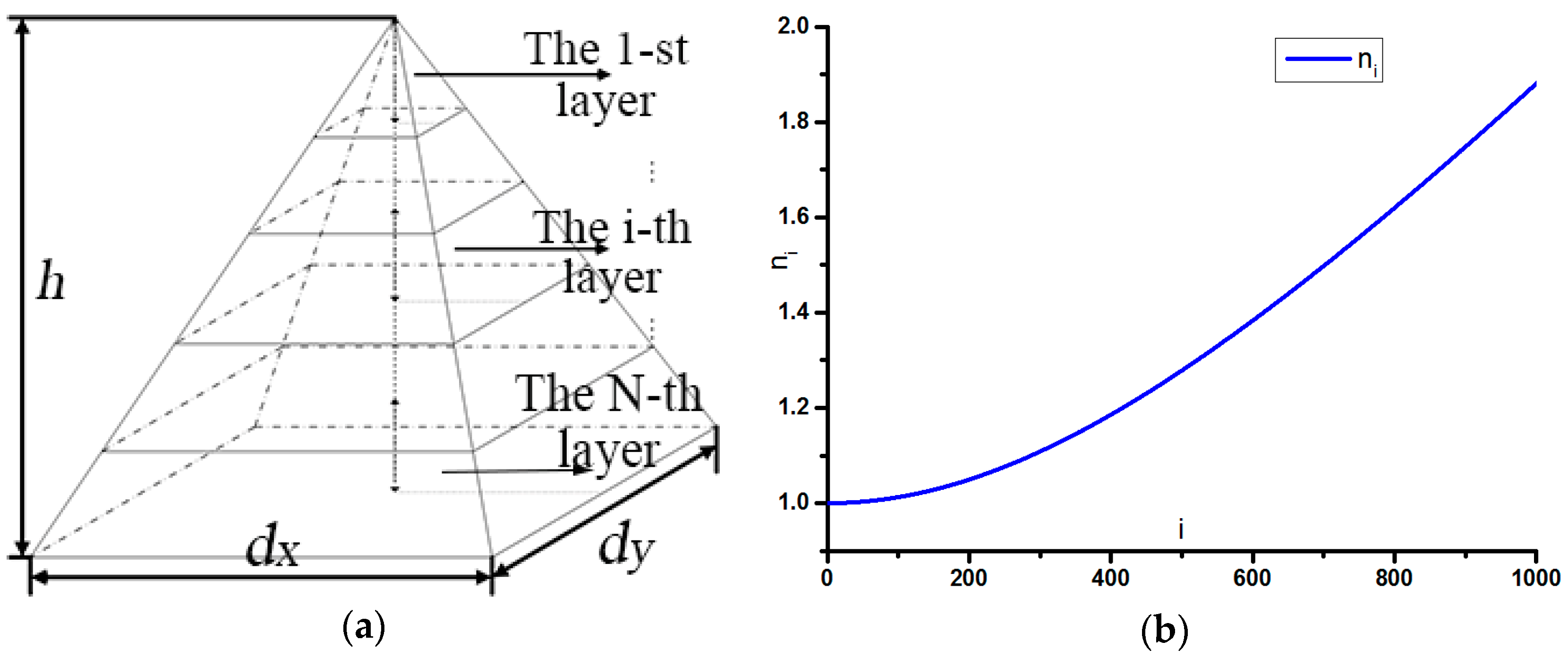
2.1. Modeling Methods

The effect of anti-reflection comes from two aspects: First, the effective refractive index of silicon nitride layer is decreased by the micro-pyramid, which acts as a single-layer anti-reflection film. Second, the localized absorption enhancement is brought by the pyramid structure.
When antireflection properties are realized by patterning the surface with a pyramidal structure, the incoming light perceives this modified region as a thin layer with a certain refractive index, known as the effective refractive index. In this case, the equivalent refractive index gradually increases from the refractive index of air to the refractive index of the absorbing material (silicon nitride, for example). The pyramid structure causes the diminished effective refractive index of silicon nitride, acting as a single-layer antireflection film. Here, three-dimensional vector diffraction theory was used to analyze the influence of the equivalent refractive index on the anti-reflection characteristics [29,30]. The equivalent refractive index can be determined from the grating equation:
n 1 2 sin 2 θ m , n = ( n i sin θ i n cos ϕ + λ m / d x ) 2 + ( n i sin θ i n sin ϕ + λ n / d y ) 2
where n1 is the refractive index on the incident and reflection side, ni is the refractive index of the grating layer, and λ is the wavelength assuming as the interested waveband from 800 to 2500 nm. θm,n, θin, and ϕ are the propagation angle, the angle of incidence and the conical angle, respectively. Furthermore, m and n are the diffraction orders in the x and y directions, respectively, and λ is the wavelength. The dx = dy = d are the micro-pyramid period, and the h is the pyramid height. Additionally, the effective refractive index of the grating layer is decreased by the micro-pyramid, which acts as a single-layer anti-reflection film. Here, the micro-pyramid structure is divided into N layers as shown in Figure 1a. The ni can be calculated by the effective index theory taking into account traditional absorbent materials, as shown in Figure 1b.
With the simulation method of FDTD, the appearance of the reflection suppression with our micro-pyramid array, which enhance the absorption at long wavelengths from 800 to 2500 nm covered the main solar irradiance spectrum, would be observed. Meanwhile, this micro-structure can localize photons and realize the broad-spectrum absorption enhancement inside the micro-pyramid. Figure 2 gives evidence of this light trapping effect by intensity distribution of light field with incoming wave of (a) 800, (b) 1500, and (c) 2100 nm, respectively. Comparing with the absorption inside the substrate, the absorption inside our micro-pyramids is enhanced to almost tripling when the dx = dy = d = 10 μm, and the h = 5 μm. As performed with the FDTD method, it shows that this micro-structure can localize photons and enhance the absorption inside the micro-pyramid.

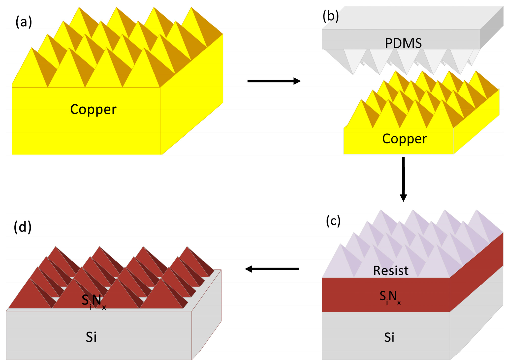
2.2. Fabrication of the Micro-Pyramid Structured Thin Film

There are four main steps of the fabrication process of micro-pyramid structured thin film for broadband infrared antireflection, as shown in Figure 3. Firstly, a pyramid grid was precision machining on a copper mold by the SPDT technique (Figure 3a). Then, the micro-pyramid array was printed in nanoprint resist with NIL (Figure 3b,c) and the final micro-pyramid structures was patterned in SiNx thin film by proportional inductively-coupled plasma etching (ICP) (Figure 3d).
Ultra-precision machining [31] is adopted to precisely fabricate the micro-optical three-dimensional structures. Theory and practice indicates that fly-cutting is extremely suitable for machining repeated complex structures as prism arrays and pyramid arrays with high surface quality and flexibility. In diamond fly-cutting, the tool does not remain in constant contact with the workpiece, it is an interrupted cutting process, which is similar to the single-edge milling. A Cu roller workpiece of 200 mm in diameter is chosen to fix on a workpiece holder which is a vacuum chuck on the rotary B table, while diamond tool is mounted on the spindle C. During fly-cutting, the tool generally rotates and the workpiece remains fixed. An extremely sharpened V-type diamond tool is used to make microgrooves. Figure 4 shows the structural layout of ultra-precision machine tool and on-machine fly-cutting. In order to fabricate the micro-pyramid structure, two V-grooves intersecting at 90° should be prepared. The experimental conditions of fly-cutting is shown in Table 1. A pyramid structure with dimension of 10 μm pitch and 5 μm height has been generated using the SPDT technique (Figure 5a–c).
A 5 μm thick SiNx thin film was deposited on the standard <100>-oriented silicon wafer because of the 5 μm height, 10 μm pitch micro-pyramid array mold chosen for fabrication of antireflective (AR) surfaces. Among the current SiNx layer deposition methods, plasma-enhanced chemical vapor deposition (PECVD) is one of the best, due to the low temperature of the process (usually around 300 °C) and more uniform and less stress variation through wafers. The low deposition temperature of PECVD can alleviate the effects of thermal expansion mismatch, which produces stress between the substrate and coating leading to problem of adhesion. Here, a plasma-enhanced chemical vapor deposition (PECVD) system (SAMCO PD-220, SAMCO, Tokyo, Japan) had been used to investigate some important parameters, such as pressure, power, and gas flow rates. Additionally, introducing this optimized process, a 5.49 μm thick low stress layer was generated, which would be used to patterned micro-pyramid array as presented in the Figure 5d.
Next, the patterned copper mold was coated with anti-adhesive layer and a soft PDMS layer was spun-coated above pyramid texture, and finally covered by a hard, thick PDMS layer. Then this soft composite stamp was demolded from the copper master stamp and coated with anti-sticking layer lowering the surface energy prior to the hot embossing. For the nanoimprint step, a mr-I 7030 R (Micro resist Technology, Berlin, Germany) resist layer was spun onto the SiNx film sample. A hot nanoimprint lithography technique was used to print the micro-pyramid stamp to the resist at 135 °C under 40 bars for 5 min (Figure 5e,f). Due to the low stiffness of the composite mold and micrometer scale of the pyramid shape, the stamp would be printed without deforming in the NIL process.
After cooling the sample, the pyramid structure was obtained in the resist material. Then, this texture was generated on the SiNx layer by using a proportional inductively-coupled plasma (ICP) etching process with sulfur hexafluoride (SF6).
The morphology of the pyramid-SiNx structure were observed by scanning electron microscope (SEM) shown in Figure 5g,h. In addition, atomic force microscopy (AFM, tapping mode, MultiMode 8, Bruker, Madison, WI, USA) could estimate the repeatable uniformity of the surface over the micro-pyramid texture, as shown in Figure 5i. The reflectance of the SiNx thin film with and without the micro-pyramid structures was obtained using an optical spectrometer (PekinElmer Lambda 950 UV/VIS/NIR spectrophotometer with an integrating sphere, 150 mm, PerkinElmer, Inc., Boston, MA, USA) over the wavelength range of 800–2500 nm.

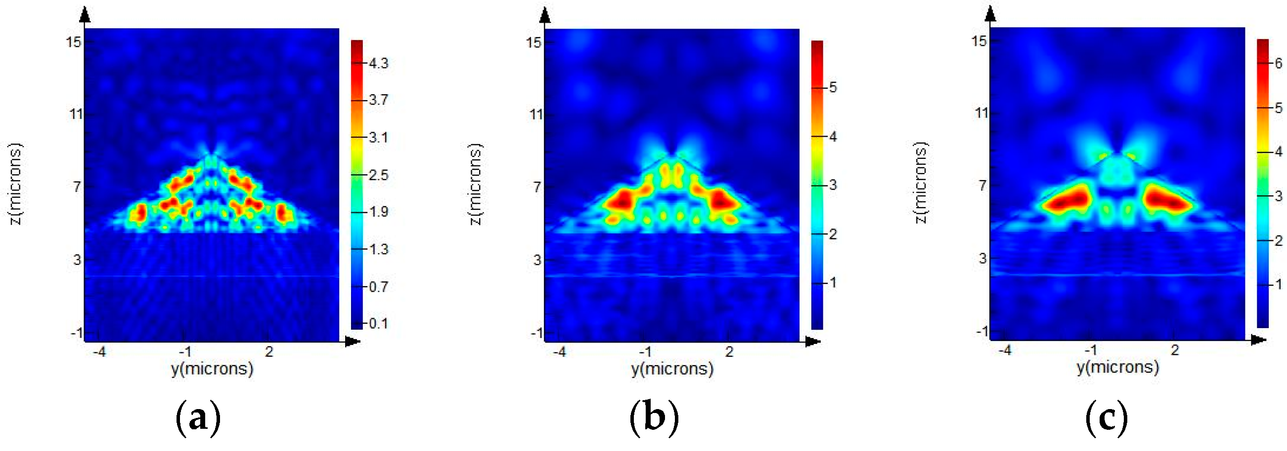
3. Results and Discussion

As described above, a 5 μm height and a 10 μm pitch micro-pyramid array was generated in copper with the SPDT process (Figure 5a–c). A 5.49 μm thick SiNx layer with low stress is produced by the PECVD method (Figure 5d), the micro-pyramid texture was transferred to the nano-imprint resist by using the NIL process (Figure 5e,f), and the final texture was fabricated in the silicon nitride layer by using proportional ICP etching (Figure 5g–i).
According to the simulation results, a pyramid structure with a dimension of 10 μm pitch and 5 μm height represented excellent antireflective performance for the main solar irradiance spectrum (800 to 2500 nm). The effect of anti-reflection comes from the effective refractive index of the silicon nitride layer with the micro-pyramid array and the localized absorption enhancement by the pyramid structure, which is shown by the FDTD analysis.
In the process of fabrication, the pyramid array on the copper mold was generated by the SPDT technique. The area of the micro-structured surface is a circle 12.5 mm in diameter, or a square area 30 mm long and 25 mm wide. It only takes a few minutes to finish the fly-cutting to obtain the pyramid array with a feed rate 500 μm/s. In fact, the size area of the micro-pyramid surface could be generated as large as 300 mm in diameter using the SPDT method. It would take only 20 min to fabricate the pyramid array on the whole surface. There are almost no defects during the fly-cutting, as shown in Figure 5a–c. The pinnacle of the pyramid unit is extremely sharp, and the repeatability of the pyramid shape is high. Compared with the traditional preparation method, the newly-developed method has the advantages of high yield, low cost, large areas, and ease of industrialization. Additionally, the roughness of the surface is pretty good. This means a large area of the structured surface can be directly generated on the plastic film and thin metal film.
As we know by now, using the NIL process can generate the flexible structured surface after fabricating the metal mold. In Figure 5e,f, the micro-pyramid array is replicated well in a large area. The structures on the NIL resist maintain good consistency as the pyramid array on the copper mold.
In order to enhance the localized absorption, the micro-pyramid array should be transferred to the silicon nitride thin film. It turned out to be an effective method to reduce the stress concentration during the deposition of the SiNx layer using PECVD. The SiNx coating is 5.49 μm thick and retains the superior characteristics of low stress and good compactness, as shown in Figure 5d. The micro-pyramids of the SiNx thin film generated by ICP etching were 4 μm in height, which corresponds to a selectivity of 1.25 between the nanoimprint resist and the SiNx coating. Additionally, the side walls of the pyramid are quite smooth after the ICP process. The fabrication of the micro-pyramid-structured dielectric thin film is quite successful in Figure 5g–i.
During the entire fabrication process, a small gap between the micro-pyramid units is formed. Obtaining the texture by SPDT, the flat area is nearly tens of nanometers wide, which has no influence on the pyramid height of 5 μm in the nano-imprint resist before ICP. The proportional ICP process led to the increase of the gap width to more than one hundred nanometers because of the nonlinear feature of the resist.
In Figure 6, the reflectance curves for the 5.5 μm thick SiNx layer and the transferred patterns are measured when the incident light is unpolarized. In the condition of vertical incidence, the reflectance is reduced below 1.0% through the wavelengths concerned.
The effect of anti-reflection comes from two aspects: First, the effective refractive index of silicon nitride layer is decreased by the micro pyramid, which acts as a single-layer anti-reflection film. Second, the localized absorption enhancement is brought by the pyramid structure.
Owing to the excitation of guided resonances, light-trapping can be achieved. The micro-pyramid texture can reduce the front surface reflection and scatter light efficiency into oblique angles. It was generated by a combination of the properties of the relatively low surface area enhancement of about 70% and the gradient refractive index tapered profile. The interface effects in the coating ensure the wave reflected from the antireflection coating top surface to be out-of-phase with that reflected from the semiconductor surface. We consider the interference effect of the reflected light from the interface and how the reflections break there as well.
Furthermore, based on the absorbing material, silicon nitride, the path length of the light would be increasing, by coupling the light into higher diffraction orders. The refraction of light into large angles allows the light to be reflected multiple times, and thereby improves light absorption. It means tapered micro-structures can greatly improve the light absorption over a wide spectral range because of the suppression of reflections and the light-trapping in the long wavelength range. As performed with the FDTD method, it shows that this micro-structure can localize photons and enhance the absorption inside the micro-pyramid.
To summarize, the two influences, a single silicon nitride layer as an anti-reflection film and the micro-pyramid structure analyzed by FDTD, are superimposed together to achieve the final anti-reflection effect. These results show that our structure can realize anti-reflectance efficiently, and this fabrication process is effective with less cost and greater flexibility.

4. Conclusions

In summary, a micro-optical pattern-based optical film, which has a rectangular pyramid shape and a 10 μm pattern size, was designed and fabricated. The patterns were fabricated using the SPDT technique, a hot embossing and ICP etching process. Compared to the wet-patterning approach, we can generate an angle-tunable pyramid structure. Micro-pyramid structures in the silicon nitride thin film are resistant to high temperatures, acid corrosion, and have better adhesion compared to polymer coatings. An optical property of reflectivity, less than 1.0%, was achieved by our approach. Thus, proving that large-scale pyramid structures are effective for antireflection in broadband wavelengths.
Moreover, the performance of antireflection is analyzed by simulating the micro-pyramid structures by the FDTD method. This low reflectance is associated to light trapping and multiple reflections in the very sharp pyramid shape manufactured within the silicon nitride layer. Our results show that the interference effect of thin films and the pyramid structures are beneficial to the light-trapping effect.

Author Contributions

S.G. and W.L. conceived and designed the experiments; S.G., S.Z., S.L., and Y.H. performed the experiments; S.G., W.L., X.S., and P.Y. analyzed the data; J.Z. and D.L. contributed analysis tools; and S.G. and W.L. wrote the paper.

Funding

This research was supported by the National Basic Research Project (JCKY2016208A002), Advanced Manufacturing Project (41423020111), the National Natural Science Foundation of China (no. 61505157), the National Natural Science Foundation of China (no. 51502232), Scientific Research Plan Projects of Shaanxi Education Department (16JK1363), and the National R and D Program of China (2017YFA0207400), the principal fund of Xi’an Technological University (no. 302021501).

Conflicts of Interest

The authors declare no conflict of interest.

References

  1. Heavens, O.S. Thin-film optical filters. Opt. Acta Int. J. Opt. 2010, 33, 1336. [Google Scholar] [CrossRef]
  2. Atwater, H.A.; Polman, A. Plasmonics for improved photovoltaic devices. Nat. Mater. 2010, 9, 205–213. [Google Scholar] [CrossRef] [PubMed]
  3. Graetzel, M.; Janssen, R.A.; Mitzi, D.B.; Sargent, E.H. Materials interface engineering for solution-processed photovoltaics. Nature 2012, 488, 304–312. [Google Scholar] [CrossRef] [PubMed]
  4. Franklin, E.; Fong, K.; Mcintosh, K.; Fell, A.; Blakers, A.; Kho, T.; Walter, D.; Wang, D.; Zin, N.; Stocks, M. Design, fabrication and characterisation of a 24.4% efficient interdigitated back contact solar cell. Prog. Photovolt. Res. Appl. 2016, 24, 411–427. [Google Scholar] [CrossRef]
  5. Wilson, S.J.; Hutley, M.C. The optical properties of “moth eye” antireflection surfaces. Opt. Acta Int. J. Opt. 1982, 29, 993–1009. [Google Scholar] [CrossRef]
  6. Clapham, P.B.; Hutley, M.C. Reduction of lens reflexion by the “moth eye” principle. Nature 1973, 244, 281–282. [Google Scholar] [CrossRef]
  7. Paivanranta, B.; Saastamoinen, T.; Kuittinen, M. A wide-angle antireflection surface for the visible spectrum. Nanotechnology 2009, 20, 375301. [Google Scholar] [CrossRef] [PubMed]
  8. Amalathas, A.P.; Alkaisi, M.M. Efficient light trapping nanopyramid structures for solar cells patterned using uv nanoimprint lithography. Mater. Sci. Semicond. Process. 2017, 57, 54–58. [Google Scholar] [CrossRef]
  9. Alshal, M.A.; Allam, N.K. Broadband absorption enhancement in thin film solar cells using asymmetric double-sided pyramid gratings. J. Electron. Mater. 2016, 45, 5685–5694. [Google Scholar] [CrossRef]
  10. Chong, T.K.; Wilson, J.; Mokkapati, S.; Catchpole, K.R. Optimal wavelength scale diffraction gratings for light trapping in solar cells. J. Opt. 2012, 14, 024012. [Google Scholar] [CrossRef]
  11. Mavrokefalos, A.; Han, S.E.; Yerci, S.; Branham, M.S.; Chen, G. Efficient light trapping in inverted nanopyramid thin crystalline silicon membranes for solar cell applications. Nano Lett. 2012, 12, 2792–2796. [Google Scholar] [CrossRef] [PubMed]
  12. Zhao, J.; Wang, A.; Green, M.A.; Ferrazza, F. 19.8% efficient “honeycomb” textured multicrystalline and 24.4% monocrystalline silicon solar cells. Appl. Phys. Lett. 1998, 73, 1991–1993. [Google Scholar] [CrossRef]
  13. Sivasubramaniam, S.; Alkaisi, M.M. Inverted nanopyramid texturing for silicon solar cells using interference lithography. Microelectron. Eng. 2014, 119, 146–150. [Google Scholar] [CrossRef]
  14. Jiang, W.; Liu, H.Z.; Yin, L.; Shi, Y.S.; Chen, B.D. Enhanced photoelectric properties in dye-sensitized solar cells using TiO2 pyramid arrays. J. Phys. Chem. C 2016, 120, 9678–9684. [Google Scholar] [CrossRef]
  15. Yu, Z.; Gao, H.; Wu, W.; Ge, H.; Chou, S.Y. Fabrication of large area subwavelength antireflection structures on si using trilayer resist nanoimprint lithography and liftoff. J. Vac. Sci. Technol. B 2003, 21, 2874–2877. [Google Scholar] [CrossRef]
  16. Wang, Z.H.; Liu, W.; Zuo, Q. Application of lift-off process in fabricating nanoimprint stamp. Adv. Mater. Res. 2014, 924, 359–365. [Google Scholar] [CrossRef]
  17. Woo, J.C.; Baek, N.S.; Joo, B.; Kim, Y.; Kim, C.I.; Woo, J.C.; Joo, B.; Kim, C.I. The periodically negative semi-pyramid nanostructured polymer layer for broadband anti-reflection effect. RSC Adv. 2012, 2, 7677–7680. [Google Scholar] [CrossRef]
  18. Lin, J.S.; Chu, W.P.; Juang, F.S.; Chen, N.P.; Tsai, Y.S.; Chen, C.C.; Chen, C.M.; Liu, L.C. Manufacture of light-trapping (LT) films by ultraviolet (Uv) irradiation and their applications for polymer solar cells (PSCS). Mater. Lett. 2012, 67, 42–45. [Google Scholar] [CrossRef]
  19. Lee, Y.C.; Ni, C.H.; Chen, C.Y. Enhancing light extraction mechanisms of GaN-based light-emitting diodes through the integration of imprinting microstructures, patterned sapphire substrates, and surface roughness. Opt. Express 2010, 18, A489–A498. [Google Scholar] [CrossRef] [PubMed]
  20. Mohamed, K.; Alkaisi, M.M.; Blaikie, R.J. The replication of three dimensional structures using uv curable nanoimprint lithography. J. Vac. Sci. Technol. B 2008, 26, 2500–2503. [Google Scholar] [CrossRef]
  21. Park, J.-W.; Lee, J.-G.; Shim, G.-S.; Kim, H.-J.; Kim, Y.-K.; Moon, S.-E.; No, D.-H. Evaluation of the ultraviolet-curing kinetics of ultraviolet-polymerized oligomers cured using poly (ethylene glycol) dimethacrylate. Coatings 2018, 8, 99. [Google Scholar] [CrossRef]
  22. Päivänranta, B.; Heikkilä, N.; Kuittinen, M. Antireflective subwavelength-structured surfaces with enhanced color properties. J. Opt. Soc. Am. A 2007, 24, 1680–1686. [Google Scholar] [CrossRef]
  23. Dongxu, W.; Guo, L.; Bo, W.; Zheng, Q.; Lei, L. Fabrication of microstructured surfaces by five-axis ultra precision machine tool. Key Eng. Mater. 2015, 625, 187–191. [Google Scholar]
  24. Chao, C.L.; Lin, W.C.; Chou, W.C.; Ko, J.L.; Ma, K.J.; Chao, C.W. Study on fabricating of micro-pyramid array by precision diamond turning. In Proceedings of the International Conference on Optics in Precision Engineering and Nanotechnology (icOPEN2013), Singapore, 9–11 April 2013; Volume 8769, 87691C. [Google Scholar] [CrossRef]
  25. Xie, J.; Zhuo, Y.W.; Tan, T.W. Experimental study on fabrication and evaluation of micro pyramid-structured silicon surface using a V-tip of diamond grinding wheel. Precis. Eng. 2011, 35, 173–182. [Google Scholar] [CrossRef]
  26. Park, S.; Lee, S.-K. Micro-optical pattern-based selective transmission mechanism. Appl. Opt. 2016, 55, 2457–2462. [Google Scholar] [CrossRef] [PubMed]
  27. Villanueva, L.; Vazquez-Mena, O.; Martin-Olmos, C.; Savu, V.; Sidler, K.; Brugger, J. Resistless fabrication of nanoimprint lithography (NIL) stamps using nano-stencil lithography. Micromachines 2013, 4, 370–377. [Google Scholar] [CrossRef]
  28. Nagato, K. Injection compression molding of replica molds for nanoimprint lithography. Polymers 2014, 6, 604–612. [Google Scholar] [CrossRef]
  29. Li, L. Note on the s-matrix propagation algorithm. J. Opt. Soc. Am. A 2003, 20, 655–660. [Google Scholar] [CrossRef]
  30. Granet, G.; Plumey, J. Parametric formulation of the fourier modal method for crossed surface-relief gratings. J. Opt. A Pure Appl. Opt. 2002, 4, S145. [Google Scholar] [CrossRef]
  31. Zhao, C.; Cheung, C.; Liu, M. Modeling and simulation of a machining process chain for the precision manufacture of polar microstructure. Micromachines 2017, 8, 345. [Google Scholar] [CrossRef]
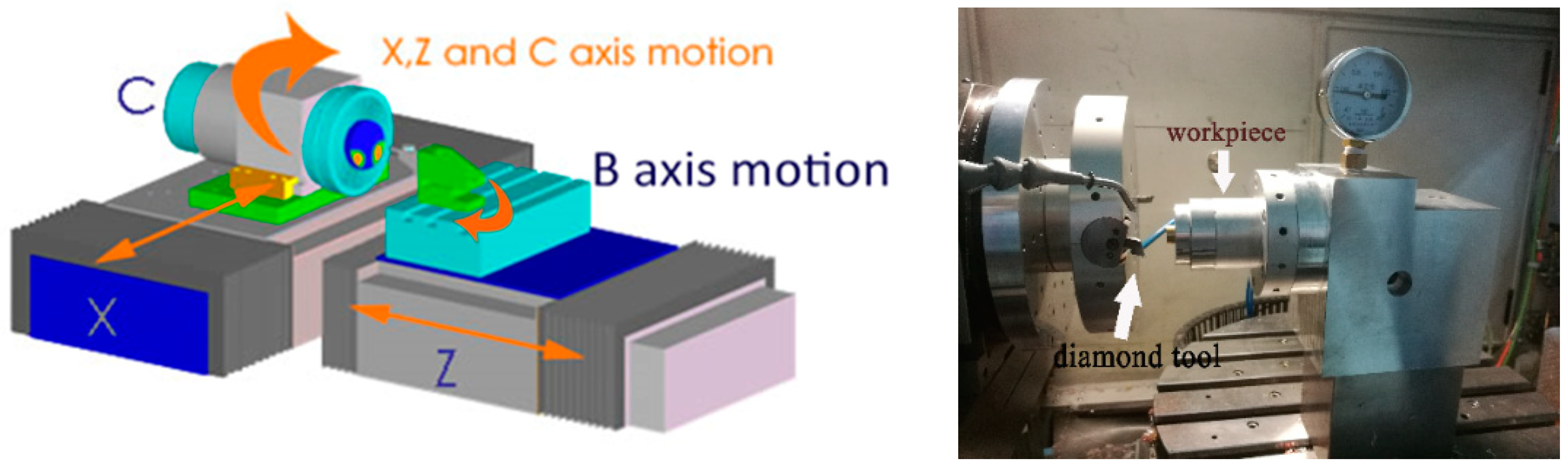
Figure 1. The modeling methods (a) and ni (b).
Coatings 08 00192 g001
Figure 2. Photon absorption profile at cross section at (a) 800 nm; (b) 1500 nm; and (c) 2100 nm wavelength.
Coatings 08 00192 g002
Figure 3. Preparation of micro-pyramid structured thin film for broadband infrared antireflection. (a) Firstly, the micro-pyramid array is generated on a copper mold by the SPDT technique; (b) Next, a soft composite PDMS (Polydimethylsiloxane) stamp was demolded from the copper master stamp; (c) Then, a nano-imprint lithography resist is spun onto a silicon nitride layer and the micro-pyramid array is copied into resist by using the PDMS stamp; (d) The pattern is transferred to the silicon nitride thin film by proportional inductively-coupled plasma etching.
Coatings 08 00192 g003
Figure 4. Structural layout of ultra-precision machine tool and on-machine fly-cutting.
Coatings 08 00192 g004
Figure 5. SEM images and AFM images of the samples with the micro-pyramids texture. (ac) An array of micro-pyramids is obtained with the SPDT process; (d) a 5.49 μm thick SiNx layer with low stress is produced by the PECVD method; (e,f) a micro-pyramid grid in the NIL resist is obtained and (gi) a final micro-pyramid texture in the SiNx film is generated.
Coatings 08 00192 g005
Figure 6. Reflectance curves for 5.49 μm thick SiNx layers and the measured micro-pyramid array.
Coatings 08 00192 g006
Table 1. The experimental conditions of fly-cutting.
WorkpieceTool Included Angle (°)Depth of Cut (μm)Feed Rate (μm/s)Spindle Rotational Speed (rpm)
Copper alloy9055003000

