A Ladder-Type Organosilicate Copolymer Gate Dielectric Materials for Organic Thin-Film Transistors

Department of Chemical and Biomolecular Engineering, Sogang University, Seoul 04107, Korea
*
Author to whom correspondence should be addressed.
Coatings 2018, 8(7), 236; https://doi.org/10.3390/coatings8070236
Submission received: 31 May 2018
/
Revised: 27 June 2018
/
Accepted: 2 July 2018
/
Published: 3 July 2018
(This article belongs to the Special Issue Active Organic and Organic-Inorganic Hybrid Coatings and Thin Films: Challenges, Developments, Perspectives)
Abstract
:A ladder-type organosilicate copolymer based on trimethoxymethylsilane (MTMS) and 1,2-bis(triethoxysilyl)alkane (BTESn: n = 2–4) were synthesized for use as gate dielectrics in organic thin-film transistors (OTFTs). For the BTESn, the number of carbon chains (2–4) was varied to elucidate the relationship between the chemical structure of the monomer and the resulting dielectric properties. The developed copolymer films require a low curing temperature (≈150 °C) and exhibit good insulating properties (leakage current density of ≈10−8–10−7 A·cm−2 at 1 MV·cm−1). Copolymer films were employed as dielectric materials for use in top-contact/bottom-gate organic thin-film transistors and the resulting devices exhibited decent electrical performance for both p- and n-channel organic semiconductors with mobility as high as 0.15 cm2·V−1·s−1 and an Ion/Ioff of >105. Furthermore, dielectric films were used for the fabrication of TFTs on flexible substrates.
1. Introduction
Organic thin-film transistors (OTFTs) have been an important research subject because they are indispensable elements in the development of low-cost, large-area electronics, such as paper-based displays, smart cards, radio-frequency ID tags, and sensors [1,2,3,4,5,6,7,8]. Among the fundamental components of OTFTs, namely the semiconductor, dielectric, and conductor, studies on the development and application of organic semiconducting materials have intensively been performed for the last few decades [9,10,11,12,13,14,15,16,17,18]. Development of new dielectric materials for OTFTs, which perform as capacitors, insulators, and substrates, is also important to realize various electronic applications based on OTFTs. Favorable dielectric characteristics of OTFT-based electronic devices include ease of preparation, low cost, large area processibility, as well as excellent insulating properties [19,20,21,22,23].
Inorganic materials, such as SiO2, Al2O3, and TiO2, have traditionally been employed as dielectrics for OTFTs due to their excellent insulating properties. However, inorganic dielectric materials require a high-temperature/high-cost vacuum process for their preparation [24,25]. On the other hand, organic dielectric materials, such as polymers, can readily be processed from solution at a relatively low temperature over a large area, while their insulating properties are inferior to those of inorganic counterparts [26,27,28]. Furthermore, some organic-based dielectrics can be readily processed at low temperature, which can be employed on flexible substrates, such as polyethylene terephthalate (PET) and polyethylene naphthalate (PEN) [29,30,31,32,33,34,35,36,37,38].
To this end, many studies on the development and application of new dielectric materials with low leakage current, high dielectric constant, and facile process have been reported [39,40,41,42,43,44,45,46,47,48]. Among them, organic-inorganic hybrid dielectrics might synergistically combine the advantages of both materials, i.e., the excellent mechanical and electrical properties of inorganics and the flexibility and large area solution processibility of organics [41,42,43,44]. One of the representative examples is organosilicate materials, a type of silica containing organic groups. A few studies employing dielectric materials containing organosilicates have been reported for the fabrication of OTFTs [45,46,47,48].
For instance, Kang et al. reported silsesquioxane copolymer gate dielectrics based on methacryloxy propyltrimethoxysilane and phenyltrimethoxysilane for use in OTFTs. The reported dielectric films formed at a curing temperature of 200 °C exhibited a leakage current density as low as 6 × 10⁻⁹ A·cm−2 at 1 MV·cm−1 [45]. Similarly, Kim et al. reported dielectric materials based on a silsesquioxane derivative containing cage-structured epoxy groups, and the resulting films showed a leakage current density of ≈10−8 A·cm−2 at 1 MV·cm−1 [46]. Lee et al. reported hybrid copolymer gate dielectrics based on methyltrimethoxysilane and 1,2-bis(trimethoxysilyl)ethane for use in OTFTs, with a leakage current density of 2.9 × 10⁻⁶ A·cm−2 at 0.5 MV·cm−1 [47]. Similarly, Hamada et al. reported on a polymethylsilsesquioxane (PMSQ) dielectric prepared by a sol-gel method from methyltrimethoxysilane. While the dielectric characteristic (leakage current density) was not reported in this study, the OTFTs based on the PMSQ dielectric showed very poor electrical performance with a mobility of ≈ 0.006 cm2·V−1·s−1 [48].
In this study, we report a ladder-type copolymer based on trimethoxymethylsilane (MTMS) and 1,2-bis(triethoxysilyl)alkane (BTESn) as dielectric materials. Previously reported organosilicate copolymer dielectric films based on similar monomers exhibited high leakage current density, resulting in relatively poor device characteristic for poly(3-hexylthiophene) (P3HT), possibly due to the unoptimized processing conditions [47]. Hence, we have optimized the synthesis and processing condition of copolymers by varying the monomer ratio, solvent, and employing different types of monomers. The copolymers were synthesized by a simple sol-gel reaction of two types of monomers, and curing was performed at a relatively low annealing temperature of 150 °C. The resulting films exhibited a leakage current density of 10−8–10−7 A·cm−2 at 1 MV·cm−1 at a thickness of ≈100 nm. Furthermore, the correlation between the dielectric properties of the copolymers and types of monomers was investigated by varying carbon chain lengths in BTESn. The OTFTs employing copolymer dielectrics were fabricated, and the resulting devices were active for both p- and n-channel organic semiconductors with carrier mobility as high as 0.15 cm2 V−1·s−1 and a current on/off ratio of ≈105 (Figure 1). Furthermore, we have employed the developed copolymer dielectric films on flexible substrate to fabricate flexible TFTs.
2. Materials and Methods
2.1. Materials and Methods
The semiconductors pentacene (P5) and N,N′-Dioctyl-3,4,9,10-perylenedicarboximide (PTCDI-C13) were purchased from Sigma-Aldrich (St. Louis, MO, USA). Trimethoxymethylsilane (MTMS) and 1,2-bis(triethoxysilyl) ethane (BTES2), 1,2-bis(triethoxysilyl) propane (BTES3), 1,2-bis(triethoxysilyl) butane (BTES4) were purchased from Sigma-Aldrich (St. Louis, MO, USA). All materials were used without further purification. PEN substrates (Film Type Teonex Q65H, DuPont Teijin Films, Chester, VA, USA) were used as received without solvent cleaning. Structures of the MTMS-BTESn were studied by 1H NMR spectroscopy (Varian UNITY-INOVA 500 MHz NMR spectrometer using Acetone-d6 as a solvent, Palo Alto, CA, USA) and Fourier transform infrared spectroscopy (FT-IR, Thermo Scientific Nicolet iS50R FTIR Spectrometer, Thermo Fisher Scientific, Waltham, MA, USA). Thermogravimetric analyses (TGA, TA Instrument Q50-1555, New Castle, DE, USA) were performed on each sample in a platinum crucible from 40 to 800 °C at a heating rate of 10 °C min−1 under an N2 atmosphere.
2.2. Synthesis
2.2.1. Synthesis of MTMS-BTES2
Trimethoxymethylsilane (5.11 g, 37.5 mmol) and 1,2-bis (triethoxysilyl) ethane (4.43 g, 12.5 mmol) were added to anhydrous tetrahydrofuran (25 mL) and stirred at room temperature for 30 min. To this solution was added a 2N aqueous hydrochloric acid solution (0.75 mL) and distilled water (8.32 mL), and the mixture was stirred at 40 °C for 6 h under a nitrogen atmosphere to perform a sol-gel reaction. The reaction mixture was cooled to room temperature, and the organosilicate precursor synthesized from the solution was extracted with diethyl ether (50 mL). The extracted precursor solution was washed twice with distilled water, and then dried under vacuum at room temperature for 1 h to remove the solvent to obtain a white powdery solid. The solids were again dissolved in acetone (200 mL) to afford the gelation of the organosilicate, and undissolved particles were removed by filtration. The solution was dried under vacuum at room temperature for 12 h using a rotary evaporator to remove residual solvent, and a white solid (3.97 g, 41.61%) was obtained again. 1H-NMR (500 MHz, Acetone-d6): δ 0.19 (s, 3H), 0.90 (s, 2H), 5.70 (s, H).
2.2.2. Synthesis of MTMS-BTES3
Trimethoxymethylsilane (5.11 g, 37.5 mmol) and 1,2-bis (triethoxysilyl) propane (4.61 g, 12.5 mmol) were added to anhydrous tetrahydrofuran (25 mL) and stirred at room temperature for 30 min. To this solution was added a 2N aqueous hydrochloric acid solution (0.75 mL) and distilled water (8.32 mL), and the mixture was stirred at 40 °C for 6 h under a nitrogen atmosphere to perform a sol-gel reaction. The next purification processes were same as those of MTMS-BTES2 and a white solid (4.43 g, 45.58%) was obtained. 1H-NMR (500 MHz, Acetone-d6): δ 0.19 (s, 3H), 0.90 (s, 2H), 1.71 (s, 2H), 5.70 (s, H).
2.2.3. Synthesis of MTMS-BTES4
Trimethoxymethylsilane (5.11 g, 37.5 mmol) and 1,2-bis (triethoxysilyl) butane (4.78 g, 12.5 mmol) were added to anhydrous tetrahydrofuran (25 mL) and stirred at room temperature for 30 min. To this solution was added a 2N aqueous hydrochloric acid solution (0.75 mL) and distilled water (8.32 mL), and the mixture was stirred at 40 °C for 6 h under a nitrogen atmosphere to perform a sol-gel reaction. The next purification processes were same as those of MTMS-BTES2 and a white solid (4.68 g, 47.32%) was obtained. 1H-NMR (500MHz, Acetone-d6): δ 0.19 (s, 3H), 0.90 (s, 2H), 1.71 (s, 2H), 5.70 (s, H).
2.3. Film Preparation and Device Fabrication
Top-contact/bottom-gate organic thin-film transistor devices were fabricated using highly n-doped silicon wafers (resistivity < 0.005 Ω∙cm) as gate/substrates. The substrates were cleaned by sonication in isopropyl alcohol for 20 min, followed by O2 plasma for 5 min (Harrick Plasma, 18W, Ithaca, NY, USA). For the fabrication of devices on flexible substrates, the bottom Al gate electrodes were thermally evaporated through a shadow mask on the polyethylene naphthalate (PEN) substrate. For the preparation of a gate dielectric layer, MTMS-BTESn (n = 2–4) was dissolved in propylene glycol monomethyl ether acetate (PGMEA) solvent at 10 wt.%. The resulting solutions were dropped on a silicon wafer or PEN substrates with Al gate electrodes through a syringe equipped with a 0.2 μm polytetrafluoroethylene (PTFE) filter, and then spun at 3000 rpm for 30 s. The spin-coated films were annealed at 150 °C for 2 h under nitrogen. Film thicknesses were 80–150 nm, as characterized by an ellipsometer. A 40 nm thick P5 or PTCDI-C13 film was deposited onto the prepared MTMS-BTESn copolymer gate dielectrics at a rate of 0.2 Å·s−1 (≈10−5 Torr). Finally, a gold source and drain electrode (40 nm) was thermally evaporated through a shadow mask with channel lengths (L, 50–100 μm) and width (W, 1000–2000 μm).
Metal/insulator/semiconductor (MIS) structures were fabricated using highly n-doped silicon wafers as a gate/substrate. Then the organosilicate copolymer dielectric was spin-coated and annealed at 150 °C for 2 h, as described above. Finally, gold top electrodes (40 nm) were thermally deposited. The area of the testing capacitor was 0.2 mm × 0.2 mm.
2.4. Film and Device Characterization
Film thicknesses were characterized by ellipsometer (Filmetrics, F20, San Diego, CA, USA). The surface morphologies of copolymer thin films were characterized by atomic force microscope (AFM, NX10, Park Systems, Suwon, South Korea). A Keithley 4200 SCS (Cleveland, OH, USA) was used for the characterization of OTFTs and leakage current measurements. The capacitance measurement of copolymer thin films were performed using an LCR meter (Agilent 4284A, Agilent Technologies, Santa Clara, CA, USA). Carrier mobilities (μ) were determined in the saturation regime using the standard relationship, μsat = (2IDSL)/[WCi(VG − VT)2] (IDS, source-drain current; L, the channel length; W, channel width; Ci, areal capacitance of the gate dielectric; VG, gate voltage; VT, threshold voltage).
3. Results
3.1. Synthesis
MTMS-BTESn copolymers were prepared using a sol-gel reaction of MTMS and BTESn, and were characterized by 1H-NMR and FT-IR (Figures S1 and S2). As shown in the NMR spectra (Figure S1), the MTMS monomer was confirmed by the pendant methyl group peak at ≈0.08–0.2 ppm. The BTESn monomer was confirmed by ethylene bridge structure peak formed at 0.8 ppm. BTES3 and BTES4 were additionally confirmed at ≈1.6 ppm using a bridge structure peak. Note that the peak at ≈6 ppm is from the residual hydroxide group formed during the polymerization. The network structure formed between MTMS and BTESn can be confirmed by FT-IR spectra (Figure S2). Two absorption peaks at 1131 and 1040 cm−1, corresponding to Si–O–Si stretching vibrations, were observed in all samples. The bimodal absorption peaks indicate the formation of ladder-type structures [49,50,51].
3.2. Dielectric Characterization
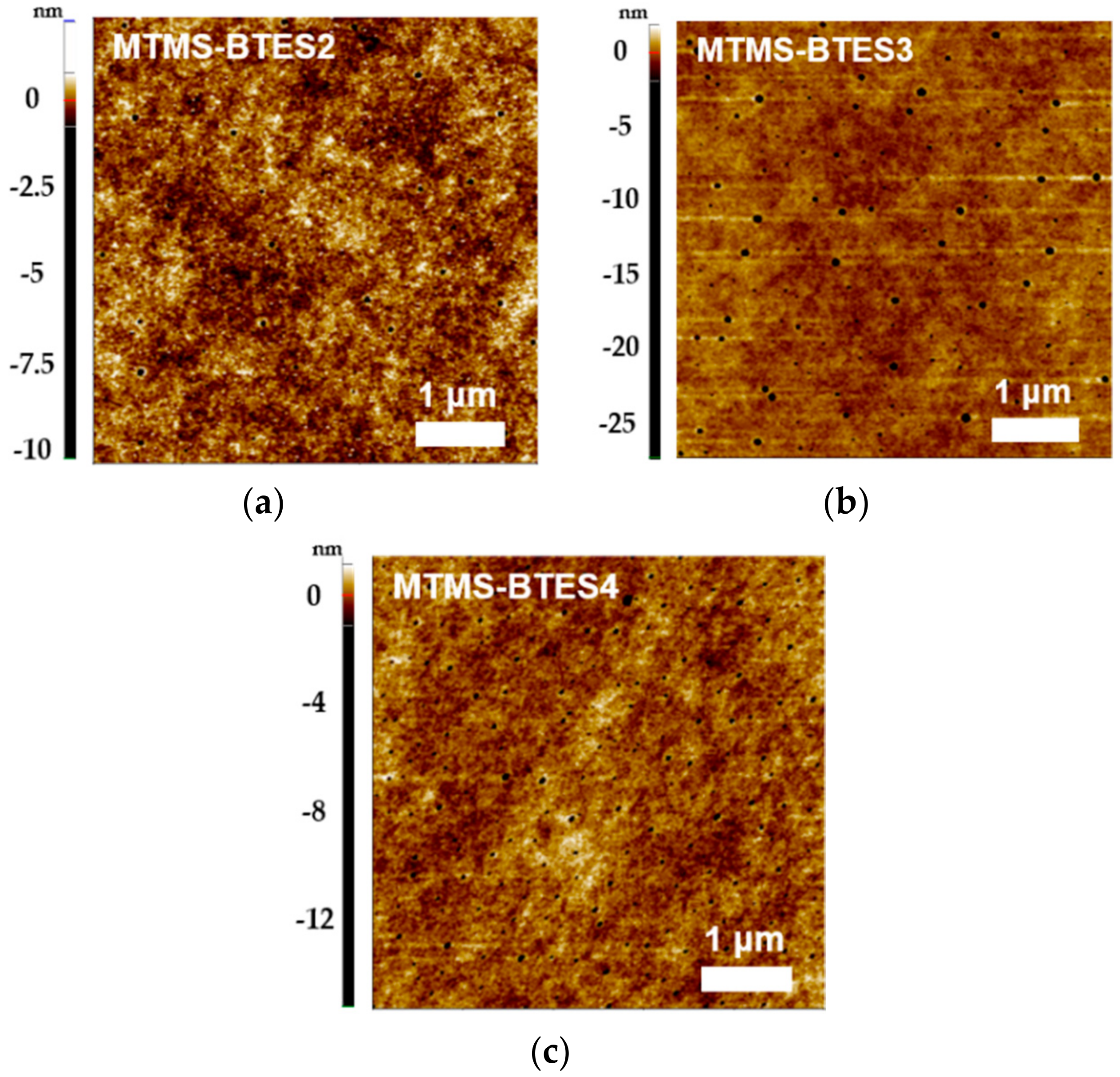
The MTMS-BTESn copolymer film was formed via spin-coating onto a substrate to a thickness of ≈80–150 nm, as measured by an ellipsometer. First, the surface morphologies of the dielectric films were characterized using an AFM, and a relatively smooth surface (root-mean-square roughness: 0.4–1.0 nm) was observed, regardless of the film thickness (Figure 2).
Then, the leakage current density and areal capacitance of the dielectric films were measured based on the MIS structure with Au top electrodes (Table 1 and Figure 3). First, all dielectric films showed a low leakage current density of ≈10−8–10−7 A·cm−2 at 1 MV·cm−1 (Figure 3a). Although there was no significant difference with regard to the type of monomer, the leakage current density slightly increased as the number of carbon atoms of BTESn increased (Figure 3c). The methyl groups in the MTMS might reduce the relative amount of hydroxyl groups during the sol-gel reaction and increase the stability of the film [37]. Also, electrical stability of the dielectric can be enhanced by reducing the free volume due to the low curing temperature of 150 °C and by limiting the thermal dynamic motion of the polymer chains due to the sol-gel bonded network structure.
In the case of the capacitance measurement, the measurement was performed between 10 and 103 kHz. As the frequency increased, the capacitance value decreased slightly. Based on the capacitance value at 102 kHz, the dielectric constants were 3.3–3.5, which is similar to the conventional organosilicate-based materials [35,36,37]. For the dielectric films with comparable thickness, as the number of carbon in the monomers increased, the value of k decreased, which could be a result of the increased free volume of monomers with more carbon chains.
3.3. Thin-Film Transistor Fabrication and Characterization
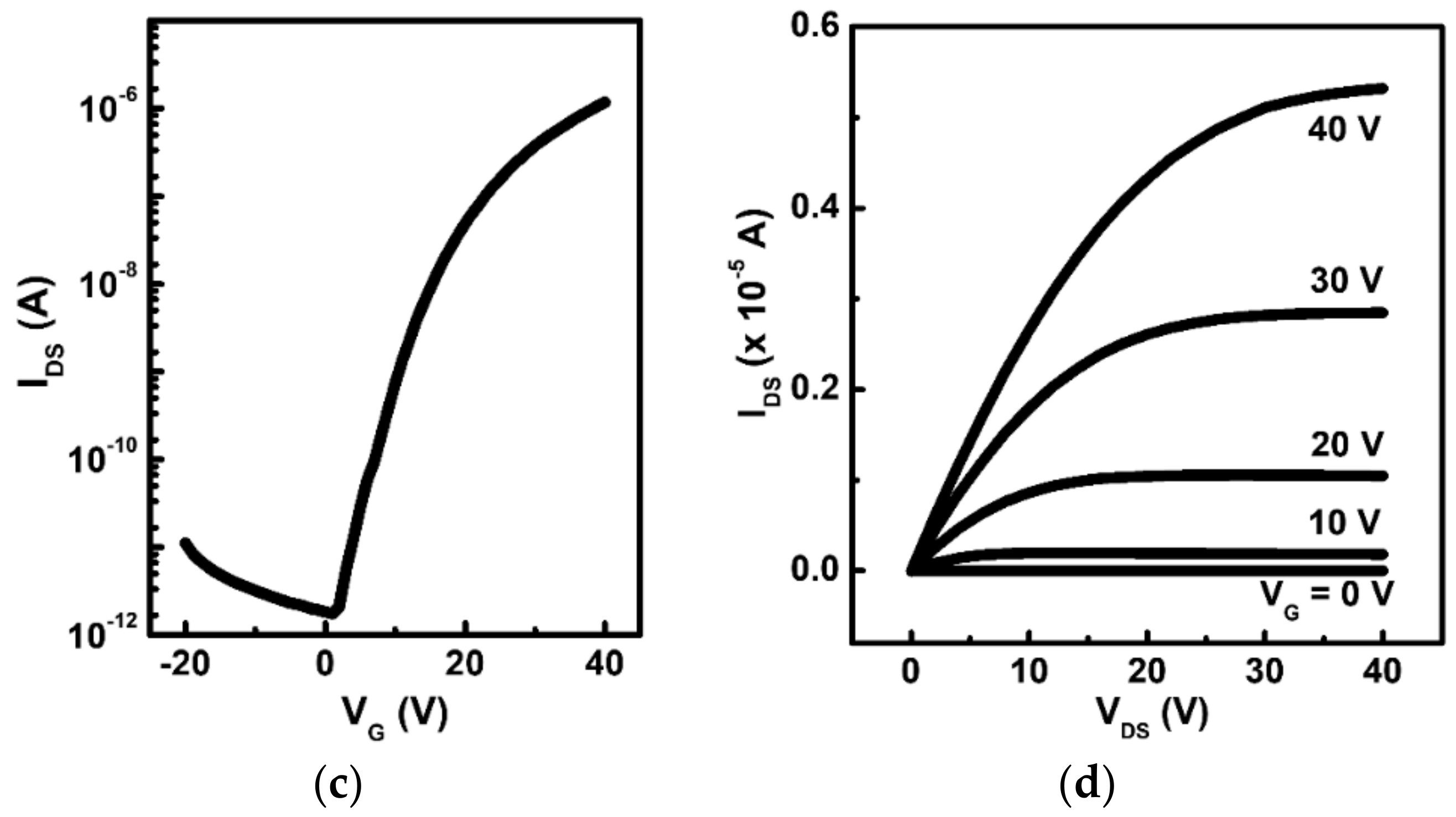
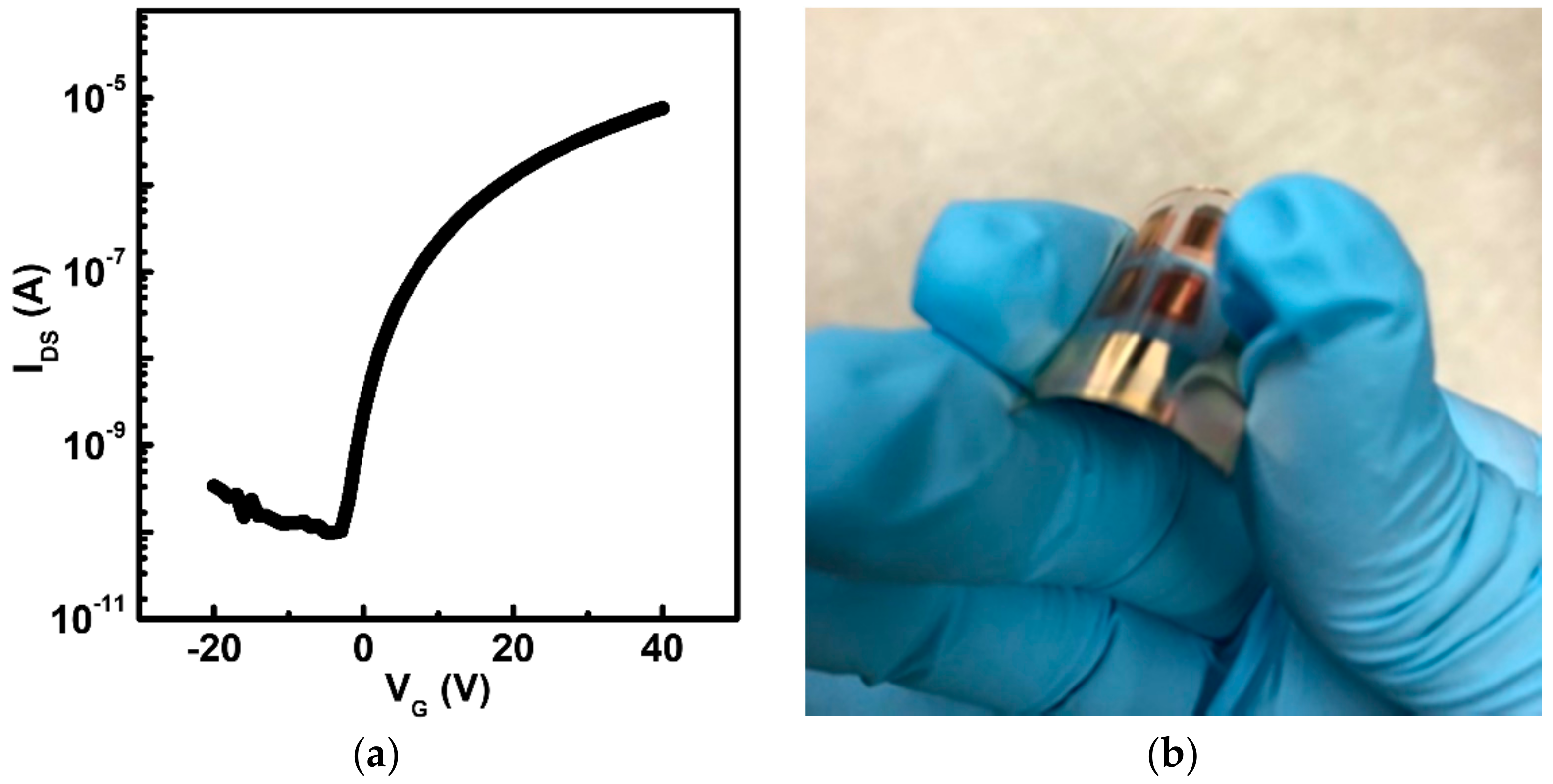
We fabricated OTFTs by spin-coating MTMS-BTESn materials on the n++-Si gate/substrate, followed by annealing at 150 °C for 2 h. P-type (P5) and n-type (PTCDI-C13) organic semiconductors were vacuum-deposited onto the copolymer dielectric layer, followed by Au source/drain electrodes. The device characteristics including carrier mobilities in the saturation regime (μsat), and current on/off ratios (Ion/Ioff), and threshold voltage (VT) are shown in Table 2. Transfer characteristics of the devices were measured in the saturation regime (VDS ≥ VG − VT), and representative transfer plots are shown in Figure 4. As shown, the OTFT devices operated well for both p- and n-channel organic semiconductors with a carrier mobility as high as 0.15 cm2·V−1·s−1 and Ion/Ioff of >105. Furthermore, copolymer dielectric films could be employed on flexible PEN substrates, due to the low curing temperature, and the resulting OTFT device showed a slightly lower performance than that on a rigid substrate with an electron mobility of 0.04 cm2·V−1·s−1 for the PTCDI-C13 semiconductor (Figure 5).
4. Conclusions
This article explored the dielectric characteristics of a copolymer based on MTMS and BTESn with various carbon numbers. Organosilicate copolymer dielectrics with various lengths of carbon chains could be easily prepared by the sol-gel method. Despite the existence of natural free volume due to the difference of compatibility between organic and inorganic materials, a good insulating property of copolymer dielectrics was observed. All three types of dielectric films exhibited a relatively smooth surface and low leakage current density of ≈10−8–10−7 A·cm−2 at 1 MV·cm−1 via the optimization of processing conditions and monomer components. With regard to different chemical structure of monomers, the leakage current density increased slightly, while dielectric constant value decreased, as the number of carbon atoms in BTESn increased, possibly due to the structural free volume caused by the carbon bridge. The copolymer films were employed as a dielectric layer for OTFTs, and the resulting devices were active for both p- and n-channel organic semiconductors with a carrier mobility as high as 0.15 cm2·V−1·s−1 and Ion/Ioff of ≈ 105.
Supplementary Materials
The following are available online at https://www.mdpi.com/2079-6412/8/7/236/s1, Figure S1: 1H-NMR analysis of MTMS-BTESn copolymer, Figure S2: Fourier transform infrared spectroscopy (FT-ir) of MTMS-BTESn copolymer
Author Contributions
D.K. and C.K. designed the experiments. D.K. performed the experiments. D.K. and C.K. wrote the paper.
Funding
This research was funded by the National Research Foundation of Korea (NRF) (NRF-2017R1A2B4001955 and NRF-2017M2B2A4049297).
Conflicts of Interest
The authors declare no conflict of interest.
References
- Ortiz, R.P.; Facchetti, A.; Marks, T.J. High-k Organic, Inorganic, and Hybrid Dielectrics for Low-Voltage Organic Field-Effect Transistors. Chem. Rev. 2010, 110, 205–239. [Google Scholar] [CrossRef] [PubMed]
- Kang, B.S.; Lee, W.H.; Cho, K.W. Recent Advances in Organic Transistor Printing Processes. ACS Appl. Mater. Interfaces 2013, 5, 2302–2315. [Google Scholar] [CrossRef] [PubMed]
- Forrest, S.B. The path to ubiquitous and low-cost organic. Nature 2004, 428, 911–918. [Google Scholar] [CrossRef] [PubMed]
- Yi, H.T.; Payne, M.M.; Anthony, J.E.; Podzorov, V. Ultra-flexible solution-processed organic field-effect transistors electronic appliances on plastic. Nat. Commun. 2012, 3, 1259–1265. [Google Scholar] [CrossRef] [PubMed]
- Ozdemir, M.; Choi, D.H.; Kwon, G.H.; Zorlu, Y.; Cosut, B.; Kim, H.K.; Facchetti, A.; Kim, C.I.; Usta, H. Solution-Processable BODIPY-Based Small Molecules for Semiconducting Microfibers in Organic Thin-Film Transistors. ACS Appl. Mater. Interfaces 2016, 8, 14077–14087. [Google Scholar] [CrossRef] [PubMed]
- Sirringhaus, H. 25th Anniversary Article: Organic Field-Effect Transistors: The Path Beyond Amorphous Silicon. Adv. Mater. 2014, 26, 1319–1335. [Google Scholar] [CrossRef] [PubMed]
- Cowen, L.M.; Atoyo, J.; Carnie, M.J.; Baran, D.; Schroeder, B.C. Review—Organic Materials for Thermoelectric Energy Generation. ECS J. Solid State Sci. Technol. 2017, 6, 3080–3088. [Google Scholar] [CrossRef]
- Pierre, A.; Sadeghi, M.; Payne, M.M.; Facchetti, A.; Anthony, J.E.; Arias, A.C. All-Printed Flexible Organic Transistors Enabled by Surface Tension-Guided Blade Coating. Adv. Mater. 2014, 26, 5722–5727. [Google Scholar] [CrossRef] [PubMed]
- Heitzer, H.M.; Marks, T.J.; Ratner, M.A. Molecular Donor—Bridge—Acceptor Strategies for High-Capacitance Organic Dielectric Materials J. Am. Chem. Soc. 2015, 137, 7189–7196. [Google Scholar] [CrossRef] [PubMed]
- Yan, Y.; Huang, L.B.; Zhou, Y.; Han, S. T; Zhou, L.; Sun, Q.; Zhuang, J.; Peng, H.; Yan, H.; Roy, V.A.L. Surface Decoration on Polymeric Gate Dielectrics for Flexible Organic Field-Effect Transistors via Hydroxylation and Subsequent Monolayer Self-Assembly. ACS Appl. Mater. Interfaces 2015, 7, 23464–23471. [Google Scholar] [CrossRef] [PubMed]
- Jiang, Y.; Guo, Y.; Liu, Y. Engineering of Amorphous Polymeric Insulators for Organic Field-Effect Transistors. Adv. Electron. Mater. 2017, 3, 1700157. [Google Scholar] [CrossRef] [Green Version]
- Kim, H.K.; Reddy, M.R.; Kim, H.S.; Choi, D.H.; Kim, C.I.; Seo, S.Y. Benzothiadiazole-Based Small-Molecule Semiconductors for Organic Thin-Film Transistors and Complementary-like Inverters. ChemPlusChem 2017, 82, 742–749. [Google Scholar] [CrossRef]
- Ozdemir, M.; Choi, D.H.; Zorlu, Y.; Cosut, B.; Kim, H.S.; Kim, C.I.; Usta, H. A new rod-shaped BODIPY-acetylene molecule for solution-processed semiconducting microribbons in n-channel organic field-effect transistors. New J. Chem. 2017, 41, 6232–6240. [Google Scholar] [CrossRef]
- Ozdemir, R.; Choi, D.H.; Ozdemir, M.; Kim, H.K.; Kostakoglu, S.T.; Erkartal, M.; Kim, H.S.; Kim, C.I.; Usta, H. A Solution-Processable Liquid-Crystalline Semiconductor for Low-Temperature-Annealed Air-Stable N-Channel Field-Effect Transistors. ChemPhysChem 2017, 18, 850–861. [Google Scholar] [CrossRef] [PubMed]
- Vegiraju, S.; He, G.Y.; Kim, C.I.; Priyanka, P.; Chiu, Y.J.; Liu, C.W.; Huang, C.Y.; Ni, J.S.; Wu, Y.W.; Chen, Z.; et al. Solution-Processable Dithienothiophenoquinoid (DTTQ) Structures for Ambient-Stable n-Channel Organic Field Effect Transistors. Adv. Funct. Mater. 2017, 27, 1606761. [Google Scholar] [CrossRef]
- Ozdemir, M.; Kim, S.W.; Kim, H.S.; Kim, M.G.; Kim, B.J.; Kim, C.I.; Usta, H. Semiconducting Copolymers Based on meso-Substituted BODIPY for Inverted Organic Solar Cells and Field-Effect Transistors. Adv. Electron. Mater. 2017, 1700354. [Google Scholar] [CrossRef]
- Ho, D.I.; Jeon, M.S.; Kim, H.K.; Gidron, O.; Kim, C.I.; Seo, S.Y. Solution-processable dithieno [3,2-b:2′,3′-d] thiophene derivatives for organic thin-film transistors and complementary-like inverters. Org. Electron. 2018, 52, 356–363. [Google Scholar] [CrossRef]
- Reddy, M.R.; Kim, H.S.; Kim, C.I.; Seo, S.Y. 2-Thiopene [1] benzothieno [3,2-b] benzothiophene derivatives as solution processable organic semiconductors for organic thin-film transistors. Synth. Met. 2018, 235, 153–159. [Google Scholar] [CrossRef]
- Bao, Z.; Chen, X. Flexible and Stretchable Devices. Adv. Mater. 2016, 18, 4177–4179. [Google Scholar] [CrossRef] [PubMed]
- Nela, L.; Tang, J.; Cao, Q.; Tulevski, G.; Han, S.J. Large-Area High-Performance Flexible Pressure Sensor with Carbon Nanotube Active Matrix for Electronic Skin. Nano Lett. 2018, 18, 2054–2059. [Google Scholar] [CrossRef] [PubMed]
- Lei, T.; Pochorovski, I.; Bao, Z. Separation of Semiconducting Carbon Nanotubes for Flexible and Stretchable Electronics Using Polymer Removable Method. Acc. Chem. Res. 2017, 50, 1096–1104. [Google Scholar] [CrossRef] [PubMed]
- Joe, D.J.; Kim, S.J.; Park, J.H.; Park, D.Y.; Lee, H.E.; Im, T.H.; Choi, I.S.; Ruoff, R.S.; Lee, K.J. Laser-Material Interactions for Flexible Applications. Adv. Mater. 2017, 29, 1606586. [Google Scholar] [CrossRef] [PubMed]
- Myny, K. The development of flexible integrated circuits based on thin-film transistors. Nat. Electron. 2018, 1, 30–39. [Google Scholar] [CrossRef] [Green Version]
- Ha, T.J.; Sonar, P.; Dodabalapur, A. Improved Performance in Diketo pyrrolopyrrole-Based Transistors with Bilayer Gate Dielectrics. ACS Appl. Mater. Interfaces 2014, 6, 3170–3175. [Google Scholar] [CrossRef] [PubMed]
- Tardy, J.; Erouel, M.; Deman, A.L.; Gagnaire, A.; Teodorescu, V.; Blanchin, M.G.; Canut, B.; Barau, A.; Zaharescu, M. Organic thin film transistors with HfO2 high-k gate dielectric grown by anodic oxidation or deposited by sol-gel. Microelectron. Reliab. 2007, 47, 372–377. [Google Scholar] [CrossRef]
- Li, S.X.; Feng, L.R.; Guo, X.J.; Zhang, Q. Application of thermal azide-alkyne cycloaddition(TAAC) reaction as a low temperature cross-linking method in polymer gate dielectrics for organic field-effect transistors. J. Mater. Chem. C 2014, 2, 3517–3520. [Google Scholar] [CrossRef]
- Puigdollers, J.; Voz, C.; Orpella, A.; Quidant, R.; Martin, I.; Vetter, M.; Alcubilla, R. Pentacene thin-film transistors with polymeric gate dielectric. Org. Electron. 2004, 5, 67–71. [Google Scholar] [CrossRef]
- Liu, Z.; Yin, Z.; Chen, S.C.; Dai, S.; Huang, J.; Zheng, Q. Binary polymer composite dielectrics for flexible low-voltage organic field effect transistors. Org. Electron. 2018, 53, 205–212. [Google Scholar] [CrossRef]
- Noh, Y.Y.; Sirringhaus, H. Ultra-thin polymer gate dielectrics for top-gate polymer field-effect transistors. Org. Electron. 2009, 10, 174–180. [Google Scholar] [CrossRef]
- Cheng, X.; Caironi, M.; Noh, Y.Y.; Wang, J.; Newman, C.; Yan, H.; Facchetti, A.; Sirringhaus, H. Air Stable Cross-Linked Cytop Ultrathin Gate Dielectric for High Yield Low-Voltage Top-Gate Organic Field-Effect Transistors. Chem. Mater. 2010, 22, 1559–1566. [Google Scholar] [CrossRef]
- Ha, Y.G.; Jeong, S.H.; Wu, J.S.; Kim, M.G.; Dravid, V.P.; Facchetti, A.; Marks, T.J. Flexible Low-Voltage Organic Thin-Film Transistors Enabled by Low-Temperature, Ambient Solution-Processable Inorganic/Organic Hybrid Gate Dielectrics. J. Am. Chem. Soc. 2010, 132, 17426–17434. [Google Scholar] [CrossRef] [PubMed]
- Kim, S.H.; Hong, K.P.; Jang, M.; Jang, J.Y.; Anthony, J.E.; Yang, H.; Park, C.E. Photo-Curable Polymer Blend Dielectrics for Advancing Organic Field-Effect Transistor Applications. Adv. Mater. 2010, 22, 4809–4813. [Google Scholar] [CrossRef] [PubMed]
- Vidor, F.F.; Meyers, T.; Hilleringmann, U. Inverter Circuits Using ZnO Nanoparticle Based Thin-Film Transistors for Flexible Electronic Applications. Nanomaterials 2016, 6, 154. [Google Scholar] [CrossRef] [PubMed]
- Li, S.; Zhang, Q. The dielectric properties of low temperature thermally cross-linked polystyrene and poly(methyl methacrylate) thin films. RSC Adv. 2015, 5, 28980. [Google Scholar] [CrossRef]
- Li, S.; Feng, L.; Zhao, J.; Guo, X.; Zhang, Q. Low temperature cross-linked, high performance polymer gate dielectrics for solution-processed organic field-effect transistors. Polym. Chem. 2015, 6, 5884–5890. [Google Scholar] [CrossRef]
- Xu, W.; Guo, C.; Rhee, S.W. High performance organic field-effect transistors using cyanoethyl pullulan (CEP) high-k polymer cross-linked with trimethylolpropane triglycidyl ether (TTE) at low temperatures. J. Mater. Chem. C 2013, 1, 3955–3960. [Google Scholar] [CrossRef]
- Yoon, M.H.; Yan, H.; Facchetti, A.; Marks, T.J. Low-Voltage Organic Field-Effect Transistors and Inverters Enabled by Ultrathin Cross-Linked Polymers as Gate Dielectrics. J. Am. Chem. Soc. 2005, 127, 10388–10395. [Google Scholar] [CrossRef] [PubMed]
- Li, S.; Tang, W.; Zhang, W.; Guo, X.; Zhang, Q. Cross-linked Polymer-Blend Gate Dielectrics through Thermal Click Chemistry. Chem. Eur. J. 2015, 21, 17762–17768. [Google Scholar] [CrossRef] [PubMed]
- Lai, S.; Cosseddu, P.; Zucca, A.; Loi, A.; Bonfiglio, A. Combining inkjet printing and chemical vapor deposition for fabricating low voltage, organic field-effect transistors on flexible substrates. Thin Solid Films 2017, 631, 124–131. [Google Scholar] [CrossRef]
- Leppaniemi, J.; Huttunen, O.H.; Majumdar, H.; Alastalo, A. Flexography-Printed In2O3 Semiconductor Layers for High Mobility Thin-Film Transistors on Flexible Plastic Substrate. Adv. Mater. 2015, 27, 7168–7175. [Google Scholar] [CrossRef] [PubMed]
- Vidor, F.F.; Wirth, G.I.; Hilleringmann, U. Low temperature fabrication of a ZnO nanoparticle thin-film transistor suitable for flexible electronics. Microelectron. Reliab. 2014, 54, 2760–2765. [Google Scholar] [CrossRef]
- Jung, S.Y.; Albariqi, M.; Gruntz, G.; Al-Hathal, T.; Peinado, A.; Garcia-Caurel, E.; Nicolas, Y.; Toupance, T.; Bonnassieux, Y.; Horowitz, G. A TIPS-TPDO-tetraCN-Based n-Type Organic Field-Effect Transistor with a Cross-linked PMMA Polymer Gate Dielectric. ACS Appl. Mater. Interfaces 2016, 8, 14701–14708. [Google Scholar] [CrossRef] [PubMed]
- Ha, Y.G.; Emery, J.D.; Bedzyk, M.J.; Usta, H.; Facchetti, A.; Marks, T.J. Solution-Deposited Organic-Inorganic Hybrid Multilayer Gate Dielectrics. Design, Synthesis, Microstructures, and Electrical Properties with Thin-Film Transistors. J. Am. Chem. Soc. 2011, 133, 10239–10250. [Google Scholar] [CrossRef] [PubMed]
- Wang, B.; Carlo, G.D.; Turrisi, R.; Zeng, L.; Stallings, K.; Huang, W.; Bedzyk, M.L.; Beverina, L.; Marks, T.J.; Facchetti, A. The Dipole Moment Inversion Effects in Self-Assembled Nanodielectrics for Organic Transistors. Chem. Mater. 2017, 29, 9974–9980. [Google Scholar] [CrossRef]
- Kang, W.G.; An, G.I.; Kim, M.J.; Lee, W.H.; Lee, D.Y.; Kim, H.J.; Cho, J.H. Ladder-Type Silsesquioxane Copolymer Gate Dielectrics for High-Performance Organic Transistors and Inverters. J. Phys. Chem. C 2016, 120, 3501–3508. [Google Scholar] [CrossRef]
- Kim, Y.T.; Roh, J.K.; Kim, J.H.; Kang, C.M.; Kang, I.N.; Jung, B.J.; Lee, C.H.; Hwang, D.H. Photocurable propyl-cinnamate-functionalized polyhedral oligomeric silsesquioxane as a gate dielectric for organic thin film transistors. Org. Electron. 2013, 14, 2315–2323. [Google Scholar] [CrossRef]
- Lee, D.H.; Jeong, H.D. Solution-Processed Gate Insulator of Ethylene-Bridged Silsesquioxnae for Organic Field-Effect Transistor. J. Chosun Nat. Sci. 2010, 3, 7–18. [Google Scholar]
- Hamada, T.; Nagase, T.; Kobayashi, T.; Matsukawa, K.; Naito, H. Effective control of surface property on poly(silsesquioxane) films by chemical modification. Thin Solid Films 2008, 517, 1335–1339. [Google Scholar] [CrossRef]
- Choi, S.S.; Lee, A.S.; Lee, H.S.; Jeon, H.Y.; Baek, K.Y.; Choi, D.H.; Hwang, S.S. Synthesis and Characterization of UV-Curable Ladder-Like Polysilsesquioxane. J. Polym. Sci. Part A Polym. Chem. 2011, 49, 5012–5018. [Google Scholar] [CrossRef]
- Park, E.S.; Ro, H.W.; Nguyen, C.V.; Jaffe, R.L.; Yoon, D.Y. Infrared Spectroscopy Study of Microstructures of Poly-(silsesquioxane)s. Chem. Mater. 2008, 20, 1548–1554. [Google Scholar] [CrossRef]
- Ni, Y.; Zheng, S. A Novel Photocrosslinkable Polyhedral Oligomeric Silsesquioxane and Its Nanocomposites with Poly(vinyl cinnamate). Chem. Mater. 2004, 16, 5141–5148. [Google Scholar] [CrossRef]
Figure 1.
Schematic of top-contact/bottom-gate OTFT and chemical structures of organic semiconductors and dielectric materials employed in this study.
Figure 1.
Schematic of top-contact/bottom-gate OTFT and chemical structures of organic semiconductors and dielectric materials employed in this study.
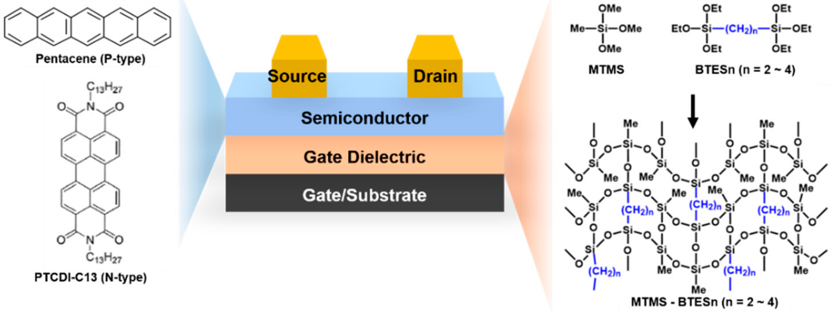
Figure 2.
AFM images (5 μm × 5 μm) of MTMS-BTESn copolymer gate dielectric films: (a) MTMS-BTES2, (b) MTMS-BTES3, and (c) MTMS-BTES4.
Figure 2.
AFM images (5 μm × 5 μm) of MTMS-BTESn copolymer gate dielectric films: (a) MTMS-BTES2, (b) MTMS-BTES3, and (c) MTMS-BTES4.

Figure 3.
Electrical properties of spin-coated copolymer films fabricated with various monomers (thickness: 100 nm): (a) Leakage current density vs electric field plot; (b) Capacitance-frequency plots (10–103 kHz); (c) Comparison of leakage current density and k value as a function of monomer type.
Figure 3.
Electrical properties of spin-coated copolymer films fabricated with various monomers (thickness: 100 nm): (a) Leakage current density vs electric field plot; (b) Capacitance-frequency plots (10–103 kHz); (c) Comparison of leakage current density and k value as a function of monomer type.

Figure 4.
Performance of OTFT devices on copolymer dielectric films. OTFT transfer characteristics for (a) P5, (c) PTCDI-C13, and OTFT output characteristics for (b) P5, (d) PTCDI-C13. The channel width and length are 1000 and 100 μm, respectively.
Figure 4.
Performance of OTFT devices on copolymer dielectric films. OTFT transfer characteristics for (a) P5, (c) PTCDI-C13, and OTFT output characteristics for (b) P5, (d) PTCDI-C13. The channel width and length are 1000 and 100 μm, respectively.


Figure 5.
OTFT devices fabricated on flexible PEN substrates. (a) Transfer characteristics using a PTCDI-C13 as semiconductor (channel width and length are 2000 and 50 μm, respectively); (b) Photo of flexible OTFT device.
Figure 5.
OTFT devices fabricated on flexible PEN substrates. (a) Transfer characteristics using a PTCDI-C13 as semiconductor (channel width and length are 2000 and 50 μm, respectively); (b) Photo of flexible OTFT device.


Table 1.
Properties of Copolymer Dielectrics based on MIS Device Structure (J, leakage current density; Ci, Capacitance; k, dielectric constants).
Table 1.
Properties of Copolymer Dielectrics based on MIS Device Structure (J, leakage current density; Ci, Capacitance; k, dielectric constants).
| Copolymer | Thickness (nm) | J (A·cm−2) at 1 MV·cm−1 | Ci (nF·cm−2) | k |
|---|---|---|---|---|
| MTMS-BTES2 | 140 | 8.11 × 10⁻⁸ | 23.0 | 3.60 |
| 100 | 1.24 × 10⁻⁸ | 30.8 | 3.47 | |
| 80 | 1.38 × 10⁻⁷ | 33.6 | 3.33 | |
| MTMS-BTES3 | 135 | 3.91 × 10⁻⁸ | 23.3 | 3.50 |
| 102 | 1.41 × 10⁻⁸ | 29.5 | 3.33 | |
| 90 | 1.20 × 10⁻⁸ | 32.2 | 3.27 | |
| MTMS-BTES4 | 150 | 5.27 × 10⁻⁸ | 20.5 | 3.47 |
| 113 | 6.55 × 10⁻⁸ | 29.1 | 3.31 | |
| 100 | 1.83 × 10⁻⁸ | 29.4 | 3.32 |
Table 2.
TFT Device Performance Parameters based on P5 and PTCDI-C13 Semiconductors on Copolymer Dielectric. (µsat: carrier mobility, Ion/Ioff: current on/off ratio, VT; threshold voltage).
Table 2.
TFT Device Performance Parameters based on P5 and PTCDI-C13 Semiconductors on Copolymer Dielectric. (µsat: carrier mobility, Ion/Ioff: current on/off ratio, VT; threshold voltage).
| Type | Semi-Conductor | µsat 1(cm2·V−1·s−1) | Ion/Ioff | VT (V) |
|---|---|---|---|---|
| p-type | P5 | 0.15 | 2.24 × 10⁵ | −10.5 |
| n-type | PTCDI-C13 | 0.09 | 3.00 × 10⁶ | 9.3 |
1 The average values obtained from six different devices.
© 2018 by the authors. Licensee MDPI, Basel, Switzerland. This article is an open access article distributed under the terms and conditions of the Creative Commons Attribution (CC BY) license (http://creativecommons.org/licenses/by/4.0/).
Share and Cite
MDPI and ACS Style
Kim, D.; Kim, C. A Ladder-Type Organosilicate Copolymer Gate Dielectric Materials for Organic Thin-Film Transistors. Coatings 2018, 8, 236. https://doi.org/10.3390/coatings8070236
AMA Style
Kim D, Kim C. A Ladder-Type Organosilicate Copolymer Gate Dielectric Materials for Organic Thin-Film Transistors. Coatings. 2018; 8(7):236. https://doi.org/10.3390/coatings8070236
Chicago/Turabian StyleKim, Dongkyu, and Choongik Kim. 2018. "A Ladder-Type Organosilicate Copolymer Gate Dielectric Materials for Organic Thin-Film Transistors" Coatings 8, no. 7: 236. https://doi.org/10.3390/coatings8070236
Note that from the first issue of 2016, this journal uses article numbers instead of page numbers. See further details here.