Significantly Reduced Secondary-Electron-Yield of Aluminum Sheet with Fluorocarbon Coating


1
State Key Laboratory of Power Transmission Equipment & System Security and New Technology, Chongqing University, Chongqing 400044, China
2
National Key Laboratory of Science and Technology on Space Microwave, China Academy of Space Technology (Xi’an), Xi’an 710100, China
*
Author to whom correspondence should be addressed.
Coatings 2018, 8(7), 249; https://doi.org/10.3390/coatings8070249
Submission received: 3 June 2018
/
Revised: 11 July 2018
/
Accepted: 13 July 2018
/
Published: 16 July 2018
Abstract
:In this work, the surface of Al sheet was coated with a fluorocarbon (FC) thin film by radio frequency (RF) sputtering of polytetrafluoroethylene (PTFE) to investigate the influence of dielectric coatings on the secondary electron yield (SEY) behavior of Al sheets. Atomic-force microscopy (AFM) and energy-dispersive spectroscopy (EDS) were employed to identify the surface topographies and elemental contents of the samples with FC coatings. Water contact angle (WCA) measurements were performed to characterize the surface tension as well as the polar and dispersion components of the samples’ surface. The secondary electron- mission (SEE) behavior of the samples was determined by measuring the SEY coefficients in an ultra-high vacuum chamber with three electron guns. The experimental results indicated that the longer sputtering time effectively led to the increase in coating thickness and a higher ratio of F/C, as well as the continued decrease of surface tension. A quite thin FC coating of about 11.3 nm on Al sheet resulted in the value of maximum SEY (δmax) dropping from 3.02 to 1.85. The further increase in coating thickness beneficially decreased δmax down to 1.60, however, at the cost of a ten-fold thicker coating (ca. 113 nm). It is found that increasing the coating thickness contributes to reducing SEY coefficients as well as suppressing SEE. The results are expected to guide the design of dielectric-coating for SEY reduction as well as multipactor suppression on Al.
1. Introduction
Secondary electron emission (SEE) is a phenomenon where primary incident electrons hitting a solid or passing through the surface layer of a solid, induce the emission of secondary electrons. It is a well-known phenomenon of electron-solid interactions that has been regarded as accounting for the multipactor effect in space-based systems. This detrimental effect is a self-sustained electron avalanche caused by the impingement of electrons against the metallic surface of microwave components accelerated by energy in an RF field. Multipactor discharge in space high-power microwave components may bring serious breakdown and insulation failure [1,2,3] which has inspired research on developing effective approaches to inhibit SEE [4,5,6]. Secondary electron yield (SEY) is frequently used as the index for describing SEE behavior and is defined as the proportion of secondary electron numbers to primary electron numbers. It is known that reducing SEY helps to suppress SEE.
Several studies have discovered two routes that leading to significantly reducing SEY: micro-structured surfaces and surface coating with passivation layers [7,8]. The geometrical morphology of a sample surface can be tailored to create triangular, rectangular and micro-porous grooves through several approaches such as laser lithography and laser and chemical etching. Parts of the primary incident electrons are trapped in the grooved structures by changing its trajectory, thus restraining SEE [9,10,11,12]. On the premise of a large depth-to-width ratio and high aspect ratio, rough surfaces with irregular structures created by artificial means also work. The surface roughness is likely to act as a blackbody or rough surface cage. Particle bombardment is an emerging and promising method to prepare rough surfaces with reduced SEY. Yang et al. [13] found that argon ion sputtering reduced the SEY of gold by eliminating contamination but also the roughing surface induced ion bombardment. An “equivalent work-function” relating the effect of contamination and surface roughness was proposed to predict SEY. Furthermore, Hu et al. [14] analyzed the influence of bombardment intensity and ion energy on the SEY of copper plates. Based on different surface topographies fabricated by ion bombardment, the optimized ion-beam parameters to achieve the lowest SEY of copper were obtained. In association with the experimental construction of rough structures, numerical simulation and dynamic calculation have developed rapidly. Theoretical research has mainly focused on building up rough-structure models, which consider the energy and incident angle of primary electrons. Chang et al. [15] applied particle-in-cell simulation to analyze the changes of SEY and the multipactor threshold when surfaces vary from flat to grooved shapes. It was concluded that periodic grooved structures effectively reduced SEY and raised surface flashover voltage in high RF fields. A numerical multi-generation model from Cao et al. has contributed to in-depth understanding of the SEE behavior of rough metal surfaces [16]. Although the micro-structured surface has proved effective in reducing SEY, it is lacks optimized structure parameters and the characterization of their impact on the performance of microwave components.
Coating passivation films with relatively low SEY on samples was found to be another effective approach to reduce the SEY of metals. Due to the intrinsically low SEY of carbon coatings, aquadag, vacuum pyrolized glyptal and lamp black deposited by electrophorese were analyzed to increase the power throughput to a plasma of an existing lower hybrid waveguide [17]. Gold and silver with their good physical and chemical properties, are traditional metallic passivation films [18,19]. The chemical stability against ambient conditions and good electrical conductivity of these coatings make them beneficial for storage, transportation and installation of devices. However, the high cost of noble metals limits their applications. Thus, a growing number of novel coatings have been considered. Titanium nitride, chromium nitride and carbon nitride are typical candidates [20]. The effect of thickness, elemental content and geometric morphology of the novel coatings on reducing SEY have been investigated [21,22]. Based on the measured SEY, numerical simulation is employed to calculate multipactor threshold and to ensure the effectiveness and feasibility of proposed treatment approaches for microwave power components [23,24]. However, during storage and operation, the above inorganic passivation films were not stable enough to counter mechanical vibrations and temperature shocks. These factors may lead to micro-cracks which result in coating flake off and increasing SEY values.
Fluorocarbon (FC) film with its excellent properties, including high resistivity, chemical inertness and lower Young’s modulus, has been found to be a promising passivation coating for application in the mechanical, electrical and medical industries. The FC film is mainly amorphous and is typically prepared by the sol-gel method [25], chemical vapor deposition (CVD) [26] and physical vapor deposition (PVD). Some pioneers have explored several preparation methods for FC film by PVD, such as vacuum evaporation and magnetron sputtering. The optical, physical and chemical properties of FC films have been discussed in few articles [27,28,29]. More research is needed on the application of FC films to reduce SEY and examine the dynamics during the deposition of FC films.
This work intends to coat Al sheets with FC films by sputtering technology, which is expected to obtain FC films with different thickness to reduce the SEY values of Al. The surface geometrical morphology, elemental contents, and surface tension characteristics of the samples are assessed using various approaches such as AFM, EDS and WCA measurements.
2. Materials and Methods
An aluminum roll with purity of better than 99.99% was cut into 1 mm × 6 mm (thickness × diameter) circular sheets. The sheets were subsequently cleaned by sonication for 20 min with acetone, anhydrous alcohol and de-ionized water, successively. With the RF magnetron sputtering, a PTFE disk with thickness of 4 mm was used as the target. The FC film was deposited on the Al sheet by sputtering in argon at 0.5 Pa. The voltage and current during sputtering were controlled as 500 V and 160 mA, respectively. The distance between the Al sheet and the PTFE target was set as 100 mm. The thickness of the FC coating was controlled by the sputtering duration which was 10, 20, 60 and 100 min, and the thickness values were metered by a surface profiler (Dektak XT, Bruker, Germany).
The polar component and dispersion component of surface tension were determined by the Owens-Wendt-Kaelble (OWK) approach and the Young’s equation (Equations (1) and (2)) [30]. The OWK approach includes dispersion component, hydrogen bonding and dipole-dipole interactions of the surface tension. This approach is an extension of the Fowkes’ concept [31].
The parameters of θ and γL in Equation (2) stand for the measured contact angles and the known surface tension of liquids. Diiodomethane and water were considered as nonpolar and polar droplets (each 20 μL), respectively, to evaluate the surface tension of samples. An AFM (XE-7, Parker, Korea) working at non-contact mode was utilized to obtain the value of mean square deviation Ra of the samples’ surface roughness. The field emission scanning electron microscope with X-ray energy dispersive spectroscopy (FESEM/EDS, Tokyo, Japan) with a beam accelerating voltage of 8 kV was used to determine elemental compositions of specimens. The FESEM (JSM-7800F, JEOL, Tokyo, Japan) provided topographical information of the sample surface. X-rays with sufficient energy escaping sample surfaces were detected to produce a spectrum with peaks at the characteristic energies of the elements present. The spectrum provided semi-quantitative elemental composition information of the sample surface.
The SEY behavior of samples was measured in an ultra-high vacuum chamber with base pressure of 2 × 10⁻⁶ Pa. The chamber was equipped with a measuring electron gun and two neutralization electron guns (G1 and G2). Both guns were controlled by voltage pulses to be maintained as low and high energy levels, respectively. The two guns are applied to neutralize the charging state (from either positive or negative to zero) of samples during each measurement interval (Figure 1). The cathode of G1 and the sample holder were grounded so as to neutralize positive charges of the measured sample during each measurement interval. This arrangement meant that the electrons from G1 could not reach the sample if its surface was accumulated with negative charges. The energy of electrons emitted from G2 was set higher than the first cross-over energy E1 (the lowest primary energy at which SEY = 1), which led the surface potential of the sample to be increased by the electrons from G2. For the interval between measurements, the working time of G1 was set to be sufficiently long to guarantee that the surface potential of the sample was neutralized before the next measurement. In order to remove possible contamination and absorbed air molecules on the sample surface, all samples were treated by ion cleaning at the energy of 500 eV for about 20 min before the SEY measurements. The measuring electron gun generated primary electrons with energy varying from 0 to 4000 eV. The incident beam current Ip for the SEY measurement was considered as the current ejecting to the sample holder (i.e., without sample installed) by the measuring gun. The SEY current Is was collected by the collecting electrode and was measured via an electrometer (Keithley 6517B, Keithley Instruments, Cleveland, OH, USA). Therefore, δ was determined as δ = Is/Ip. More information is available in [32].
3. Results and Discussion
3.1. Characterization of Fluorocarbon (FC) Coatings
Table 1 summarizes the surface characteristics of FC coatings with different thickness. It is seen that the increased thickness of FC coatings leads to the increasing of WCA. An 11.3 nm coating resulted in the WCA increasing from 101.6° to 110.5°. However, an increase in the WCA from 110.5° to 120.9° is achieved at the cost of FC coating that is ten-fold thicker, i.e., from 11.3 to 113 nm. The FC coating, as well as showing an increase in thickness, leads the dispersion component , steeply increasing from 5.6 to 330.3 N/m then dropping to 7.8 N/m. Meanwhile, the polar component shows a decrease from 37.3765 mN/m for Al sheets to 13.3788 mN/m for the Al sheet with 113 nm FC coating.
The exists in every substance because it signals the Van-der-Waals interaction between all atoms and molecules. The of surface tension is caused by the interactions between two induced dipoles while the results from the potential energy of Coulomb interactions between two permanent dipoles. As is well-known, an Al sheet is protected by a thin layer of Al2O3. This Al2O3 layer is dominated by the dipole-dipole interaction and subordinated induced-dipole interaction, which should lead to the result that is much higher than [33]. With the FC coating, is decreased and changes oppositely, which indicates that the electron induction effects from the electronegative fluorine is much more obvious. This is because the F atoms are electron donor sites and electron acceptor sites appear on the Al atoms, which leads to increased amounts of induced-dipoles and the resultant increased dispersion component [34].
The lower surface tension of fluorine elements in FC coating is beneficial for the significant increase in WCA. The increase in the thickness of the FC layer leads to the decrease of both and . Although the fluorine content increases (Figure 2) in thicker FC layers, the should not be strongly dependent the increased thickness of the FC layer. This is due to the fact that the interaction between F and Al atoms tends to disappear in thicker FC layers. Therefore, the prominent enhancement of surface roughness (Figure 3) should play the key role in decreasing the . On the other hand, keeps decreasing which is caused by the introduction of fluorine elements that exhibit quite low surface tension. The ionic polar Al2O3 layer endows the and determines the surface tension for the Al substrate sheet, which is manifested by the ratio of / = 6674. The very thin layer of FC coating (e.g., 11.3 nm) is sufficient to drop this ratio to 54. However, further increase of the FC coating thickness results in the increase of / for example, / = 1715 corresponding to the 113 nm FC layer. The increase of / is probably caused by the imperfect stacking of the FC layer which can be evidenced by the AFM results (Figure 3) [35].
The chemical compositions of FC coatings show significant dependence on the layer thickness, i.e., sputtering duration. Figure 2 provides a semi-quantitative view of the elemental compositions in weight percent. The oxygen is traceable by the observed small value of 2 wt %, which confirms the existence of the very thin oxide layer (OL) on the Al surface. The beam accelerating voltage of 8 kV results in X-ray generation depth that is well over a micron, which is far more than the total thickness of the FC coating and OL. This makes it reasonable that minor amounts of oxygen remain regardless of the thickness of FC layer. With the FC coating and its increased thickness ion Al sheets, F and C elements appear and show significant variation upon different FC layer thickness. It should be noted that the weight percentages of F and C increase sharply with the increasing layer thickness. The ratio F/C increases from 10.69% to 63.94% upon the thickness increasing from 11.3 to 113 nm. A lower F/C indicates large amounts of unsaturated components (UCs), typically, C–F and C–C. Longer duration of sputtering enhances saturated components (SCs) such as CF2 and CF3.
The increase in the F/C ratio with increased thickness arises from the developing dissociation-synthesis-growth process by momentum transfer and polymerization during deposition [36]. This process involves energetic atomic-sized Argon ions as well the F and C atoms in the PTFE target. During sputtering, momentum transfers from the bombarding Argon ions to the F and C atoms of the target, which results in their ejection. The ejected atoms diffuse towards the Al sheet and are deposited. This process is influenced by the fact that the atomic mass of C is lighter than that of F, which leads to C being easier to ballistically fly from the PTFE target in straight lines and impact energetically on the Al substrate. The deposited C afterwards acts as a nucleus which contributes to the improved deposition of F. As observed, the increased F/C in thicker films is the result of the increased carbon-fluorine coordination in the FC film. For long-time sputtering (corresponding to thicker FC films CF, CF2 and CF3 which are the most dominant radials are noticeable, as are CF4, C2F4, C2F6 and C3F8, which are the most important stable gases during sputtering [37]. These components serve as precursors to the plasma polymerization process which results in deposition of the FC film [38,39].
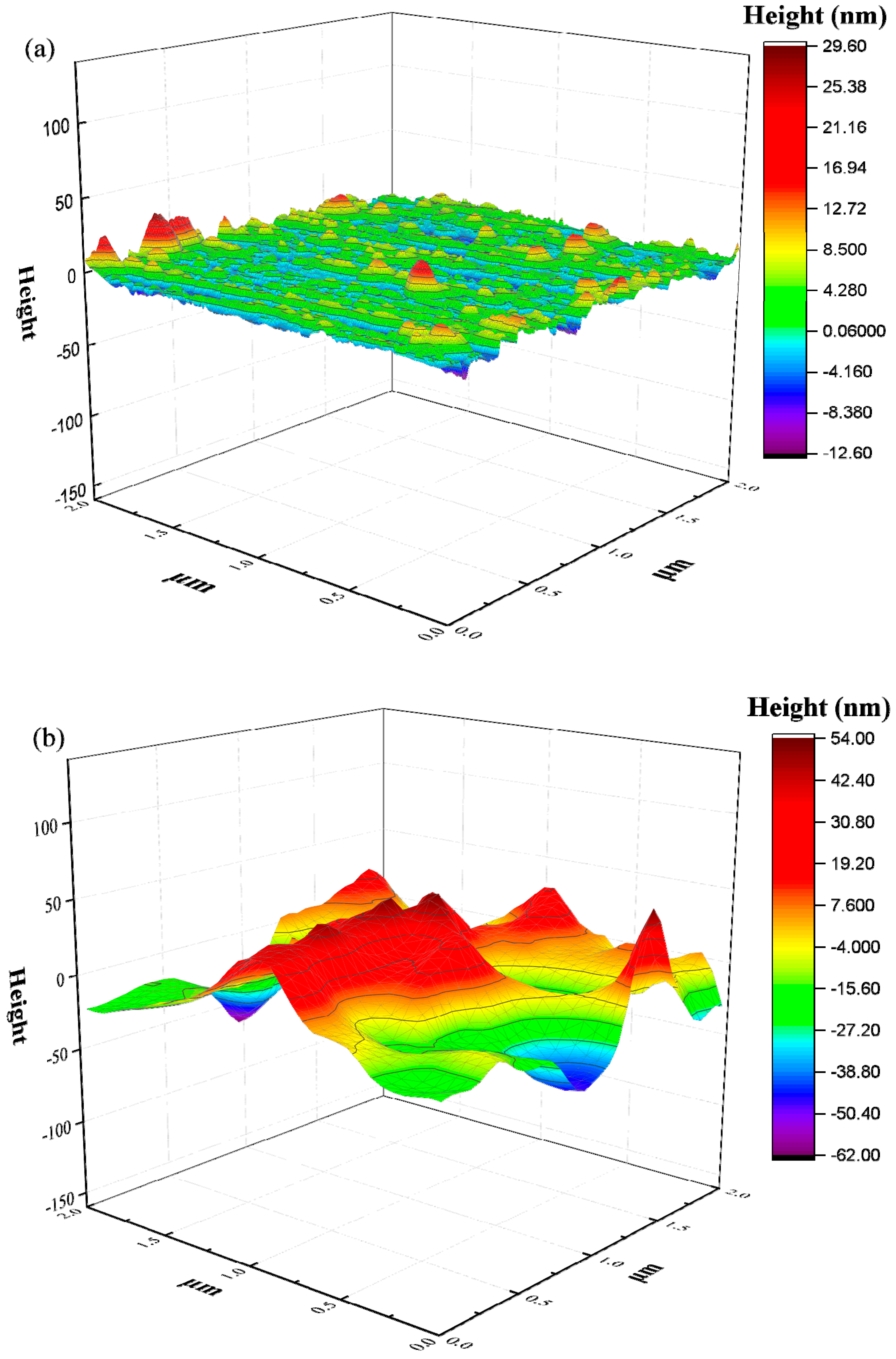
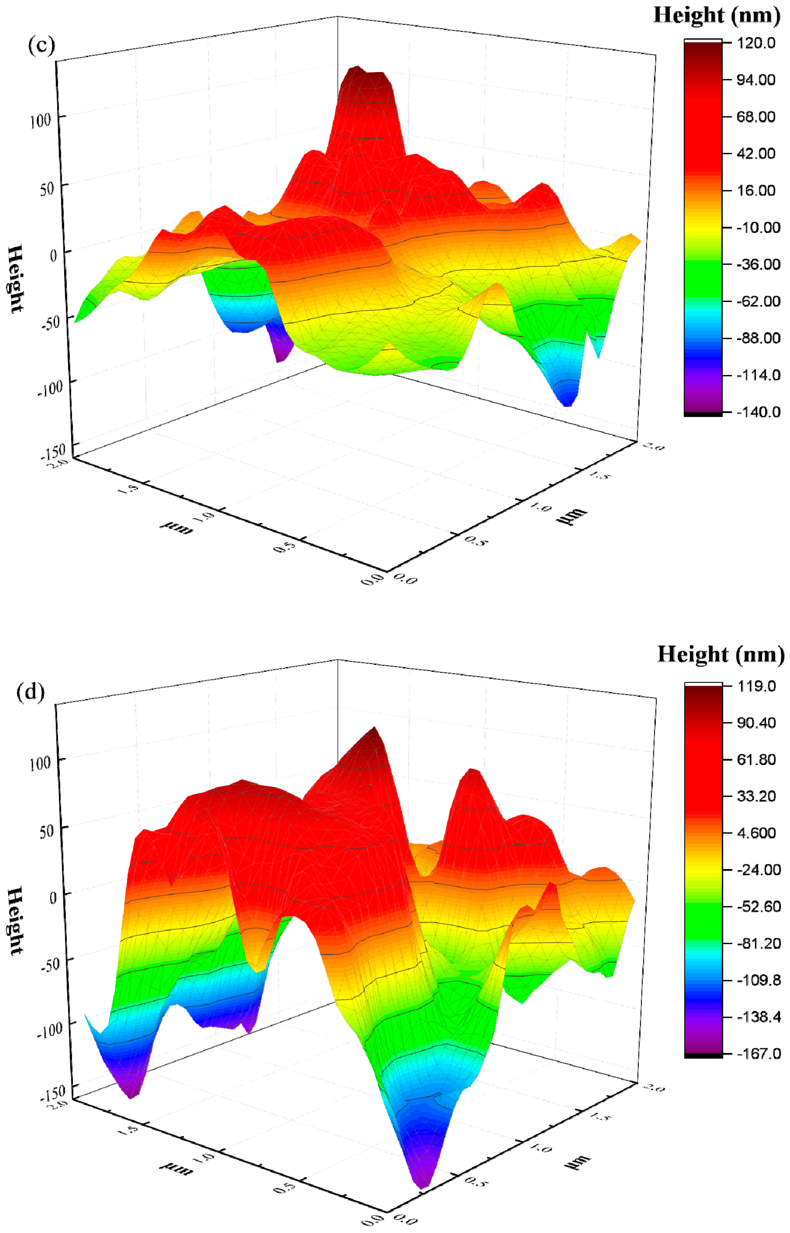
The surface morphology of samples measured by AFM are shown in Figure 3. With the FC coating and its increasing thickness, all samples exhibit an increase in surface roughness. The Al sheet without FC coating has a quite smooth surface with Ra~3.3 nm and the value of valley-to-peak Rpv is around 50 nm (Figure 3a). The 11.3 nm FC layer has changed the Ra from 3.3 to 11.8 nm and the Rpv reaches 116 nm (Figure 3b). The further increasing of layer thickness from 67.8 nm to 113 nm results in the increment of Ra from 35.2 nm to 48.6 nm. Meanwhile, the corresponding Rpv rises from 260 nm to 286 nm (Figure 3c,d).
During sputtering, the coating process of the FC layer is usually considered as an assembly of multiple levels of layers. It starts from the initial activated nucleus which introduces serried grain forming on the surface of Al sheet. This is followed by the merging of the serried grains and the subsequent forming of a semi-continuous three-dimensional network layer. The formation of the semi-continuous layer achieves coverage of 50%–70%. This provides the conditions for the serried grains of the next layer to begin to grow.
There are at least three factors which could be involved on determining the surface roughness: the planted grains, the network structure of the semi-continuous layer, and the surface roughness of the Al sheet [40]. During sputtering and the layer stacking, the planted grains growing on Al sheet tend to curl due to the surface roughness of the Al sheet followed by further growing as well merging of grains. The surface roughness is expected to reach a saturation value, which is proved by the AFM measurements (Figure 3). This is due to the process whereby the semi-continuous layer is gradually filled by grain merging, which results in less porosity of the mesh structure.
3.2. Secondary Electron Yield (SEY) Analysis
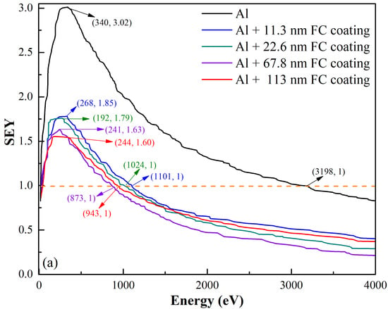
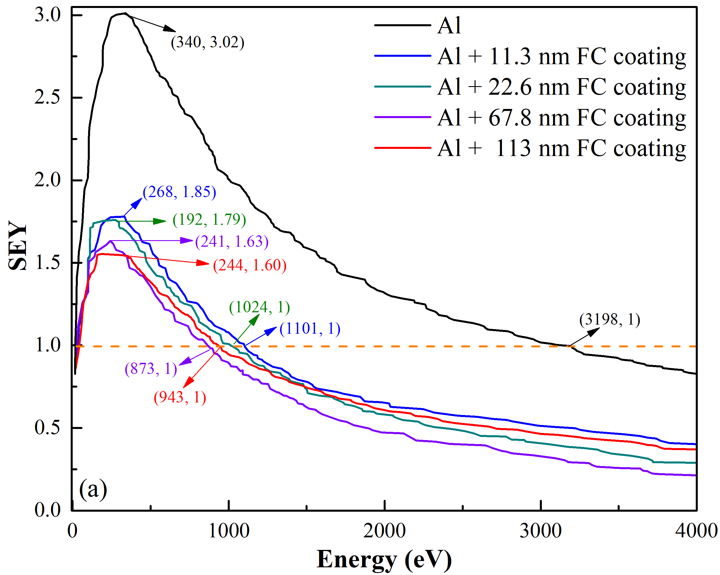
Figure 4a shows the SEY coefficient δ of Al sheet and the sheet coated by an FC layer with different thicknesses as a function of primary electron energy, which varies between 0 and 4000 eV. Figure 4b is enlarged for a better view of the zone for energy lowers than 60 eV. Depending on the energy of the primary electrons, they will be able to penetrate up to a certain depth R in the sample. The value of R is small for the very low energy primary electrons. This leads to the fact that the secondary electrons easily escape and the δ rises with the growth of primary electrons energy. For primary electrons with very high energy, the quite large R means most secondary electrons are generated at a greater depth, which suppresses their escape due to the significantly prolonged escape path and increased energy dissipation. This leads to the fact that SEY decreases with the increasing energy of the primary electrons. Hence, the SEY coefficient δ has a maximum value δmax at a certain energy of the primary electrons. The results in Figure 4 show the δmax of the Al sheet decreases from 1.85 to 1.60 via 1.79, 1.63 with the thickness of FC coatings increasing from 11.3 to 113 nm via 22.6 and 67.8 nm. The corresponding primary electron energy Emax is 268, 192, 241, and 244 eV, respectively. When the δmax value of the Al sheet is 3.02, a sharp drop appears with 11.3 nm FC coating on the Al sheet. Further increases of the FC coating thickness may result in an even lower δmax value of 1.60, however this is at the cost of a ten-fold increase in the thickness of 113 nm.
The first-increase, later-decrease behavior of the SEY coefficient (δ) gives two crossover points E1 and E2 at which δ = 1. The primary electrons with an energy level between E1 and E2 can introduce more than one secondary electron on average, which initiates the occurrence of multipactor discharge and the resulting surface breakdown. Primary electrons with energy below E1 or above E2 should excite less of secondary electrons, and multipactor discharge will be suppressed. The E1 of Al sheet is 18 eV and this value increases from 28 to 43 eV as the result of increasing the FC coating thickness from 11.3 to 113 nm. This confirms that thicker FC coating helps to enhance E1 which may lead to an increase in the multipactor threshold. The E2 of Al sheet has a quite high primary electron energy of 3180 eV. A very thin FC coating of 11.3 nm on Al sheet is sufficient to reduce the E2 down to 1073 eV. Further increases in the thickness of the FC coating seem to only generate fluctuation of E2. The FC coating with thicknesses from 22.6 to 113 nm gives rise to E2 first decreasing from 993 to 873 eV, then increasing to 900 eV. It is apparent that a thin layer of FC coating is quite close to the optimal thickness value in order to significantly suppress the SEE for Al sheets.
The maximum values (δmax) for Al sheets coated by FC layers are summarized in Figure 5 for better comparison. It is well-known that fluorocarbon polymers have good capability for negative-charge storage [41]. Our results showed that the 11.3 nm FC thin film holds a surface potential value of around 20 V after negative corona charging. Because of the FC layer’s capacity to store charge, it should capture some of the primary electrons. This surface potential value corresponds to a quite high electron density of around 10 mC/m2. Therefore, the captured electrons are able to decrease SEY by reducing the ejection energy and number of primary electrons, which accounts for the right shifting of E1 with increasing FC-layer thickness.
FC coating is composed of C–F and C–C bonds (Figure 2). The bond length of Al–Al is about 280 pm, while the values for C–C and C–F are about 135 and 154 pm, respectively. The much-narrower lengths of C–C and C–F should enhance the difficulty, i.e., energy loss, for primary electrons to penetrate through the FC layer as well as for secondary electrons to leave the sample surface [42]. They both play a role in reducing the number of secondary electrons, which leads to the sharp decrease of δmax from 3.02 to 1.85 when the Al sheet is coated by a 11.3 nm thick FC layer.
When primary electrons impinge upon the sample surface, some of the primary electrons are back scattered elastically while other electrons penetrate and interact with the sample to produce true-secondary electrons, which contribute to SEY. We have A ~ A0 (Φ/Φ0)−3 which is an empirical correlation to express the behavior that the increasing equivalent work-function Φ should reduce the escape probability A of the true-secondary electrons [43], which A0 and Φ0 as the two constants for adapting the experimental results. Some results have proved that an increase of Φ usually relates to reduction of surface tension [44,45,46,47]. It is seen from Table 1 that the surface tension of samples reduces as a result of the FC layer thickness increasing. This agrees with the observed phenomena that lower surface tension is beneficial to reduce the escape probability A, which accounts for the reduced SEY coefficient. In addition, the increasing of Ra is beneficial for secondary electrons to collide and be absorbed by the side walls of the micro-structured surface. Less surface area is applied to electron emission for higher Ra, so SEY coefficient is reduced by increasing surface roughness.
The experimental δmax of Al sheet is affected by the purity and surface roughness of Al, as well as the air exposure condition. The measured δmax for Al may vary from case to case. As there is an oxide-layer on the surface of Al sheet, the δmax of the measured sample corresponds to the value of A2O3 in Seiler’s study. When Al sheets are coated by FC, the δmax of the FC coated Al sheet is in the range of δmax for insulators [48]. Montero has found that the Al sheet with purity of 99.999% exhibits a δmax of 3.2 while the value for Al sheet with purity of 99% is smaller at 2.7 [49]. We found the Al with purity of 99.99% had an δmax = 3.02, which agrees well with the range determined by Montero.
4. Conclusions
In this work, the results of measuring the SEY of Al sheets with various FC coating thickness are presented. A significant reduction in SEY is possible when 113 nm FC coating was deposited on the surface of Al sheet. An increase in coating thickness is also found to narrow the gap between E1 and E2, i.e., the E1 increased from 18 to 43 eV and the E2 decreased from 3198 to 873 eV. The charge storage capacity and surface roughness of the FC coating appears to be the main causes of SEE suppression. The Al sheet with thicker coating, which exhibited a higher F/C ratio and lower surface tension is expected to have better effect on SEY reduction and multipactor suppression.
Author Contributions
Formal Analysis, F.W.; Investigation, Q.Z.; Resources, J.L. and K.W.; Data Curation, Z.H. and W.C.; Writing-Original Draft Preparation, F.W. and Q.Z.; Writing-Review & Editing, F.W. and Q.Z.
Funding
This research was funded by the National Natural Science Foundation of China (U1537211), National Key Basic Research Program of China (973 Program) (2015CB251003), National Natural Science Foundation of China (51507017), and National “111” Project of the Ministry of Education of China (B08036).
Acknowledgments
We acknowledge Kangcheng Qi from the University of Electronic Science and Technology of China for his assistance in SEY measurements.
Conflicts of Interest
The authors declare no conflict of interest.
References
- Rasch, J.; Anderson, D.; Semenov, V.E. Multipactor breakdown in microwave pulses. J. Phys. D Appl. Phys. 2013, 46, 505201. [Google Scholar] [CrossRef] [Green Version]
- González-Iglesias, D.; Pérez, A.M.; Monerris, O. Recent advances of the multipactor RF breakdown in RF satellite microwave passive devices. In Proceedings of the Progress in Electromagnetic Research Symposium (PIERS), Shanghai, China, 8–11 August 2016; pp. 4401–4405. [Google Scholar]
- Woode, A.; Petit, J. Investigations into multipactor breakdown in satellite microwave payloads. ESA J. 1990, 14, 467–478. [Google Scholar]
- Sattler, J.M.; Coutu, R.A.; Lake, R.; Laurvick, T.; Back, T.; Fairchild, S. Modeling micro-porous surfaces for secondary electron emission control to suppress multipactor. J. Appl. Phys. 2017, 122, 055304. [Google Scholar] [CrossRef]
- He, Y.N.; Peng, W.B.; Cui, W.Z.; Ye, M.; Zhao, X.L.; Wang, D.; Hu, T.C.; Wang, R.; Li, Y. Thermal evaporated hyperbranched Ag nanostructure as an effective secondary-electron trapping surface coating. AIP Adv. 2016, 6, 025122. [Google Scholar] [Green Version]
- Zhang, N.; Wang, R.; Li, Y.; Cui, W.Z. Simulation of metal surfaces secondary electron emission in multipactor. In Proceedings of the 2011 International Conference on Electronics, Communications and Control (ICECC), Ningbo, China, 9–11 September 2011; pp. 4520–4522. [Google Scholar] [CrossRef]
- Suetsugu, Y.; Fukuma, H.; Shibata, K.; Tsukuba, J.M.; Pivi, L.; Wang, S. Experimental studies on grooved surfaces to suppress secondary electron emission. In Proceedings of the 1st International Particle Accelerator Conference (IPAC’10), Kyoto, Japan, 23–28 May 2010; pp. 2021–2023. [Google Scholar]
- Fuentes, G.G.; Rodríguez, R.J.; García, M.; Galán, L.; Montero, I.; Segovia, J.L.D. Spectroscopic investigations of Cr, CrN and TiCr anti-multipactor coatings grown by cathodic-arc reactive evaporation. Appl. Surf. Sci. 2007, 253, 7627–7631. [Google Scholar] [CrossRef]
- Pivi, M.; King, F.K.; Kirby, R.E.; Raubenheimer, T.O.; Stupakov, G.; Le Pimpec, F. Sharp reduction of the secondary electron emission yield from grooved surfaces. J. Appl. Phys. 2008, 104, 104904. [Google Scholar] [CrossRef] [Green Version]
- Ye, M.; He, Y.N.; Hu, S.G.; Wang, R.; Hu, T.C.; Yang, J.; Cui, W.Z. Suppression of secondary electron yield by micro-porous array structure. J. Appl. Phys. 2013, 113, 074904. [Google Scholar] [CrossRef]
- Ye, M.; He, Y.N.; Hu, S.G.; Yang, J.; Wang, R.; Hu, T.C.; Peng, W.B.; Cui, W.Z. Investigation into anomalous total secondary electron yield for micro-porous Ag surface under oblique incidence conditions. J. Appl. Phys. 2013, 114, 104905. [Google Scholar]
- Cui, W.; Wang, R.; Hu, T.; Yang, J.; He, Y.N. Improvement multipactor discharge of microwave components by micro-porous surface. In Proceedings of the 16th International Symposium on Antenna Technology and Applied Electromagnetics (ANTEM), Victoria, BC, Canada, 13–16 July 2014; pp. 1–2. [Google Scholar] [CrossRef]
- Yang, J.; Cui, W.Z.; Li, Y.; Xie, G.B.; Zhang, N.; Wang, R. Investigation of argon ion sputtering on the secondary electron emission from gold samples. Appl. Surf. Sci. 2016, 382, 88–92. [Google Scholar] [CrossRef]
- Hu, X.-C.; Cao, M.; Cui, W.-Z. Influence of surface topography on the secondary electron yield of clean copper samples. Micron 2016, 90, 71–77. [Google Scholar] [CrossRef] [PubMed]
- Chang, C.; Huang, H.J.; Liu, G.Z.; Chen, C.H.; Hou, Q.; Fang, J.Y. The effect of grooved surface on dielectric multipactor. J. Appl. Phys. 2009, 105, 391–392. [Google Scholar] [CrossRef]
- Cao, M.; Zhang, N.; Hu, T.-C.; Wang, F.; Cui, W.-Z. Secondary electron emission from rough metal surfaces: A multi-generation model. J. Phys. D Appl. Phys. 2015, 48, 055501. [Google Scholar] [CrossRef]
- Ruzic, D.; Moore, R.; Manos, D.; Cohen, S. Secondary electron yields of carbon-coated and polished stainless steel. J. Vac. Sci. Technol. 1982, 20, 1313–1316. [Google Scholar] [CrossRef] [Green Version]
- Nistor, V.; González, L.A.; Aguilera, L.; Montero, I.; Galán, L.; Wochner, U. Multipactor suppression by micro-structured gold/silver coatings for space applications. Appl. Surf. Sci. 2014, 315, 445–453. [Google Scholar] [CrossRef]
- Li, J.; Hu, W.; Wei, Q.; Wu, S.; Hua, X.; Zhang, J. Electron-Induced Secondary Electron Emission Properties of MgO/Au Composite Thin Film Prepared by Magnetron Sputtering. J. Electron. Mater. 2017, 46, 1466–1475. [Google Scholar] [CrossRef]
- Diaz, N.; Casraneda, S.; Ripalda, J.M.; Montero, I.; Galan, L.; Feltham, S.; Rabosa, D.; Rueda, F. Materials of Low Secondary Electron Emission to Prevent the Multipactor Effect in High-Power RF Devices. In Proceedings of the 6th Spacecraft Charging Conference, Hanscom AFB, MA, USA, 2–6 November 1998; pp. 205–209. [Google Scholar]
- Zhang, N.; Kang, Y.; Wang, R.; Cui, W.Z. A new surface treatment for suppressing multipactor in microwave components. In Proceedings of the 2012 International Conference on Microwave and Millimeter Wave Technology (ICMMT), Shenzhen, China, 5–8 May 2012; pp. 1–3. [Google Scholar]
- Wang, J.; Wang, Y.; Xu, Y.H.; Zhang, X.Y.; Zhang, B.; Wei, W. Secondary electron emission characteristics of graphene films with copper substrate. Chin. Phys. C 2016, 40, 180–183. [Google Scholar] [CrossRef]
- Li, Y.; Cui, W.-Z.; Wang, H.-G. Simulation investigation of multipactor in metal components for space application with an improved secondary emission model. Phys. Plasmas 2015, 22, 053108. [Google Scholar] [CrossRef]
- Nagesh, S.K.; Revannasiddiah, D.; Shastry, S.V.K. Investigation of multipactor breakdown in communication satellite microwave co-axial systems. Pramana 2005, 64, 95–110. [Google Scholar] [CrossRef]
- Piccinini, F.; Levi, M.; Turri, S. Photoactive sol–gel hybrid coatings from modified fluorocarbon polymers and amorphous titania. Prog. Org. Coat. 2013, 76, 1265–1272. [Google Scholar] [CrossRef]
- Yasuoka, H.; Yoshida, M.; Sugita, K.; Ohdaira, K.; Murata, H.; Matsumura, H. Fabrication of PTFE thin films by dual catalytic chemical vapor deposition method. Thin Solid Films 2008, 516, 687–690. [Google Scholar] [CrossRef]
- Stelmashuk, V.; Biederman, H.; Slavínská, D.; Zemek, J.; Trchová, M. Plasma polymer films RF sputtered from PTFE under various argon pressures. Vacuum 2005, 77, 131–137. [Google Scholar] [CrossRef]
- Jafari, R.; Menini, R.; Farzaneh, M. Superhydrophobic and icephobic surfaces prepared by RF-sputtered polytetrafluoroethylene coatings. Appl. Surf. Sci. 2010, 257, 1540–1543. [Google Scholar] [CrossRef] [Green Version]
- Nagayama, Y.; Iwamori, S.; Yamada, Y. Mechanical properties of polytetrafluoroethylene (PTFE) thin film sputtered on the metal substrates. Shinku 2003, 46, 827–834. [Google Scholar] [CrossRef]
- Martinelli, E.; Sarvothaman, M.K.; Alderighi, M.; Galli, G.; Mielczarski, E.; Mielczarski, J.A. PDMS network blends of amphiphilic acrylic copolymers with poly(ethylene glycol)-fluoroalkyl side chains for fouling-release coatings. I. Chemistry and stability of the film surface. J. Polym. Sci. Part A Polym. Chem. 2012, 50, 2677–2686. [Google Scholar] [CrossRef]
- Fowkes, F.M. Additivity of Intermolecular Forces at Interfaces. I. Determination of the contribution to surface and interfacial tensions of dispersion forces in various liquids. J. Phys. Chem. 1963, 67, 2538–2541. [Google Scholar] [CrossRef]
- Qun, W. Research on the Measurement Device of Secondary Electron Emission Coefficient. Master’s Thesis, University of Electronic Science and Technology of China, Chengdu, China, 2016. (In Chinese). [Google Scholar]
- Holysz, L.; Chibowski, E. Surface free energy components of alpha-alumina from thin-layer wicking. Langmuir 1992, 8, 717–721. [Google Scholar] [CrossRef]
- Desiraju, G.R.; Ho, P.S.; Kloo, L.; Legon, A.C.; Marquardt, R.; Metrangolo, P.; Politzer, P.; Resnati, G.; Rissanen, K. Definition of the halogen bond (IUPAC recommendations 2013). Pure Appl. Chem. 2013, 85, 1711–1713. [Google Scholar] [CrossRef]
- Qi, H.; Zhang, Y.; Di, J.; Du, W. Morphology and structure of polymer fluorocarbon coatings on polyimide by sputtering. Surf. Coat. Technol. 2007, 201, 5522–5525. [Google Scholar] [CrossRef]
- Alfonso, E.; Olaya, J.; Cubillos, G. Thin Film Growth through Sputtering Technique and Its Applications. In Crystallization Science and Technology; Andreeta, M., Ed.; IntechOpen Limited: London, UK, 2012; pp. 397–432. [Google Scholar] [CrossRef]
- Biederman, H. Organic films prepared by polymer sputtering. J. Vac. Sci. Technol. A 2000, 18, 1642–1648. [Google Scholar] [CrossRef]
- Mathias, E.; Miller, G. The decomposition of polytetrafluoroethylene in a glow discharge. J. Phys. Chem. 1967, 71, 2671–2675. [Google Scholar] [CrossRef]
- Biederman, H.; Stelmashuk, V.; Kholodkov, I.; Choukourov, A.; Slavı́Nská, D. RF sputtering of hydrocarbon polymers and their derivatives. Surf. Coat. Technol. 2003, 174–175, 7–32. [Google Scholar] [CrossRef]
- Shao, J.J.; Ren, Z.; Yang, Y.; Xiao, Y.; Yuan, Y.; Huang, J. Low temperature super-hydrophobicity of magnetron sputtered polytetrafluoroethylene coatings. Chin. J. Vac. Sci. Technol. 2017, 37, 154–160. (In Chinese) [Google Scholar]
- Sessler, G.M. Electrets; Springer: Berlin, Germany, 1987. [Google Scholar]
- Cao, M.; Zhang, X.S.; Liu, W.H.; Wang, H.G.; Li, Y.D. Secondary electron emission of graphene-coated copper. Diam. Relat. Mater. 2017, 73, 199–203. [Google Scholar] [CrossRef]
- Cazaux, J. Calculated influence of work function on SE escape probability and secondary electron emission yield. Appl. Surf. Sci. 2012, 257, 1002–1009. [Google Scholar] [CrossRef]
- Babich, A.V.; Pogosov, V.V. Electron work function and the surface tension of a metallic surface with an insulating coating. Phys. Met. Metallogr. 2008, 106, 332–340. [Google Scholar] [CrossRef]
- Abraham, F.; Ford, W.E.; Scholz, F.; Nelles, G.; Sandford, G.; von Wrochem, F. Surface Energy and Work Function Control of AlOx/Al Surfaces by Fluorinated Benzylphosphonic Acids. ACS Appl. Mater. Interfaces 2016, 8, 11857–11867. [Google Scholar] [CrossRef] [PubMed] [Green Version]
- De Waele, S.; Lejaeghere, K.; Sluydts, M.; Cottenier, S. Error estimates for density-functional theory predictions of surface energy and work function. Phys. Rev. B 2016, 94, 235418. [Google Scholar] [CrossRef]
- Cheng, S.; Tan, C.M.; Deng, T.; He, F.; Zhang, S.; Su, H. Investigation of work function and surface energy of aluminum: An ab-initio study. In Proceedings of the 2013 IEEE 5th International Nanoelectronics Conference (INEC), Sentosa, Singapore, 2–4 January 2013; pp. 473–475. [Google Scholar] [CrossRef]
- Heiler, H. Secondary electron emission in the scanning electron microscope. J. Appl. Phys. 1983, 54, R1–R18. [Google Scholar] [CrossRef]
- Montero, I.; Aguilera, L.; Dávila, M.E.; Nistor, V.C.; González, L.A.; Galán, L. Secondary electron emission under electron bombardment from graphene nanoplatelets. Appl. Surf. Sci. 2014, 291, 74–77. [Google Scholar] [CrossRef] [Green Version]
Figure 1.
Schematic diagram of secondary electron yield measurement.

Figure 2.
Chemical compositions and F/C ratio of measured samples with difference layer thickness. The lines are for guiding the eyes.
Figure 2.
Chemical compositions and F/C ratio of measured samples with difference layer thickness. The lines are for guiding the eyes.

Figure 3.
Surface morphology detected by Atomic-force microscopy (AFM) for fluorocarbon (FC) coating with thickness of 0 nm (a), 11.3 nm (b), 67.8 nm (c), and 113 nm (d).
Figure 3.
Surface morphology detected by Atomic-force microscopy (AFM) for fluorocarbon (FC) coating with thickness of 0 nm (a), 11.3 nm (b), 67.8 nm (c), and 113 nm (d).


Figure 4.
Energy dependence of secondary electron yield (SEY) of samples. (b) is zoomed in from (a).
Figure 4.
Energy dependence of secondary electron yield (SEY) of samples. (b) is zoomed in from (a).

Figure 5.
The δmax of Al sheet coated by FC coatings with different thickness.


Table 1.
Surface character of the fluorocarbon (FC) coating.
| Coating Thickness (nm) | WCA (°) | (mN/m) | (mN/m) | / | (mN/m) | Ra (nm) |
|---|---|---|---|---|---|---|
| 0 | 101.6 | 5.6 | 37.3765 | 6674 | 37.3821 | 3.3 |
| 11.3 | 110.5 | 330.3 | 17.8590 | 54 | 18.1893 | 11.8 |
| 22.6 | 112.1 | 251.4 | 16.7772 | 66 | 17.0286 | 16.7 |
| 67.8 | 116.2 | 52.4 | 16.0315 | 305 | 16.0839 | 35.2 |
| 113 | 120.9 | 7.8 | 13.3788 | 1715 | 13.3866 | 48.6 |
Notes: WCA, the measured angle at the place of liquid-vapor interface meets a solid surface; , the dispersion of the surface tension; , the polar component of surface tension; , the surface tension calculated by the Owens-Wendt-Kaelble (OWK) approach; Ra, the arithmetical mean roughness value of the sample surface.
© 2018 by the authors. Licensee MDPI, Basel, Switzerland. This article is an open access article distributed under the terms and conditions of the Creative Commons Attribution (CC BY) license (http://creativecommons.org/licenses/by/4.0/).
Share and Cite
MDPI and ACS Style
Wang, F.; Zhao, Q.; Li, J.; Wang, K.; Huang, Z.; Cui, W. Significantly Reduced Secondary-Electron-Yield of Aluminum Sheet with Fluorocarbon Coating. Coatings 2018, 8, 249. https://doi.org/10.3390/coatings8070249
AMA Style
Wang F, Zhao Q, Li J, Wang K, Huang Z, Cui W. Significantly Reduced Secondary-Electron-Yield of Aluminum Sheet with Fluorocarbon Coating. Coatings. 2018; 8(7):249. https://doi.org/10.3390/coatings8070249
Chicago/Turabian StyleWang, Feipeng, Qi Zhao, Jian Li, Kaizheng Wang, Zhengyong Huang, and Wanzhao Cui. 2018. "Significantly Reduced Secondary-Electron-Yield of Aluminum Sheet with Fluorocarbon Coating" Coatings 8, no. 7: 249. https://doi.org/10.3390/coatings8070249
Note that from the first issue of 2016, this journal uses article numbers instead of page numbers. See further details here.