Surface Analysis and Optical Properties of Cu-Doped ZnO Thin Films Deposited by Radio Frequency Magnetron Sputtering


1
Department of Materials Science and Engineering, I-Shou University, Kaohsiung 840, Taiwan
2
Department of Electrophysics, National Chiao Tung University, Hsinchu 300, Taiwan
*
Author to whom correspondence should be addressed.
Coatings 2018, 8(8), 266; https://doi.org/10.3390/coatings8080266
Submission received: 19 June 2018
/
Revised: 16 July 2018
/
Accepted: 29 July 2018
/
Published: 31 July 2018
(This article belongs to the Special Issue Advanced Thin Films Deposited by Magnetron Sputtering)
Abstract
:In this study, Cu-doped ZnO (CZO) thin films were grown on glass substrates by using the radio frequency magnetron sputtering technique. The effects of Cu doping on the structural, surface morphological, optical properties, and wettability behaviors of CZO thin films were investigated by X-ray diffraction (XRD), atomic force microscopy (AFM), UV-Visible spectroscopy, and contact angle measurement, respectively. The XRD results indicated that all CZO thin films were textured, having a preferential crystallographic orientation along the hexagonal wurtzite (002) axis. The average transmittance in the visible wavelength region was above 80% for all CZO thin films. The optical band gap of the CZO films decreased from 3.18 to 2.85 eV when the Cu-doping was increased from 2% to 10%. In addition, the water contact angle measurements were carried out to delineate the Cu-doping effects on the changes in the surface energy and wettability of the films.
1. Introduction
ZnO is a II-VI semiconductor with a direct wide band gap (3.37 eV) and the large exciton binding energy (60 meV) at room temperature, which has been extensively investigated in a variety of applications for optoelectronics, solar cells, transparent thin film transistors, and biosensors [1,2,3,4,5]. Using the doping technique, the physical properties of ZnO can be significantly enhanced. However, ZnO usually behaves as a native n-type semiconductor and is known to be difficult to make it a p-type. Therefore, extensive research has been devoted to fabricating p-type ZnO thin films without much success.
The p-type doping in ZnO with various ions have been reported by either Group IA elements (substitute for Zn sites) or Group V elements (substitute for O sites) [6]. Since the ionic radii of Group IA elements are usually much smaller than that of Zn, it is difficult to produce p-type materials [7]. In the face of these issues of reliability and reproducibility [8], the Group V elements are not an appropriate candidate because the origin of p-type may not be a direct substitution of them on the O sites. Considering the limitations of the elements of Group IA and Group V, transition metals have been used as dopants in ZnO [9,10,11,12,13,14] to enhance the optical properties and electrical conductivity, and to modify the energy band of ZnO thin films. Among them, the Cu element has an almost equal ionic radius to Zn2+ (0.74 Å) [15], and the similar electronic shell structure between Cu and Zn is a further advantage for it to be the most suitable doping material. Previous X-ray photoelectron spectroscopy (XPS) study has also indicated that Cu ions are oxidized in the ZnO structure and substitute into the ZnO lattice at the Zn2+ site [11].
On the other hand, the performance of the surface is of the same importance since it is a critical characteristic for determining the practicability in outdoor applications of ZnO-based devices. A surface with a low free energy can reduce the adhesion of airborne contaminants and then be effectively removed by the rolling drops due to the hydrophobic behaviors [16], therefore, improving the environmental durability of thin films. Unfortunately, to date, only limited literature is available that explores the wettability properties of Cu-doped ZnO (CZO) thin films [17]. In addition, the hydrophobic surface has been one of the critical, necessitated factors in many optoelectronic device applications [18,19,20]. Consequently, the hydrophobic or hydrophilic behavior of the CZO films’ surface is also of great importance in realizing the designed functionality for device applications.
To date, several methods for preparing CZO thin films have been developed, such as the sol-gel method [21], molecular beam epitaxy [22], pulsed laser deposition [23], atomic layer deposition [24], and radio frequency magnetron sputtering [25]. Among them, the radio frequency magnetron sputtering method has been widely used for fabricating oxide thin films because of its advantages of relatively high deposition rates, low cost, easy control, and high efficiency for growing thin films of a good quality.
In this study, the effects of Cu-doping concentration on the structures, surface morphological features, and optical properties of CZO films deposited on glass substrates by radio frequency magnetron sputtering were investigated using X-ray diffraction (XRD), atomic force microscopy (AFM), and UV-Visible spectroscopy, respectively. In addition, the wettability characteristics and surface energy of CZO thin films are also discussed.
2. Materials and Methods
The CZO thin films used in this study were deposited on Coring 1737 glass substrates by radio frequency magnetron sputtering at 200 °C for 30 min. Three CuO doped ZnO targets, namely 2%, 6%, and 10%, respectively, were used. The base pressure of the sputtering chamber was less than 6.66 × 10⁻⁴ Pa. The working pressure was fixed at 6.66 × 10⁻¹ Pa, with the sputtering power being kept at 100 W during film growth. The thickness of CZO thin films was about 200 nm.
The crystal structure of CZO thin films was analyzed by X-ray diffraction (Panalytical X’Pert XRD, Cu Kα, λ = 0.154 nm, PANalytical, Almelo, the Netherlands) by the grazing incidence technique at an incident angle of 1°. The compositions of the CZO films were confirmed by X-ray photoelectron spectroscopy (XPS, JEOL JAMP-9500F, JEOL, Tokyo, Japan). The measured compositions of CZO films were very close to those designed for the targets, as shown in Table 1. Therefore, we quote the doping concentration in each film with the original Cu doping concentration designed for CZO targets used. The surface morphologies and the root-mean-square of average surface roughness (Rrms) of CZO thin films were examined by using an atomic force microscopy (AFM, Topometrix-Accures-II, TopoMetrix Crop., Santa Clara, CA, USA). The optical transmittance properties of CZO thin films were measured by using a Shimadzu UV-2450 UV-Vis spectrophotometer (Shimadzu, Kyoto, Japan). In addition, the wettability of CZO thin films’ surface under ambient conditions was monitored using a Ramehart Model 200 contact angle goniometer (Ramé-hart, Succasunna, NJ, USA) with deionized water as the liquid at room temperature.
3. Results
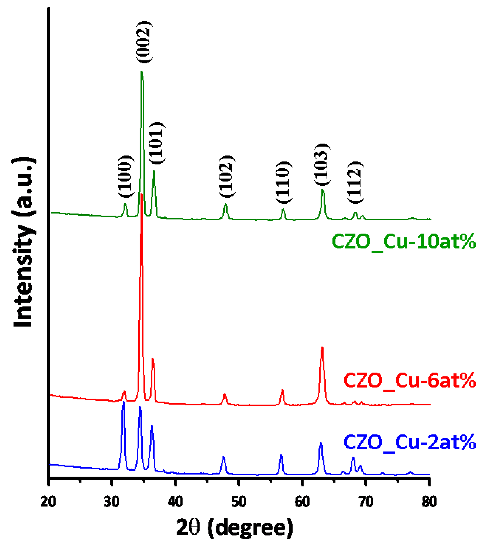
The XRD patterns of CZO thin films with various Cu-doping concentrations of 2%, 6%, and 10% are shown in Figure 1. The XRD results reveal that all CZO thin films have a wurtzite structured crystalline ZnO (JCPDS 36-1451) and have a significant (002) preferred orientation, which has been confirmed by a previous study [17]. No other phases corresponding to metal copper, oxides, or binary zinc copper were observed, indicating that Cu-doping is uniform and does not alter the hexagonal wurtzite structure of ZnO films. It is noted that the intensity of (002)-peak was enhanced dramatically when the Cu-doping concentration was increased from 2% to 6%. However, further increasing of the Cu-doping concentration up to 10% reduced the intensity of the (002)-peak, suggesting that excessive Cu-doping can degrade the (002) preferential orientation of CZO thin films. The crystalline size of CZO thin films was evaluated using the full-width at half-maximum (FWHM) of the (002)-peak according to Scherrer’s equation [26]:
where D is the crystalline size, λ is the wavelength of the X-ray radiation (Cu Kα, λ = 1.5406 Å), θ is the Bragg angle, and β is the line width of the (002) diffraction peak, respectively. Since broadening of diffraction lines may arise from the instrumental broadening and from the crystal size, structural defects, and residual strain of materials. The measured instrumental broadening of about 0.152°, by a Si standard sample, was then subtracted from the raw data while performing the crystallite size calculation. The derived crystalline size indicated that it increases from 20 to 50 nm and then decreases to 29 nm with the Cu-doping concentration of 2%, 6%, and 10%, respectively.
Moreover, in Figure 1, the diffraction angle of the (002) diffraction peak is found to shift to a higher angle with increasing Cu-doping concentrations, which suggests that the lattice constant (c) of CZO thin films is decreased according to the Bragg’s formula:
where d denotes the crystalline plane distance of indices (h, k, l). Since the Cu2+ ionic radius (0.73 Å) is smaller than that of the Zn2+ ion (0.74 Å) [15], it is expected that substitutional doping of Cu should slightly shrink the ZnO lattice and cause the (002)-peak to shift to a higher angle. From the obtained results, one may further estimate the induced stress in the CZO thin films using the following formula:
where c0 (=0.5205 nm) is the lattice constant of ZnO film without defects. The obtained stresses were 0.2238, 0.3581, and 0.5819 GPa for Cu-2%, Cu-6%, and Cu-10% doping in CZO thin films, respectively. Since the size of Cu2+ is smaller than that of the Zn2+, the resultant stresses are tensile.
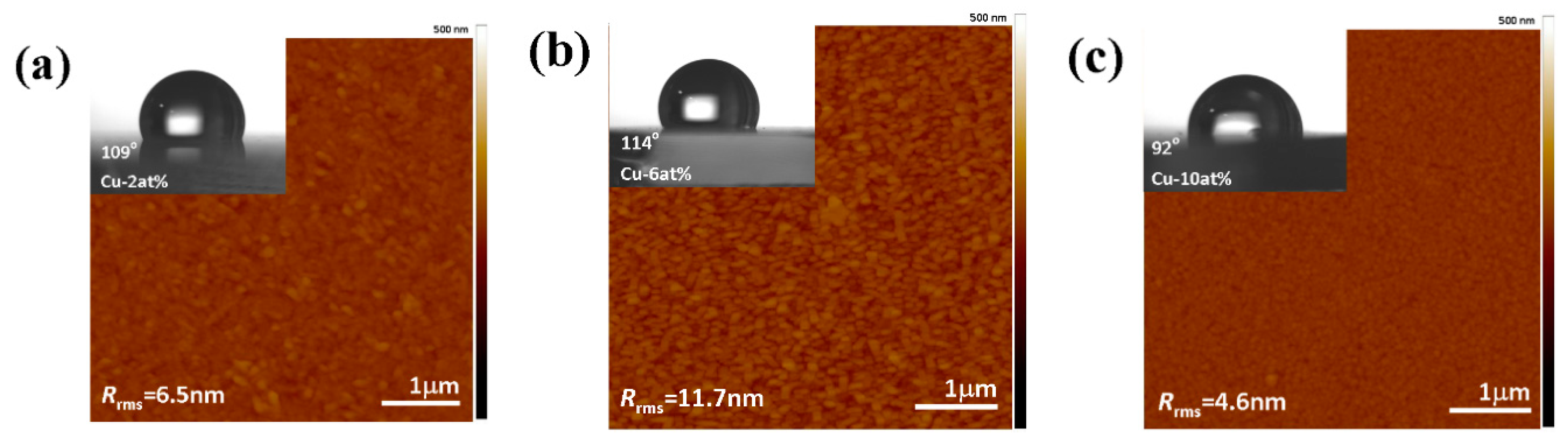
The surface morphologies of CZO thin films revealed by AFM observations are shown in Figure 2. It can be seen that the CZO thin films all exhibit dense and homogenous microstructures. The AFM analysis of the CZO thin films showed that the Rrms of films increased from Cu-2% to Cu-6% because of the increase in crystalline size. As a result, the film surface of the Cu-6% sample was also rougher. The Rrms of each respective CZO thin film is also displayed in Figure 2.
The wettability behavior of the surface is strongly related to the surface morphology of the sample surface [27]. The results of wettability tests are shown in the inset of Figure 2a–c. With an increasing Rrms, a larger amount of air is expected to be trapped in the gap of the nanoislands [28], which, in turn, would greatly increase the contact area of the air-water interface (i.e., preventing the water droplets from penetrating into the air pockets), resulting in a larger contact angle (θCA), as displayed in the rougher sample (see the Cu-6% doping CZO thin film in Figure 2b). It is noted that similar phenomena were reported by Dave et al. [29].
In general, the surface wettability is a measure of the surface energy and is most commonly quantified by θCA [18]. The surface energy for CZO thin films was calculated using the Fowkes-Girifalco-Good (FGG) theory [30]. According to the analysis of the FGG method, the considered critical interaction is the dispersive force or the van der Waals force across the interface existing between the water droplet and the solid surface. The FGG equation is given as:
where and are the dispersive portions of the surface tension for the liquid and solid surfaces, respectively. Using the Young’s equation [18] combined with Equation (4) and employing nonpolar liquid deionized water (72.8 mJ·m−2) as a testing liquid, is equal to , and the Girifalco-Good-Fowkes-Young equation becomes:
where is the surface energy of the calculated materials. Hence, by straightforward analyses, the values of the surface energy obtained for CZO thin film were 12.3, 10.8, and 17.5 mJ·m−2, respectively, for 2%, 6%, and 10% Cu-doping concentrations. Previous studies have indicated that the surface roughness is directly proportional to the contact angle and thereby inversely proportional to the surface energy of ZnO films [31,32]. Our results, nevertheless, are similar to that reported by Sapkal et al. [33]. In their work, the intensity of the (002) peak was significantly improved by an optimal Ag-doping concentration of ~3% in ZnO films, which evidently led to a larger θCA value. Based on these observations, it appears that the surface roughness and crystallinity of CZO thin films are the two main factors governing the surface wettability. In our case, an optimal doping concentration of Cu (~6%), seems to result in similar behaviors observed by Sapkal et al. [33]. Namely, the surface becomes much more hydrophobic (i.e., much lower surface energy) when the ZnO films are properly doped with Cu.
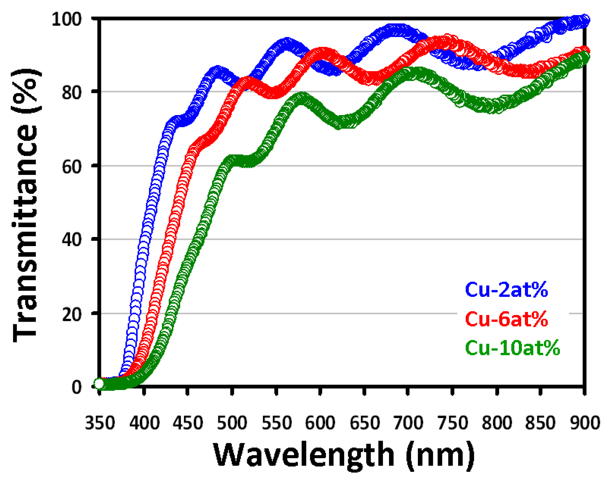
The optical transmittance spectra of CZO thin films with various Cu-doping concentrations of 2%, 6%, and 10% are displayed in Figure 3. As can be seen, the transmittance values are varied between 70% to 90% in the visible region (400–800 nm). It is clear from the transmittance spectra that the transparency has decreased with an increasing Cu-doping concentration, which is consistent with previous studies [34,35].
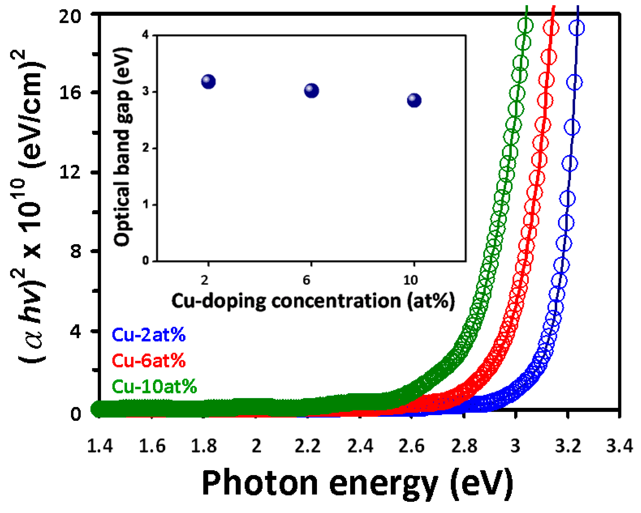
The influence of Cu-doping concentrations on the optical band gap (Eg) of CZO thin films can be further estimated from Figure 3. The Eg is calculated from transmittance data by using the Tauc equation:
where α is the absorption coefficient, hv is the photon energy, A is the constant, and n is an index. The index, n, can be 0.5 or 2 depending on whether it is a direct or indirect transition. Figure 4 shows a plot of the (αhv)2 versus the photon energy, which is linear at the absorption edge, confirming that the CZO films have a direct band gap. The value of the band gap is estimated by extrapolation of the straight line to the linear part to intersect the photon energy axis at Eg values. In the inset of Figure 4, it can be observed that the Eg of Cu-2% CZO film is 3.18 eV, while increasing the Cu concentration to 6% and 10% caused it to decrease to 3.02 and 2.85 eV, respectively. This is consistent with the XRD results because the tensile stress causes a red shift in the Eg values by increasing the Cu-doping concentration in CZO thin films [36]. According to a previous study [37], the Cu 3d orbital is much shallower than the Zn 3d orbital. The strong d-p coupling between Cu and O moves the O 2p up, while a Cu atom occupies a Zn site in ZnO, resulting in the narrowed direct band gap being exhibited. These facts may be related to the red shift of Eg values by Cu-doping in ZnO thin films.
4. Conclusions
In summary, we report the structural, surface morphological, optical, and wetting properties of CZO thin films with various Cu-doping concentrations grown by radio frequency magnetron sputtering technique. XRD results indicated that CZO thin films had a hexagonal wurtzite structure and exhibited a (002)-preferred orientation. AFM observations showed that the surface morphological properties were changed via Cu doping and a larger crystalline size (28 nm) was presented in Cu-6% doping of CZO films. All CZO thin films exhibited a transmittance of over 80% in the visible wavelength range. Moreover, the optical energy band gap of CZO thin films shifted from 3.18 to 2.85 eV with increasing Cu-doping concentrations from 2% to 10%. Combined with the contact angle measurement and theory calculation, all CZO thin films exhibited a low surface energy, resulting in hydrophobic behaviors.
Author Contributions
G.-J.C. contributed to the experiments and analyses. S.-R.J. and J.-Y.J. contributed to the discussion on materials characterizations. S.-R.J. designed the project of experiments and drafted the manuscript. All authors read and approved the final manuscript.
Funding
This research was funded by the Ministry of Science and Technology, Taiwan under Contract Nos., MOST104-2221-E-214-003, MOST105-2112-M-214-001, MOST106-2112-M-214-001 and MOST106-2221-E-214-014.
Acknowledgments
The authors thank H.-C. Tseng and C.-F. Wang for their technical support.
Conflicts of Interest
The authors declare no conflict of interest.
References
- Chu, S.; Wang, G.; Zhou, W.; Lin, Y.; Chernyak, L.; Zhao, J.; Kong, J.; Li, L.; Ren, J.; Liu, J. Electrically pumped waveguide lasing from ZnO nanowires. Nat. Nanotechnol. 2011, 6, 506–510. [Google Scholar] [CrossRef] [PubMed]
- Wang, C.F.; Ba, R.R.; Zhao, K.; Zhang, T.P.; Dong, L.; Pan, C.F. Enhanced emission intensity of vertical aligned flexible ZnO nanowire/p-polymer hybridized LED array by piezo-phototronic effect. Nano Energy 2015, 14, 364–371. [Google Scholar] [CrossRef]
- Liu, X.H.; Wang, H.Q.; Li, Y.R.; Gui, Z.Z.; Ming, S.Q.; Usman, K.; Zhang, W.J.; Fang, J.F. Regular Organic Solar Cells with Efficiency over 10% and Promoted Stability by Ligand- and Thermal Annealing-Free Al-Doped ZnO Cathode Interlayer. Adv. Sci. 2017, 4, 1700053. [Google Scholar] [CrossRef] [PubMed] [Green Version]
- Li, Y.; Yao, R.; Wang, H.H.; Wu, X.M.; Wu, J.Z.; Wu, X.H.; Qin, W. Enhanced Performance in Al-Doped ZnO Based Transparent Flexible Transparent Thin-Film Transistors Due to Oxygen Vacancy in ZnO Film with Zn–Al–O Interfaces Fabricated by Atomic Layer Deposition. ACS Appl. Mater. Interfaces 2017, 9, 11711–11720. [Google Scholar] [CrossRef] [PubMed]
- Yeh, P.H.; Li, Z.; Wang, Z.L. Schottky-Gated Probe-Free ZnO Nanowire Biosensor. Adv. Mater. 2009, 21, 4975–4978. [Google Scholar] [CrossRef] [PubMed]
- Park, C.H.; Zhang, S.B.; Wei, S.H. Origin of p-type doping difficulty in ZnO: The impurity perspective. Phys. Rev. B 2002, 66, 073202. [Google Scholar] [CrossRef]
- Look, D.C.; Jones, R.L.; Sizelove, J.R.; Garces, N.Y.; Giles, C.N.; Halliburton, L.E. The path to ZnO devices: Donor and acceptor dynamics. Phys. Status Solidi A 2003, 195, 171–177. [Google Scholar] [CrossRef]
- Look, D.C.; Clafin, B. P-type doping and devices based on ZnO. Phys. Status Solidi B 2004, 241, 624–630. [Google Scholar] [CrossRef]
- Shi, S.W.; He, G.; Zhang, M.; Song, X.P.; Li, J.L.; Wang, X.X.; Cui, J.B.; Chen, X.S.; Sun, Z.Q. Microstructural, Optical and Electrical Properties of Molybdenum Doped ZnO Films Deposited by Magnetron Sputtering. Sci. Adv. Mater. 2012, 4, 193–198. [Google Scholar] [CrossRef]
- Lee, D.J.; Kim, K.J.; Kim, S.H.; Kwon, J.Y.; Xu, J.; Kim, K.B. Atomic layer deposition of Ti-doped ZnO films with enhanced electron mobility. J. Mater. Chem. C 2013, 1, 4761–4769. [Google Scholar] [CrossRef]
- Liu, H.; Yang, J.; Hua, Z.; Zhang, Y.; Yang, L.; Xiao, L.; Xie, Z. The structure and magnetic properties of Cu-doped ZnO prepared by sol–gel method. Appl. Surf. Sci. 2010, 256, 4162–4165. [Google Scholar] [CrossRef]
- Allabergenov, B.; Chung, S.H.; Jeong, S.M.; Kim, S.; Choi, B. Enhanced blue photoluminescence realized by copper diffusion doping of ZnO thin films. Opt. Mater. Express 2013, 3, 1733–1741. [Google Scholar] [CrossRef]
- Ashokkumar, M.; Muthukumaran, S. Effect of Ni doping on electrical, photoluminescence and magnetic behavior of Cu doped ZnO nanoparticles. J. Lumin. 2015, 162, 97–103. [Google Scholar] [CrossRef]
- Iikhechi, N.N.; Ghobadi, N.; Yahyavi, F. Enhanced optical and hydrophilic properties of V and La co-doped ZnO thin films. Opt. Quant. Electron. 2017, 49, 39. [Google Scholar] [CrossRef]
- Wu, Z.F.; Wu, X.M.; Zhuge, L.J. Synthesis and magnetic properties of Cu doped ZnO nanorods via radio frequency plasma deposition. Appl. Phys. Lett. 2008, 93, 023103. [Google Scholar] [CrossRef]
- Zimmermann, J.; Reifler, F.A.; Schrade, U.; Artus, G.R.J.; Seeger, S. Long term environmental durability of a superhydrophobic silicone nanofilament coating. Colloids Surf. A Physicochem. Eng. Asp. 2007, 302, 234–240. [Google Scholar] [CrossRef]
- Tyona, M.D.; Osuji, R.U.; Asogwa, P.U.; Jambure, S.B.; Ezema, F.I. Structural modification and band gap tailoring of zinc oxide thin films using copper impurities. J. Solid State Electrochem. 2017, 21, 2629–2637. [Google Scholar] [CrossRef]
- Angelo, M.S.; McCandless, B.E.; Birkmire, R.W.; Rykov, S.A.; Chen, J.G. Contact wetting angle as a characterization technique for processing CdTe/CdS solar cells. Prog. Photovolt. 2007, 15, 93–111. [Google Scholar] [CrossRef]
- Sun, H.; Luo, M.; Weng, W.; Cheng, K.; Du, P.; Shen, G.; Han, G. Room-temperature preparation of ZnO nanosheets grown on Si substrates by a seed-layer assisted solution route. Nanotechnology 2008, 19, 125603. [Google Scholar] [CrossRef] [PubMed]
- Shinde, S.K.; Ghodake, G.S.; Dubal, D.P.; Lohar, G.M.; Lee, D.S.; Fulari, V.J. Structural, optical, and photo-electrochemical properties of marygold-like CdSe0.6Te0.4 synthesized by electrochemical route. Ceram. Int. 2014, 40, 11519–11524. [Google Scholar] [CrossRef]
- Hashim, N.H.; Subramani, S.; Devarajan, M.; Ibrahim, A.R. Structural and surface characterization of undoped ZnO and Cu doped ZnO using sol–gel spin coating method. J. Mater. Sci. Mater. Electron. 2016, 27, 3520–3530. [Google Scholar] [CrossRef]
- Suja, M.; Bashar, S.B.; Morshed, M.M.; Liu, J.L. Realization of Cu-Doped p-Type ZnO Thin Films by Molecular Beam Epitaxy. ACS Appl. Mater. Interfaces 2015, 7, 8894–8899. [Google Scholar] [CrossRef] [PubMed]
- Shewale, P.S.; Yu, Y.S. UV photodetection properties of pulsed laser deposited Cu-doped ZnO thin film. Ceram. Int. 2017, 43, 4175–4182. [Google Scholar] [CrossRef]
- Xu, S.S.; Lu, H.L.; Zhang, Y.; Wang, T.; Geng, Y.; Huang, W.; Ding, S.J.; Zhang, D.W. Bandgap narrowing and conductivity evolution of atomic-layer-deposited ZnO:Cu thin films under rapid thermal annealing. J. Alloys Compd. 2015, 638, 133–135. [Google Scholar] [CrossRef]
- Sreedhar, A.; Kwon, J.H.; Yi, J.; Kim, J.S.; Gwag, J.S. Enhanced photoluminescence properties of Cu-doped ZnO thin films deposited by simultaneous RF and DC magnetron sputtering. Mater. Sci. Semcond. Process. 2016, 49, 8–14. [Google Scholar] [CrossRef]
- Cullity, B.D.; Stock, S.R. Element of X-ray Diffraction; Prentice Hall: New Jersey, NJ, USA, 2001; p. 170. [Google Scholar]
- Ottone, C.; Lamberti, A.; Cauda, V.; Fontana, M. Wetting Behavior of Hierarchical Oxide Nanostructures: TiO2 Nanotubes from Anodic Oxidation Decorated with ZnO Nanostructures. J. Electrochem. Soc. 2014, 161, D484–D488. [Google Scholar] [CrossRef]
- Bayati, R.; Molaei, R.; Richmond, A.; Nori, S.; Wu, F.; Kumar, D.; Narayan, J.; Reynolds, J.G.; Reynolds, C.L. Modification of Properties of Yttria Stabilized Zirconia Epitaxial Thin Films by Excimer Laser Annealing. ACS Appl. Mater. Interfaces 2014, 6, 22316. [Google Scholar] [CrossRef] [PubMed]
- Dave, V.; Gupta, H.O.; Chandra, R. Nanostructured hydrophobic DC sputtered inorganic oxide coating for outdoor glass insulators. Appl. Surf. Sci. 2014, 295, 231–239. [Google Scholar] [CrossRef]
- Mahadik, D.B.; Rao, A.V.; Parale, V.G.; Kavale, M.S.; Wagh, P.B.; Ingale, S.V.; Gupta, S.C. Effect of surface composition and roughness on the apparent surface free energy of silica aerogel materials. Appl. Phys. Lett. 2011, 99, 104104. [Google Scholar] [CrossRef]
- Chi, P.W.; Wei, D.H.; Wu, S.H.; Chen, Y.Y.; Yao, Y.D. Photoluminescence and wettability control of NiFe/ZnO heterostructure bilayer films. RSC Adv. 2015, 5, 96705–96713. [Google Scholar] [CrossRef]
- Chao, C.H.; Chi, P.W.; Wei, D.H. Investigations on the Crystallographic Orientation Induced Surface Morphology Evolution of ZnO Thin Films and Their Wettability and Conductivity. J. Phys. Chem. C 2016, 120, 8210–8219. [Google Scholar] [CrossRef]
- Sapkal, R.T.; Shinde, S.S.; Babar, A.R.; Moholkar, A.V.; Rajpure, K.Y.; Bhosale, C.H. Structural, Morphological, Optical and Photoluminescence Properties of Ag-Doped Zinc Oxide Thin Films. Mater. Express 2012, 2, 64–70. [Google Scholar] [CrossRef]
- Ghosh, T.; Dutta, M.; Mridha, S.; Basak, D. Effect of Cu Doping in the Structural, Electrical, Optical, and Optoelectronic Properties of Sol-Gel ZnO Thin Films. J. Electrochem. Soc. 2009, 156, H285–H289. [Google Scholar] [CrossRef]
- Saritha, A.C.; Shijeesh, M.R.; Vikas, L.S.; Prabhu, R.R.; Jayara, M.K. Growth and characterization of p-ZnO:Cu thin film and its homojunction application. J. Phys. D Appl. Phys. 2016, 49, 295105. [Google Scholar] [CrossRef]
- Rao, T.P.; Kumar, M.C.S.; Angayarkanni, S.A.; Ashok, M. Effect of stress on optical band gap of ZnO thin films with substrate temperature by spray pyrolysis. J. Alloys Compd. 2009, 485, 413–417. [Google Scholar] [CrossRef]
- Ahn, K.S.; Deutsch, T.; Yan, Y.; Jiang, C.S.; Perkins, C.L.; Turner, J.; Al-Jassim, M. Synthesis of band-gap-reduced p-type ZnO films by Cu incorporation. J. Appl. Phys. 2007, 102, 023517. [Google Scholar] [CrossRef]
Figure 1.
X-ray diffraction (XRD) patterns of CZO thin films deposited on glass substrates with various Cu-doping concentrations.
Figure 1.
X-ray diffraction (XRD) patterns of CZO thin films deposited on glass substrates with various Cu-doping concentrations.

Figure 2.
atomic force microscopy (AFM) surface micrographs (5 × 5 µm2) of CZO thin films with various Cu-doping concentrations (a) 2%, (b) 6%, and (c) 10%. Inset: The corresponding water contact angles.
Figure 2.
atomic force microscopy (AFM) surface micrographs (5 × 5 µm2) of CZO thin films with various Cu-doping concentrations (a) 2%, (b) 6%, and (c) 10%. Inset: The corresponding water contact angles.

Figure 3.
UV-Vis transmittance spectra of CZO thin films with various Cu-doping concentrations.

Figure 4.
Plots of (αhv)2 versus photon energy of CZO thin films with various Cu-doping concentrations. Inset: The evaluated optical band gap of CZO thin films.
Figure 4.
Plots of (αhv)2 versus photon energy of CZO thin films with various Cu-doping concentrations. Inset: The evaluated optical band gap of CZO thin films.


Table 1.
The composition of CZO thin films measured by X-ray photoelectron spectroscopy (XPS).
| Sample | Cu (at %) | Zn (at %) | O (at %) | Stoichiometry of Cu |
|---|---|---|---|---|
| 2% | 1.1 | 47.96 | 50.94 | 0.022 |
| 6% | 3.31 | 46.32 | 50.37 | 0.067 |
| 10% | 5.48 | 43.24 | 51.28 | 0.112 |
© 2018 by the authors. Licensee MDPI, Basel, Switzerland. This article is an open access article distributed under the terms and conditions of the Creative Commons Attribution (CC BY) license (http://creativecommons.org/licenses/by/4.0/).
Share and Cite
MDPI and ACS Style
Chen, G.-J.; Jian, S.-R.; Juang, J.-Y. Surface Analysis and Optical Properties of Cu-Doped ZnO Thin Films Deposited by Radio Frequency Magnetron Sputtering. Coatings 2018, 8, 266. https://doi.org/10.3390/coatings8080266
AMA Style
Chen G-J, Jian S-R, Juang J-Y. Surface Analysis and Optical Properties of Cu-Doped ZnO Thin Films Deposited by Radio Frequency Magnetron Sputtering. Coatings. 2018; 8(8):266. https://doi.org/10.3390/coatings8080266
Chicago/Turabian StyleChen, Guo-Ju, Sheng-Rui Jian, and Jenh-Yih Juang. 2018. "Surface Analysis and Optical Properties of Cu-Doped ZnO Thin Films Deposited by Radio Frequency Magnetron Sputtering" Coatings 8, no. 8: 266. https://doi.org/10.3390/coatings8080266
Note that from the first issue of 2016, this journal uses article numbers instead of page numbers. See further details here.