Investigation of TiO2 Thin Film Deposited by Microwave Plasma Assisted Sputtering and Its Application in 3D Glasses

 , , ,
, , ,
Abstract
:1. Introduction
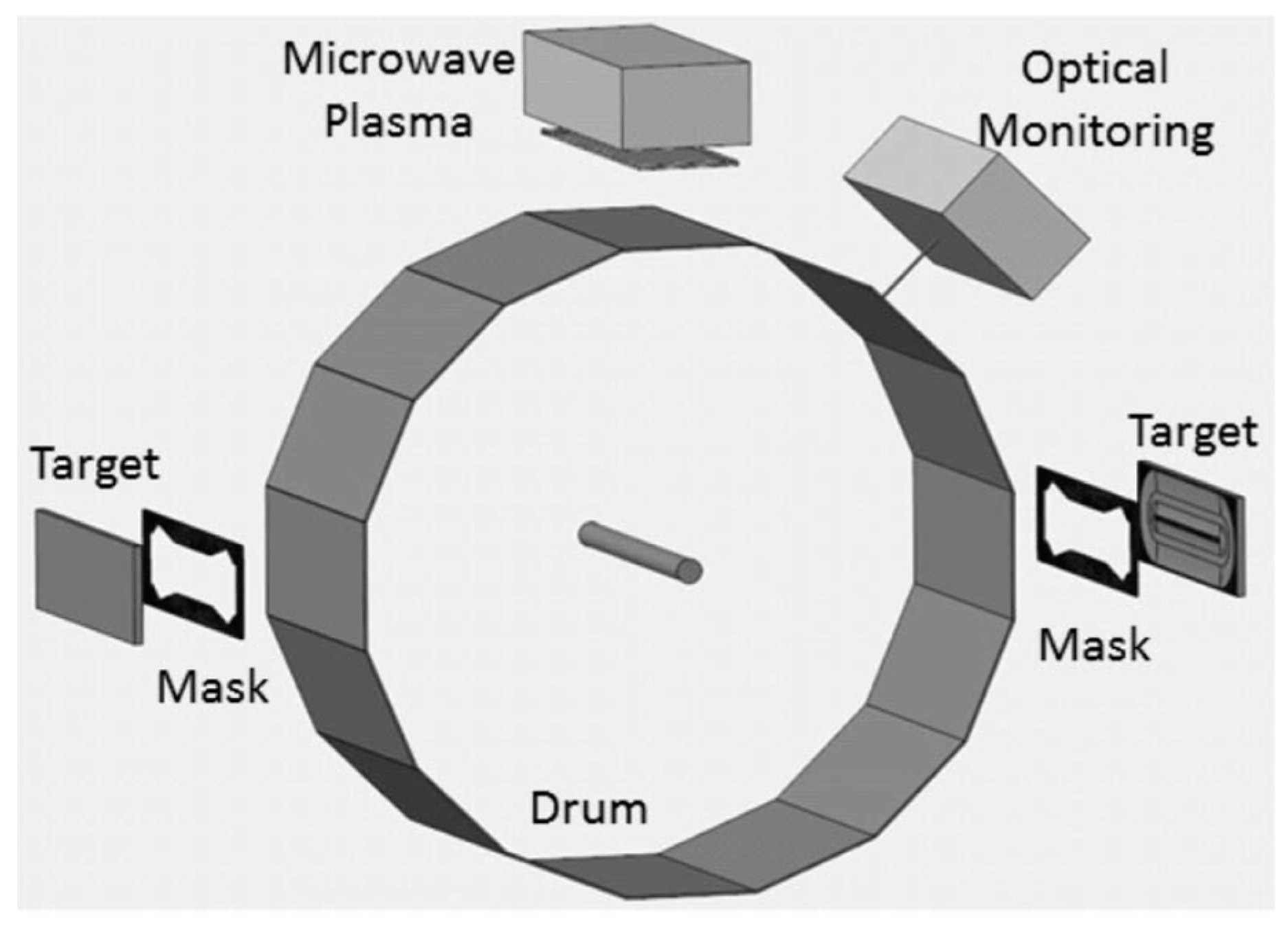
2. Experiments
3. Thin Film Modelling and Interference Filter Design
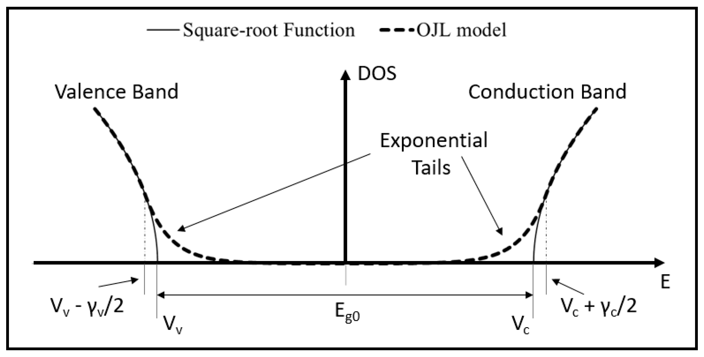
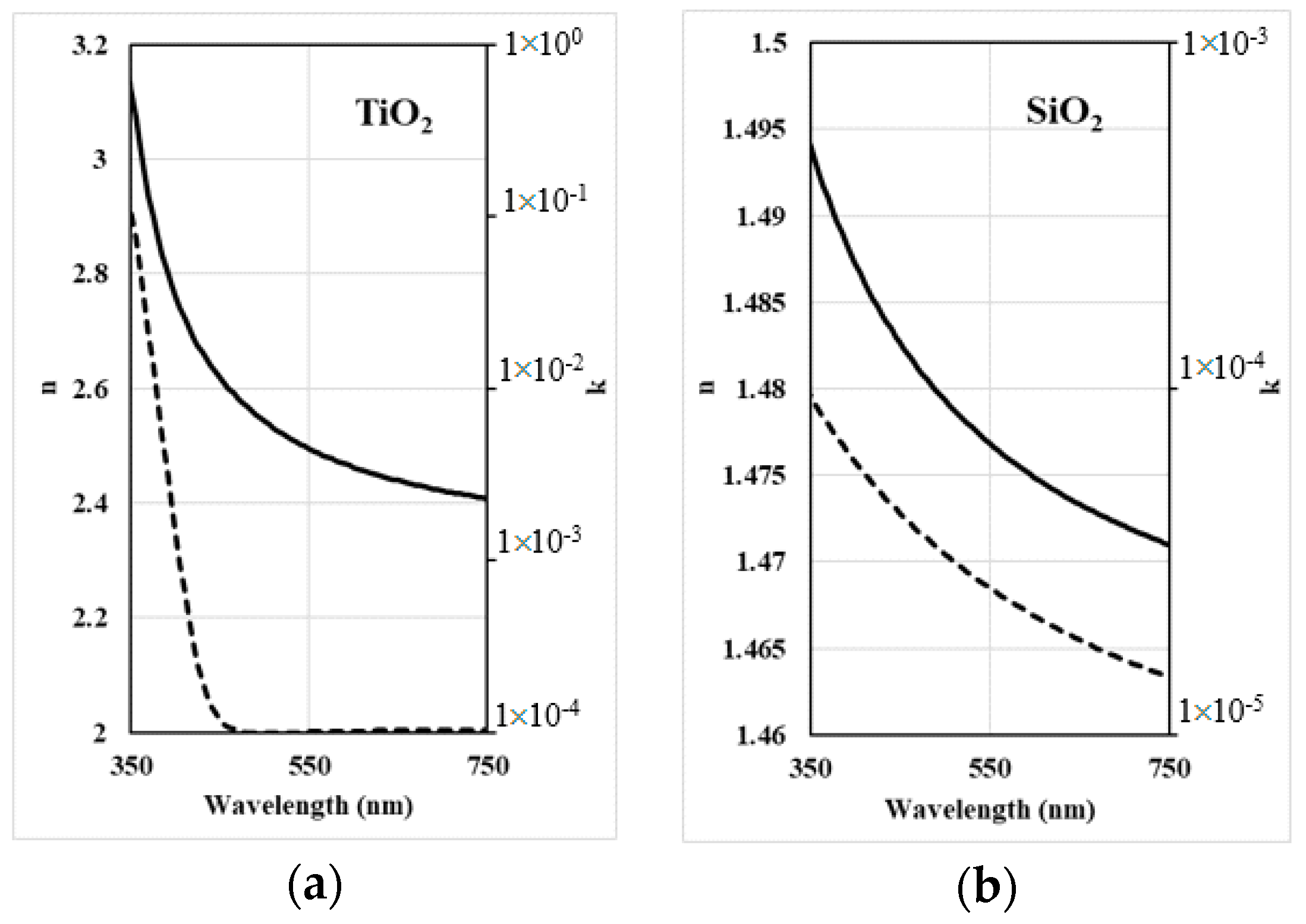
3.1. Dispersive Model Used for Transmittance Fitting
3.2. Rough Surface and Light Scattering
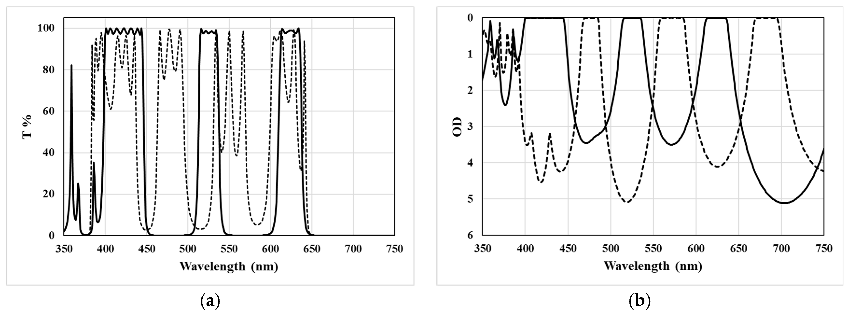
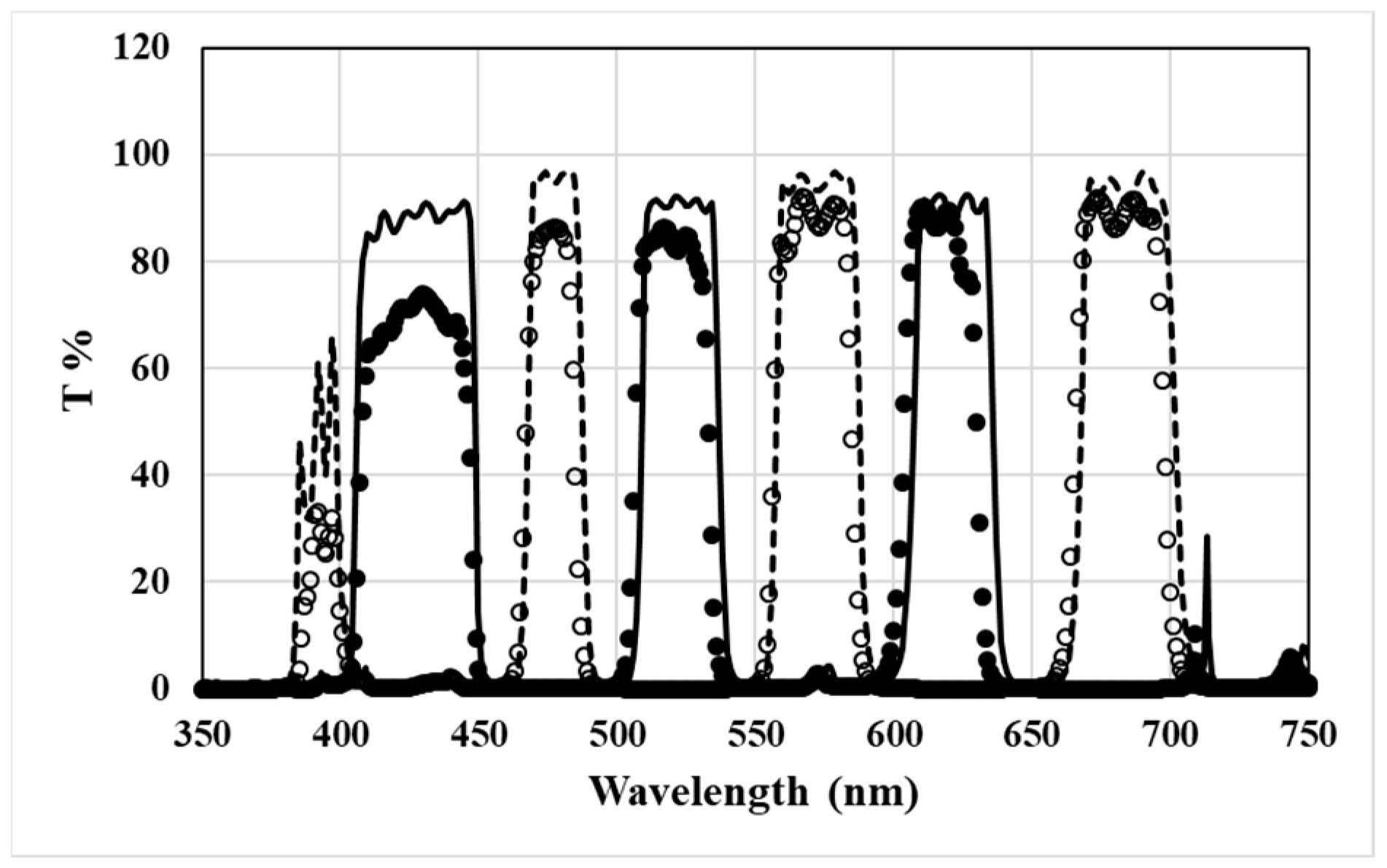
3.3. Design of Triple Bandpass Filter for 3D Glasses
4. Results and Discussions
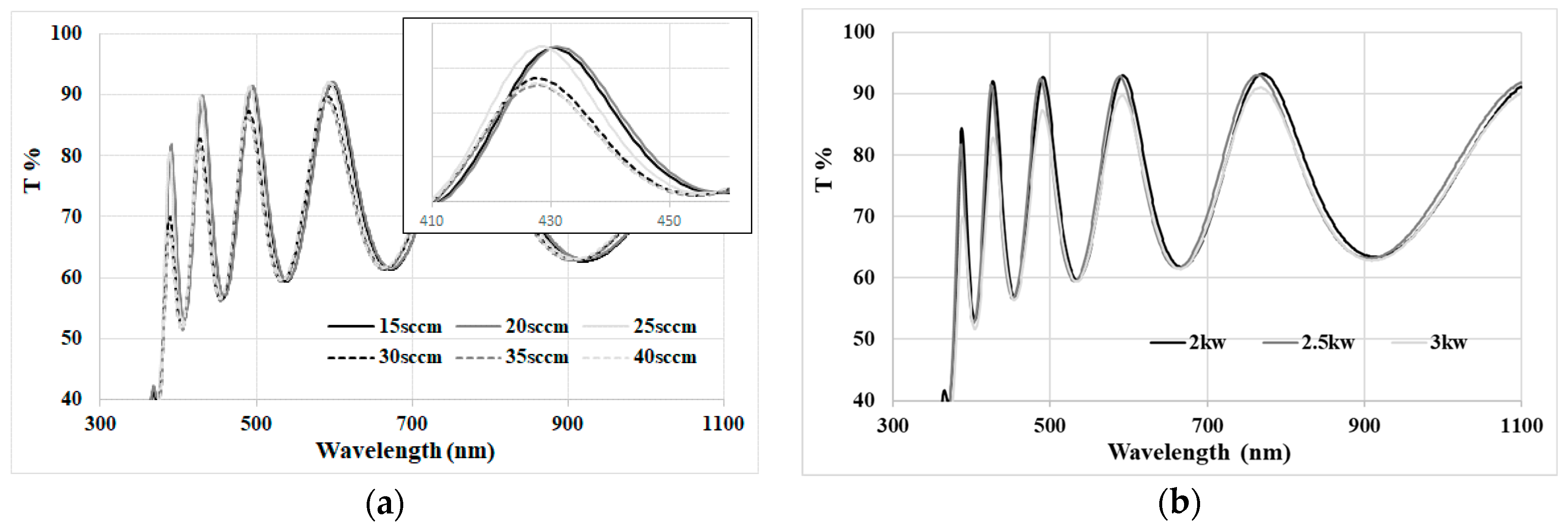
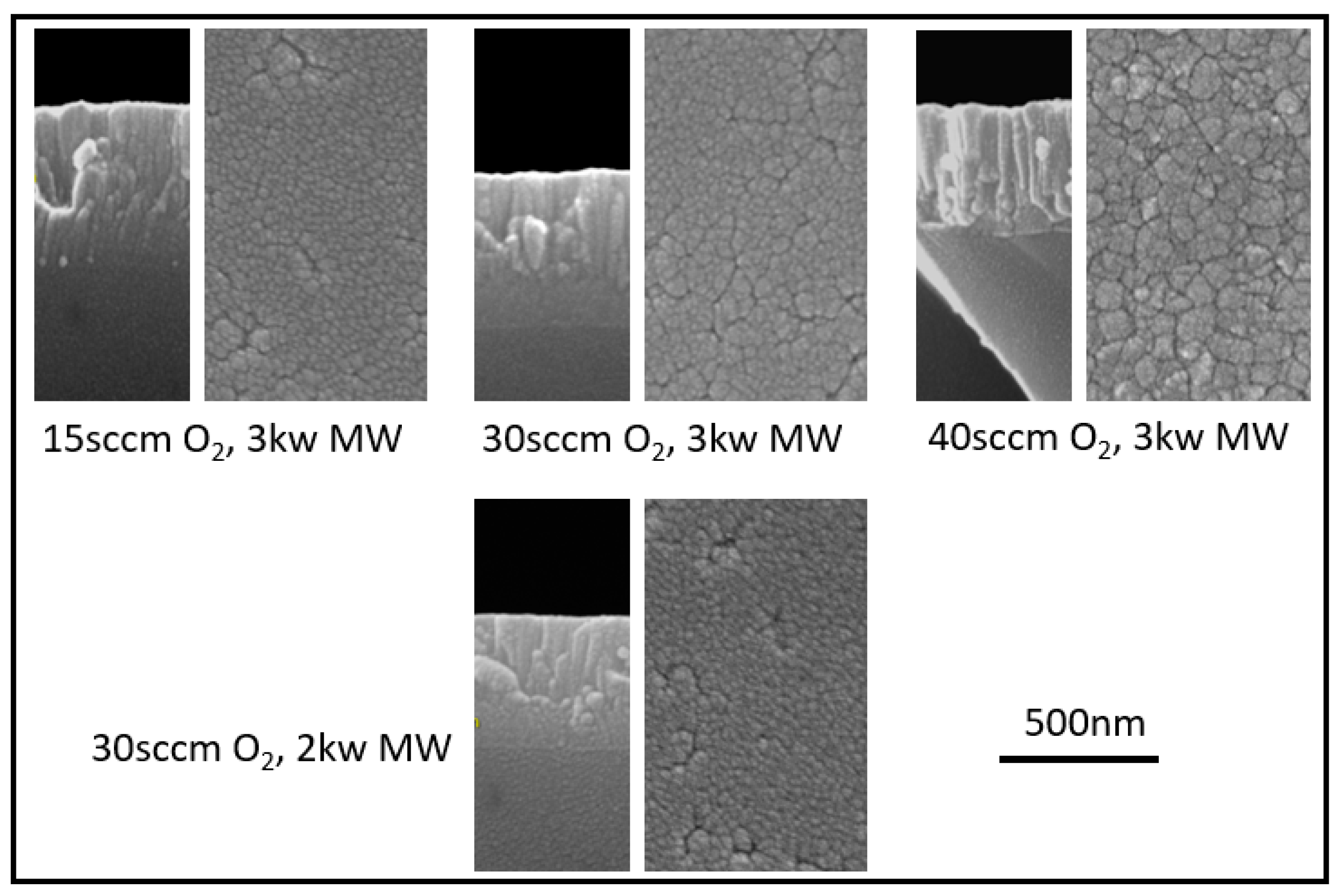
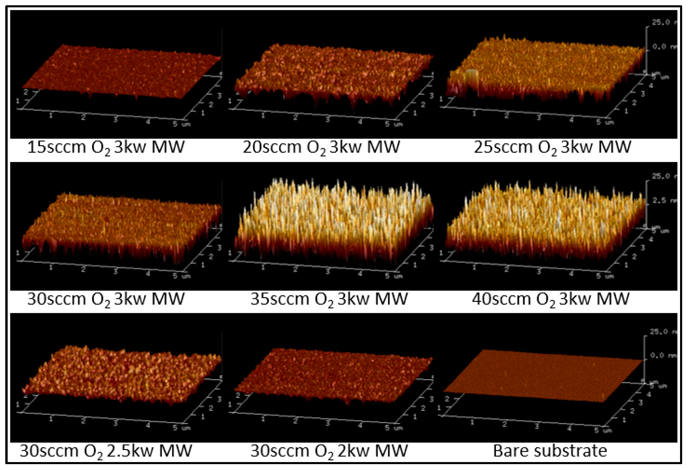
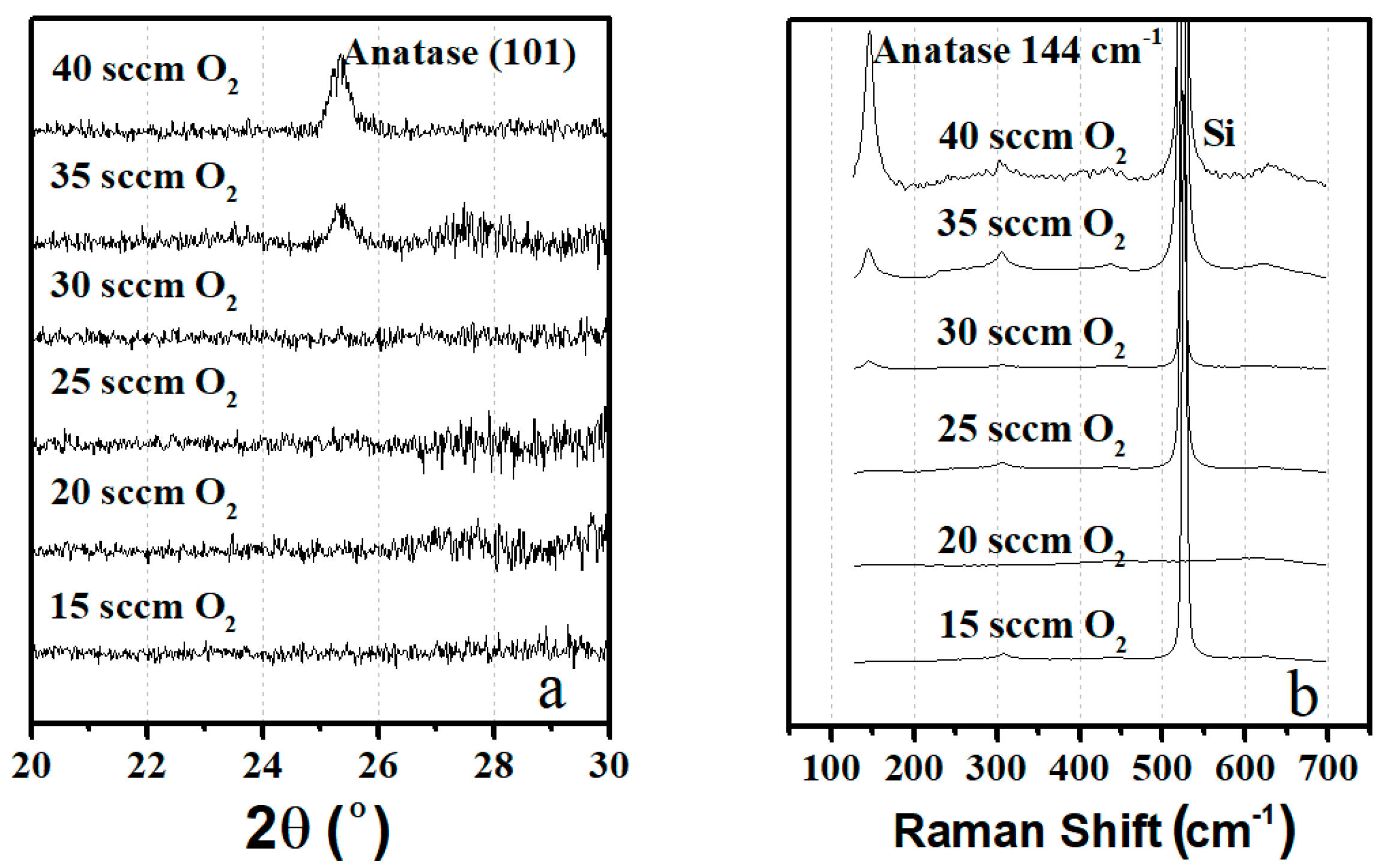
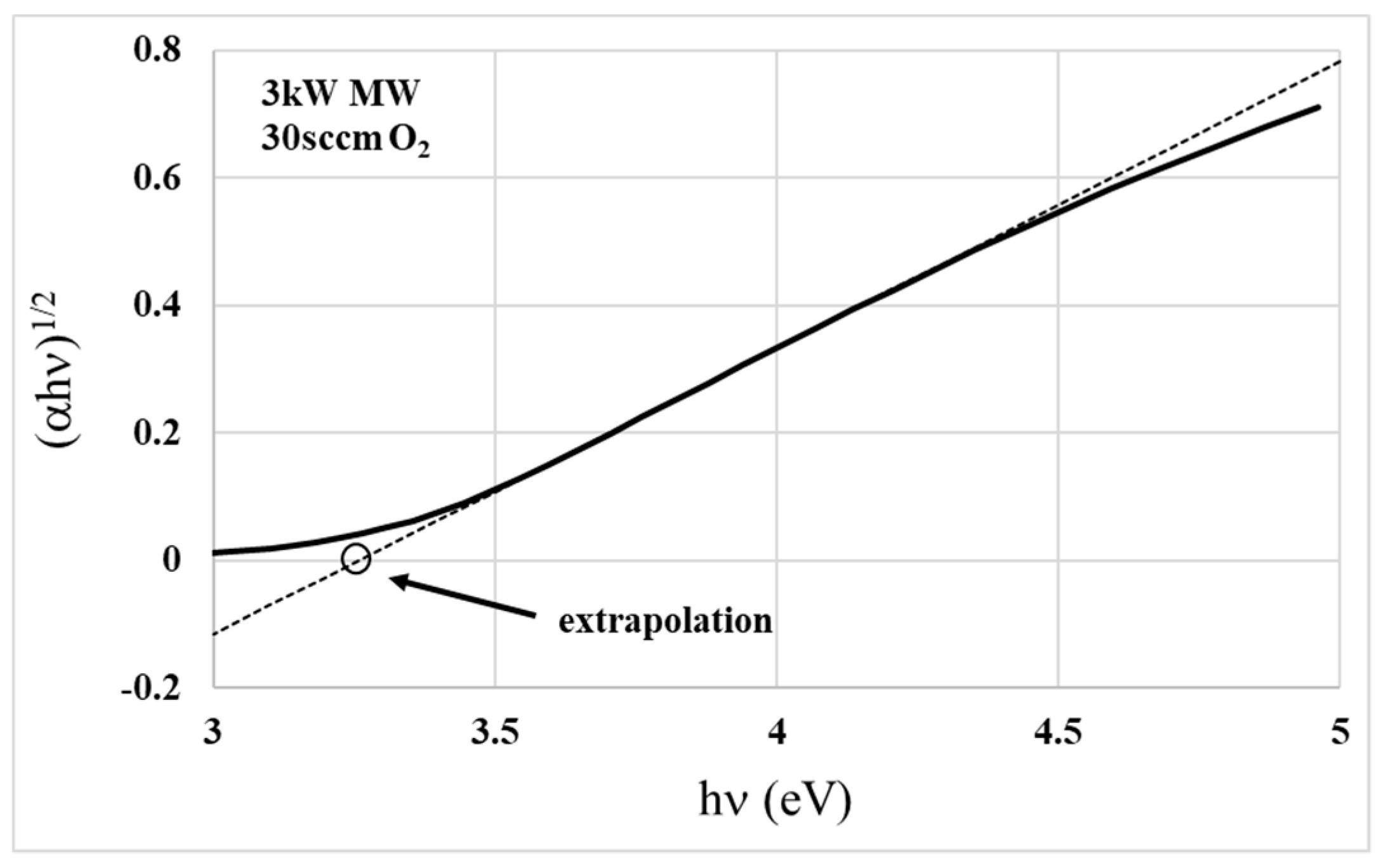
4.1. TiO2 Thin Film Process Optimization
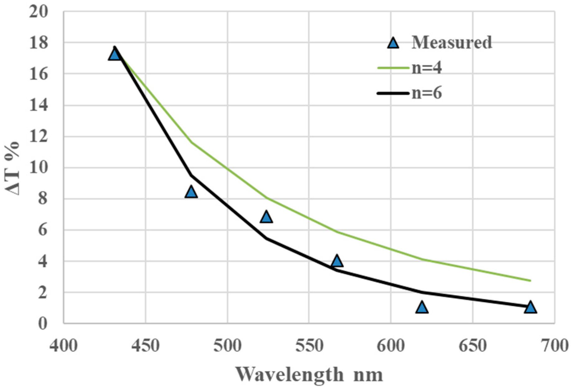
4.2. Fabrication of 3D Glasses Filter
5. Conclusions
Author Contributions
Funding
Conflicts of Interest
References
- Selopal, G.S.; Wu, H.-P.; Lu, J.; Chang, Y.-C.; Wang, M.; Vomiero, A.; Concina, I.; Diau, E.W.G. Metal-free organic dyes for TiO2 and ZnO dye-sensitized solar cells. Sci. Rep. 2016, 6, 18756. [Google Scholar] [CrossRef] [PubMed]
- Schneider, J.; Matsuoka, M.; Takeuchi, M.; Zhang, J.; Horiuchi, Y.; Anpo, M.; Bahnemann, D.W. Understanding TiO2 photocatalysis: Mechanisms and materials. Chem. Rev. 2014, 114, 9919–9986. [Google Scholar] [CrossRef] [PubMed]
- Tang, H.; Prasad, K.; Sanjinés, R.; Lévy, F. TiO2 anatase thin films as gas sensors. Sens. Actuators B Chem. 1995, 26, 71–75. [Google Scholar] [CrossRef]
- Keshavarz Hedayati, M.; Elbahri, M. Antireflective coatings: Conventional stacking layers and ultrathin plasmonic metasurfaces, a mini-review. Materials 2016, 9, 497. [Google Scholar] [CrossRef] [PubMed]
- Lam, S.W.; Gan, W.Y.; Chiang, K.; Amal, R. TiO2 semiconductor—A smart self-cleaning material. J. Aust. Ceram. Soc. 2008, 44, 6–11. [Google Scholar]
- Verdier, T.; Coutand, M.; Bertron, A.; Roques, C. Antibacterial activity of TiO2 photocatalyst alone or in coatings on E. coli: The influence of methodological aspects. Coatings 2014, 4, 670–686. [Google Scholar] [CrossRef]
- Tang, H.; Prasad, K.; Sanjinès, R.; Schmid, P.E.; Lévy, F. Electrical and optical properties of TiO2 anatase thin films. J. Appl. Phys. 1994, 75, 2042–2047. [Google Scholar] [CrossRef]
- Mo, S.-D.; Ching, W.Y. Electronic and optical properties of three phases of titanium dioxide: Rutile, anatase, and brookite. Phys. Rev. B 1995, 51, 13023–13032. [Google Scholar] [CrossRef]
- Chen, Q.; Qian, Y.; Chen, Z.; Wu, W.; Chen, Z.; Zhou, G.; Zhang, Y. Hydrothermal epitaxy of highly oriented TiO2 thin films on silicon. Appl. Phys. Lett. 1995, 66, 1608–1610. [Google Scholar] [CrossRef]
- Li, P.-Y.; Liu, H.-W.; Chen, T.-H.; Chang, C.-H.; Lu, Y.-S.; Liu, D.-S. Characterization of an amorphous titanium oxide film deposited onto a nano-textured fluorination surface. Materials 2016, 9, 429. [Google Scholar] [CrossRef] [PubMed]
- Zabihi, F.; Ahmadian-Yazdi, M.-R.; Eslamian, M. Photocatalytic graphene-TiO2 thin films fabricated by low-temperature ultrasonic vibration-assisted spin and spray coating in a sol-gel process. Catalysts 2017, 7, 136. [Google Scholar] [CrossRef]
- Niemelä, J.-P.; Marin, G.; Karppinen, M. Titanium dioxide thin films by atomic layer deposition: A review. Semicond. Sci. Technol. 2017, 32, 093005. [Google Scholar] [CrossRef]
- Murugesan, S.; Kuppusami, P.; Parvathavarthini, N.; Mohandas, E. Pulsed laser deposition of anatase and rutile TiO2 thin films. Surf. Coat. Technol. 2007, 201, 7713–7719. [Google Scholar] [CrossRef]
- Xiao, R.-F.; Ming, N.-B. Surface roughening and surface diffusion in kinetic thin-film deposition. Phys. Rev. E 1994, 49, 4720–4723. [Google Scholar] [CrossRef] [Green Version]
- Mehrabi, M.; Peek, E.M.; Wuensche, B.C.; Lutteroth, C. Making 3D work: A classification of visual depth cues, 3D display technologies and their applications. In Proceedings of the Fourteenth Australasian User Interface Conference, Adelaide, Australia, 29 January–1 February 2013. [Google Scholar]
- Holliman, N.S.; Dodgson, N.A.; Favalora, G.E.; Pockett, L. Three-dimensional displays: A review and applications analysis. IEEE Trans. Broadcast. 2011, 57, 362–371. [Google Scholar] [CrossRef]
- Simon, A.; Prager, M.G.; Schwarz, S.; Fritz, M.; Jorke, H. Interference-filter-based stereoscopic 3D LCD. J. Inf. Disp. 2010, 11, 22–27. [Google Scholar] [CrossRef]
- Reiners, D.; Rains, D.R.; Burgess, W.; Cruz-Neira, C. Laser illuminated projectors and their benefits for immersive environments. Electron. Imaging 2017, 2017, 42–47. [Google Scholar] [CrossRef]
- Jorke, H.; Simon, A. New high efficiency interference filter characteristics for stereoscopic imaging. In Stereoscopic Displays and Applications XXIII, Proceedings of IS&T/SPIE Electronic Imaging 2012, Burlingame, CA, USA, 22–26 January 2012; Woods, A.J., Holliman, N.S., Favalora, G.E., Eds.; International Society for Optics and Photonics: Bellingham, WA, USA, 2012. [Google Scholar]
- Song, S.; Li, C.; Chu, H.O.; Gibson, D. Reactive dynamics analysis of critical Nb2O5 sputtering rate for drum-based metal-like deposition. Appl. Opt. 2017, 56, C206. [Google Scholar] [CrossRef] [PubMed]
- O’Leary, S.K.; Johnson, S.R.; Lim, P.K. The relationship between the distribution of electronic states and the optical absorption spectrum of an amorphous semiconductor: An empirical analysis. J. Appl. Phys. 1998, 82, 3334–3340. [Google Scholar] [CrossRef]
- Tauc, J.; Grigorovici, R.; Vancu, A. Optical properties and electronic structure of amorphous germanium. Phys. Status Solidi 1966, 15, 627–637. [Google Scholar] [CrossRef]
- Tauc, J. Optical properties of amorphous semiconductors. In Amorphous and Liquid Semiconductors; Springer: Boston, MA, USA, 1974; pp. 159–220. [Google Scholar]
- Rakels, J.H. Influence of the surface height distribution on the total integrated scatter (TIS) formula. Nanotechnology 1996, 7, 43–46. [Google Scholar] [CrossRef]
- Chen, J.Y.; Sun, K.W. Nanostructured thin films for anti-reflection applications. Thin Solid Films 2011, 519, 5194–5198. [Google Scholar] [CrossRef]
- Stroud, D. The effective medium approximations: Some recent developments. Superlattices Microstruct. 1998, 23, 567–573. [Google Scholar] [CrossRef] [Green Version]
- Macleod, H.A. Band-pass filters. In Thin-Film Optical Filters, 3rd ed.; Institute of Physics Publishing: Bristol, UK, 2001; p. 257. ISBN 0750306882. [Google Scholar]
- Rafieian, D.; Ogieglo, W.; Savenije, T.; Lammertink, R.G.H. Controlled formation of anatase and rutile TiO2 thin films by reactive magnetron sputtering. AIP Adv. 2015, 5, 097168. [Google Scholar] [CrossRef]
- Sánchez, C.; Enrique, C. Quantification of phase content in TiO2 thin films by Raman spectroscopy. Superf. Vacío 2014, 27, 88–92. [Google Scholar]
- SHarvey, J.; Schröder, S.; Choi, N.; Duparré, A. Total integrated scatter from surfaces with arbitrary roughness, correlation widths, and incident angles. Opt. Eng. 2012, 51, 013402. [Google Scholar] [CrossRef]


| Sample | MW Power (kW) | O2 Flow (sccm) |
|---|---|---|
| 1 | 3 | 15 |
| 2 | 3 | 20 |
| 3 | 3 | 25 |
| 4 | 3 | 30 |
| 5 | 3 | 35 |
| 6 | 3 | 40 |
| 7 | 2.5 | 30 |
| 8 | 2 | 30 |
| MW Power (kW) | O2 Flow (sccm) | Roughness (Rq) (nm) |
|---|---|---|
| 3 | 15 | 0.94 |
| 3 | 20 | 3.07 |
| 3 | 25 | 4.13 |
| 3 | 30 | 4.61 |
| 3 | 35 | 8.38 |
| 3 | 40 | 7.21 |
| 2.5 | 30 | 2.80 |
| 2 | 30 | 1.59 |
| Oxygen Flow (sccm) | MW Power (kW) | Gap Energy (eV) | Roughness (Rq, nm) | n @ 550 nm | k @ 550 nm |
|---|---|---|---|---|---|
| 15 | 3 | 3.362 | 0.89 | 2.5063 | 0.0019 |
| 20 | 3 | 3.359 | 2.05 | 2.4974 | 0.0010 |
| 25 | 3 | 3.357 | 4.10 | 2.5057 | 0.0003 |
| 30 | 3 | 3.368 | 7.84 | 2.5007 | 0.0000 |
| 35 | 3 | 3.375 | 8.47 | 2.5027 | 0.0000 |
| 40 | 3 | 3.377 | 8.16 | 2.4943 | 0.0000 |
| 30 | 2.5 | 3.359 | 2.78 | 2.5021 | 0.0001 |
| 30 | 2 | 3.359 | 1.84 | 2.4952 | 0.0001 |
| Oxygen Flow (sccm) | MW Power (kW) | Gap Energy (eV) |
|---|---|---|
| 15 | 3 | 3.27 |
| 20 | 3 | 3.279 |
| 25 | 3 | 3.27 |
| 30 | 3 | 3.258 |
| 35 | 3 | 3.257 |
| 40 | 3 | 3.258 |
| 30 | 2.5 | 3.277 |
| 30 | 2 | 3.28 |
© 2018 by the authors. Licensee MDPI, Basel, Switzerland. This article is an open access article distributed under the terms and conditions of the Creative Commons Attribution (CC BY) license (http://creativecommons.org/licenses/by/4.0/).
Share and Cite
Hao, Q.; Fu, X.; Song, S.; Gibson, D.; Li, C.; Chu, H.O.; Shi, Y. Investigation of TiO2 Thin Film Deposited by Microwave Plasma Assisted Sputtering and Its Application in 3D Glasses. Coatings 2018, 8, 270. https://doi.org/10.3390/coatings8080270
Hao Q, Fu X, Song S, Gibson D, Li C, Chu HO, Shi Y. Investigation of TiO2 Thin Film Deposited by Microwave Plasma Assisted Sputtering and Its Application in 3D Glasses. Coatings. 2018; 8(8):270. https://doi.org/10.3390/coatings8080270
Chicago/Turabian StyleHao, Qi, Xiuhua Fu, Shigeng Song, Des Gibson, Cheng Li, Hin On Chu, and Yongjing Shi. 2018. "Investigation of TiO2 Thin Film Deposited by Microwave Plasma Assisted Sputtering and Its Application in 3D Glasses" Coatings 8, no. 8: 270. https://doi.org/10.3390/coatings8080270