We studied timing error detection in a microprocessor that is capable of subthreshold operation. The central processor unit (CPU) that we implemented had an 8-bit core, which is compatible with a commercial microcontroller. The design was done in VHDL and the entire code was developed in-house for TED design testing purposes. By using an existing instruction set, we were also able to use of a readily available assembler and other software development tools.
3.1. Architecture
The architecture of the general purpose processor is an accumulator-based style in which the second operand is always the accumulator register. The processor core is pipelined into three stages: “Fetch”, “Execution”, and “Write”. The instruction memory, which has a size of 256 bytes, resides in a separate block; the size of the block is 256 bytes. Due to design-time resource constraints, we do not consider here the memory design associated with the processor. The memory is designed for functionality and is not optimized in any way.
As explained in
Section 2, the EDS-cells are inserted on the critical paths. The three-stage pipeline is configured so that the first stage, “Fetch,” and the last stage, “Write,” are shorter than the “Execute”. Thus, the “Fetch” or the “Write” stages never fail before the “Execute” stage, and only the paths on the “Execute” stage had to be considered as potential candidates for critical paths. This design choice limits both the length of the clock cycle and the number of EDS circuits, and it facilitates the placement of the EDS latches by limiting the critical paths to one pipeline stage of the core. Since the error signals from the EDS circuits are combined using a logical OR tree, this design choice keeps the OR tree shallow. This simplifies the error control, keeps the control delay short, and reduces the control overhead. The study by Bull
et al. solves this control delay by adding two stages to the pipeline [
6]; in this study the clock cycle remains unchanged, but the clock cycles per instruction may increase. In the solution presented in this paper, the length of the clock cycle may be limited depending on how balanced the logic is between the pipeline stages of the core.
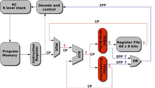
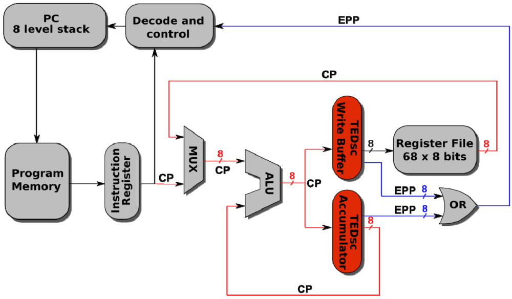
Figure 5 shows the block diagram of the core. The paths that can generate timing errors are highlighted in red. The core contains a total of 20 EDS circuits; 8 of them are in the accumulator register, 8 of them in the register file write buffer, and 4 of them are used for the arithmetic and logic unit (ALU) flags. The error signal paths are highlighted in blue.
The design requires more circuit modifications than a conventional design. For example, we inserted buffers on the fastest paths during the place and route stage to ensure that the hold time requirement for the TED error detection window was met. During the "Decode" stage, there are significant modifications to allow for error recovery.
Figure 5.
TEDsc-enabled subthreshold microprocessor architecture. The timing error signal propagation paths (EPP) are highlighted in blue and the critical paths (CP) in red.
Figure 5.
TEDsc-enabled subthreshold microprocessor architecture. The timing error signal propagation paths (EPP) are highlighted in blue and the critical paths (CP) in red.
3.2. Timing-Error Detection and Recovery
Both the architecture of the core and the timing constraints set during the synthesis ensure that timing errors can only occur during the “Execution” stage. A timing error occurs when a data signal on a critical path arrives too late to the subsequent EDS data storage element (i.e., the latch). At this point, incorrect values can be written to the accumulator and register file. In addition, the Program Counter (PC) and the stack might be incorrectly updated due to incorrect ALU flags.
After a timing error, the core needs to be able to restore the previous state using the following methods. First, when a timing error is detected, the system operation is halted by disabling the clocking. Next, the data stored during the previous cycle is restored (i.e., the previous values of the PC, the accumulator, and the last stack push/pop are stored in the data FFs). Thus, the system stage becomes the previous stage. Finally, the failed instruction is re-executed using two clock cycles instead of one to guarantee an error-free operation. After the two clock cycle execution, the normal operation frequency is restored.
The error signals are not distinguished from each other, but are, instead, combined with one another. Thus, the system does not know which path generated an error. This arrangement is simple and it enables fast operation. With regards to functionality, it is not necessary to know on which path an error occurred.
Correct TED operation requires that signals do not arrive too early or late with respect to a TED window (TEDwin,N), since these signals are not accounted for in real time at the system level or within the EDS. A signal that arrives too early has an insufficient delay time and, thus, it incorrectly arrives in the previous TED detection window (TEDwin,N−1). In other words, a timing error is incorrectly generated (false positive). False positives are avoided by constructing correctly sized delay buffers. When a signal arrives too late (i.e., at TEDwin,N+1), it means that the delay is too large and that an error has not been correctly detected. To avoid these false negatives, timing constraints within the design are implemented to ensure that a signal cannot be delayed too greatly.
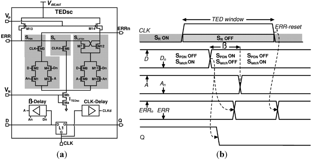
3.3. TEDsc
TEDsc is an EDS circuit [
Figure 6 (a)] that uses subthreshold source-coupled logic (STSCL) to detect timing errors [
15]. Depending on the logic depth, the leakage current, the activity factor, and the operation frequency of a system, STSCL can have several advantages over static CMOS (e.g., tunability, reduced power consumption, and a decreased sensitivity to supply noise [
16,
17]). STSCL has been shown to be advantageous for ultra-low-power (ULP) systems.
Figure 6.
(
a)
TEDsc circuit [
15]; (
b)
TEDsc timing.
Figure 6.
(
a)
TEDsc circuit [
15]; (
b)
TEDsc timing.
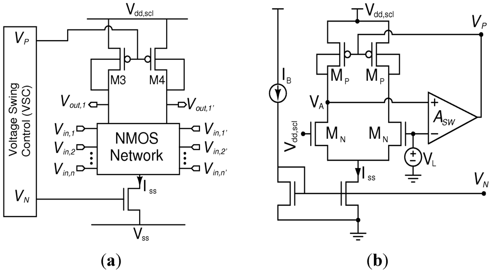
An STSCL gate is composed of a network of differential NMOS pairs, an adjustable PMOS load (M
3,M
4) with output resistance
RP, and an adjustable tail current
ISS [
Figure 7(a)]. The NMOS pairs are used to construct logic gates. The voltage swing is defined as
VSW =
RP·
ISS, and it is maintained by dynamically adjusting the size of
RP and the magnitude of
ISS. Since
ISS can be reduced to the pA range,
RP needs to be in the GΩ range to achieve a proper
VSW (
i.e.,
VSW > 150 mV). By connecting the bulk of the PMOS load devices to the drain, a large
RP is achieved without excessively large transistor lengths [
16,
17].
The size of
RP and the magnitude of
ISS are both adjusted by the voltage swing control (VSC) block as shown in
Figure 7(b). The VSC decreases the dependence on global variations (e.g., supply noise, temperature fluctuations, and ageing). The VSC ensures a voltage swing greater than 150 mV across all global variations. The VSC for
TEDsc uses a two-stage, miller-compensated opamp for ASW. The opamp is able to maintain an open loop gain of 40 dB for all the global process corners. The bias voltage (
VP) from one VSC can be used for a large number of
TEDsc gates [
16].
Figure 7.
(a) Subthreshold source-coupled logic (STSCL) circuit; (b) Voltage swing control (VSC).
Figure 7.
(a) Subthreshold source-coupled logic (STSCL) circuit; (b) Voltage swing control (VSC).
Since
TEDsc uses STSCL, it has the unique ability to adjust its D-to-timing error delay (D-ERRf delay); this results in an adjustable TED window. This ability to adjust the D-ERRf delay can be explained by first understanding that during a D transition,
TEDsc requires a minimum amount of charge (
Qemin) to move from the dynamic output node in order to induce a differential timing error [
15]. Reaching
Qemin is dependent on
ITEDsc and the β-delay that is extended under the CLK high (
i.e.,
tβCLK). For example, when
ITEDsc is increased, the TED window is widened at both of the CLK’s edges since the required
tβCLK is decreased to meet
Qemin.
The starting point of the TED window (
ta2 +
tedge2 from
Figure 4) has two important implications. First, at the positive CLK edge, an excessively early starting point of the TED window (
i.e., (
ta2 +
tedge2)/T
CLK is too large) does not allow for the maximum clock frequency to be reached and, thus, the energy consumption is increased. Second, for a flip-flop based pipeline, an overly delayed TED window starting point (
i.e., due to a low
ITEDsc) does not correctly report all setup time failures as timing errors, which results in a non-functional design. In the presence of large global variation susceptibility, as found in subthreshold, the tunable TED window enables fine tuning on the system level.
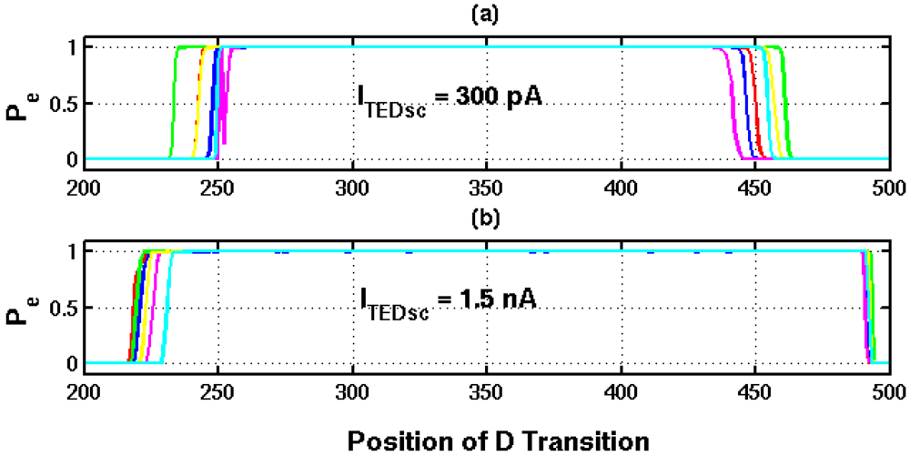
Fine tuning of the TED window is achieved by adjusting
ITEDsc within
TEDsc. To understand how the
ITEDsc affects the TED window, three
TEDsc circuits were measured on the same die.
TEDsc and VSC used the following settings:
Vdd,scl = 400 mV,
VL = 200 mV, and
Vdd = 300 mV. A total of 500 positions of D were applied as input to
TEDsc. There were 16,384 transitions of D at each of the 500 positions. The duty cycle of the CLK was at 50%. The TED window for
TEDsc in
Figure 8 is located between (Position of D Transition) 250 and 500.
Figure 8 shows the error probability of the three
TEDsc circuits as a function of the D transition. For this measurement, the frequency of the CLK was 10.37 kHz.
As shown in
Figure 8, by adjusting
ITEDsc,
TEDsc can adjust its D-ERRf delay. This subsequently makes fine tuning of the TED window (and the uncertainty region) possible. For example, to reduce the D-ERRf delay,
ITEDsc was increased from 300 pA to 1.56 nA (
Figure 8). In previous designs [
14,
15], the uncertainty region and TED window have been fully defined at design time, which is not favorable for weak inversion TED design. Simulations showed an uncertainty region (
i.e., A
2, A
4) of approximately the same size as found in measurement [
15].
Figure 8.
(a) ITEDsc at 300 pA; (b) When ITEDsc is increased to 1.5 nA, the size of the TED window increases.
Figure 8.
(a) ITEDsc at 300 pA; (b) When ITEDsc is increased to 1.5 nA, the size of the TED window increases.
As the microprocessor’s performance is altered by local and global variations, it is essential that the EDS circuit operate correctly and accurately. Through simulations,
TEDsc was shown to be robust to both local and global variations. Local variations were accounted for by applying Monte-Carlo simulations at each process corner (
i.e., TT, FF, SS, SF, and FS). This simulation also showed a robustness to global process corners due to the VSC. Additionally,
TEDsc showed a correct functionality from −40 °C to 90 °C as a result of the VSC. Using STSCL also reduces the sensitivity of
TEDsc to changes in the supply voltage [
17]. In addition, the probability of a fast change in the supply voltage at the exact same time that D transitions is low. To verify this, we applied a sawtooth-wave ripple voltage from 0 to 40 mV and a frequency from 10 MHz to 100 MHz to
TEDsc; the correct functionality was shown under these ripple conditions.
The effects of local variations on
TEDsc are minimized by proper sizing techniques developed by Wang, Calhoun and Chandrakasan [
3] and Alioto and Leblebici [
18]. The effects of global variations on
TEDsc are minimized due the STSCL design choice. As mentioned in
Section 3.3, STSCL uses the VSC to maintain proper operation during the application of both static and dynamic global variations [
17]. As mentioned in
Section 2.2, larger local variations increase the size of
ta2 and
tedge2. This fundamentally limits the speed of the entire TED system since if (
ta2 +
tedge2)/
TCLK is too large, there is not ample time to detect errors.
3.4. Implementation of Core 1 and 2
To compare the benefits of TED, we designed a TED-enabled core (Core 1) and a non-TED core (Core 2). The designs of both cores were fabricated in 65 nm CMOS. The supply voltage range of both designs is from 300 mV to 500 mV, which is at the edge or below the strong inversion region for the process and all the digital cells. However, we optimized TEDsc to work deep into subthreshold; the analysis below will only include 300 mV and 400 mV operation points.
To simplify the design process of Core 1, two power domains were used in the design. The instruction memory and the error propagation path are located within one power domain, while the rest of the design is in a second power domain. The size of the instruction memory is 256 instructions and the size of the register file is 68 bytes. The area of the TED core (without instruction memory) is approximately 50,000 μm2. The length of the CLK period is approximately 160 times the FO4 delay. The clock period is limited by the “Execute” stage and EDS design.
The foundries did not provide digital EDA tool library information for subthreshold operation. To acquire the library’s timing and power information for the EDA tools, we re-characterized the standard cells for subthreshold operation by using the Synopsys library characterization workflow. During the re-characterization process, we used the standard libraries as templates, considered all the timing arcs, and acquired the new timing and power information via analog simulation. The re-characterization process was repeated for the typical, best, and worst corners. The acquired library information was used by the EDA tools in the automated design flow. Due to their sensitivity variation in subthreshold, the smallest gates were removed from the libraries.
It was not possible to characterize the EDS element and include it to the digital library due to the asynchronous nature of the element’s error signal. Furthermore, the VSC block that generates bias voltages for the TEDsc blocks is inherently analog. Therefore, a digital simulation of the full system was not possible. An analog simulation of the system would have been excessively long. Thus, we performed a mixed-mode simulation on the system. The VCS and TEDsc blocks were simulated using Spice transistor level models. All of the digital blocks were simulated using the post-layout netlist (including parasitics). Mentor Graphics Questa ADMS was used to perform the mix-mode simulation.
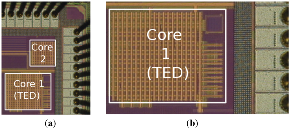
The die microphotograph of Core 1 (TED) and Core 2 without instruction memory is shown in
Figure 9. Both Cores include all the logic, delays, and buffers. The VSC block and the EDS circuits are also shown in Core 1 (TED).
Figure 9.
(a) The microcontroller core with and without TED are shown as Core 1 (TED) and 2, respectively; (b) Core 1 (TED) including the VSC and TEDsc circuits.
Figure 9.
(a) The microcontroller core with and without TED are shown as Core 1 (TED) and 2, respectively; (b) Core 1 (TED) including the VSC and TEDsc circuits.
Table 1 shows a comparison of Core 1 and Core 2. The area of Core 2 is approximately 18,000 µm
2, which is approximately 64% smaller than that of the TED version. For the comparison, the chip I/O compatibility level-shifters present in the subthreshold version are excluded, which gives the total area for the TED version as approximately 50,000 µm
2. The VSC block occupies an area of approximately 1750 µm
2 in the subthreshold design. It should be noted that in a larger design, the VSC area gets proportionally smaller. The areas of the different blocks were measured so that only the active area occupied by the blocks was taken into account.
The data in
Table 1 shows that both the clock delay cells and the buffer cells occupy a substantially larger area than in the nominal voltage design. The number and the area of the logic ports are comparable. The area of the data storage elements is approximately two times larger in the subthreshold design, which can be explained by the fact that the EDS cells in general are larger in area than their conventional style counterparts. This applies especially to the EDS circuits designed for subthreshold operation due to their variation immunity requirements as explained in
Section 3.3. The area in the table that is unaccounted for is occupied by the decap and antenna protection elements, and in Core 1 by the VSC block. It should be noted that the Core 1 (TED) design has not been optimized area-wise. Also, the I/O port functionality has been excluded from the Core 1 design. This makes the comparison somewhat less favorable for the Core 1 design in terms of the area. Also, the error recovery mechanism modification adds to the logic size slightly. The last columns of the table show the percentage of the area of the Core 1 design compared to the area of the nominal voltage design (Core 2).
Table 1.
An area comparison of Core 1 (TED) and Core 2.
Table 1.
An area comparison of Core 1 (TED) and Core 2.
| | Core 2 (Total Area ≈ 18,000 µm2) | Core 1 (TED) (Total Area ≈ 50,000 µm2) | Area of Cells in Core 1 ÷ Area of Cells in Core 2 (
i.e., % larger area that Core 1 uses than Core 2) |
|---|
| Number of Cells | % of the Total Area | Number of Cells | % of the Total Area |
|---|
| Buffer Cells | 139 | 2.5% | 934 | 5% | 538% |
| Clock Buffer Cells | 223 | 3.5% | 66 | <1% | 45% |
| Clock Delay Cells | 37 | 1% | 1580 | 21% | 4644% |
| Data Storage Cells | 777 | 35% | 897 | 27% | 205% |
| Logic Port Cells | 1942 | 45% | 2191 | 17% | 108% |
| Filler Cells | 563 | 10% | 4756 | 19% | 539% |


