Article

Exploration of Sub-VT and Near-VT 2T Gain-Cell Memories for Ultra-Low Power Applications under Technology Scaling

1
Institute of Electrical Engineering, Ecole Polytechnique Fédérale de Lausanne, Station 11, Lausanne,VD 1015, Switzerland
2
VLSI Systems Center, Ben-Gurion University of the Negev, POB 653, Be'er Sheva 84105, Israel
3
Faculty of Engineering, Bar-Ilan University, Ramat-Gan 52900, Israel
*
Author to whom correspondence should be addressed.
J. Low Power Electron. Appl. 2013, 3(2), 54-72; https://doi.org/10.3390/jlpea3020054
Submission received: 4 February 2013 / Revised: 16 March 2013 / Accepted: 19 March 2013 / Published: 29 April 2013
(This article belongs to the Special Issue Selected Papers from SubVt 2012 Conference)

Abstract

:
Ultra-low power applications often require several kb of embedded memory and are typically operated at the lowest possible operating voltage ( V DD ) to minimize both dynamic and static power consumption. Embedded memories can easily dominate the overall silicon area of these systems, and their leakage currents often dominate the total power consumption. Gain-cell based embedded DRAM arrays provide a high-density, low-leakage alternative to SRAM for such systems; however, they are typically designed for operation at nominal or only slightly scaled supply voltages. This paper presents a gain-cell array which, for the first time, targets aggressively scaled supply voltages, down into the subthreshold (sub- V T ) domain. Minimum V DD design of gain-cell arrays is evaluated in light of technology scaling, considering both a mature 0.18 µm CMOS node, as well as a scaled 40 nm node. We first analyze the trade-offs that characterize the bitcell design in both nodes, arriving at a best-practice design methodology for both mature and scaled technologies. Following this analysis, we propose full gain-cell arrays for each of the nodes, operated at a minimum V DD . We find that an 0.18 µm gain-cell array can be robustly operated at a sub- V T supply voltage of 400 mV, providing read/write availability over 99% of the time, despite refresh cycles. This is demonstrated on a 2 kb array, operated at 1 MHz, exhibiting full functionality under parametric variations. As opposed to sub- V T operation at the mature node, we find that the scaled 40 nm node requires a near-threshold 600 mV supply to achieve at least 97% read/write availability due to higher leakage currents that limit the bitcell’s retention time. Monte Carlo simulations show that a 600 mV 2 kb 40 nm gain-cell array is fully functional at frequencies higher than 50 MHz.

1. Introduction

Many ultra-low power (ULP) systems, such as biomedical sensor nodes and implants, are expected to run on a single cubic-millimeter battery charge for days or even for years, and therefore are required to operate with extremely low power budgets. Aggressive supply voltage scaling, leading to near-threshold (near- V T ) or even to subthreshold (sub- V T ) circuit operation, is widely used in this context to lower both active energy dissipation and leakage power consumption, albeit at the price of severely degraded on/off current ratios ( I on / I off ) and increased sensitivity to process variations [1]. The majority of these biomedical systems require a considerable amount of embedded memory for data and instruction storage, often amounting to a dominant share of the overall silicon area and power. Typical storage capacity requirements range from several kb for low-complexity systems [2] to several tens of kb for more sophisticated systems [3]. Over the last decade, robust, low-leakage, low-power sub- V T memories have been heavily researched [4,5,6]. In order to guarantee reliable operation in the sub- V T domain, many new SRAM bitcells consisting of 8 [7,8], 9 [5,9], 10 [4], and up to 14 [2] transistors have been proposed. These bitcells utilize the additional devices to solve the predominant problems of write contention and bit-flips during read, and, in addition, some of the designs reduce leakage by using transistor stacks. All these state-of-the-art sub- V T memories are based on static bitcells, while the advantages and drawbacks of dynamic bitcells for operation in the sub- V T regime have not yet been studied.
Conventional 1-transistor-1-capacitor (1T-1C) embedded DRAM (eDRAM) is incompatible with standard digital CMOS technologies due to the need for high-density stacked or trench capacitors. Therefore, it cannot easily be integrated into a ULP system-on-chip (SoC) at low cost. Moreover, low-voltage operation is inhibited by the offset voltage of the required sense amplifier, unless special offset cancellation techniques are used [10].
Gain-cells are a promising alternative to SRAM and to conventional 1T-1C eDRAM, as they are both smaller than any SRAM bitcell, as well as fully logic-compatible. Much of the previous work on gain-cell eDRAMs focuses on high-speed operation, in order to use gain-cells as a dense alternative to SRAM in on-chip processor caches [11,12], while only a few publications deal with the design of low-power near- V T gain-cell arrays [13,14,15]. A more detailed review of previous work in the field of gain-cell memories, including target application domains and circuit techniques, can be found in [16]. The possibility of operating gain-cell arrays in the sub- V T regime for high-density, low-leakage, and voltage-compatible data storage in ULP sub- V T systems has not been exploited yet. One of the main objections to sub- V T gain-cells is the degraded I on / I off current ratio, leading to rather short data retention times compared with the achievable data access times. However, the present study shows that these current ratios are still high enough in the sub- V T regime to achieve short access and refresh cycles and high memory availability, at least down to 0.18 µm CMOS nodes. While gain-cells are considerably smaller than robust sub- V T SRAM bitcells, they also exhibit lower leakage currents, especially in mature CMOS nodes where sub- V T conduction is the dominant leakage mechanism. Recent studies for above- V T , high-speed caches show that gain-cell arrays can even have lower retention power (leakage power plus refresh power) than SRAM (leakage power only) [17]. However, a direct power comparison between gain-cell eDRAM and SRAM is difficult and not within the scope of this paper; for example, an ultra-low power sub- V T SRAM implementation [2] employs power gating of all peripheral circuits and of the read-buffer in the bitcell, while most power reports for gain-cell eDRAMs include the overhead of peripherals. Compared with SRAM, gain-cells are naturally suitable for two-port memory implementation, which provides an advantage in terms of memory bandwidth, and enables simultaneous and independent optimization of write and read reliability. Finally, while local parametric variations directly compromise the reliability of the SRAM bitcell (write contention, and data loss during read), such parametric variations only impact the access and retention times of gain-cells, which is not a severe issue when targeting the typically low speed requirements of ULP applications, such as sub- V T sensor nodes or biomedical implants.
To start with, we consider sub- V T gain-cell eDRAM design in a mature 0.18 µm CMOS node, which is typically used to: (1) easily fulfill the high reliability requirements of ULP systems; (2) reach the highest energy-efficiency of such ULP systems, typically requiring low frequencies and duty cycles [18]; and (3) achieve low manufacturing costs. In a second step, we investigate the feasibility of sub- V T gain-cell eDRAMs under the aspect of technology scaling. In particular, in addition to the mature 0.18 µm CMOS node, we analyze low voltage gain-cell operation in a 40 nm CMOS technology node. We show that deep-nanoscale gain-cell arrays are still feasible, despite the reduced retention times inherent to these nodes. Due to high refresh rates, we identify that the minimum supply voltage ( V DDmin ) that ensures an array availability of 97% is in the near- V T domain.

1.1. Contributions:

The contributions of this work can be summarized as follows:
  • We investigate the minimum achievable supply voltage for ultra-low power gain-cell operation.
  • We analyze gain-cell arrays from a technology scaling perspective, examining the design trade-offs that arise due to the inherent characteristics of various technology nodes.
  • For the first time, we present a fully functional gain-cell array at a deeply scaled technology node, as low as 40 nm.
  • For the first time, we present a gain-cell array operated in the sub- V T domain.

1.2. Outline:

The remainder of this article is organized as follows. Section 2 explains the best-practice 2T gain-cell design in light of technology scaling, emphasizing the optimum choices of the write access transistor, read access transistor, storage node capacitance, and word line underdrive voltage for different nodes. Section 3 and Section 4 present detailed implementation results of a 2 kb gain-cell memory in a 0.18 µm and in a 40 nm CMOS node, respectively. Section 5 summarizes the findings of this article.

2. Two-Transistor (2T) Sub- V T Gain-Cell Design

Previously reported gain-cell cell topologies include either two or three transistors and an optional MOSCAP or diode [16]. While the basic two-transistor (2T) bitcell has the smallest area cost, it limits the number of cells that can connect to the same read bitline (RBL) due to leakage currents from unselected cells masking the sense current [19]. However, as many ULP systems require only small memory arrays with relatively few cells per RBL, in the following section, we consider the implementation of a 2T bitcell as a viable low-voltage option and propose a best-practice 2T bitcell design for the considered technology nodes (0.18 µm and 40 nm).

2.1. 2T Gain-Cell Implementation Alternatives

Figure 1 shows the four basic options for implementing a 2T gain-cell, allowing both the write transistor (MW) and the combined storage and read transistor (MR) to be implemented with either an NMOS or a PMOS device. These standard topologies require the following control schemes to achieve robust write and read operations. A boosted write wordline (WWL) voltage is required during write access due to V T drop across MW; above V DD for the NMOS option ( V BOOST ) and below V SS for the PMOS option ( V NWL ). For a read operation with a PMOS MR, the parasitic RBL capacitance is pre-discharged, and the read wordline (RWL) is subsequently raised. If the selected bitcell’s storage node (SN) holds a “0”, MR is conducting and charges RBL past a detectable sensing threshold. If SN holds a “1”, MR is cut off, such that RBL remains discharged below the sensing threshold. Using an NMOS transistor to implement MR provides the exact opposite operation, i.e., RBL is pre-charged and RWL is lowered to initiate a read.
In the considered 0.18 µm CMOS technology, both MW and MR can be implemented with either standard- V T core or high- V T I/O devices. In more advanced technology nodes, typically starting with the 130 nm or 90 nm node for most semiconductor foundries, several V T options become available for core devices, most commonly low- V T (LVT), standard- V T (SVT), and high- V T (HVT) devices. One of the primary considerations for gain-cell implementation is achieving high retention time, i.e., the time it takes for the level stored on SN to deteriorate through leakage currents. In mature, above-100 nm CMOS nodes, subthreshold conduction is the dominant leakage mechanism, compromising data retention in any 2T gain-cell through the channel of MW, as shown in Figure 2(a). Therefore, the primary selection criterion for the device type of MW is to minimize subthreshold conduction. Note that subthreshold conduction of MW weakens both a logic “1” and a logic “0” level, whenever the write bitline (WBL) voltage is opposite to the SN voltage.
Figure 1. 2T gain-cell implementation options including the schematic waveforms.
Jlpea 03 00054 g001
Figure 2. Leakage components that are considered for the choice of the best-practice write and read transistor implementations, for (a) Mature CMOS nodes; and (b) Scaled CMOS nodes.
Jlpea 03 00054 g002
In more advanced, sub-100 nm CMOS nodes, there are other significant leakage mechanisms that can compromise data integrity. (Note that in the sub- V T region, these mechanisms are still negligible, as compared with subthreshold conduction. However, as shown in Section 2.3.2, at near- V T supplies, some of the mechanisms must be considered). Only leakage components that bring charge onto the SN or take charge away from SN need to be considered in terms of retention time, while other leakage components are merely undesirable in terms of static power consumption. Figure 2(b) schematically shows the main leakage components that can compromise the stored level in sub-100 nm nodes, including reverse-biased pn-junction leakage ( I diff ), gate-induced drain leakage ( I GIDL ), gate tunneling leakage ( I gate ), edge-direct tunneling current ( I EDT ), and subthreshold conduction ( I sub ). When employing a PMOS MW, the bulk-to-drain leakages ( I diff and I GIDL ) weaken a logic “0” and strengthen a logic “1”, but have the opposite impact (strengthen a logic “0” and weaken a logic “1”) when MW is implemented with an NMOS device. During standby, MW is always off and has no channel; therefore, forward gate tunneling ( I gate ) from the gate into the channel region and into the two diffusion areas that would occur in a turned-on MOS device is of no concern here. Only the edge-direct tunneling current, from the diffusion connected to the SN in the absence of a strongly inverted channel, compromises data integrity. When using an NMOS MW, edge-direct tunneling discharges a logic “1”, while it charges a logic “0” for a PMOS MW.
The only leakage through MR that affects the stored data level is gate tunneling. During standby, there is no channel formation in MR, no matter what the stored data level is. For example, if using an NMOS MR, both RWL and RBL are charged to V DD during standby, such that even a logic “1” level results in zero gate overdrive. In this case, both diffusion areas of MR are at the same potential as the SN, eliminating tunneling currents between the diffusions and the gate ( I EDT = 0 ). However, tunneling might occur from the gate directly into the grounded bulk ( I gate ), weakening a logic “1”. If the same cell stores a logic “0”, tunneling between the gate and bulk is avoided ( I gate = 0 ), while reverse tunneling from the diffusions ( I EDT ) into the gate can charge the logic “0” level. The exact opposite biasing conditions and corresponding tunneling mechanisms are found when implementing MR with a PMOS.

2.2. Best-Practice Write Transistor Implementation

2.2.1. Mature 0.18 µm CMOS Node

For the ULP sub- V T applications, long retention times that minimize the number of power-consuming refresh cycles are of much higher importance than fast write access. Therefore, low subthreshold conduction becomes the primary factor in the choice of a best practice write transistor in the 0.18 µm node. The subthreshold conduction of NMOS and PMOS, core and I/O devices offered in this process are shown in Figure 3(a). Clearly, the I/O PMOS device has the lowest subthreshold conduction I sub ( V GS = 0 V , V DS = V DD ) among all device options and across all standard process corners, leading to the longest retention time. At a 400 mV sub- V T V DD , the on-current I on ( V GS = V DD , V DS = V DD ) of this preferred I/O PMOS device is still four orders of magnitude larger than I sub , as shown in Figure 3(b), which results in sufficiently fast write and refresh operations compared with the achievable retention time. This holds for temperatures up to 37 C, which is considered a maximum, worst-case temperature for ULP systems that are often targeted at biomedical applications, typically attached to the human body, and hardly suffer from self-heating due to low computational complexity. Nevertheless, for temperatures as high as 125 C, a sufficiently high I on / I sub ratio of four orders of magnitude is still achieved at a slightly higher supply voltage of 500 mV.
Figure 4(a) shows the worst-case time dependent data deterioration after writing into a 2T gain-cell with a PMOS I/O write transistor under global and local variations. The blue (bottom) curves show the deterioration of a logic “0” level with WBL tied to V DD , and the red (top) curves show the deterioration of a logic “1” level with WBL tied to ground. The plot was simulated with a sub- V T 400 mV V DD assuming a storage node capacitance of 2.5 fF. A worst-case retention time of 40 ms can be estimated from this figure, corresponding to the minimum time at which the “0” and “1” levels intersect. It is clear that a logic “0” level decays much faster than a logic “1” level, corresponding with previous reports for the above- V T domain [11,13]. In fact, the decay of a “1” level is self-limited due to the steady increase of the reverse gate overdrive ( V GS , MW = V DD V SN ) and the increasing body effect ( V BS , MW = V DD V SN ) of MW with progressing decay. Both of these effects suppress the device’s leakage. Furthermore, the charge injection (CI) and clock feedthrough (CF) that occur at the end of a write access (when MW is turned off) cause the SN voltage level to rise, strengthening a “1” and weakening a “0” level [16,20]. Therefore, careful consideration must be given to the initial state of the “0” level following a write access, as will be discussed in Section 2.4.
Figure 3. (a) Subthreshold conduction of different transistor types in an 0.18 µm node; and (b) I/O PMOS I on / I sub current ratio as a function of V DD for the typical-typical (TT) process corner at different temperatures.
Jlpea 03 00054 g003
Figure 4. (a) Worst-case retention time estimation of 0.18 µm sub- V T gain-cell with V DD = 400 mV ; (b) Best-practice gain-cell for sub- V T operation in 0.18 µm CMOS.px
Jlpea 03 00054 g004

2.2.2. Scaled 40 nm CMOS Node

While choosing the best device option for MW, subthreshold conduction must again be kept as small as possible, as it affects both a “1” and a “0” level. The diffusion leakage, the GIDL current, and the edge-direct tunneling current weaken one logic level, while they strengthen the other. However, all three leakage components work against the logic level that has already been weakened through CI and CF at the end of a write pulse. For example, with a PMOS MW, the logic “0” level is weakened through a positive SN voltage step when closing MW, while I GIDL , I diff , and I EDT further pull up SN, deteriorating the stored “0”. Therefore, in order to protect the already weaker level, the optimum device selection aims at minimizing all of these leakage components. Figure 5(a) shows the leakage components of minimum sized devices provided in the 40 nm process (the LVT devices were left out of the figure for display purposes, as their leakage is significantly higher than the leakage of other devices) at a near- V T supply voltage of 600 mV. This figure clearly shows that despite the increasing significance of other leakage currents with technology scaling, I sub is still dominant at this node (some of the leakage components are not modeled for the I/O devices; however, this does not impact our analysis, as the PMOS HVT already provides the lowest total leakage). However, the advantage of using an I/O device is lost, and a more compact HVT PMOS device provides the lowest total leakage. This trend is confirmed when evaluating the leakage components of intermediate process nodes, as well, showing that the leakage benefits of using an I/O device deteriorate to the point where the area versus leakage trade-off favors the use of an HVT device at around the 65 nm node.
Figure 5. (a) Leakage components of various devices in the considered 40 nm node at a near- V T supply voltage of 600 mV; (b) Worst-case I on ( weak 1 ) / I off ( weak 0 ) of MR, implemented with LVT, SVT, and HVT devices. Both plots were simulated under typical conditions.
Jlpea 03 00054 g005

2.3. Best-Practice Read Transistor Implementation

2.3.1. Mature 0.18 µm CMOS Node

At the onset of a read operation, capacitive coupling from RWL to SN causes a voltage step on SN [20]. Our analysis from the previous section showed that MW should be implemented with a PMOS device, resulting in a strong logic “1” and a weaker logic “0”. Therefore, it is preferable to implement MR with an NMOS transistor that employs a negative RWL transition for read assertion. The resulting temporary decrease in voltage on SN counteracts the previous effects of CI and CF, thus improving the “0” state during a read operation (effect is reversed upon deassertion of the RWL). As a side effect, this negative SN voltage step also lowers the “1” level and therefore slightly slows down the read operation; however, this level is already initially boosted due to deassertion of the WWL. An additional and perhaps more significant reason to choose an NMOS device for readout is that NMOS devices are approximately an order-of-magnitude stronger than their PMOS counterparts at sub- V T voltages. Therefore, implementing MR with an NMOS device provides a fast read access, which not only results in better performance but also is essential for ensuring high array availability. As mentioned, the considered 0.18 µm process provides only core and I/O devices, and considering the three-orders-of-magnitude higher on-current for core devices at sub- V T , the choice of an NMOS core MR is straightforward.
To summarize, the most appropriate 2T gain-cell for sub- V T operation in an above-100 nm CMOS node comprises an I/O PMOS write transistor and a core NMOS read transistor, as illustrated in Figure 4(b). The resulting hybrid NMOS/PMOS gain-cell shares the n-well on three sides between neighboring cells [19] to keep the area cost low, as discussed in Section 3.

2.3.2. Scaled 40 nm CMOS Node

When considering the best device type for scaled nodes, the large number of options presents some interesting trade-offs for the implementation of MR. The increasing gate leakage currents ( I gate and I EDT ) at scaled nodes could potentially present an advantage for a thick oxide I/O device due to its reduced gate tunneling. However, at low voltages, the tunneling currents are small in comparison with the subthreshold conduction through MW, as shown in Figure 5(a). In addition, I gate and I EDT actually appear in opposite directions, as the stored “0” level rises, further reducing their impact. On the other hand, the two primary considerations for the above-100 nm nodes are even more relevant at scaled nodes. The achievable retention time in the 40 nm process turns out to be approximately three orders-of-magnitude lower than that of the 0.18 µm node. Therefore, the negative step caused by RWL coupling to SN is even more important, and fast reads are essential to provide sufficient array availability, despite the high refresh rates. To further enhance the read step, layout techniques can be implemented to increase the capacitive coupling between RWL and SN. However, when considering read access times, additional trade-offs arise. For maximum read performance, MR could be implemented with an LVT device. At the 40 nm node, an LVT NMOS provides an 8× increase in on-current at 400 mV compared with an SVT NMOS. However, as the supply voltage is increased, this benefit reduces to 3× at 600 mV. The superior on-currents of LVT devices, as compared with SVT or HVT options, come at the expense of much higher off-currents, as well as increased process variations. When choosing the read device, this trade-off must be taken into consideration, as it is mandatory to correctly differentiate between the discharged level of RBL due to a stored “1” and the depleted level due to a weak stored “0”. Furthermore, the unselected cells on the same column of a selected cell storing a “1” will start to counteract the discharge of RBL during a read, as V GS , MR unselected = V DD V RBL . In effect, this limits the speed and minimum discharge level of RBL, according to the drive strength of the unselected MR devices. When considering sub- V T operation in the 40 nm node, the relatively low subthreshold conduction of the SVT, HVT, and I/O devices renders the LVT the only feasible option for MR to achieve a reasonable RBL discharge time. However, as V DD is increased into the near- V T region, an SVT device provides sufficient on-current, while the higher V T and lower leakage enable better reliability under process variations, as well as improved array availability.
Figure 5(b) shows the worst case current ratio I on / I off of the NMOS read transistor MR, implemented with different device types as a function of V DD . I on is given for a weak “1” level, estimated as the steady state high voltage of SN when tying WBL to V DD ( V SN = 0 . 85 V DD ). I off is given for a weak “0” level, estimated at V SN = 0 . 4 V DD , which would provide a sufficient margin to differentiate between the two levels (this is verified for the chosen implementation at the minimum feasible bias in Section 4). For supply voltages below 600 mV, the LVT device has the highest current ratio and is therefore preferred, as it provides the best achievable array availability. Likewise, the SVT device is preferred for V DD between 600 and 800 mV, while the HVT device is the best option for even higher V DD .

2.4. Storage Node Capacitance and WWL Underdrive Voltage

2.4.1. Mature 0.18 µm CMOS Node

To close the design of the 2T bitcell, two important design parameters must be taken into consideration. First, the storage node capacitance ( C SN ), primarily made up of the diffusion capacitance of MW and the gate capacitance of MR, is typically around 1 fF for minimum device sizes. However, we find that by applying layout techniques, such as metal stacking, this value can be extended by over 5×, providing a configurable design parameter. Second, to address the V T drop across MW especially affecting the write “0” operation (but also the write “1” operation in the sub- V T regime), an underdrive voltage ( V NWL ) needs to be applied to WWL, the magnitude of which affects the write access time and the SN voltage.
Figure 6(a) shows the storage node voltage ( V SN ) after a write “0” access as a function of C SN and V NWL , before and after closing MW. Figure 6(b) emphasizes the impact of CI and CF by showing the voltage step Δ V that occurs while closing MW. It is clear that any V NWL above −650 mV already results in a degraded logic “0” transfer prior to turning off MW. Δ V can be reduced by increasing C SN and by decreasing the magnitude of V NWL . Therefore, on the one hand, V NWL must be low enough to ensure a proper logic “0” transfer, while, on the other hand, it should be as high as possible to minimize Δ V . The optimum value for V NWL leading to the strongest “0” state after a completed write operation is found to be −650 mV, as shown in Figure 6(a). The optimum value for C SN is clearly the maximum displayed value of 2.5 fF.
Figure 6. Following a write “0” operation: (a) V SN before and after closing MW, as a function of C SN and V NWL ; (b) Δ V due to charge injection from MW and due to capacitive coupling from WWL to SN.
Jlpea 03 00054 g006

2.4.2. Scaled 40 nm CMOS Node

It is clear that the storage node capacitance should always be as big as possible, regardless of the technology node. This not only results in an improved initial “0” level, as shown above, but also provides more stored charge and thus extends the retention time. A general characteristic of scaled CMOS nodes is the increased number of routing layers, which in the case of gain-cell design, can be used to build up the storage node capacitor. Here, we assume that all available metal layers can be used at no additional cost, as the memory is going to be embedded in a system-on-chip that already uses all the metal layers. Moreover, with technology scaling, the aspect ratio of metal wires changes to narrower but higher, and wires can be placed closer to each other, which is beneficial in terms of side-wall parasitic capacitance. However, much of this benefit is offset by the lower dielectric constants of the insulating materials (low-k) integrated into digital processes with technology scaling. In addition, the absolute footprint of the bitcell shrinks with technology, making it more challenging to allocate many inter-digit fingers for a high capacitance. In fact, in the considered 40 nm node, the footprint of a gain-cell containing only two core devices is so small that the minimum width and spacing rules for medium and thick metals are too large to exploit for increasing the capacitance of the SN. Therefore, our layout of the 40 nm cell is limited to 5 routing layers, and the overall SN capacitance is much lower than that achieved in the 0.18 µm node. Figure 7(a) summarizes the achievable storage node capacitance according to the number of thin metal layers provided by the two considered technology nodes.
Figure 7(b) shows the 40 nm SN voltage step Δ V that occurs during the positive edge of WWL for a logic “0” transfer. As already observed for the 0.18 µm node, Δ V decreases with increasing SN capacitance and with decreasing WWL step size (i.e., with decreasing absolute value of the underdrive voltage, V NWL ). While the charge injected from the large channel area of the selected I/O PMOS write transistor in the mature technology node results in a large voltage step severely threatening data integrity, the problem is slightly alleviated in more advanced nodes where small core transistors are preferred. The resulting voltage steps of 10 to 45 mV are rather small compared with the minimum V DD where high array availability is achieved (as will be shown in Section 4). Moreover, it is worth mentioning that strong “0” levels are transferred to SN even with the least aggressive underdrive voltage of 0 . 4 V (however, at the expense of write access time). Therefore, the Δ V values in Figure 7(b) also correspond to the final SN voltage right after the write access. The final choice of V NWL for the 40 nm node needs to account for the write access time, which must remain short to guarantee high array availability in a node with high leakage and short retention time (see Section 4). Therefore, Figure 7(c) shows the final V SN after CI and CF, as a function of the write pulse width. Over a large range of pulse widths as short as several ns, an underdrive voltage of −700 mV results in the strongest “0” levels, and is therefore preferred. Less underdrive, e.g., −500 mV, would result in weak “0” levels for pulse widths that are shorter than 3 ns.
Figure 7. (a) Storage node capacitance versus number of employed metal layers; (b) Δ V due to CI and CF, as a function of C SN and V NWL , for V DD = 700 mV ; (c) V SN after CI and CF versus write pulse width.
Jlpea 03 00054 g007

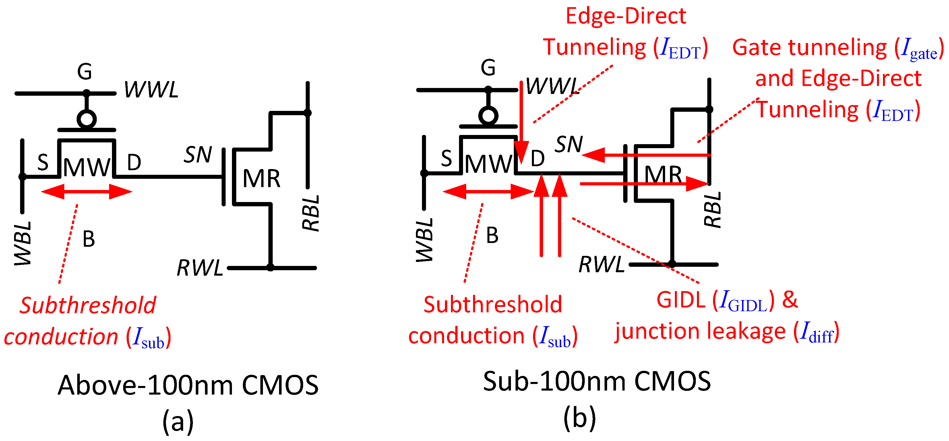
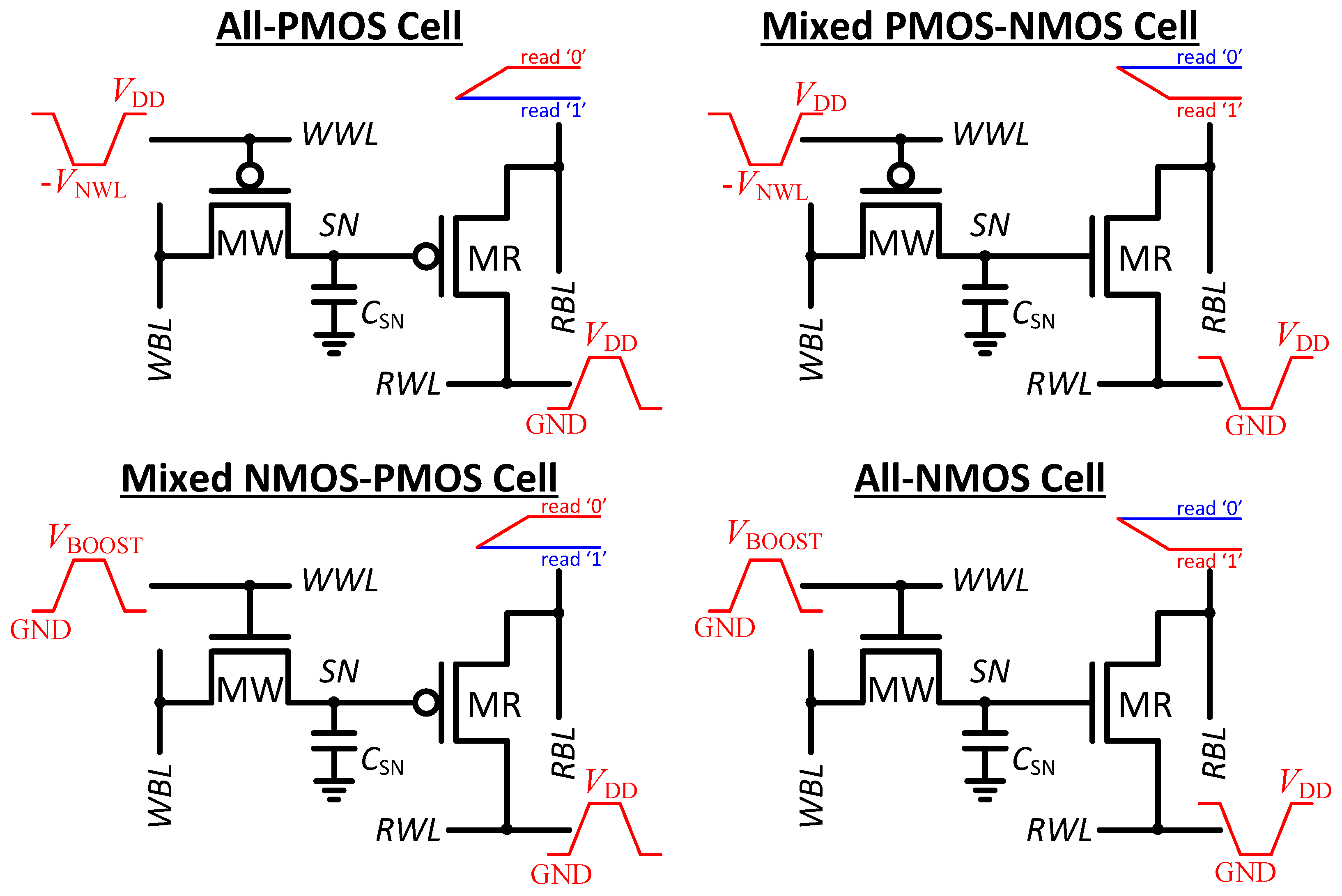
3. Macrocell Implementation in 0.18 µm CMOS

This section presents a 64 × 32 bit (2 kb) memory macro based on the previously elaborated 2T gain-cell configuration (Figure 4(b)), implemented in a bulk CMOS 0.18 µm technology. The considered V DD of 400 mV is clearly in the sub- V T regime, as V T of MW and MR are −720 mV and 430 mV, respectively. Special emphasis is put on the analysis of the reliability of sub- V T operation under parametric variations. While the address decoders and the sense buffers are built from combinational CMOS gates and operate reliably in the sub- V T domain [21], the analysis focuses on the write-ability, data retention, and read-ability of the gain-cell. All simulations assume a 1 µs write and read access time (1 MHz operation); a 3-metal SN capacitance of 2.5 fF, providing a retention time of 40 ms (according to previously presented worst case estimation); a temperature of 37 C and account for global and local parametric variations (1k-point Monte Carlo sampling).
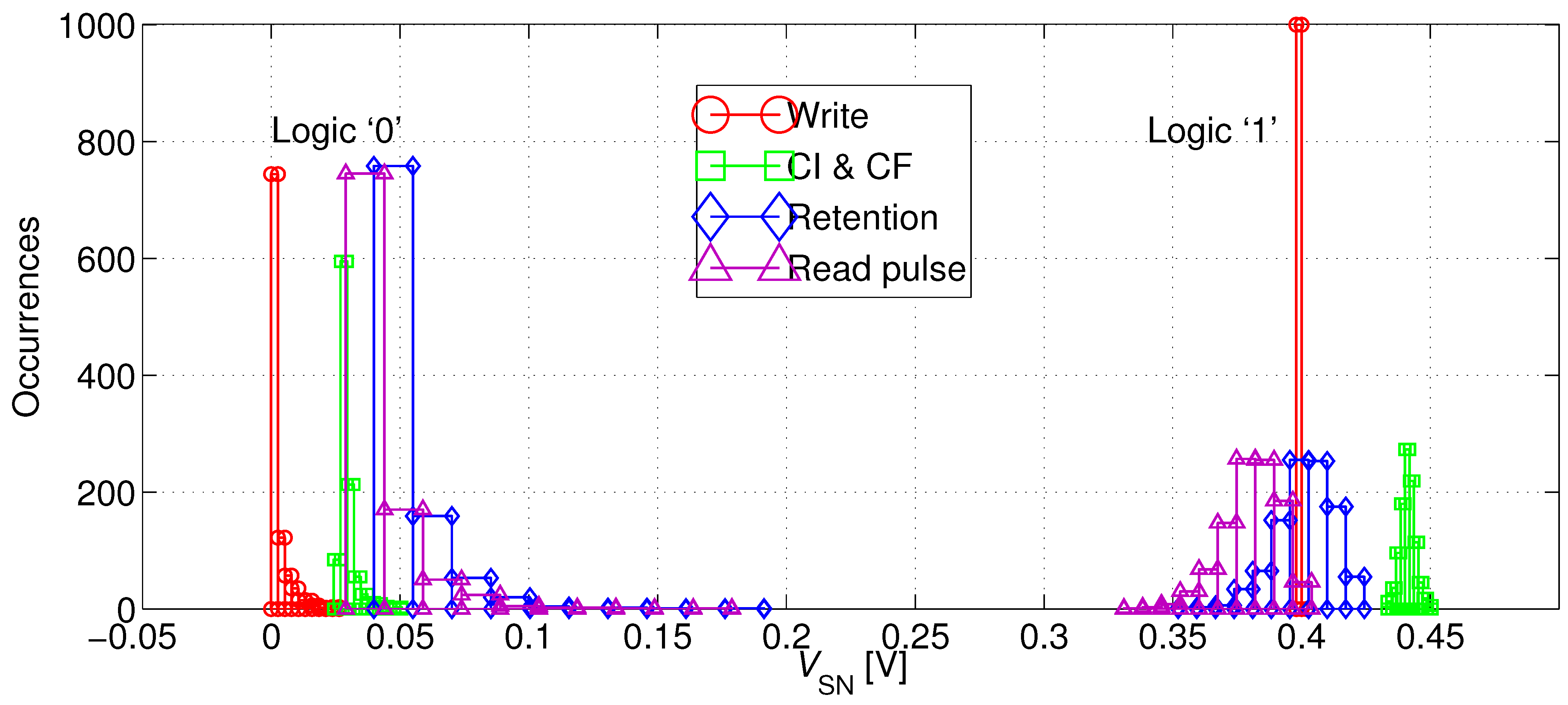
Figure 8 plots the distribution of the bitcell’s SN voltage at critical time points for the “0” and the “1” states. As expected, nominal 0 V and 400 mV levels are passed to SN just before the positive edge of the write pulse. CI and CF cause the internal levels to rise by 20–50 mV, resulting in a slightly degraded “0” level and an enhanced “1” level, while the distributions remain sharp. After a 40 ms retention period with a worst-case opposite WBL voltage, the distributions are spread out, but the “1” levels are still strong, while the extreme cases of the “0” levels have severely depleted, approaching 200 mV. However, the “0” and “1” levels are still well separated, and moreover, the “0” levels are improved following the falling RWL transition, resulting in a 10–20 mV decrease.
Figure 8. Distribution of the SN voltage of a logic “0” and a logic “1” at critical time points: (1) [circles] directly after a 1 µs write access (before turning off MW); (2) [squares] after turning off MW; (3) [diamonds] after a 40 ms retention period under worst-case WBL conditions; and (4) [triangles] during a read operation.
Jlpea 03 00054 g008
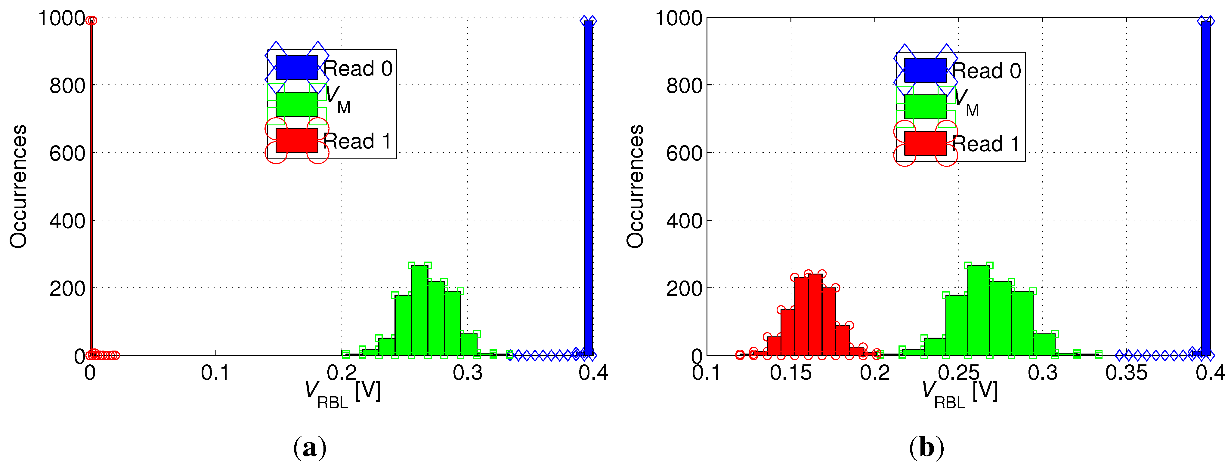
To verify the read-ability of the bitcell, Figure 9 shows the distribution of the RBL voltage ( V RBL ) following read “0” and read “1” operations after the 40 ms retention period. In addition, the figure plots the distribution of the trip-point ( V M ) of the sense buffer. While read “0” is robust in any case (RBL stays precharged), read “1” is most robust if all unselected cells on the same RBL as the selected cell store “0” (see Figure 9(a)), while it becomes more critical if all unselected cells store “1” (see Figure 9(b)), thereby inhibiting the discharge of RBL through the selected cell. This worst-case scenario for a read “1” operation is illustrated in Figure 10(a). In order to make the read operation more robust, V M is shifted to a value higher than V DD / 2 by appropriate transistor sizing in the sense inverter. Ultimately, the V RBL distributions for read “0” and read “1” are clearly separated, and the distribution of V M is shown to comfortably fit between them, as shown in Figure 9.
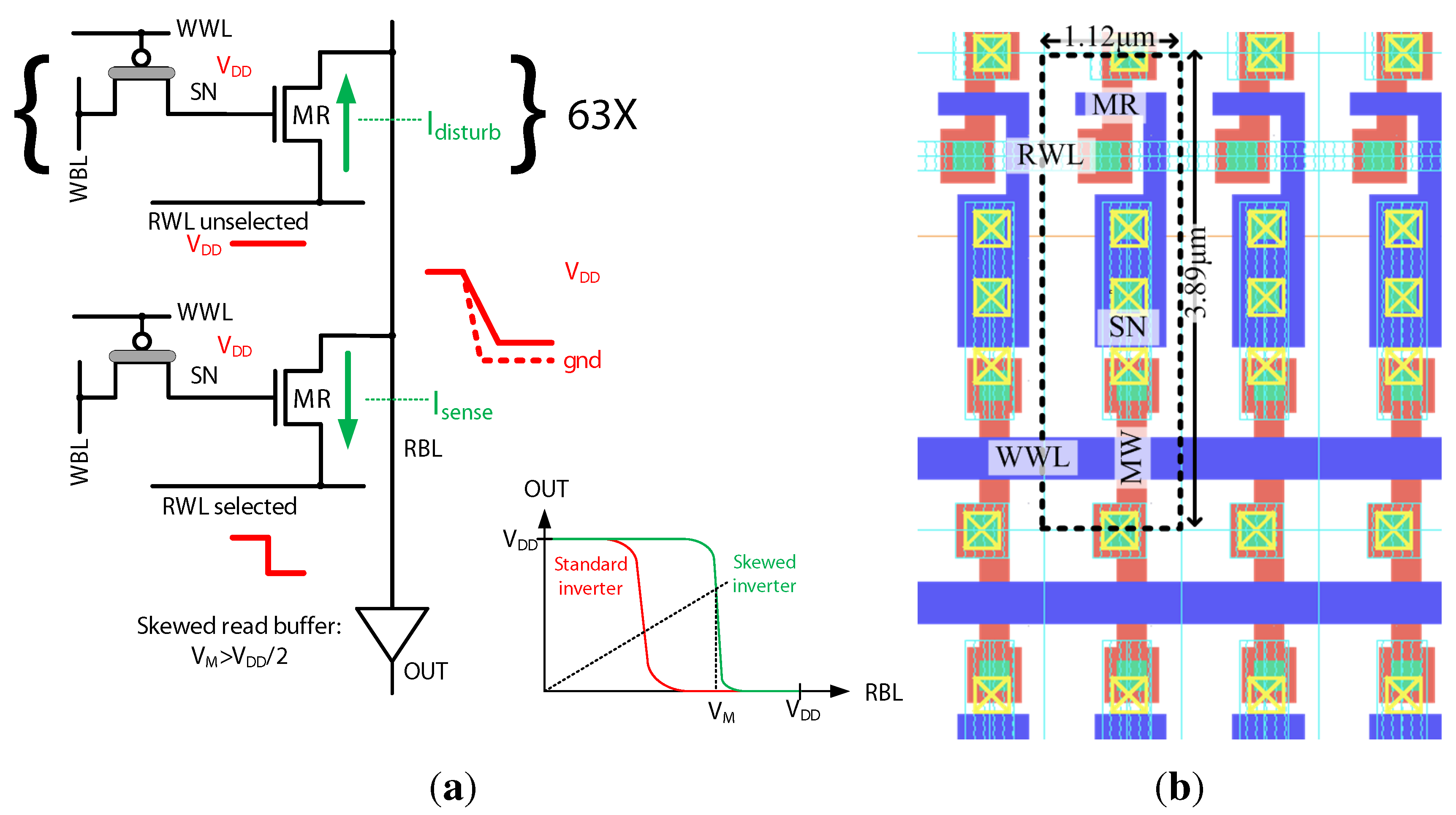
The layout of the 0.18 µm 2T gain-cell, comprising a PMOS I/O MW and an NMOS core MR, is shown in Figure 10(b). The figure presents a zoomed-in view of one bitcell (surrounded by a dashed line) as part of an array. The chosen technology requires rather large design rules for the implementation of I/O devices; however, by sharing the n-well on three sides and stacking the bitlines, a reasonable area of 4.35 µm2 per bitcell is achieved. In the same node, a single-ported 6T SRAM bitcell for above- V T operation has a comparable area cost of 4.1 µm2 (cell violates standard DRC rules), whereas SRAM bitcells optimized for robust operation at low voltages are clearly larger (e.g., the 14T SRAM bitcell in [2] has an area cost of 40 µm2). The depicted layout also enables metal stacking above the storage node to provide an increased SN capacitance of up to 5 fF (see Figure 7(a)).
Figure 9. Distribution of RBL voltage ( V RBL ) after read “1” [circles] and read “0” [diamonds] operations and distribution of the trip-point V M of the read buffer [squares], for (a) favorable and (b) unfavorable read “1” conditions.
Jlpea 03 00054 g009
Figure 10. 180 nm gain-cell array: (a) Worst-case for read “1” operation: all cells in the same column store data “1”; to make the read “1” operation more robust, the sense inverter is skewed, with a trip-point V M > V DD / 2 ; (b) Zoomed-in layout.
Jlpea 03 00054 g010
At an operating frequency of 1 MHz, a full refresh cycle of 64 rows takes approximately 128 µs. With a worst-case 40 ms retention time, the resulting availability for write and read is 99.7%. As summarized in Table 1, the average leakage power of the 2 kb array at room temperature (27 C) is 1.95 nW, while the active refresh power of 1.68 nW is comparable, amounting to a total data retention power of 3.63 nW (or 1.7 pW/bit). This total data retention power is comparable with previous reports on low-voltage gain-cell arrays [13], given for room temperature as well.
Table 1. Figures of Merit.
Technology Node180 nm CMOS40 nm LP CMOS
Number of thin metal layers55
Write TransistorPMOS I/OPMOS HVT
Read TransistorNMOS CoreNMOS SVT
V DDmin 400 mV600 mV
Storage Node Capacitance1.1 fF–4.9 fF0.27 fF–0.72 fF
Bitcell Size1.12 µm × 3.89 µm (4.35 µm2)0.77 µm × 0.42 µm (0.32 µm2)
Array Size64 × 32 (2 kb)64 × 32 (2 kb)
Write Access Time1 µs3 ns
Read Access Time1 µs17 ns
Worst-Case Retention Time40 ms44 µs
Leakage Power1.95 nW (952 fW/bit)68.3 nW (33.4 pW/bit)
Average Active Refresh Energy67 pJ21.2 pJ
Average Active Refresh Power1.68 nW (818 fW/bit)482 nW (235.5 pW/bit)
Average Retention Power3.63 nW (1.7 pW/bit)551 nW (268.9 pW/bit)
Array Availability99.7%97.1%

4. Macrocell Implementation in 40 nm CMOS

Whereas gain-cell implementations in mature technologies have been frequently demonstrated in the recent past, 65 nm CMOS is the most scaled technology in which gain-cells have been reported to date [
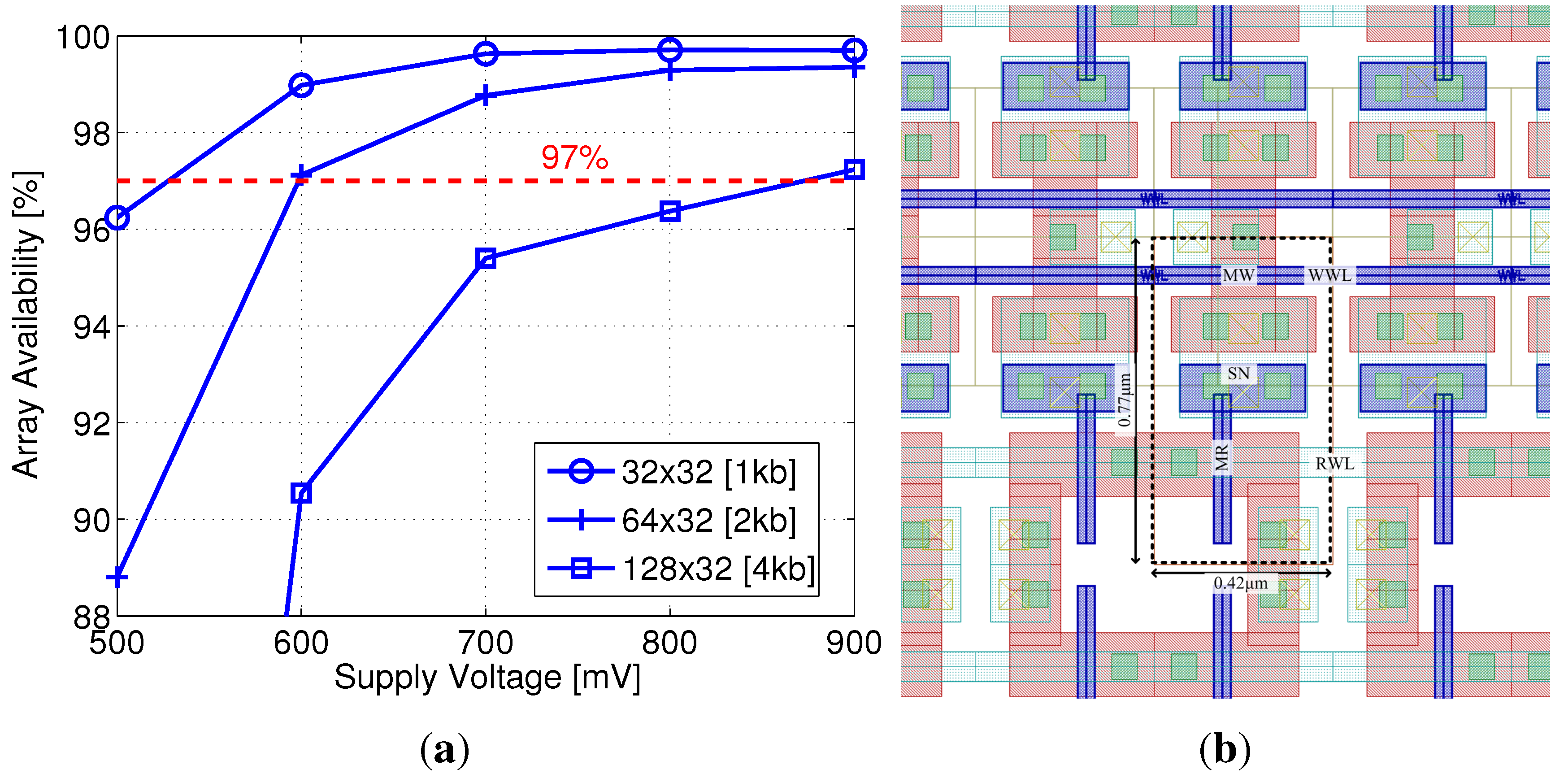
16]. In this section, for the first time, we present a 40 nm gain-cell implementation, and explore array sizes and the corresponding minimum operating voltages that result in sufficient array availability.
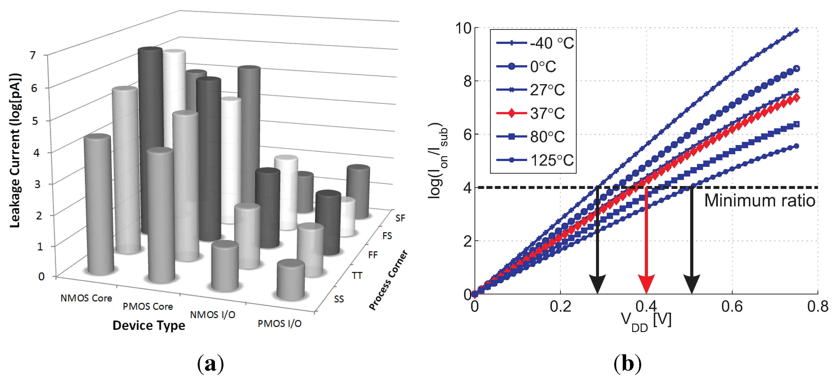
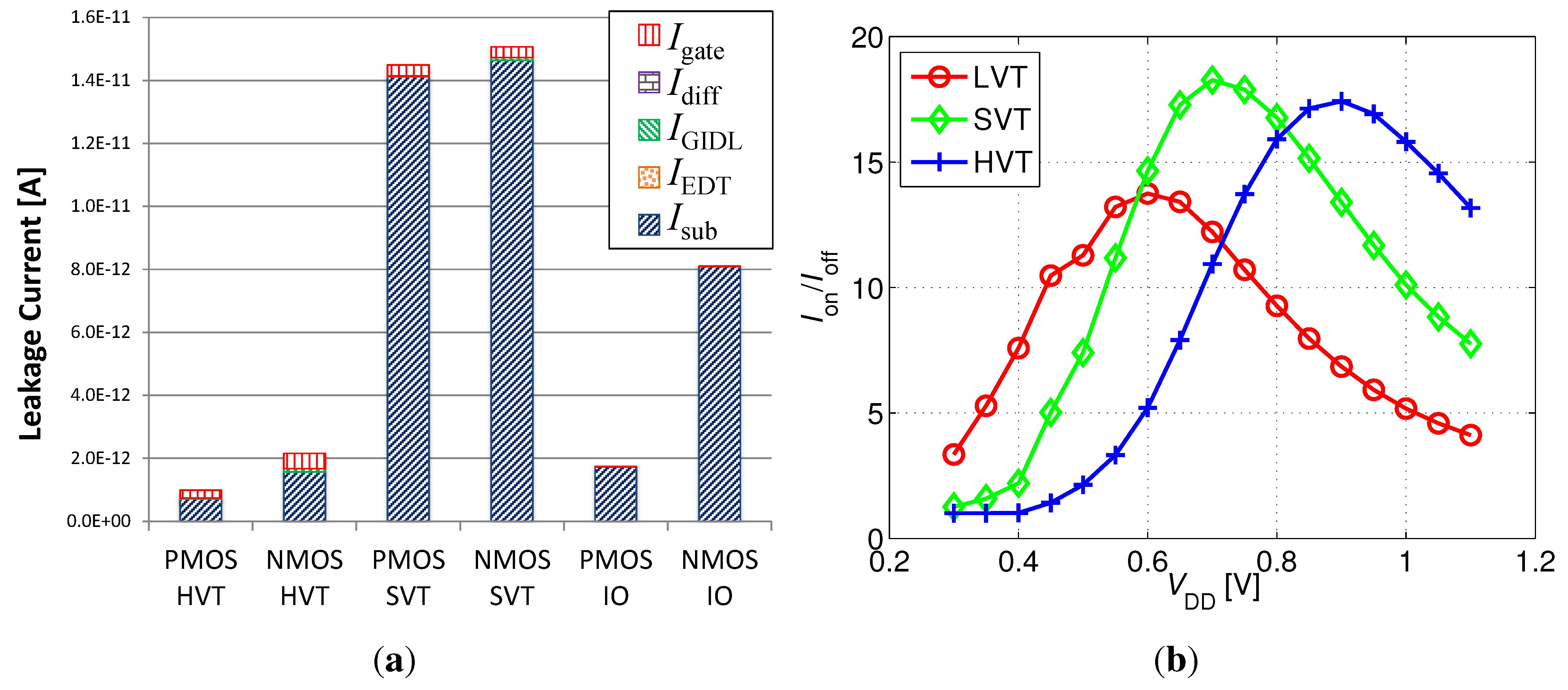
As previously described, core HVT devices are more efficient than I/O devices for write transistor implementation at scaled nodes, providing similar retention times with relaxed design rules (i.e., reduced area). In addition, the multiple threshold-voltage options for core transistors provide an interesting design space for the read transistor selection, trading off on and off currents, depending on supply voltage. Two additional factors that significantly impact the design at scaled nodes are the reduced storage node capacitance, due to smaller cell area and low-k insulation materials, and severely impeded retention times, due to lower storage capacitance and increasing leakage currents. Therefore, array availability becomes a major factor in gain-cell design and supply voltage selection. For this implementation, a minimum array availability of 97% was defined.
Considering a minimum array size of 1 kb (32 × 32), sufficient array availability is unattainable with the LVT MR implementation for a supply voltage lower than 500 mV, suitable for this device according to Figure 5(b). Therefore, an SVT device was considered with near-threshold supply voltages above 500 mV. Figure 11(a) shows the array availability achieved under varying supply voltages, considering array sizes from 1 kb to 4 kb. The red dashed line indicates the target availability of 97%, showing that this benchmark can be achieved with a 2 kb array at 600 mV. At this supply voltage, with a −700 mV underdrive write voltage, the write access time is 3 ns, and the worst-case read access time is 17 ns, while the worst-case retention time is 44 µs (see Table 1). 
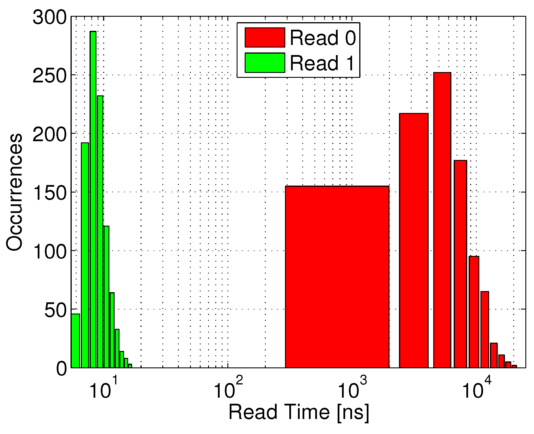
Figure 12 shows the distribution of the time required to sense the discharged voltage of RBL during a read “1” operation following a full retention period (green bars). The red bars (read “0”) represent an incorrect readout, caused by a slow RBL discharge through leakage, such that the read access time must be shorter than the first occurrence of an incorrect read “0”. The clear separation between the two distributions shows that by setting the read access time to 17 ns, the system will be able to robustly differentiate between the two stored states.
Figure 11. 40 nm gain-cell array: (a) Array availability as a function of supply voltage and array size; (b) Zoomed-in layout.
Jlpea 03 00054 g011
Figure 12. Read access time distribution for the 40 nm gain-cell implementation: RBL discharge time for correct data “1” sensing, and undesired RBL discharge time till sensing threshold through leakage for data “0”.
Jlpea 03 00054 g012
A zoomed-in layout of the 40 nm gain-cell array is shown in Figure 11(b), with a bitcell area of 0.32 µm2 (surrounded by the dashed line). For comparison, a single-ported 6T SRAM bitcell in the same node has a slightly larger silicon area of 0.572 µm2, while robust low-voltage SRAM cells are considerably larger (e.g., the 9T SRAM bitcell in [5] has an area cost of 1.058 µm2). As shown in Table 1, the implemented 40 nm array exhibits a leakage power of 68.3 nW, which is clearly higher than for the 0.18 µm array. Even though the active energy for refreshing the entire array is only 21.2 pJ, the required refresh power of 482 nW is again higher than for the 0.18 µm node, due to the three orders-of-magnitude lower retention time. Consequently, the total data retention power is around 150× higher in 40 nm CMOS, compared with 0.18 µm CMOS.

5. Conclusions

This paper investigates two-transistor sub- V T and near- V T gain-cell memories for use in ultra-low-power systems, implemented in two very different technology generations. For mature, above-100 nm CMOS nodes, the main design goals of the bitcell are long retention time and high data integrity. In the considered 0.18 µm CMOS node, a low-leakage I/O PMOS write transistor and an extended storage node capacitance ensure a retention time of at least 40 ms. At low voltages, data integrity is severely threatened by charge injection and capacitive coupling from read and write wordlines. Therefore, the positive storage-node voltage disturb at the culmination of a write operation is counteracted by a negative disturb at the onset of a read operation, which is only possible with an NMOS read transistor. Moreover, the write wordline underdrive voltage must be carefully engineered for proper level transfer at minimum voltage disturb during de-assertion. Monte Carlo simulations of an entire 2 kb memory array, operated at 1 MHz with a 400 mV sub- V T supply voltage, confirm robust write and read operations under global and local variations, as well as a minimum retention time of 40 ms leading to 99.7% availability for read and write. The total data retention power is estimated as 3.63 nW/2 kb, the leakage power and the active refresh power being comparable. The mixed gain-cell with a large I/O PMOS device has a large area cost of 4.35 µm2, compared with an all-PMOS or all-NMOS solution with core devices only.
In more deeply scaled technologies, such as the considered 40 nm CMOS node, subthreshold conduction is still dominant at reduced supply voltages. Gate tunneling and GIDL currents are still small, but of increasing importance, while reverse-biased pn-junction leakage and edge-direct tunneling currents are negligible. In the 40 nm node, the write transistor is best implemented with an HVT core PMOS device, which provides the lowest aggregated leakage current from the storage node, even compared with the I/O PMOS device. A write wordline underdrive voltage of −700mV is employed to ensure strong “0” levels with a short write access time. Among various NMOS read transistor options, an SVT core device maximizes the sense current ratio between a weak “1” and a weak “0” for near- V T supply voltages (600–800 mV) where 97% array availibility is achieved. Both the access times and the retention time are roughly three orders-of-magnitude shorter than in the 0.18 µm CMOS node, due to the increased leakage currents and smaller storage node capacitance. While the active refresh energy is low (21 pJ), the high refresh frequency results in high refresh power (482 nW), dominating the total data retention power (551 nW). As compared with the 0.18 µm CMOS implementation, the scaled down design provides better performance (17 ns read access and 3 ns write access), and a compact bitcell size of 0.32 µm2.
To conclude, this analysis shows the feasibility of sub- V T gain-cell operation for mature process technologies and near- V T operation for a deeply scaled 40 nm process, providing a design methodology for achieving minimum V DD at these two very different nodes.

Acknowledgments

This work was kindly supported by the Swiss National Science Foundation under the project number PP002-119057. Pascal Meinerzhagen is supported by an Intel Ph.D. fellowship. The authors would like to thank Itzik Icin and Meitav Liber for their contribution to this work.

Declaration

Based on “A sub- V T 2T Gain-Cell Memory for Biomedical Applications”, by P. Meinerzhagen, A. Teman, A. Mordakhay, A. Burg, and A. Fish which appeared in the Proceedings of the IEEE 2012 Subthreshold Microelectronics Conference. ©2012 IEEE.

References

  1. Sinangil, M.; Verma, N.; Chandrakasan, A. A Reconfigurable 65 nm SRAM Achieving Voltage Scalability from 0.25–1.2 V and Performance Scalability from 20 kHz–200 MHz. In Proceedings of the IEEE European Solid-State Circuits (ESSCIRC), Edinburgh, UK, 15–19 September 2008.
  2. Hanson, S.; Seok, M.; Lin, Y.S.; Foo, Z.Y.; Kim, D.; Lee, Y.; Liu, N.; Sylvester, D.; Blaauw, D. A low-voltage processor for sensing applications with picowatt standby mode. IEEE J. Solid-State Circuit 2009, 44, 1145–1155. [Google Scholar] [CrossRef]
  3. Constantin, J.; Dogan, A.; Andersson, O.; Meinerzhagen, P.; Rodrigues, J.; Atienza, D.; Burg, A. TamaRISC-CS: An Ultra-Low-Power Application-Specific Processor for Compressed Sensing. In Proceedings of IFIP/IEEE International Conference on Very Large Scale Integration (VLSI-SoC), Santa Cruz, CA, USA, 7–10 October 2012.
  4. Calhoun, B.H.; Chandrakasan, A.P. A 256-kb 65-nm sub-threshold SRAM design for ultra-low-voltage operation. IEEE J. Solid-State Circuit 2007, 42, 680–688. [Google Scholar] [CrossRef]
  5. Teman, A.; Pergament, L.; Cohen, O.; Fish, A. A 250 mV 8 kb 40 nm ultra-low power 9T supply feedback SRAM (SF-SRAM). IEEE J. Solid-State Circuit 2011, 46, 2713–2726. [Google Scholar] [CrossRef]
  6. Meinerzhagen, P.; Andersson, O.; Mohammadi, B.; Sherazi, Y.; Burg, A.; Rodrigues, J. A 500fW/Bit 14fJ/Bit-Access 4 kb Standard-Cell Based Sub-Vt Memory in 65 nm CMOS. In Proceedings of the IEEE European Solid-State Circuits (ESSCIRC), Bordeaux, France, 17–21 September 2012.
  7. Chiu, Y.W.; Lin, J.Y.; Tu, M.H.; Jou, S.J.; Chuang, C.T. 8T Single-Ended Sub-Threshold SRAM with Cross-Point Data-Aware Write Operation. In Proceedings of the IEEE International Symposium on Low Power Electronics and Design (ISLPED), Fukuoka, Japan, 1–3 August 2011.
  8. Sinangil, M.; Verma, N.; Chandrakasan, A. A reconfigurable 8T ultra-dynamic voltage scalable (U-DVS) SRAM in 65 nm CMOS. IEEE J. Solid-State Circuit 2009, 44, 3163–3173. [Google Scholar] [CrossRef]
  9. Teman, A.; Mordakhay, A.; Fish, A. Functionality and stability analysis of a 400 mV quasi-static RAM (QSRAM) bitcell. Microelectron. J. 2013, 44, 236–247. [Google Scholar] [CrossRef]
  10. Hong, S.; Kim, S.; Wee, J.K.; Lee, S. Low-voltage DRAM sensing scheme with offset-cancellation sense amplifier. IEEE J. Solid-State Circuit 2002, 37, 1356–1360. [Google Scholar] [CrossRef]
  11. Chun, K.C.; Jain, P.; Lee, J.H.; Kim, C. A 3T gain cell embedded DRAM utilizing preferential boosting for high density and low power on-die caches. IEEE J. Solid-State Circuit 2011, 46, 1495–1505. [Google Scholar] [CrossRef]
  12. Somasekhar, D.; Ye, Y.; Aseron, P.; Lu, S.L.; Khellah, M.; Howard, J.; Ruhl, G.; Karnik, T.; Borkar, S.; De, V.K.; Keshavarzi, A. 2 GHz 2 Mb 2T Gain-Cell Memory Macro with 128 GB/s Bandwidth in a 65 nm Logic Process. In Proceedings of the IEEE International Solid-State Circuits Conference (ISSCC), San Francisco, CA, USA, 3–7 February 2008.
  13. Lee, Y.; Chen, M.T.; Park, J.; Sylvester, D.; Blaauw, D. A 5.42nW/kB Retention Power Logic-Compatible Embedded DRAM with 2T Dual-Vt Gain Cell for Low Power Sensing Applicaions. In Proceedings of the IEEE Asian Solid State Circuits Conference (A-SSCC), Beijing, China, 8–10 November 2010.
  14. Chun, K.C.; Jain, P.; Kim, C. Logic-Compatible Embedded DRAM Design for Memory Intensive Low Power Systems. In Proceedings of the IEEE International Symposium on Circuits and Systems, Paris, France, 30 May–2 June 2010.
  15. Iqbal, R.; Meinerzhagen, P.; Burg, A. Two-Port Low-Power Gain-Cell Storage Array: Voltage Scaling and Retention Time. In Proceedings of the IEEE International Symposium on Circuits and Systems, Seoul, Korea, 20–23 May 2012.
  16. Teman, A.; Meinerzhagen, P.; Burg, A.; Fish, A. Review and Classification of Gain Cell eDRAM Implementations. In Proceedings of the IEEE Convention of Electrical & Electronics Engineers in Israel, Eilat, Israel, 14–17 November 2012.
  17. Chun, K.C.; Jain, P.; Kim, T.H.; Kim, C. A 667 MHz logic-compatible embedded DRAM featuring an asymmetric 2T gain cell for high speed on-die caches. IEEE J. Solid-State Circuit 2012, 47, 547–559. [Google Scholar] [CrossRef]
  18. Seok, M.; Sylvester, D.; Blaauw, D. Optimal Technology Selection for Minimizing Energy and Variability in Low Voltage Applications. In Proceedings of the ACM/IEEE International Symposium on Low Power Electronics and Design, Bangalore, India, 11–13 August 2008.
  19. Meinerzhagen, P.; Andic, O.; Treichler, J.; Burg, A. Design and Failure Analysis of Logic-Compatible Multilevel Gain-Cell-Based DRAM for Fault-Tolerant VLSI Systems. In Proceedings of the IEEE Great Lakes Symposium on VLSI, Lausanne, Switzerland, 2–4 May 2011.
  20. Meinerzhagen, P.; Teman, A.; Mordakhay, A.; Burg, A.; Fish, A. A Sub-VT 2T Gain-Cell Memory for Biomedical Applications. In Proceedings of the IEEE Subthreshold Microelectronics Conference, Waltham, MA, USA, 9–10 October 2012.
  21. Calhoun, B.; Wang, A.; Chandrakasan, A. Modeling and sizing for minimum energy operation in subthreshold circuits. IEEE J. Solid-State Circuit 2005, 40, 1778–1786. [Google Scholar] [CrossRef]

