Article

Sub-Threshold Standard Cell Sizing Methodology and Library Comparison

1
Electronic System Group, Department of Electrical Engineering, Technische Universiteit Eindhoven, Den Dolech 2, 5612AZ, Eindhoven, The Netherlands
2
Holst Centre/Imec-nl, High Tech Campus 31, 5656AE, Eindhoven, The Netherlands
*
Author to whom correspondence should be addressed.
J. Low Power Electron. Appl. 2013, 3(3), 233-249; https://doi.org/10.3390/jlpea3030233
Submission received: 4 February 2013 / Revised: 29 May 2013 / Accepted: 25 June 2013 / Published: 15 July 2013
(This article belongs to the Special Issue Selected Papers from SubVt 2012 Conference)

Abstract

:
Scaling the voltage to the sub-threshold region is a convincing technique to achieve low power in digital circuits. The problem is that process variability severely impacts the performance of circuits operating in the sub-threshold domain. In this paper, we evaluate the sub-threshold sizing methodology of [1,2] on 40 nm and 90 nm standard cell libraries. The concept of the proposed sizing methodology consists of balancing the mean of the sub-threshold current of the equivalent N and P networks. In this paper, the equivalent N and P networks are derived based on the best and worst case transition times. The slack available in the best-case timing arc is reduced by using smaller transistors on that path, while the timing of the worst-case timing arc is improved by using bigger transistors. The optimization is done such that the overall area remains constant with regard to the area before optimization. Two sizing styles are applied, one is based on both transistor width and length tuning, and the other one is based on width tuning only. Compared to super-threshold libraries, at 0.3 V, the proposed libraries achieve 49% and 89% average cell timing improvement and 55% and 31% power delay product improvement at 40 nm and 90 nm respectively. From ITC (International Test Conference 99) benchmark circuit synthesis results, at 0.3 V the proposed library achieves up to 52% timing improvement and 53% power savings in the 40 nm technology node.

1. Introduction

Low voltage digital design, especially near/sub-threshold design, is becoming more popular in application domains where performance is not the primary concern. More and more systems with low performance requirements are operated from a near/sub-threshold supply voltage in order to save power [3,4,5,6,7]. However, due to the fact that the gate voltage drive of the transistors operating in the sub-threshold domain is small, standard logic cells become more sensitive to process variations. Commercial cell libraries are designed and characterized for super-threshold voltage operation. Without any optimization, most cells of such conventional libraries will not have a robust operation in the presence of process variability at a low operating voltage. Therefore, careful sizing of standard cells working at low voltage is needed. In [1], the optimization procedures to size standard cells are explained. In [2], the standard cell libraries optimized for sub-threshold operation are presented. This paper extends the work of [1,2]. Here, the sizing methodology and sizing methods are explained using a CMOS 40 nm low power process as an example. Benchmarking of the libraries is carried out using both a CMOS 90 nm and a CMOS 40 nm low power process. ITC benchmark circuit synthesis results are presented as well.
Unlike conventional “super-threshold” cell sizing methods [8,9], the proposed balancing-based sizing method focuses on the statistical distribution of the drain-source current, rather than the current itself. In the proposed approach, the variation of the current is taken into consideration when sizing the standard cells by balancing the mean current of the equivalent N and P networks. The way of finding the equivalent N and P networks is based on timing arcs. The transition paths within the standard cells are different for distinct input patterns. The longest path, which has the worst delay, is defined as the worst-case transition path; the shortest path, which has the best delay, is defined as the best-case transition path. The transistors of the worst-case and the best-case transition paths are balanced in two possible ways: (i) transistor width and length tuning; and (ii) transistor width tuning only. In one case both the channel length and width of the transistor are optimized to have a better performance at low voltages, since in the sub-threshold regime, increasing the channel length has a positive impact on timing and timing variation [8]. Therefore, by increasing the transistor’s length and by tuning the width [10] we are able to size the cells in the sub-threshold regime with two degrees of freedom. The second optimization approach, width tuning only, targets better timing and variation from the sub-threshold to the super-threshold regions.
Taking into account transistor sizing effects in sub-threshold [8], the balancing-based cell sizing methodology is presented in Section 2. Moreover, Section 2 also explains the standard cell optimization methods and how they can be applied to complex cells. A 163 standard cells library was designed and characterized using the proposed sizing methods in two technology nodes; the results are shown in Section 3. The evaluation of these libraries is presented in Section 4. Furthermore, to benchmark the libraries in the 40 nm technology node, ITC benchmark circuits are used to test the performance and variability of different libraries. The results are shown in Section 5. Section 6 concludes the paper.

2. Sub-Threshold Cell Sizing Methodology

Several relevant research results have been presented about sub-threshold sizing. In [3,4], the authors calculate the optimum supply voltage to minimize energy consumption. It is also claimed that, theoretically, minimum sized cells are optimal for energy reduction. In this paper it is shown that under speed constraints, and when process variability is taken into account, this is not the case. In [11], the authors explain the benefit of technology choices, power supply scaling, and body bias adaptability for circuits working in the sub-threshold regime. It is implied that standard cell timing could be improved using the mentioned design techniques. The concept of sub-threshold logical effort for complex gate sizing is presented in [9]. Particularly interesting is a closed form current equation derived for stacked transistors in relation to other transistors in the same stack. Compared to [3,4,9], our sizing approach focuses on narrowing the current/delay distribution spread and on increasing the performance through a new balancing theory that slows down fast transistors and vice versa. In [8], the transistor reverse short channel effect (RSCE) is used for device sizing optimization, where the channel length is increased to have an optimal threshold voltage which makes the transistors have a higher current, be less sensitive to random variations, and to have a smaller area. With a higher current and a lower gate capacitance, the delay and power are both reduced. Furthermore, in [8], the channel lengths of the NMOS and PMOS are increased to achieve the maximum currents for both NMOS and PMOS transistors. Unlike [8], our sizing optimization does not always lead to the maximum active current for both the NMOS and PMOS transistors. Only the transistors on slower timing arcs are allowed to be upsized, the ones on faster timing arcs are down sized to save area. In [12], a standard cell library in 65 nm is presented, where by upsizing the channel length of all transistors in a given cell, the energy per operation value is reduced by about 15%. In this paper, the standard cells are tuned individually, with various length and width selections to have balanced transition currents. Reference [13] presents a searching algorithm based on multiple objectives through a free space search to optimize one cell. The approach is exhaustive and suitable for single cells, but the searching effort is very large for a complete library. Unlike [11], our optimization targets balancing the mean P and N currents and takes into account the impact of process spread. In [14], a 45 nm standard cell library optimized for 0.35 V is proposed. The proposed PMOS-to-NMOS transistor ratio optimization is based on the optimal energy-delay product, not on balanced rise and fall times. In our work, the rise and fall times are balanced taking into account the effect of process variations.
Overall, in this section, a new statistical formulation [1] to size standard cells is introduced. The differences of the proposed work from other sizing methods are that in our work, the threshold voltage variation is treated as one of the statistical parameters in the current/delay equation, and the cells are optimized to have balanced current/delay distributions. The proposed sizing approach is derived from the observation that the transistor’s current distribution in the sub-threshold regime follows a Log-Normal spreading, whereas conventional sizing treats the transistor’s current as a Normal distribution. Considering the above-mentioned fact and the observation that process variability can be mapped onto threshold voltage variability with a first order approximation, a balancing based sizing methodology is developed for robust standard cell design.

2.1. Sub-Threshold Current Distribution Model

The sub-threshold region is often called the weak inversion region [15], partly because in the sub-threshold region, the transistor is neither completely turned on nor turned off. In digital circuits, the sub-threshold current is the parasitic leakage, ideally zero. By reducing the voltage supply to sub-threshold, and by letting the transistor operate in weak inversion, the power consumption can be reduced quadratically [16]. Transistors operating in the sub-threshold regime obey an exponential dependence on the gate drive voltage [8]:
Jlpea 03 00233 i001
where Jlpea 03 00233 i002 
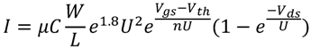
is the mobility; C is the oxide capacitance; Jlpea 03 00233 i003 the sub-threshold slope factor; and U is the thermal voltage. Jlpea 03 00233 i004 is the gate to source voltage; Jlpea 03 00233 i005 is the drain to source voltage; Jlpea 03 00233 i006 is the threshold voltage, consists of zero biasing voltage, terminal voltages and device size effects [17]. From Equation (1), one can see that the current has an exponential relationship with the gate-to-source voltage and the threshold voltage of the transistor.
In sub-threshold, the probability distribution function (PDF) of the current obeys a Log Normal distribution. If the supply voltage is reduced to the sub-threshold level, the widely distributed current will lead to a wide transistor delay spread. Therefore, an optimization based on a super-threshold current distribution will not guarantee a robust behavior in the sub-threshold regime. We consider the Jlpea 03 00233 i006 as a Normal distribution and model the distribution of the transistor current using [18,19] as follows:
Jlpea 03 00233 i007
where Jlpea 03 00233 i008 
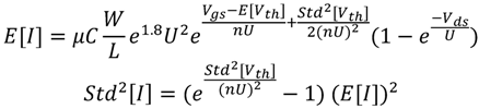
stands for the mean value and Jlpea 03 00233 i009 stands for the standard deviation. In this model Jlpea 03 00233 i010 and Jlpea 03 00233 i011 are regarded as technology parameters for a given W and L set. With the width and length tuning, Jlpea 03 00233 i010 and Jlpea 03 00233 i011 also change accordingly due to RSCE. Therefore, depending on the range of W and L , different distributions of the Jlpea 03 00233 i006 are used in the sizing model.

2.2. Sub-Threshold Cell Balancing Method

In traditional CMOS design, the transistor geometry ratio (W/L) of the pull-up PMOS network to the pull-down NMOS network is carefully tuned to compensate for the difference between the mobility of electrons and holes. This ratio is derived from balancing the rise/fall-time delays and minimizing the propagation delay.
In sub-threshold, it is more about equalizing the strength of the pull-up and the pull-down network that directly affects the functional correctness and the minimum Jlpea 03 00233 i012. In the proposed sizing methodology, the ratio of the pull-up to pull-down transistors is determined by the balance between the current distributions of the PMOS and NMOS transistors. The difference with regard to the conventional sizing approach is that the current spread caused by the Jlpea 03 00233 i013 variation is taken into account.
The proposed sizing methodology includes a transition-based approach in which the worst rise and fall times are improved by compromising the best rise and fall times. In this way, there is more room to improve the worst-case performance of the cells without area penalty.
Basically, the mean currents of the PMOS and NMOS networks are made equal, i.e., Jlpea 03 00233 i014. From this, one can derive [1]:
Jlpea 03 00233 i015
where Jlpea 03 00233 i016 
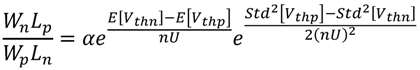
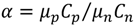
is a technology parameter defined by the mobility and oxide capacitance of the NMOS and PMOS transistors. Jlpea 03 00233 i017 is also used as the conventional sizing factor. Given the Jlpea 03 00233 i006 mean and variance values, Equation (3) serves as the current balancing equation. The NMOS and PMOS current distributions can be closely matched based on Equation (3).
Figure 1 displays results of Monte Carlo simulations (CMOS 40 nm, 0.3 V power supply) of the normalized active current distributions of the NMOS and PMOS transistors of an inverter of strength 2 (INVD2). In the remaining of the paper the same commercial CMOS 40 nm technology is used as a reference. The current distributions of the NMOS and PMOS transistors can be closely matched, following Equation (3). Before balancing, the widths of the NMOS/PMOS are 0.62 μm/0.82 μm with fixed length of 0.041 μm. After balancing, the widths are 0.31 μm/0.60 μm and the lengths are 0.1 μm/0.044 μm, respectively. Note that the current distribution of the PMOS transistor is improved whereas the current of the NMOS transistor is weakened. In this case, the worst-case current distribution of the INVD2 is improved by reducing the best-case current. After the current balancing, the area of the INVD2 stays the same as before the balancing method is applied.
Figure 1. Normalized transistor current distributions in CMOS 40 nm. (a) Current distribution before balancing; (b) current distribution after balancing.
Jlpea 03 00233 g001
This balancing equation allows us to balance the rise and fall current distribution of the inverters without area penalty.

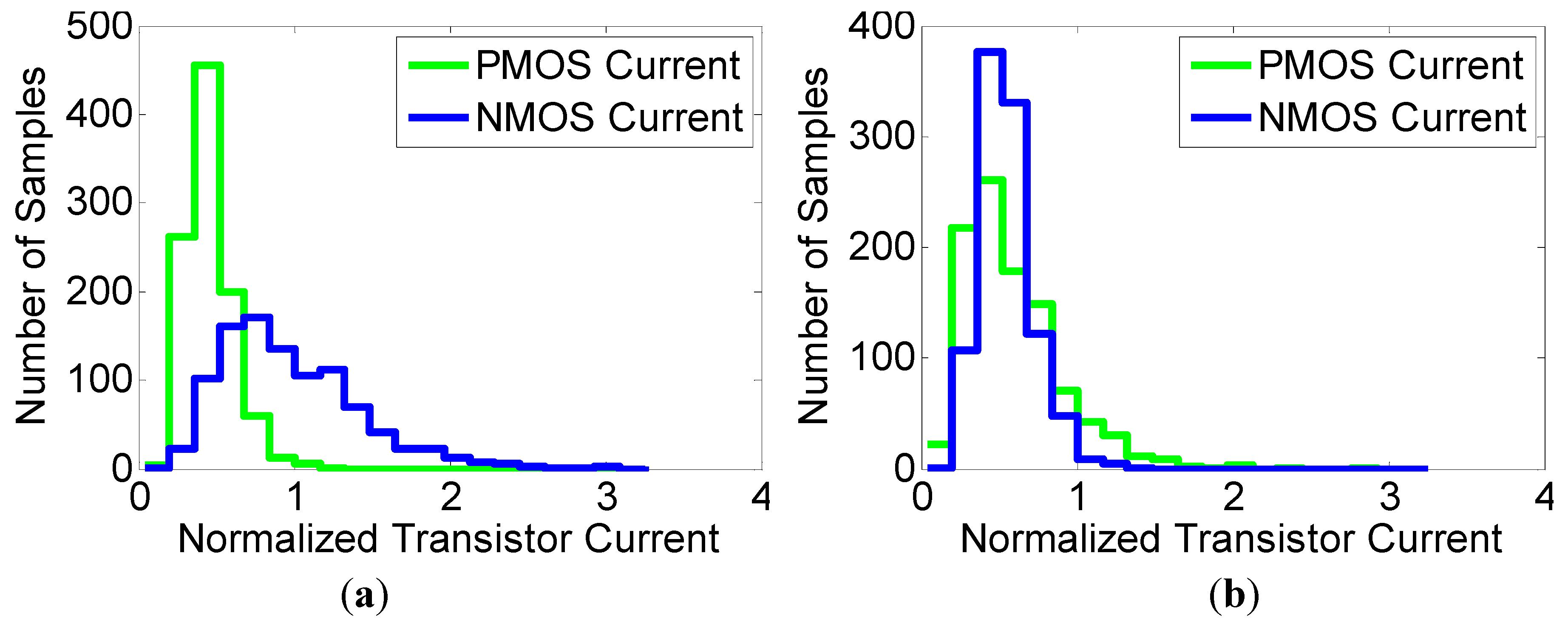
2.3. Stack Sizing Model

The magnitude of the current flowing through a transistor stack depends on the number of transistors and the size of each transistor. Without loss of generality, consider a transistor stack as depicted in Figure 2.
Figure 2. PMOS stack schematic.
Jlpea 03 00233 g002
Let us enumerate this stack of PMOS transistors in descending order as a function of their proximity to the power supply VDD. Similarly, consider a stack of NMOS transistors enumerated as a function of their proximity to Ground. Simulation results show that the upper Jlpea 03 00233 i020 
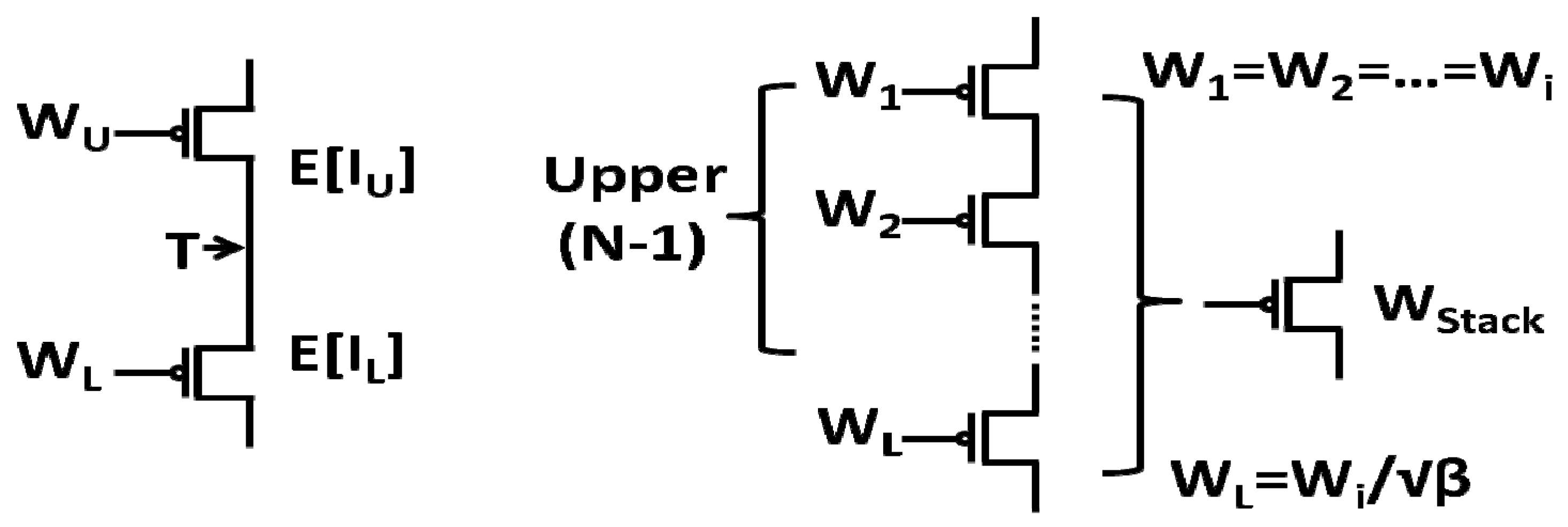
PMOS transistors [lower Jlpea 03 00233 i021 NMOS transistors] have a similar impact on the current behavior of the stack. Therefore, let these Jlpea 03 00233 i020 transistors have equal sizes. Using the results of [9,20] to calculate the equivalent transistor width of the stack, Jlpea 03 00233 i022, the mean current of Jlpea 03 00233 i023 transistors in a stack is calculated as follows [1]
Jlpea 03 00233 i024
where Jlpea 03 00233 i025 
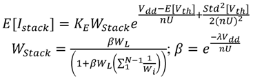
is a technology fitting parameter and λ is the DIBL effect coefficient [9]. To simplify the calculation of the equivalent transistor size of the stack, the length of each transistor in the stack is held fixed. Let the width of all Jlpea 03 00233 i026 transistors be Jlpea 03 00233 i027 and the width of the remaining transistor be Jlpea 03 00233 i028, as shown in Figure 2. The width of the equivalent transistor is denoted as to Jlpea 03 00233 i029. The same procedure holds for NMOS transistors.
The variance of the stack is determined by the variance of each transistor in the stack. Since each transistor has the same impact on the total variance, the stack variance is the sum of the variances of each transistor divided by the square of the number of transistors in the stack [18].
Jlpea 03 00233 i030
where Jlpea 03 00233 i031 
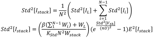
is also a technology dependent fitting parameter. With Equations (4) and (5), one can easily derive the optimal stack width ratio for the stack’s maximum current or minimum current spread. To achieve the maximum current, the lower PMOS (upper NMOS) transistor needs to be sized Jlpea 03 00233 i032 times smaller with regard to the upper PMOS (lower NMOS) transistors. The variation of the current stack can be written as:
Jlpea 03 00233 i033
Equation (6) helps to understand how many transistors can be stacked for given current variation and area constraints. Ultimately, this is a very important criterion for robust operation. To quantify this observation, 3000 Monte-Carlo simulations were run for 2, 3, 4, and 5 NMOS transistors in a stack working at 0.3 V and at room temperature (unless mentioned all the Monte-Carlo simulations are at 0.3 V and at room temperature). The results are shown in Table 1. The length of each transistor is held fixed to 0.04 μm, and the total width for each simulation set-up is set to 3 μm to keep the area constant. In Table 1 it is shown that Equation (6) predicts correctly the trend of the variation. The mismatch between the calculation and the simulation values is because Jlpea 03 00233 i034 
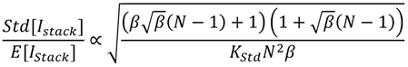
variation is treated as a given technology dependent parameter for given sizing (source bulk modulation is not taken into account). Table 1 is also an indicator of the large current variability when many transistors stacked transistors are used in the sub-threshold regime.
Table 1. Current variation in series-connected transistors @ 40 nm.
Number of transistors in seriesSimulation resultsNormalized Jlpea 03 00233 i035Calculation from Equation (6)
Jlpea 03 00233 i036 (A) Jlpea 03 00233 i035
2 × 0.50 μm2.31 × 10−842.35%11
3 × 0.33 μm1.39 × 10−853.03%1.2521.237
4 × 0.25 μm1.11 × 10−858.68%1.3861.401
5 × 0.20 μm0.95 × 10−866.18%1.5631.573

2.4. Parallel Sizing Model

The resulting PDF current of N parallel-connected transistors is the sum of their Log-Normal current distributions. The sum of Log-Normal distributions with the same variance can be approximated by one Log-Normal distribution [21]. A correlation factor Jlpea 03 00233 i037 for Jlpea 03 00233 i034 needs to be introduced to improve the accuracy of the model. This correlation factor was not needed in series-connected transistors because in that case the source-bulk modulation overshadows the correlation. The mean and variance of the current of N identical parallel connected transistors is [1]
Jlpea 03 00233 i038
where Jlpea 03 00233 i039 
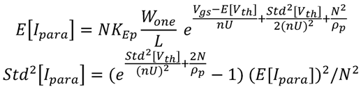
is the width of one single transistor,
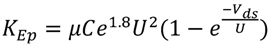
 Jlpea 03 00233 i040 and Jlpea 03 00233 i041
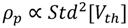
. The equivalent width for parallel transistors can be calculated from Equation (7) [1].
Jlpea 03 00233 i042
Hence the width of a single transistor, which has the same mean current as the one of N transistors in parallel, is Jlpea 03 00233 i043 
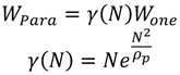
times the width of the transistors in parallel.
To quantify our model, 3000 Monte-Carlo simulations were run for 1 to 6 NMOS transistors connected in parallel, with a total width of 1.20 μm. The simulation and calculation results are shown in Table 2. It is worth observing these results in more detail [22]. Namely, the joint correlated Log-Normal distribution indicates that the mean current is bigger than that of the uncorrelated sum of individual transistor currents [18,21]. This implies that for the sub-threshold regime it could be advantageous to layout parallel-connected transistors as the current drive is higher.
Table 2. Mean current of parallel-connected transistors in CMOS 40 nm.
Number of parallel transistors Simulated Jlpea 03 00233 i036 (A)Normalized Jlpea 03 00233 i036Calculation from Equation (7)
1 × 1.20 μm1.18 × 10−71.001.00
2 × 0.60 μm1.33 × 10−71.131.12
3 × 0.40 μm1.41 × 10−71.191.24
4 × 0.30 μm1.52 × 10−71.291.36
5 × 0.24 μm1.71 × 10−71.451.48
6 × 0.20 μm1.91 × 10−71.621.61

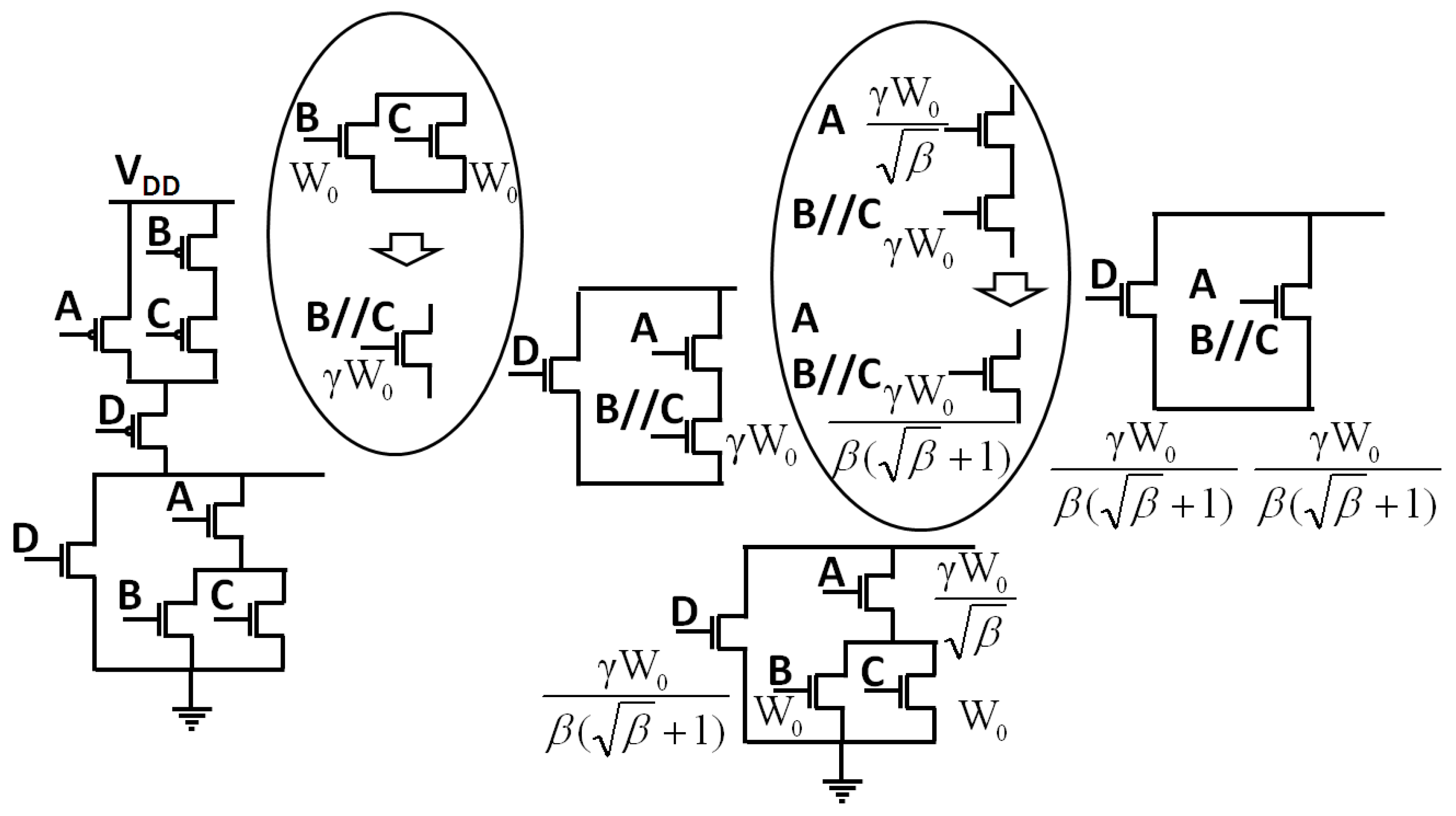
2.5. Complex Cell Translation

Complex cells can be sized by finding equivalent transistor sizes from reducing stack and parallel arrangements to their equivalent reference transistors. Note that when the stack or parallel arrangement is reduced to the equivalent reference transistors, the distribution parameters, the mean and standard deviation of the arrangements are also calculated by the equations shown above.
Without loss of generality, a complex cell as the one depicted in the left part of Figure 3 is used to explain how the cell is “reduced”. The equivalent sizes of the transistors in series or parallel connection can be determined by two rules as depicted in
Algorithm 1.
1. If n transistors in Parallel
2. Then Size of parallel transistors:
3. W1 = W2 = … = Wn
4. Parallel Equivalent Size: Equation (8)
5. If m transistors in Series
6. Then Size of transistors in stack:
7.  Jlpea 03 00233 i044
8. Stack Equivalent Size: Equation (4)
9. *U means next to output node; L means away from output node.
Figure 3. Complex cell translation example.
Jlpea 03 00233 g003
In the right part of Figure 3, the NMOS network is used as an example to show how the sizing ratio is determined by two If-Then rules. The translation starts with the parallel-connected NMOS transistor B and C. The initial sizes of size of B and C are equal to Jlpea 03 00233 i045 as the unit size of the N network. Then, the size of the equivalent transistor of B // C is Jlpea 03 00233 i046 according to Equation (8). With transistor A in series connection, the size of A can be defined by the second if then rule, as Jlpea 03 00233 i047. The equivalent size of A, B // C is defined by Equation (4) as Jlpea 03 00233 i048. The size of transistor D is equal to the size of the equivalent parallel-connected transistors. A similar procedure can be followed to size the transistors of the P network.
The sizing approach that we just outlined can guarantee the maximum PDF current within the N/P networks. The immediate follow up step is to balance the fall and rise delays across the N/P networks according to Equation (3). For the transistors shown in Figure 3, the balancing Equation (3) is applied between the worst-timing transition path in the N network (transistors A and C) and the best-timing transition path in the P network (transistors A and D), and between the best-timing transition path in the N network (transistor D) and the worst-timing transition path in the P network (transistors B, C, and D). The equivalent transistor of the transistors on the best/worst timing transition path within N/P network is determined by Equations (4) and (8). For example, consider the worst-timing transition path in the N network consisting of transistors A and C. Following Equation (4), we substitute Jlpea 03 00233 i049 for Jlpea 03 00233 i027 and Jlpea 03 00233 i050 for Jlpea 03 00233 i051. Then, the equivalent size of the worst-timing transition path in the N network becomes Jlpea 03 00233 i052. This is balanced against the equivalent transistor resulting from the best timing transition path in the P network using Equation (3) to find the actual width values of Jlpea 03 00233 i053 for the N and P networks. Other combinations of equivalent transistors on the best/worst timing transition path of the N/P network can be derived accordingly.
In this paper the libraries are targeted at balancing the worst-case rise and fall transitions.
When both width tuning and channel length tuning are considered, the library performs well at near threshold supply voltages [13]. For higher supply voltages, the benefit of having non-minimum channel length decreases. On the other hand, the library in which only width optimization is used has a constant improvement over a wide voltage ranges as compared to the reference library. Therefore, the former should be used for digital blocks mainly operating in sub-threshold region, while the latter should be used for blocks, which are working in a wide voltage range from sub-threshold voltage to nominal supply voltage. The cell area constraint is set to be the same for both libraries and equal to the corresponding “super-threshold” cell area. The differences are only on individual transistor sizes, so there is no extra area cost.

3. Library Characterization

To benchmark the sizing methods, all libraries (two at 40 nm technology and three at 90 nm technology) are characterized for worst-case timing and power from 0.3 V to 1.2 V in 0.1 V steps based on the layout extracted standard cell netlists (including parasitic). As the super-threshold cells will not function properly under 0.3 V, 0.3 V is set as the lowest characterization voltage to have a fair comparison with the proposed libraries. The characterization is done in SS process corner at room temperature with slew and loading ranges appropriate to the supply voltage. Since the area is constrained to be the same as the corresponding super-threshold libraries, the loading stays the same as the one in the super-threshold libraries. To define the slew range, a single drive strength inverter with loading specified by the commercial super-threshold libraries is simulated. The appropriate slew for each voltage is determined by matching rise/fall times of the input node and fall/rise times of the output node respectively.
Both ELC and Altos of Cadence are used for library re-characterization. Altos is used for the 40 nm library, and ELC is used for the 90 nm one. The simulation engine is Spectre. The results of the library characterization are stored according to the commercial liberty format [23]. The timing information of each pin of each cell is presented in four matrices: rise time represents the rising slew, rise transition represents the transition time when the output rises. Similarly, fall time and fall transition represent the delay when the output falls. The characterized libraries follow a 7 × 7 timing and power template. Each matrix consists of 49 values for seven different slew times and seven loading parameters. A similar format also applies to power information.

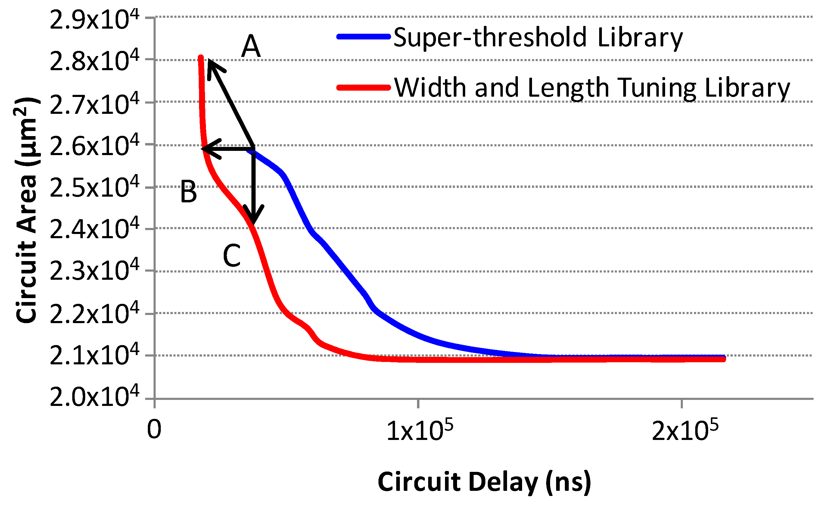
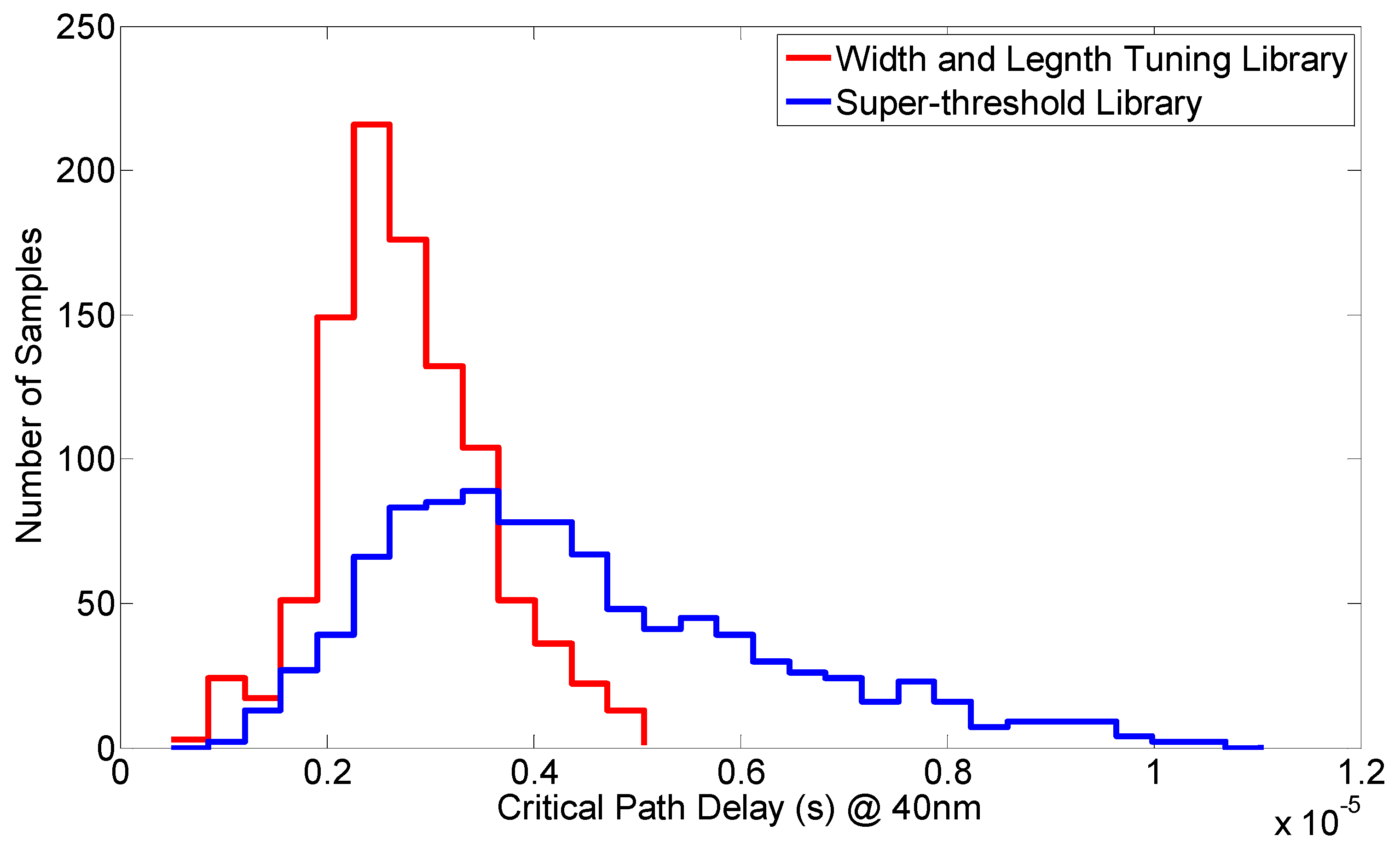
4. Library Comparisons

Since the values of slew and loading parameters differ over two orders of magnitude in these matrices, it is not convenient to carry out a straightforward comparison. Instead, the average value of each matrix is used to represent the delay and power, called as pin-delay and pin-power parametric.
The pin-delay and pin-power values are used to compare the proposed sub-threshold libraries to the “super-threshold” library at different voltages. The comparisons are carried out on a CMOS 90 nm and on a CMOS 40 nm SVT technology. In Figure 4, the voltage scalability of different libraries at 90 nm is presented. Timing improvement is calculated by comparing the delay value of each cell in sub-threshold to the corresponding cell in the super-threshold library, and the average of all improvements are compared. The library with width and length tuning shows around 49% better timing at 0.3 V, and when the voltage increases to 0.65 V, the improvement drops to 0. Above 0.65 V the library with width and length tuning works slower than the “super-threshold” library. The library with width tuning only shows 10% to 11% better average timing from 0.3 V to 1.2 V compared to the “super-threshold” library.
Figure 4. Average cell timing improvement of different voltages in CMOS 90 nm.
Jlpea 03 00233 g004
In Figure 5, the width and length tuning library is compared to the “super-threshold” library at 0.3 V. The max cell delay is the maximum value of the pin-delay of each cell. It actually shows the worst average transition of each cell. The corresponding pin-delay and pin-power are used to compare the power delay product (PDP) of each cell. The max cell and the max cell PDP are compared in each technology node.
Figure 5. Normalized max cell delay and PDP comparison in CMOS 90 nm and 40 nm. (a) Delay comparison at 90nm; (b) PDP comparison at 90nm; (c) delay comparison at 40nm; (d) PDP comparison at 40nm
Jlpea 03 00233 g005
One can see that most of the cells from the width and length tuning library lie above the reference 45 degree dashed line, which means that the cells from the width and length tuning library have better timing properties. Those cells that lie on the reference line are the minimum sized cells, which cannot be further optimized using the proposed balancing-based sizing method. Following the proposed sizing method, the complex cells and cells with larger drive strength have better performance compared to the rest of the logic cells.
On average, the 90 nm cells with width and length tuning have 38% better timing for worst case transitions without introducing extra area cost. On average the cells from the width and length tuning library achieve 31% better PDP at worst transition. In the 40 nm technology node, the width and length tuning library cells have 49% average timing improvement for worst-case transitions and 55% better average PDP compare to the super-threshold library reference at 40 nm.
Three thousand Monte Carlo simulations have been done for each cell to compare their timing variation at 0.3 V. The results of the delay, variation and area of the cells are shown in Figure 6. The marker size shows the area of the cell. As known, bigger cells have less variation [24]. However, in the figure, this is not always true for all the cells; most of the cells lie in the standard deviation/mean range from 50% to 70%. There is no clear indication that, increasing the area will lead to variation savings in the sub-threshold region.
In Figure 6, we see that our cells are mainly distributed in the lower left corner, which means that the performance and the robustness of our cells are better than the cells of the super-threshold library, as expected. On average, the cells that follow the width and length tuning method have 11% variation savings and 2.17× performance improvement at 40 nm. Among all the cells compared, the width and length tuning have maximally 45% variation savings for a two input NOR gate NR2D1 and 4.12× maximum performance improvement for the NR2XD8 without any area penalty.
Figure 6. CMOS 40 nm libraries cell delay variation and area comparison at 0.3 V. The values in the figure are normalized to the minimum mean delay of each super-threshold library.
Jlpea 03 00233 g006

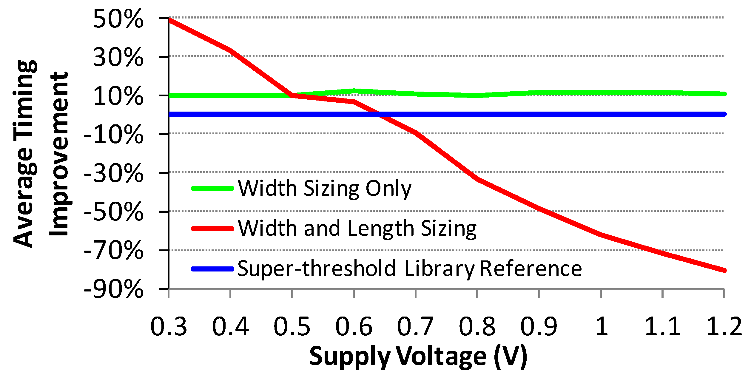
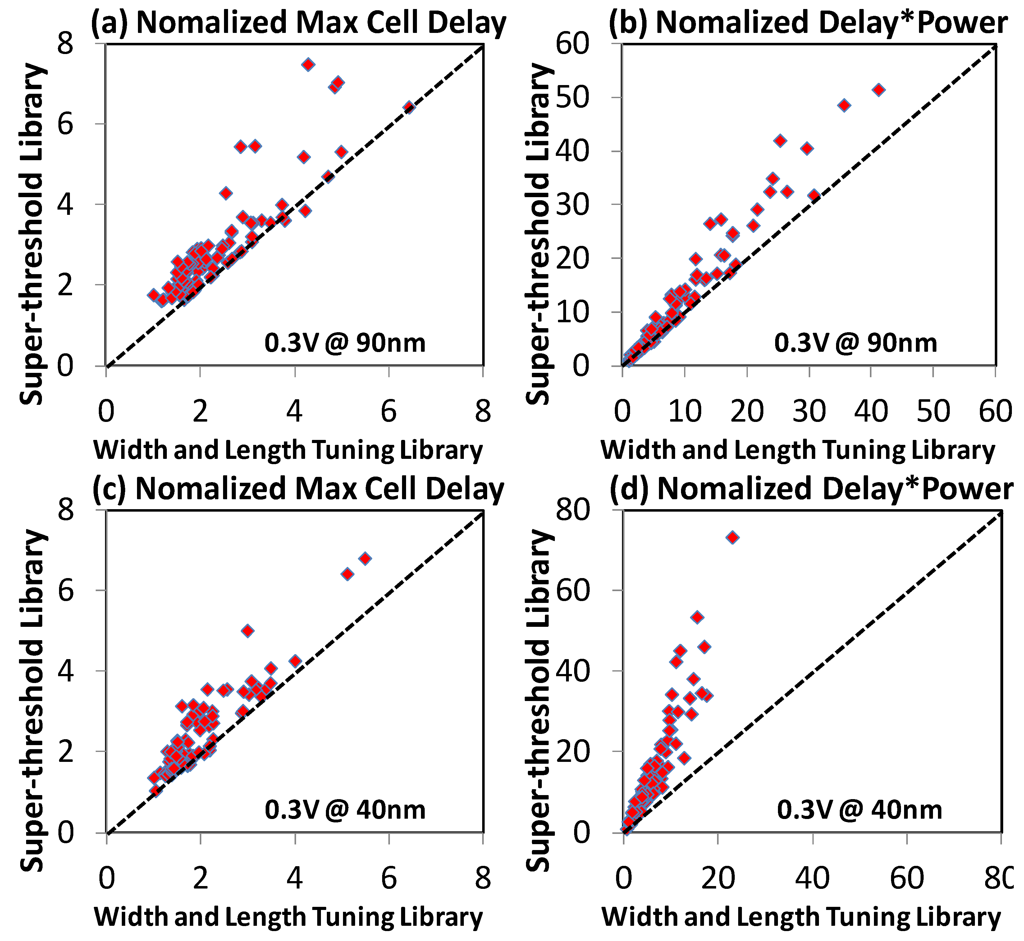
5. Circuit Synthesis Comparisons

5.1. ITC B14 Benchmark

We look here first in detail at synthesis results of the B14 circuit from ITC benchmark circuit [25].
We extracted the critical paths generated by each different library at 0.3 V, and then applied 1000 Monte Carlo simulations are used to generate the delay distributions of each critical path to compare the variability of different libraries. The results are shown in Figure 7.
Figure 7. Critical path delay distribution comparisons in CMOS 40 nm.
Jlpea 03 00233 g007
As can be seen from Figure 7, the critical path delay follows a Log-Normal distribution. Without any sizing optimization, the critical path has a wide distribution with a long tail as the blue line shows. One can see that the delay distribution of the critical path of the proposed library cells is left shifted and narrowed down, where the mean delay decreases from 4.25 μs to 2.59 μs, and the variation is reduced from 44% to 30%.
In Figure 8, the synthesized delay versus area trend at 0.3 V is compared. The three black arrows show different constraints. With the width and length-tuning library, the circuit can work at faster speed. Arrow C indicates that, when delay is a constrain, the circuit synthesized by the width and length tuning library requires 14% less area as compared to the circuit synthesized with the super-threshold library. When area is the constraint (arrow B), the circuit synthesized by the width and length-tuning library is 1.8× faster. Without any constraints, the circuit can be sped up 2.1× with 1.08× area compared to the circuit synthesized by the super-threshold library, as indicated by arrow A.
Figure 8. Synthesized circuit delay and area comparison in CMOS 40 nm at 0.3 V.
Jlpea 03 00233 g008

5.2. ITC Benchmark Circuits

ITC benchmark circuits [25] were synthesized for minimum delay to compare 40 nm libraries at 0.3 V. The delay, area, and power information are shown in Table 3, Table 4, Table 5. In Table 3, the speed of the circuit synthesized by the proposed library is pushed to the highest possible value like the arrow A in Figure 8. Table 4 shows the delay improvement and power savings when the area is constrained as arrow B in Figure 8. Table 5 shows the area and power saving when the same target delay is applied as the arrow C in Figure 8.
Table 3. ITC benchmark circuit synthesis results.
Delay (ns)%Area (μm2)%Total Power (nW)%
Super-threshold
library
Width and length tuningSuper-threshold
library
Width and length tuningSuper-threshold
library
Width and length tuning
B0185048043.5320334−4.40.5020.30838.6
B0278045042.3213227−6.60.2370.16132.1
B0388051042.0582660−13.40.2290.16428.4
B04117063046.221202525−19.11.2670.86531.7
B051820103043.431183664−17.51.3360.92031.1
B143600172052.22586628056−8.53.7952.78026.7
ITC benchmark results show that, in the 40 nm technology node, the circuits synthesized by the proposed width and length-tuning library have better timing, less area, and less power consumption when compared to the super-threshold library at 0.3 V. For the delay driven comparison shown in Table 3, we observe a maximum timing improvement of 52% and power savings of 39%. If the same area constraint is applied, the maximum timing improvement is 44% and the power saving is 41%. When the delay target is set the same for both libraries, the width and length tuning library achieves up to 24% area savings, and 53% power savings.
Table 4. ITC benchmark circuit synthesis results with the equal area constraint.
Delay (ns)%Area (μm2)Total Power (nW)%
Super-threshold
library
Width and length tuningSuper-threshold
library
Width and length tuningSuper-threshold
library
Width and length tuning
B0185050041.23203150.5020.29840.6
B0278049037.22132040.2370.14837.6
B0388075014.85825550.2290.13839.7
B04117081030.8212020771.2670.76539.6
B051820120034.1311831141.3360.82638.2
B143600200044.425866256143.7952.46635.0
Table 5. ITC benchmark circuit synthesis results with same delay constraint.
Delay (ns)Area (μm2)%Total Power (nW)%
Super-threshold
library
Width and length tuningSuper-threshold
library
Width and length tuningSuper-threshold
library
Width and length tuning
B0185085032024324.10.5020.23852.6
B0278078021317716.90.2370.14439.2
B038808805825367.90.2290.13939.3
B04117011702120167121.21.2670.87730.8
B05182018203118272612.61.3360.72345.9
B143600360025866241216.73.7952.85224.8

6. Conclusions

In this paper, we presented an impact analysis of sub-threshold sized libraries against super-threshold sized ones. The proposed sizing methods were benchmarked against a library tuned for super-threshold operation in the 90 nm and 40 nm technology nodes. The simulation results of the ITC benchmark circuits show that the proposed width and length tuning library achieves up to 52% (average 45%) timing improvement and up to 38% (average 32%) power saving with 11% area overhead. When area is held constant, the maximum timing improvement figure drops to 44% (average 34%) and maximum power saving figure increases to 41% (average 38%). When timing is held constant, the maximum area saving is 24% (average 15%) and maximum power saving figure increases to 53% (average 39%).

References

  1. Liu, B.; Ashouei, M.; Huisken, J.; de Gyvez, J.P. Standard Cell Sizing for Subthreshold Operation. In Proceedings of the 49th Design Automation Conference (DAC), San Fransico, CA, USA, 3–7 June 2012; pp. 962–967.
  2. Liu, B.; de Gyvez, J.P.; Ashouei, M. Library Tuning for Subthreshold Operation. In Proceedings of the 2012 IEEE Subthreshold Microelectronics Conference (SubVT), Waltham, MA, USA, 9–10 October 2012; pp. 1–3.
  3. Calhoun, B.H.; Wang, A.; Chandrakasan, A. Modeling and sizing for minimum energy operation in subthreshold circuits. Solid-State Circ. IEEE J. 2005, 40, 1778–1786. [Google Scholar]
  4. Kwong, J.; Ramadass, Y.; Verma, N.; Koesler, M.; Huber, K.; Moormann, H.; Chandrakasan, A. A 65nm Sub-Vt Microcontroller with Integrated SRAM and Switched-Capacitor DC-DC Converter. In Proceedings of the IEEE International Solid-State Circuits Conference (ISSCC), San Fransico, CA, USA, 3–7 February 2008; pp. 318–616.
  5. Seok, M.; Jeon, D.; Chakrabarti, C.; Blaauw, D.; Sylvester, D. A 0.27V 30MHz 17.7nJ/Transform 1024-pt Complex FFT Core with Super-Pipelining. In Proceedings of the 2011 IEEE International Solid-State Circuits Conference Digest of Technical Papers (ISSCC), San Fransico, CA, USA, 20–24 February 2011; pp. 342–344.
  6. Bol, D.; Kamel, D.; Flandre, D.; Legat, J.-D. Nanometer MOSFET Effects on the Minimum-Energy Point of 45nm Subthreshold Logic. In Proceedings of the 14th ACM/IEEE International Symposium on Low Power Electronics and Design, San Fancisco, CA, USA, 19–21 August 2009; pp. 3–8.
  7. Kwong, J.; Chandrakasan, A.P. Variation-Driven Device Sizing for Minimum Energy Sub-Threshold Circuits. In Proceedings of the 2006 International Symposium on Low Power Electronics and Design (ISLPED), Tegernsee Germany, 4–6 October 2006; pp. 8–13.
  8. Kim, T.-H.; Hanyong, E.; Keane, J.; Kim, C. Utilizing Reverse Short Channel Effect for Optimal Subthreshold Circuit Design. In Proceedings of the 2006 International Symposium on Low Power Electronics and Design (ISLPED), Tegernsee, Germany, 4–6 October 2006; pp. 127–130.
  9. Keane, J.; Hanyong, E.; Tae-Hyoung, K.; Sapatnekar, S.; Kim, C. Subthreshold Logical Effort: A Systematic Framework for Optimal Subthreshold Device Sizing. In Proceedings of the 43rd Design Automation Conference, San Fransico, CA, USA, 24–24 June 2006; pp. 425–428.
  10. Jun, Z.; Jayapal, S.; Busze, B.; Huang, L.; Stuyt, J. A 40 nm Inverse-Narrow-Width-Effect-Aware Sub-Threshold Standard Cell Library. In Proceedings of the 48th Design Automation Conference (DAC), San Diego, CA, USA, 5–9 June 2011; pp. 441–446.
  11. Bol, D.; Flandre, D.; Legat, J.-D. Technology Flavor Selection and Adaptive Techniques for Timing-constrained 45nm Subthreshold Circuits. In Proceedings of the 14th International Symposium on Low Power Electronics and Design, San Fancisco, CA, USA, 19–21 August, 2009; pp. 21–26.
  12. Bol, D.; de Vos, J.; Hocquet, C.; Botman, F.; Durvaux, F.; Boyd, S.; Flandre, D.; Legat, J. SleepWalker: A 25-MHz 0.4-V Sub-mm2 7-uW/MHzMicrocontroller in 65-nm LP/GP CMOS for low-carbon wireless sensor nodes. Solid-State Circ. IEEE J. 2013, 48, 20–32. [Google Scholar]
  13. Blesken, M.; Lu, X; Tkemeier, S.; Ruckert, U. Multiobjective Optimization for Transistor Sizing Sub-threshold CMOS Logic Standard Cells. In Proceedings of 2010 IEEE International Symposium on Circuits and Systems, Paris, France, 30 May–2 June 2010; pp. 1480–1483.
  14. Abouzeid, F.; Clerc, S.; Firmin, F.; Renaudin, M.; Sicard, G. A 45nm CMOS 0.35v-optimized Standard Cell Library for Ultra-low power Applications. In Proceedings of the 14th ACM/IEEE International Symposium on Low Power Electronics and Design, San Fancisco, CA, USA, 19–21 August 2009; pp. 225–230.
  15. Tsividis, Y. Operation and Modeling of the Mos Transistor (The Oxford Series in Electrical and Computer Engineering); Oxford University Press: New York, USA, 2004; pp. 62–96. [Google Scholar]
  16. Wang, A.; Calhoun, B.H.; Chandrakasan, A.P. Sub-Threshold Design for Ultra Low-Power Systems; Springer: New York, USA, 2006; pp. 27–32. [Google Scholar]
  17. Avant, Star-Hspice User's Manual; Synopsys: Mountain View, CA, USA, 2000; pp. 798–801.
  18. Crow, E.L.; Shimizu, K. Lognormal Distributions: Theory and Applications; Marcel Dekker: New York, NY, USA, 1988; pp. 195–210. [Google Scholar]
  19. Bo, Z.; Hanson, S.; Blaauw, D.; Sylvester, D. Analysis and Mitigation of Variability in Subthreshold Design. In Proceedings of the 2005 International Symposium on Low Power Electronics and Design, San Diego, CA, USA, 8–10 August 2005; pp. 20–25.
  20. Al-Hertani, H.; Al-Khalili, D.; Rozon, C. A New Subthreshold Leakage Model for NMOS transistor Stacks. In Proceedings of the IEEE Northeast Workshop on Circuits and Systems, Montreal, Canada, 5–8 August 2007; pp. 972–975.
  21. Fenton, L. The sum of log-normal probability distributions in scatter transmission systems. Commun. Syst. IRE Trans. 1960, 8, 57–67. [Google Scholar]
  22. Gemmeke, T.; Ashouei, M. Variability Aware Cell Library Optimization for Reliable Sub-Threshold Operation. In Proceedings of the European Solid States Circuits Conference (ESSCIRC), Bordeaux, France, 17–21 September 2012; pp. 42–45.
  23. Bhasker, J.; Chadha, R. Static Timing Analysis for Nanometer Designs: A Practical Approach; Springer: New York, USA, 2009; pp. 26–43. [Google Scholar]
  24. Pelgrom, M.J.M.; Duinmaijer, A.C.J.; Welbers, A.P.G. Matching properties of MOS transistors. Solid-State Circ. IEEE J. 1989, 24, 1433–1439. [Google Scholar]
  25. Corno, F.; Reorda, M.S.; Squillero, G. RT-level ITC'99 benchmarks and first ATPG results. Des. Test Comput. IEEE 2000, 17, 44–53. [Google Scholar] [CrossRef]

