Figure 1.
(
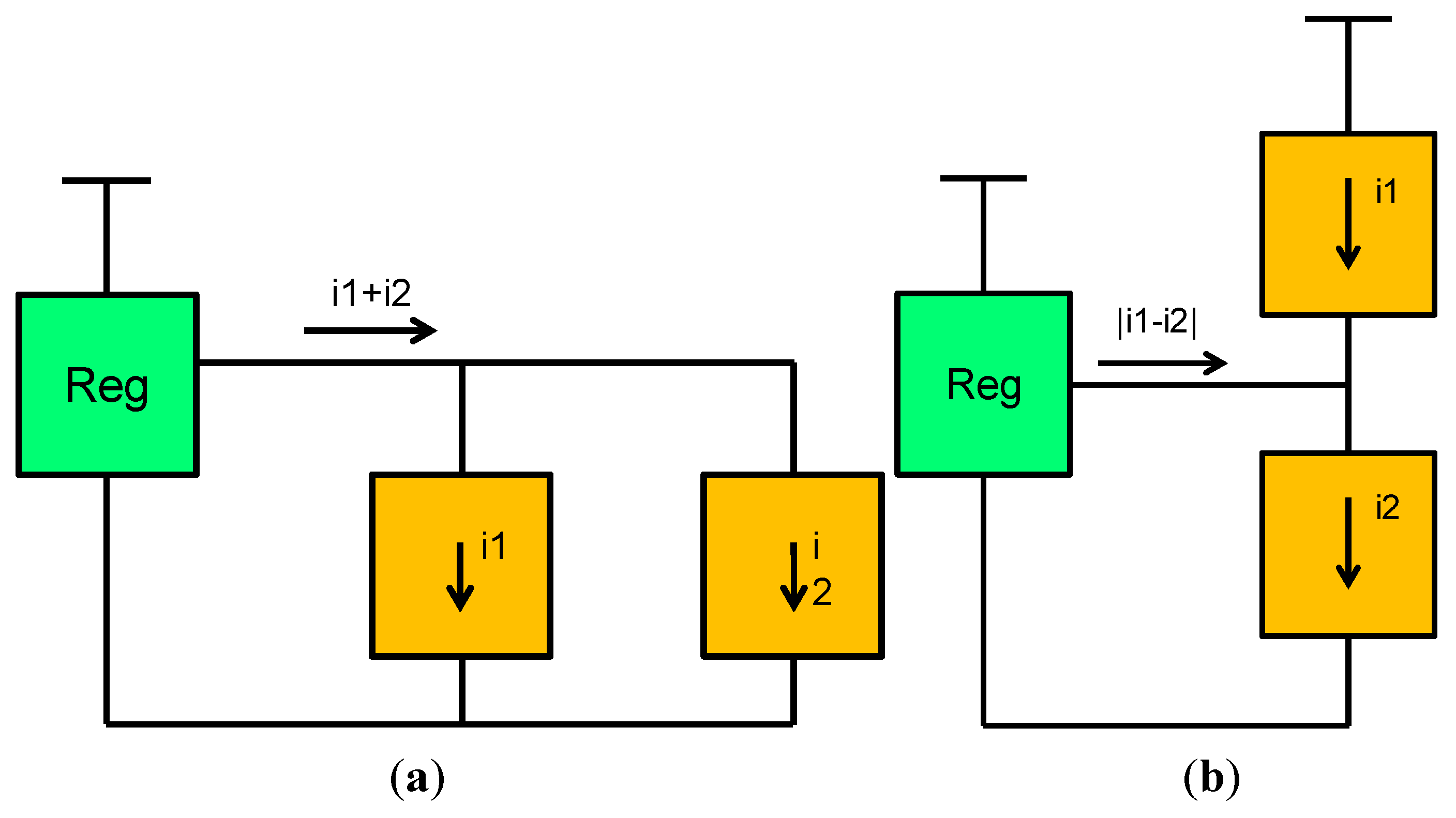
a) Implicit DC-DC down conversion through voltage stacking [
7]; (
b) Implicit voltage conversion for Resistive/CMOS load.
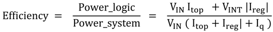
The power efficiency of this technique depends on the mismatch between the stacked domains, which in turn depends on the activity of the circuits, the evaluation node capacitance and the voltage swing in the domains. The efficiency is given by:
where |I
reg| is the difference between the top and bottom stack and I
q is the quiescent current of the regulator [
7]. Different works in the literature have handled this imbalance in different ways. In [
7], charge balance was maintained between the domains through active regulation of the intermediate node using a push-pull linear regulator. However if the top core has larger current requirements than the bottom core, then the closed-loop regulator will force the excess current to ground, thus wasting power. To compensate for this loss, granules were shifted between the domains using switching logic—this came with a power and area overhead needed for the switching logic. In [
8], a shunt regulator was used, and, to balance the different domains, software scheduling was done to distribute the workload at runtime. In our own work, we recycled the imbalance current among the stacked domains using an explicit regulator to improve the efficiency of this technique and maintain the output node within a certain tolerance limit [
9]. By using a SC regulator, the achievable efficiency can be more than LDO. This idea is an extension of our work on GALS-based stacked cores which allow the intermediate node to implicitly track the workload of the different cores [
5].
2.2. Positive/Negative Regulation
In order to recycle the current imbalance between two voltage-stacked cores, current needs to be either
sourced or
sunk from the regulator, depending on which core consumes more current. When the bottom core consumes more, current needs to be sourced (
positive regulation) which is similar to the conventional case (
Figure 2a). However, when the top core consumes more, current needs to be
sunk and we call this
negative regulation (
Figure 2b). To achieve this unique feature, we use a modified version of a conventional switched capacitor circuit [
4]. The design is implemented with eight switches and two capacitors (
Figure 3a). Unlike the case of a conventional push-pull design, with such an SC solution the
sunk current is fed back to the top core, thus reducing power waste. The two fly-capacitors change roles periodically, providing the
source/sink of charge.
Figure 2.
(a) Positive Regulation (Similar to conventional regulator, sourcing ILoad); (b) Negative Regulation (Regulator absorbs current, sinking ILoad).
Figure 2.
(a) Positive Regulation (Similar to conventional regulator, sourcing ILoad); (b) Negative Regulation (Regulator absorbs current, sinking ILoad).
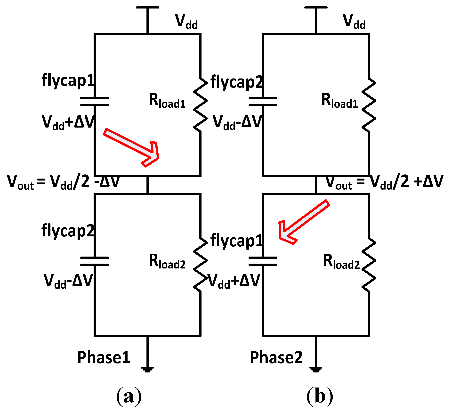
Figure 3.
(a) Illustrates the push-pull switched capacitor designed to assist voltage stacking; (b) Fly-capacitors are swapped over the phases to regulate the imbalance between the stacks. Arrows indicates the direction from which charges are flowing to and from Vout.
Figure 3.
(a) Illustrates the push-pull switched capacitor designed to assist voltage stacking; (b) Fly-capacitors are swapped over the phases to regulate the imbalance between the stacks. Arrows indicates the direction from which charges are flowing to and from Vout.
To understand how the 2:1 SC circuit works, consider an example of a slightly imbalanced workload with a supply voltage of V
dd, where the current offset pushes V
out to droop below 1/2 V
dd by ∆V (
Figure 3b). In the first phase, as the voltage droops down at the load, flyCap1 begins charging to ∆V voltage above 1/2 V
dd, while the voltage on flyCap2 falls below 1/2 V
dd by ∆V. In the second phase, through the on-chip switches, flyCap1 and flyCap2 swap places. Since flyCap1 was charged to a higher voltage, it redirects this charge back onto the V
out node. This redirection of charge helps pull the load voltage ∆V above 1/2 V
dd. This ripple (2∆V) is a manifest of the capacitor charging/discharging, and the faster the switching frequency, the lower the ripple.
2.4. Power Loss Optimization for Switched Capacitor Circuit
As explained in [
10], merely optimizing for the most energy efficient design can be misleading or impractical. Ideally the optimization should try to achieve the minimum energy point subject to some design constraint, for example by using the concept of
hardware intensity [
10]. In our work, we considered a design methodology to maximize the achievable efficiency by tuning different
sensitivity knobs for a given area constraint [
11,
12].
In [
9] we briefly discussed the design rules for this regulator. For a given current imbalance, while the fly-capacitor size determines the
amount of charge that can be delivered, the switching frequency sets the
output ripple. Taking maximum ripple as a design constraint, we chose the capacitor size and switch width as the two tuning knobs. As pointed out in [
11], an energy efficient design is achieved when the costs (sensitivity ratios) of tuning the knobs are balanced. Each of the points on the energy-area design space represents percent power loss per percent area for an energy-efficient regulator design. In order to understand the design space, we developed analytical expressions (sensitivities) for all the tuning variables [
12].
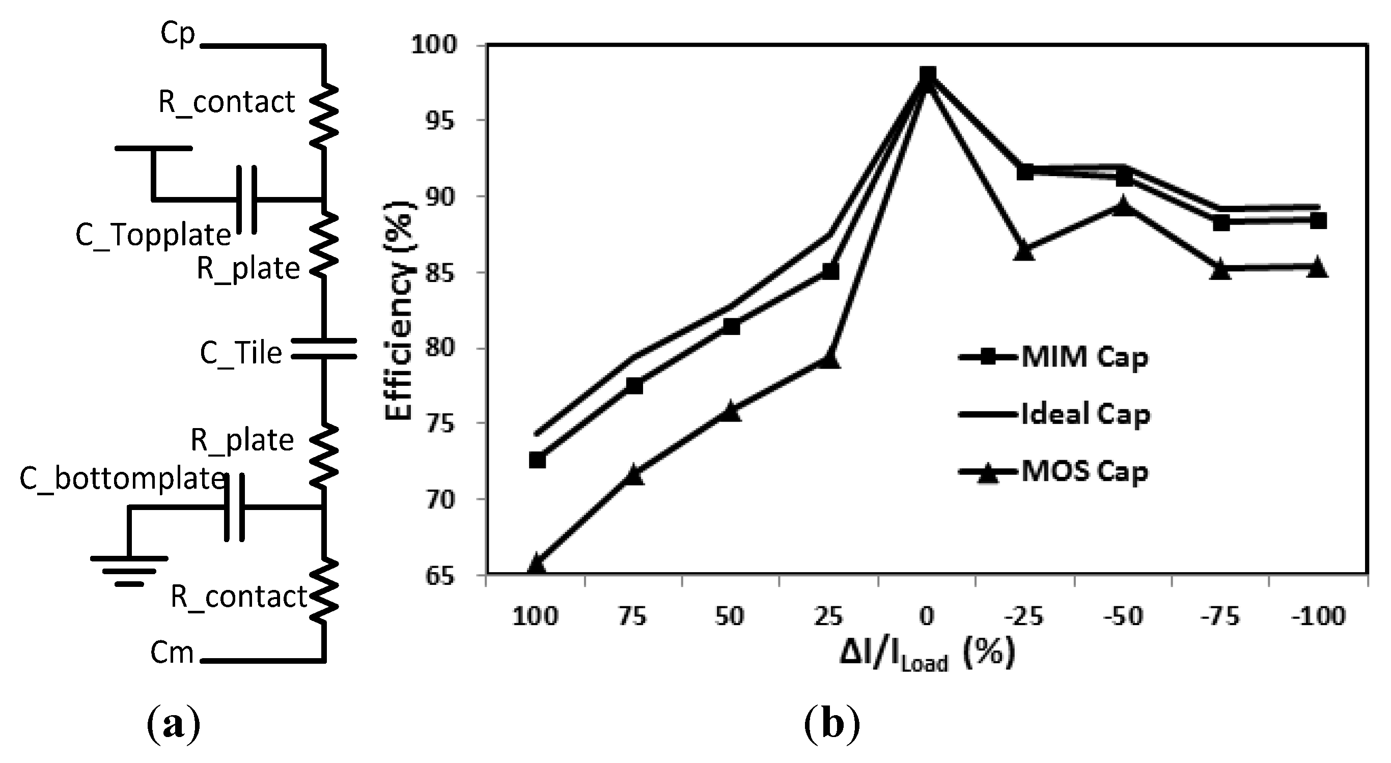
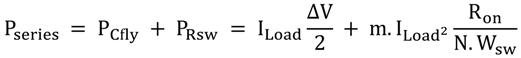
Switched capacitor circuit power loss can be categorized into two kinds, the series loss and the shunt loss [
4]. Series loss consists of the intrinsic switched capacitor loss and the conductance loss of the switches:
where R
on is the switch resistance density (ῼ.m); W
sw is the size of each of the switches (we took all the switches to be equal sized); N the number of switches and m is a constant determined by the switched capacitor topology [
4].
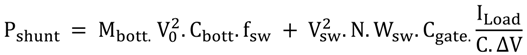
The additional shunt losses arise from switching the parasitic capacitance of the fly-capacitors and the power switches:
where M
bott is a constant depending on SC topology; V
o and V
sw are the bottom plate-capacitor (plate-cap) and gate voltage swings; C refers to the fly-capacitor; C
gate refers to the gate oxide capacitance (gate-cap) of the switches and ∆V is the voltage droop.
The bottom plate-cap loss scales with only frequency while the gate-cap loss scales with both frequency and switch width. At higher load-currents the latter starts dominating, hence we neglected the bottom plate loss in our analysis. Also by using metal-insulator-metal (MIM) or trench-capacitors for the fly-capacitors, the bottom-plate loss can be minimized further. Thus total loss in switched capacitor regulator is given by:
2.5. Sensitivity Analysis
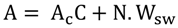
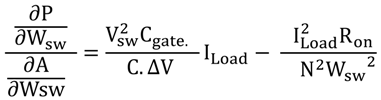
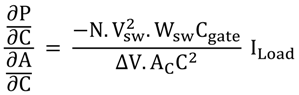
As mentioned before, we selected fly-capacitor and switch width as the two tuning variables for studying the power loss vs. area tradeoff-sensitivity analysis of the cost metrics with respect to the tuning variables and equalizing the cost across the design space provides us with optimum design points. We chose the power loss and area consumed by the switched capacitor circuit as the cost metrics:
where A is the total area and A
c is the area per unit capacitance—this value will depend on the capacitor technology. In our model we used the value assuming MIM cap density of 3 nF/mm
2. In [
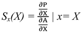
11] the sensitivity ratio for knob X is defined as:
where S
x represents the amount of energy that can be traded-off for area by tuning variable X. The sensitivity of power loss to area due to switch width and fly capacitor are given by:
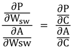
For optimizing the design in the energy/area design space, the costs across the tuning variables should be equal [
11]:
This means that at optimal design points, any marginal gain in energy will result in the same percentage amount of loss in area. The values of R
on and C
gate are fixed, depending on the technology node, while fly-capacitor values are chosen in accordance with the maximum allowable droop ∆V and I
Load max. In this topology, I
Load max refers to the worst-case current imbalance between the domains. Plugging-in the values and solving for W
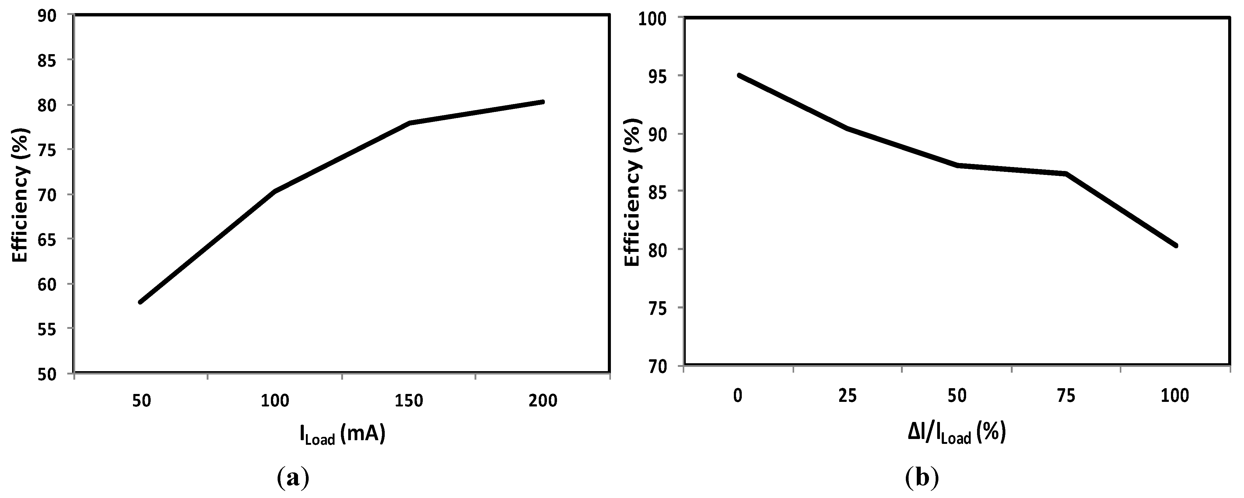
sw provides the optimum switch width for a given capacitor size at the minimum energy point. Thus this global optimization process can allow us to look at the entire design space while balancing out the different tuning variables depending on the weight of their individual cost. To verify our claim, we did a Monte Carlo simulation selecting a large number of arbitrary capacitor values and switch widths and plotting them against our result based on sensitivity optimization. As can be seen in
Figure 5, our method indeed yields the lowest points in the design space, also known as the Pareto curve. Based on the above optimization, for a given fly-capacitor size, allowable droop, and maximum I
Load, we can find the optimum switch widths. In
Figure 6, we plugged-in this optimal value of switch width and performed efficiency analysis for different load currents. Unlike for a conventional regulator, the optimization of a voltage-stacked regulator will depend not only on the I
Load but also on the difference of current between the domains [
6]. In order to have a fair comparison, we kept one of the stacked loads at 200 mA while varied the other load from 0–200 mA. We have plotted this ratio of current imbalance to chip current consumption (∆I/I
Load) along the x-axis in
Figure 6b. As can be seen from the plots, stacked regulation can yield higher efficiency, and since the bulk of the current comes from the off-chip supply, the switch widths and fly-capacitor area can be reduced to improve the power density of the circuit. Stacked regulation achieves 81%–95% efficiency (depending on imbalance between stacked domains) compared to 81% for non-stacked load of 200 mA for 1.2 V–0.6 V down conversion. Thus it is fair to say, even in the worst case, stacked regulation is comparable to the best case in conventional SC regulation [
9].
2.6. Open-Loop versus Closed-Loop
In SC circuits, regulation is performed by modulating the output resistance of the converter in response to changes in load current [
13]. The output of a SC converter is given by:
Figure 5.
Monte Carlo Analysis of power optimization. Zoomed in view (right) shows that our sensitivity-based optimization gives the lowest points on the curve.
Figure 5.
Monte Carlo Analysis of power optimization. Zoomed in view (right) shows that our sensitivity-based optimization gives the lowest points on the curve.
Figure 6.
(a) Efficiency with varying conventional load (left); (b) Stacked load (right) with max ILoad = 200 mA. The X-axis indicates relative imbalance (%) between the domains.
Figure 6.
(a) Efficiency with varying conventional load (left); (b) Stacked load (right) with max ILoad = 200 mA. The X-axis indicates relative imbalance (%) between the domains.
where n is the conversion ratio; f
sw the switching frequency; D
i the duty cycle of switching and G
i the conductance of the switches. Each of these variables can be used to control regulation. The conversion ratio (n) is fixed by the number of layers (cores) stacked. One of the main drawbacks of varying Di or Gi of the switches at constant frequency is reduced efficiency at lighter load. However, keeping duty cycle fixed at 50% and by modulating switching frequency with load current, higher efficiency can be achieved, especially at lighter load [
4]. The downside of this is the high output voltage ripple as charge transfer is impulsive with slow switching limit of frequency [
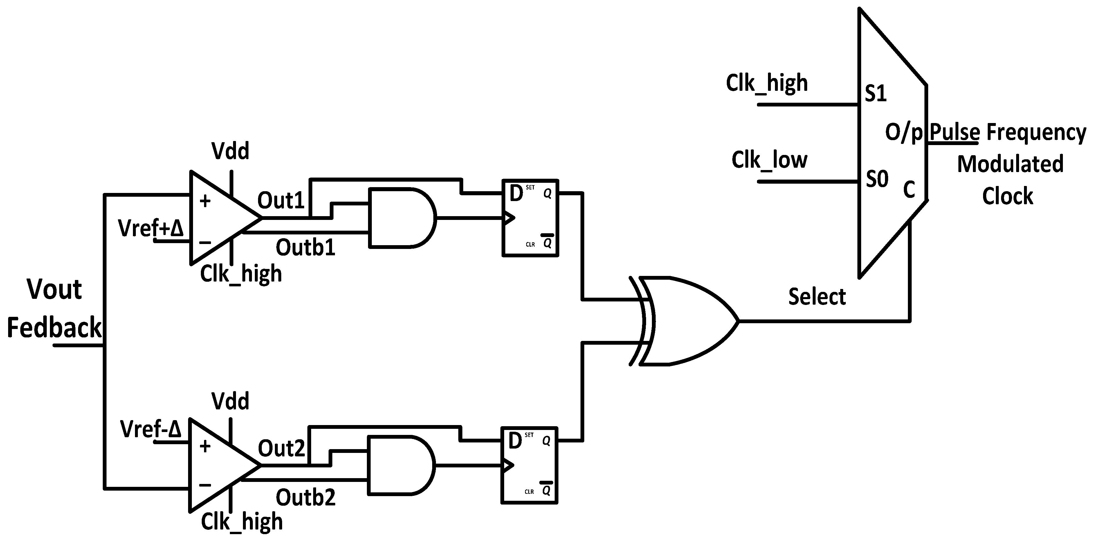
14]. Hybrid regulation, with two or three control variables together, will bring the highest efficiency, however complicated the control circuitry. In our work, we used modulation of switching frequency as the controlling variable with additional interleaving mechanism to reduce the output ripple. The traditional control method for a SC converter may include a linear feedback loop to control the switching frequency in terms of the output voltage. However obtaining stability and good transient response over varying load conditions using such a control method is difficult. A nonlinear control can provide superior results; hence we have used a hysteretic feedback scheme with lower and upper bounds to control the regulation (
Figure 7) [
15]. However our control circuit is different from traditional hysteretic control and the difference comes from the stacked loads as opposed to conventional parallel loads. As explained above, current needs to be either sourced or sunk in this type of load. Consequently the output can go both high and low depending on the current mismatch between the layers, hence higher switching frequency (Clk_high) is needed whenever either of the boundaries is crossed by output voltage while low frequency (Clk_low) can regulate the in-between state.
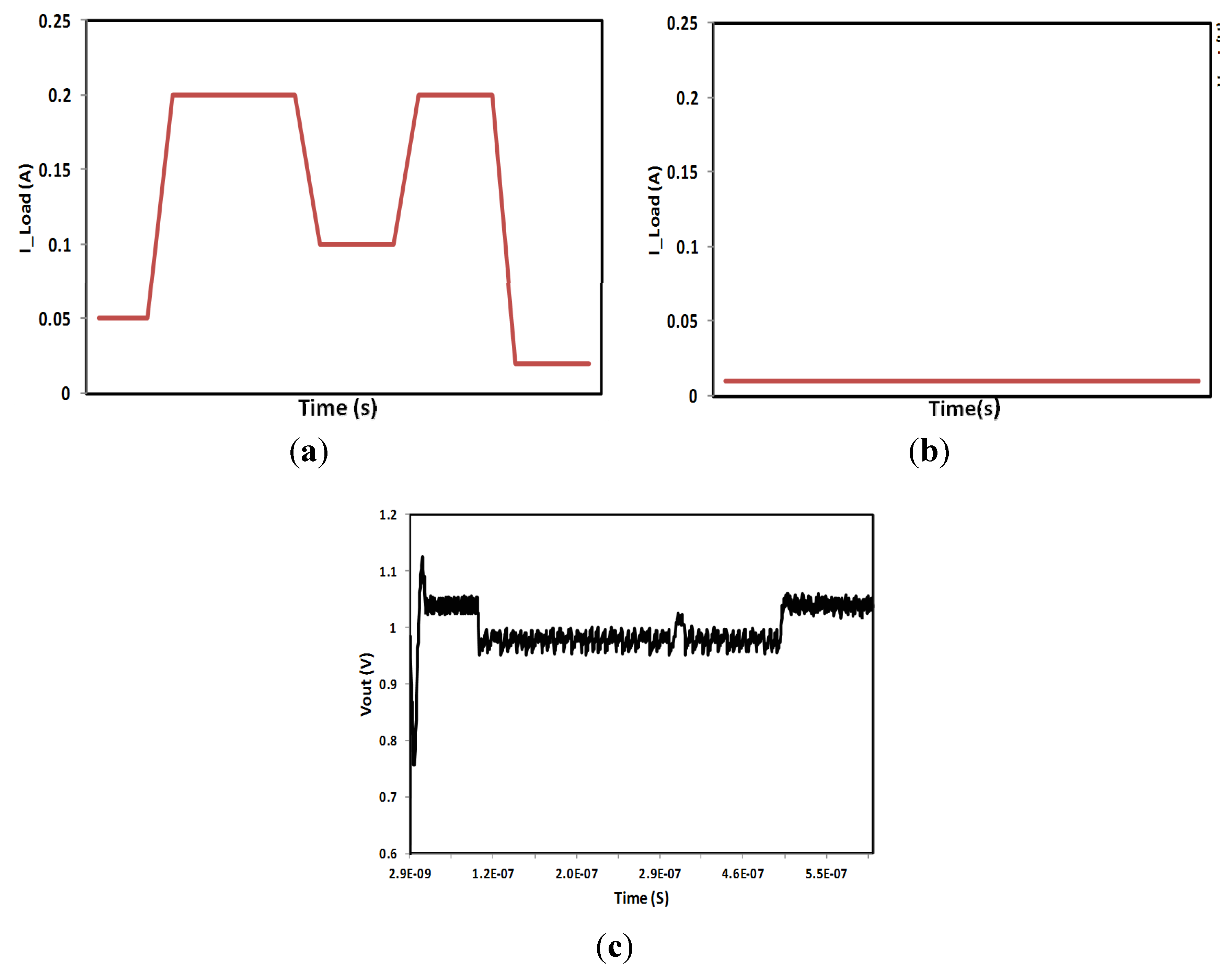
Table 1 explains the states.
Figure 7.
Dual-boundary hysteretic feedback control scheme for stacked load. Output clock is pulsed between high and low frequency depending on comparator detected trigger signal.
Figure 7.
Dual-boundary hysteretic feedback control scheme for stacked load. Output clock is pulsed between high and low frequency depending on comparator detected trigger signal.
Table 1.
Different states for the feedback circuit to regulate Vout.
Table 1.
Different states for the feedback circuit to regulate Vout.
| State of O/P | Out1 | Out2 | Select | O/P Clock |
|---|
| Vout > Vref + ∆ | Toggle | Low | 1 | Clk_high |
| Vref - ∆ < Vout < Vref + ∆ | Low | Low | 0 | Clk_low |
| Vout < Vref - ∆ | Low | Toggle | 1 | Clk_high |
The feedback circuit consists of two comparators (along with latches, XOR gate and mux) that detect when the output voltage crosses the control boundary. By adding an edge-triggered latch we make sure that only rising edges are associated with a charge transfer [
15]. If there were no latches, then the falling edge, which appears because of the clocked comparator and not as a trigger for boundary crossing, will cause an unwanted charge transfer. In order to account for comparator response time, we generated the clock to the latches out of the comparator itself—consequently comparator delay implicitly tracks across all PVT corners. Depending on the “Select” signal which triggers the output mux, low or high clock frequency is applied to the switches. A latch-based voltage sense amplifier was used to reduce power consumption [
16]. The dual-comparator and logic gate controlled feedback circuit power consumption are critical, especially for low power operation. For 2 V–1 V stacked conversion for a load current of 200 mA with the comparator running at 1 GHz, feedback circuit power consumption is 1.2 mW. However this can be scaled down depending on the operational frequency of the load. For the low power (1.2 V–0.6 V, 10 mA) conversion, feedback power scales down to 0.2 mW.
This feedback circuit was used with the SC converter and we have done extensive simulations for 2:1 DC-DC conversion using both parallel loads and stacked loads. Near threshold circuits are typically operated 200 mV above their threshold value [
17]. Hence here we considered 0.6 V as NTC V
out to be delivered. Conversion efficiency for both low power (0.5 mW–10 mW, 1.2 V–0.6 V) and high power (10 mW–400 mW, 2 V–1 V) loads have been shown for comparison.
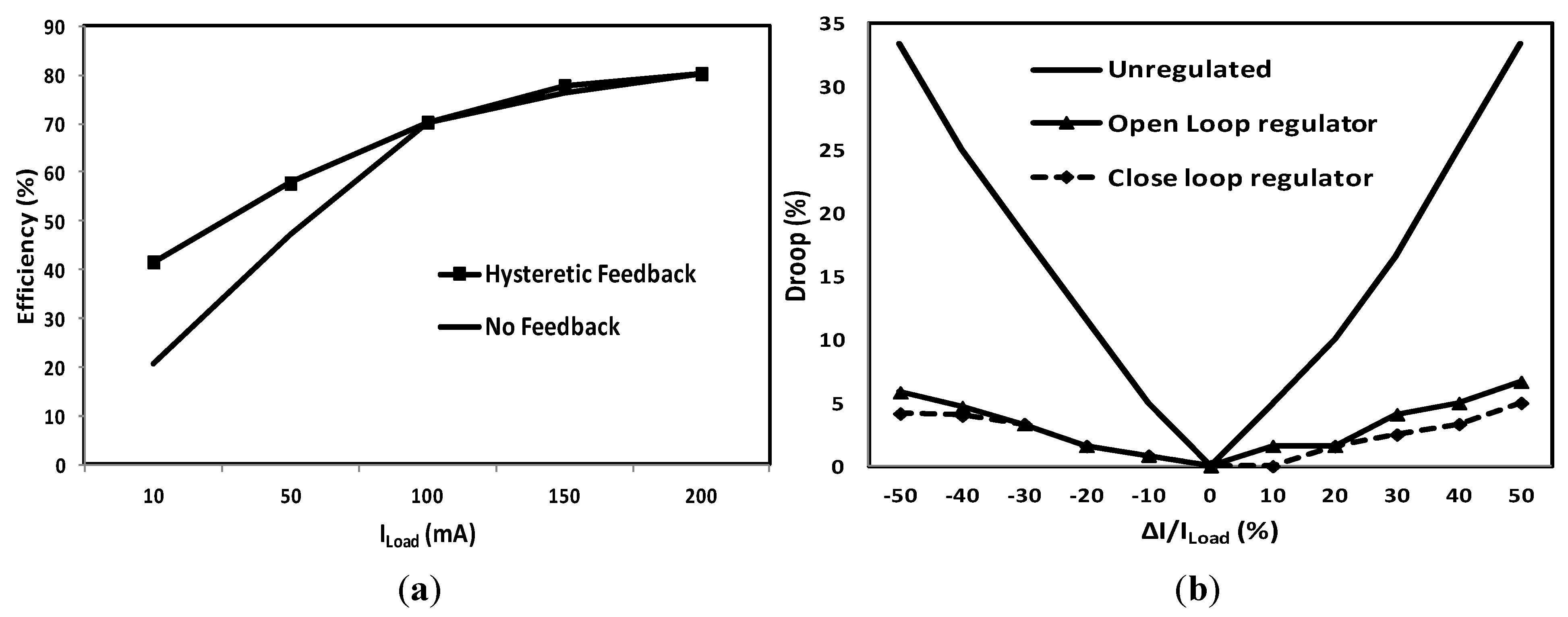
Figure 8.
(a) Feedback SC circuit applied to conventional load; (b) Comparisons between unregulated, open-loop and closed-loop stacked loads.
Figure 8.
(a) Feedback SC circuit applied to conventional load; (b) Comparisons between unregulated, open-loop and closed-loop stacked loads.
As
Figure 8a shows, the feedback circuit has considerable impact on efficiency for conventional load, especially at lower current. However stacked load has unique characteristics which are explained below with the help of
Figure 1a [
9].
In
Section 2.1 we discussed how the nature of the load can affect voltage stacked DC-DC conversion. Here we discuss how the voltage headroom in each of the stacked cores is going to change with load or activity variation. CMOS load has been considered here, representing the core (
Figure 1a).
By charge conservation:
Current consumption of the two cores is given by:
where α
top and α
bottom are the top and bottom core activity factors; F
c is the core frequency and V
mid is the implicit voltage generated by stacking two cores.
However, if α
top > α
bottom, V
2 > V
1; α
top < α
bottom, V
1 > V
2. This means that the inherent feedback of voltage stacking forces the voltage headroom to be lower for the core that demands
higher current, thus acting against the idea of DVFS (that when computing demands are
lower the voltage should be reduced). Therefore, this internal voltage buildup in voltage stacking can not only add noise to the stacked cores, but also oppose DVFS. This is shown in
Figure 8b. The more the imbalance, the more the self-regulation of the system will force the V
mid node to go in the opposite direction as seen from the unregulated stacked mid rail. Thus for voltage stacking to work, we need to compensate for this natural feedback tendency and the push-pull scheme is therefore essential for maintaining the charge imbalance within bounds.
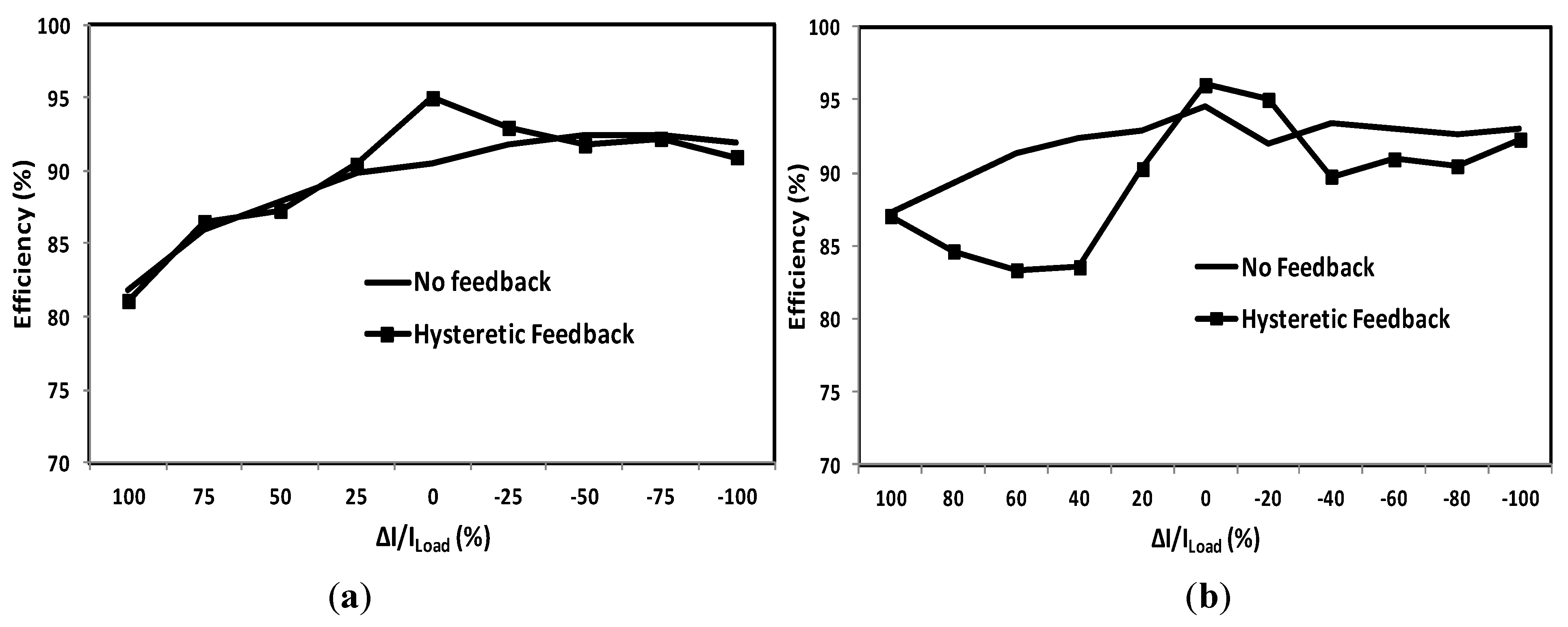
However whether adding a feedback loop over the SC converter can bring any benefits or not, is what we try to show in
Figure 9a,b. As shown in some of the earlier plots, to demonstrate effectiveness of voltage stacking, efficiency needs to be plotted against the ratio of load current to load imbalance. Thus midpoint on the x-axis for both the plots indicates when the loads are perfectly balanced. Ideally the SC does not need to regulate at that point and it can lower its switching frequency to minimal value to improve energy efficiency. This is shown in
Figure 9a,b where the feedback controller reduces the switching frequency around the balanced load condition (midpoint region ofx-axis) and increases the efficiency as compared to the open loop regulator. However when the loads are not in balance, the performance of the closed loop regulator is in fact worse compared to the open loop one for low power loads (
Figure 9b). This is because for low power (NTC) stacked loads, the feedback circuit overhead reduces the efficiency. At an imbalance of 50%, closed-loop SC converter suffers an efficiency loss of 10.8% over an open-loop SC converter. Thus for low power DC-DC conversion, voltage stacking can provide an attractive alternative technique and by removing the additional losses in the feedback circuitry, the efficiency can be improved further [
9]. However, for closely matched high power loads, hysteretic feedback can still provide higher efficiency as shown in
Figure 9a.
Figure 9.
(a) Comparison of open-loop/close-loop SC circuit for high power: 10 mW-400 mW, 2 V–1 V; (b) Low power: 0.5 mW–10 mW, 1.2 V–0.6 V.
Figure 9.
(a) Comparison of open-loop/close-loop SC circuit for high power: 10 mW-400 mW, 2 V–1 V; (b) Low power: 0.5 mW–10 mW, 1.2 V–0.6 V.

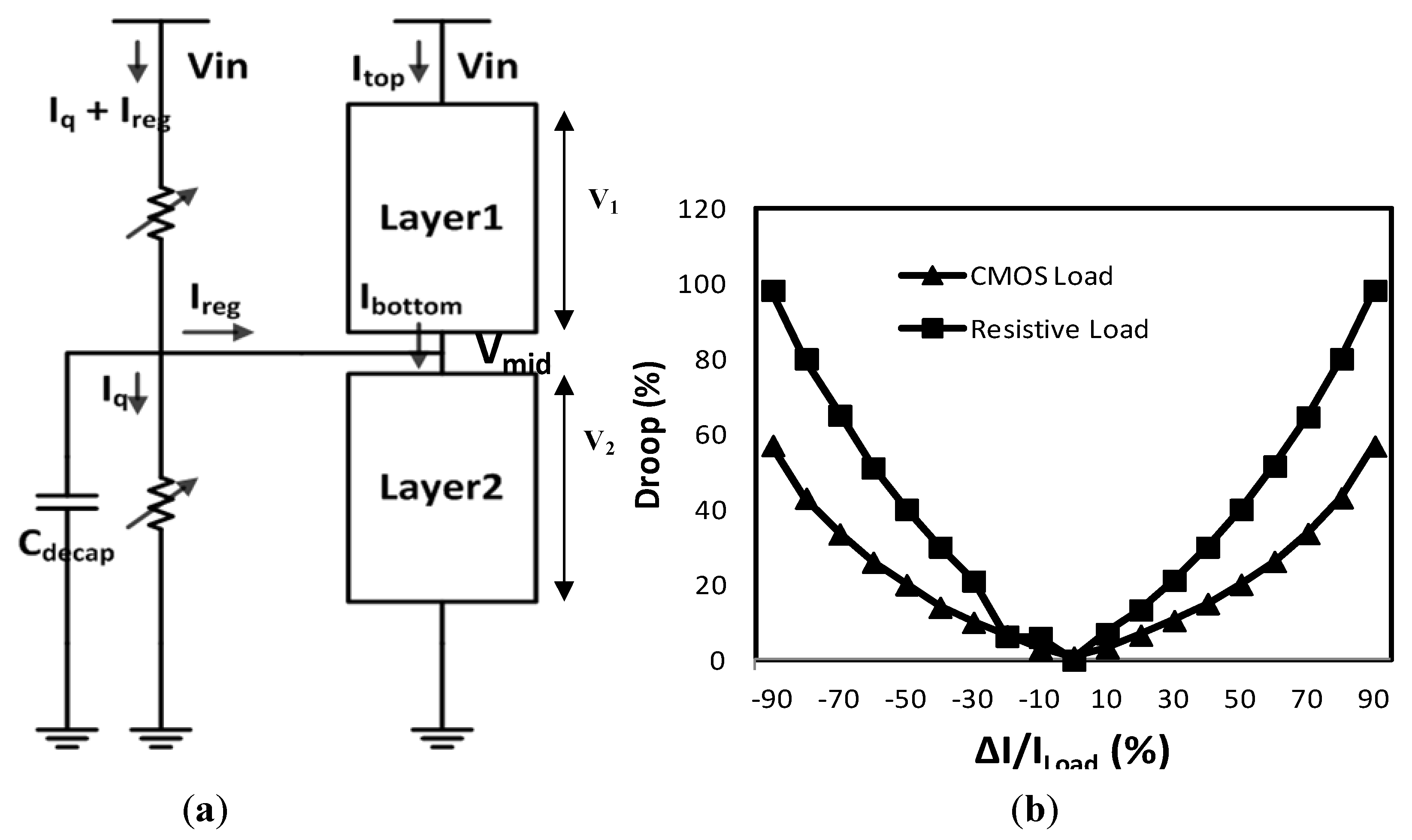
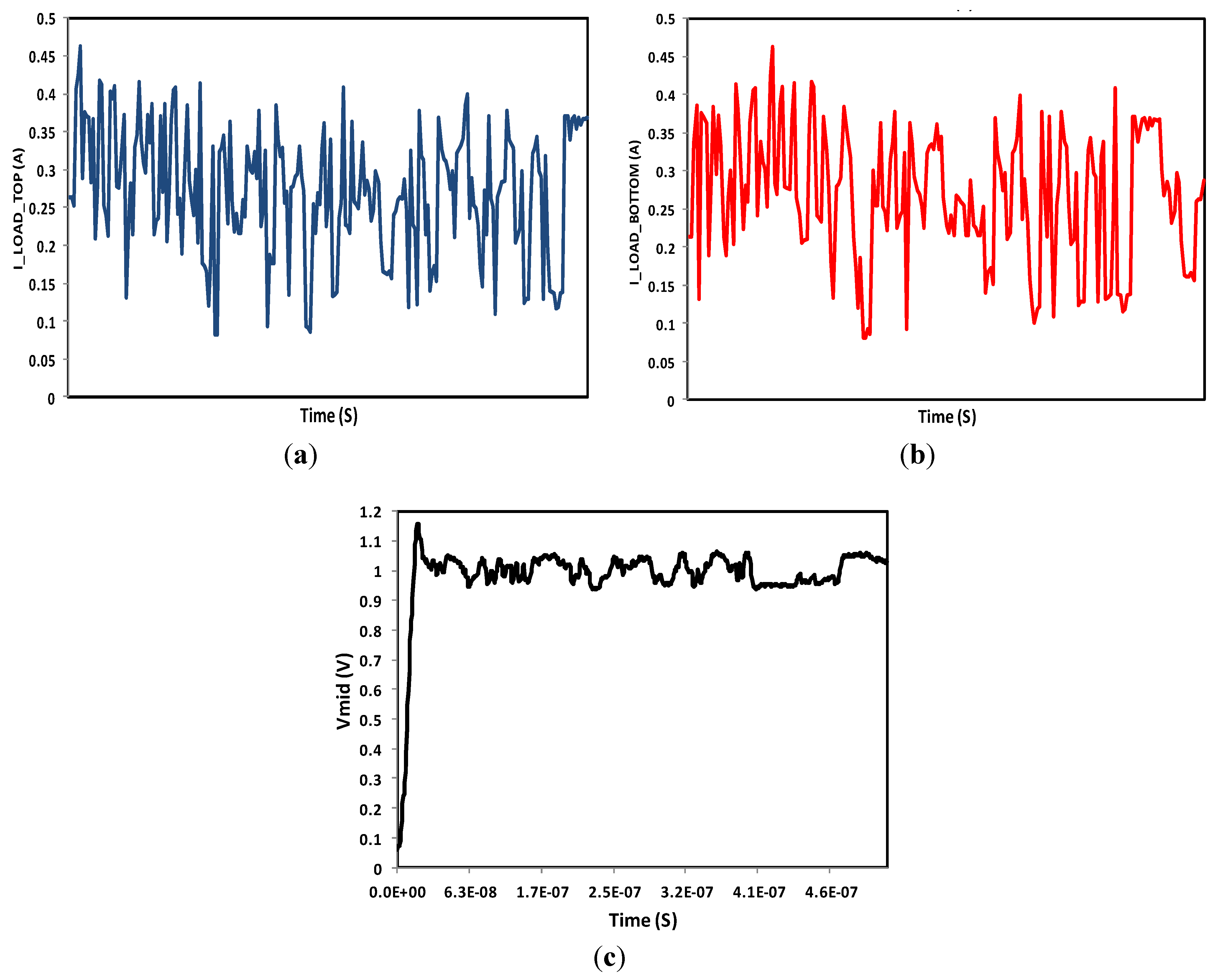
 while VResistive α IResisitve. Therefore, load current imbalance will cause a larger variation in resistive load than CMOS load. This quadratic versus linear dependency between voltage and current is also evident from Figure 1b where mid-voltage droop due to resistive load variation is larger than due to CMOS load variation.
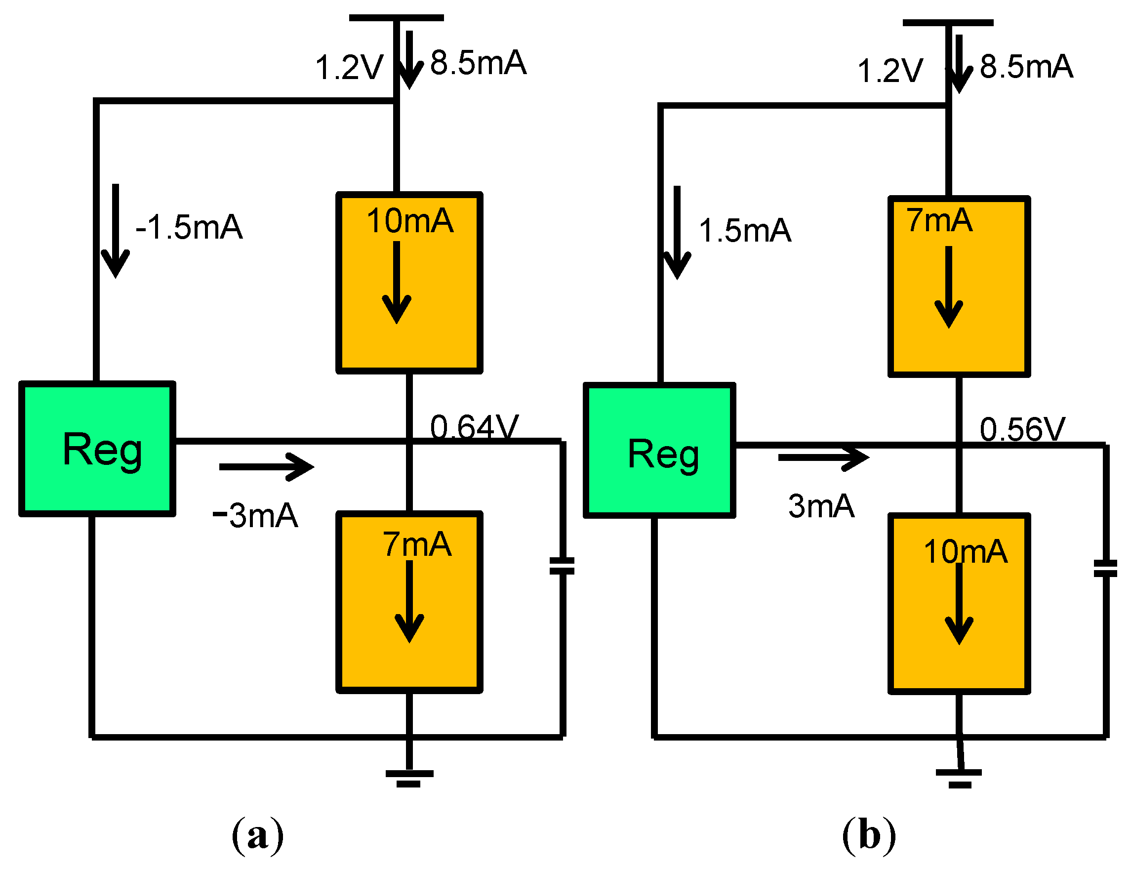


