Article

A Cross-Layer Framework for Designing and Optimizing Deeply-Scaled FinFET-Based Cache Memories †

Department of Electrical Engineering, University of Southern California, Los Angeles, CA 90089,USA
*
Author to whom correspondence should be addressed.
This paper is an extended version of our paper published in The IEEE S3S Conference 2014, entitled “A Cross-Layer Design Framework and Comparative Analysis of SRAM Cells and Cache Memories using 7 nm FinFET Devices”.
J. Low Power Electron. Appl. 2015, 5(3), 165-182; https://doi.org/10.3390/jlpea5030165
Submission received: 3 March 2015 / Revised: 23 June 2015 / Accepted: 28 July 2015 / Published: 11 August 2015
(This article belongs to the Special Issue Selected Papers from IEEE S3S Conference 2014)

Abstract

:
This paper presents a cross-layer framework in order to design and optimize energy-efficient cache memories made of deeply-scaled FinFET devices. The proposed design framework spans device, circuit and architecture levels and considers both super- and near-threshold modes of operation. Initially, at the device-level, seven FinFET devices on a 7-nm process technology are designed in which only one geometry-related parameter (e.g., fin width, gate length, gate underlap) is changed per device. Next, at the circuit-level, standard 6T and 8T SRAM cells made of these 7-nm FinFET devices are characterized and compared in terms of static noise margin, access latency, leakage power consumption, etc. Finally, cache memories with all different combinations of devices and SRAM cells are evaluated at the architecture-level using a modified version of the CACTI tool with FinFET support and other considerations for deeply-scaled technologies. Using this design framework, it is observed that L1 cache memory made of longer channel FinFET devices operating at the near-threshold regime achieves the minimum energy operation point.

1. Introduction

FinFET devices are currently viewed as the technology-of-choice beyond the 10-nm regime [1]. This is mainly due to the improved (three-dimensional) gate control over the channel and less control by source and drain terminals, which subsequently makes FinFETs more immune to short channel effects (SCE) [2]. Moreover, the absence of channel doping in FinFETs eliminates the random dopant fluctuation, resulting in higher immunity to process-induced variations and soft errors [3,4]. Additionally, the minimum energy point and the minimum energy-delay product point of FinFET circuits occur at supply voltage levels lower than that of planar CMOS counterparts [5], which enables more aggressive voltage scalability in FinFET-based circuit designs.
On the other hand, SRAM cache memories, because of occupying a large portion of the chip area [6] and also due to relatively low activity factors (i.e., long idle periods), consume a large portion of the overall chip power consumption [7]. Furthermore, by moving toward deeply-scaled technology nodes, extremely small geometries along with reduced V d d levels (which narrow the difference between supply and threshold voltages) will exacerbate the sensitivity of circuits to process variations. Unfortunately, this situation becomes worse in cache designs, where minimum-size transistors are preferred to maintain high memory densities. Accordingly, memory systems are considered as the major bottleneck of the V d d scaling [8]. In order to resolve this issue, FinFET-based SRAM cells have emerged as a solution to a more robust and energy-efficient memory design [9]. However, the effect of each FinFET geometry on characteristics of SRAM cells and, more importantly, on characteristics of cache memories (system-level properties) has not been investigated.
This paper thus adopts a cross-layer design framework in order to study the effect of deeply-scaled (7 nm) FinFET devices on cache memories. The proposed design framework, as shown in Figure 1, spans device, circuit and architecture levels as follows.
Figure 1. The proposed cross-layer design framework for characterizing SRAM cells and cache memories manufactured with deeply-scaled FinFET devices.
Jlpea 05 00165 g001
At the device level (Section 2), various FinFET devices for a 7-nm process, including a baseline device and six other devices, where in each device, only one geometry is changed, are designed using Synopsys TCAD tools [10]. Verilog-A models are then extracted from the device simulator, which are used at the circuit level (Section 3) in order to perform fast SPICE-based simulations, such as deriving characteristics of SRAM cells. Finally, at the architecture level (Section 4), the overall characteristics of an on-chip cache memory is assessed using a modified version of the CACTI tool with FinFET support and other considerations for deeply-scaled technologies.
Using this cross-layer design framework, the conventional eight transistor (8T) SRAM cell [15] using a longer channel FinFET device is suggested as the choice of memory cell for the proposed 7-nmFinFET process.

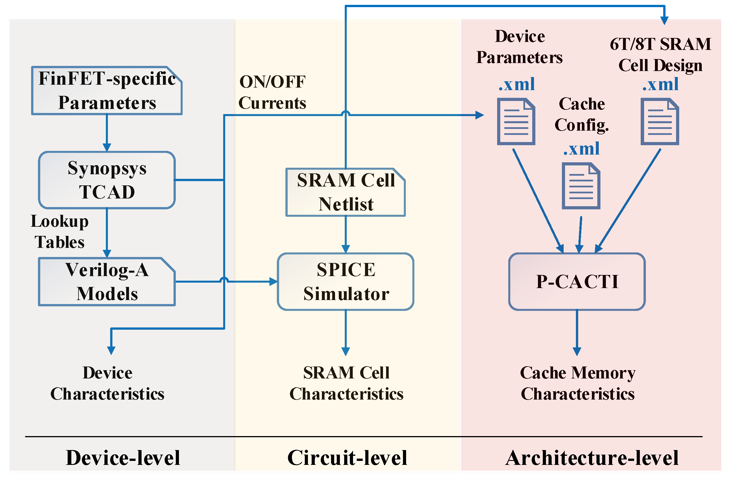
2. Device-Level Design and Optimization
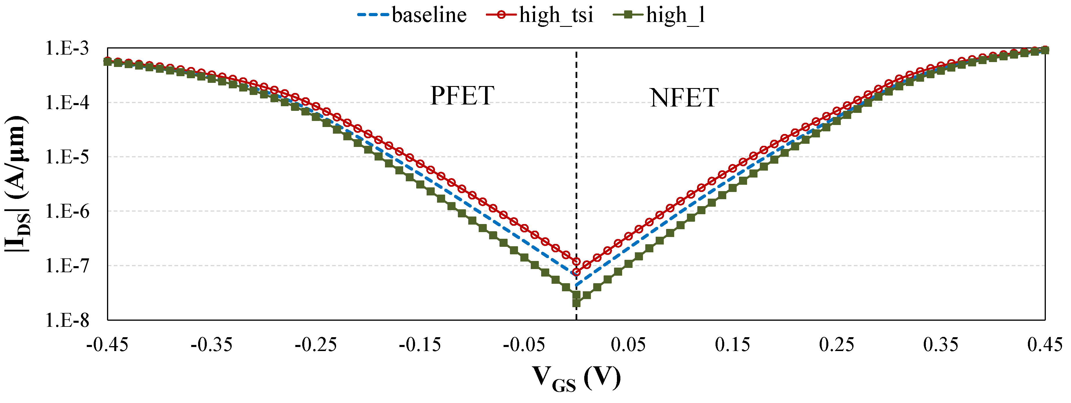
In this section, our 7-nm FinFET devices are introduced. We then compare their ON current, OFF current and ON/OFF current ratio values.

2.1. FinFET Devices

The main component that distinguishes the FinFET process from the planar CMOS counterpart is the fin, which provides the channel for conducting current when the device is switched on. This vertical fin is surrounded on three sides by the gate, and hence, a more efficient control over the channel is established, which in turn helps to reduce SCE. Key geometric parameters of a FinFET device include the fin height ( H F I N ), the fin width, also known as the silicon thickness ( T S I ), the gate or fin length ( L F I N ) and the gate underlap ( u l ), which is the distance between the edge of the gate strip and source (or drain) terminal. This gate underlap is introduced to mitigate the direct source-to-drain tunneling (DSDT) current [11], which subsequently diminishes source and drain controls over the channel, thereby further improving the immunity of FinFET devices to SCE.
The effective channel width of a single-fin FinFET is equal to W m i n = 2 × H F I N + T S I , which is the minimum achievable channel width in FinFETs. However, in order to increase the width (strength) of a FinFET device, more fins in parallel are added. As an example, the structure and layout of a FinFET with two fins are illustrated in Figure 2a,b, respectively. The critical geometry in these figures is the fin pitch, P F I N , which is defined as the minimum spacing between the center of two adjacent parallel fins. Hence, the layout area of a FinFET device is proportional to: (i) the number of fins; and (ii) the value of P F I N , which is dictated by the underlying FinFET technology.
7 nm FinFET Devices: In this paper, we intend to investigate the power and performance behaviors of advanced FinFET devices on memory designs. Accordingly, FinFET devices with an actual gate length of 7 nm are adopted. However, since no industrial data for such deeply-scaled FinFET devices are publicly available, our 7-nm FinFET devices [12] are modeled (cf. Figure 2c) and simulated using Synopsys Sentaurus Device [10]. Table 1 reports the design parameters of the baseline (standard) 7-nm FinFET device. More precisely, the gate length of the baseline device is 7 nm, with 1.5-nm gate underlap on each side, resulting in a channel length of 10 nm. Furthermore, the supply voltage, V d d , is 0.45 V for super-threshold, and 0.3 V for near-threshold operations.
In addition to the baseline device, we developed six other variations of 7-nm FinFET devices with only one geometry changed per device. In order to avoid significant changes in the layout structure and manufacturing steps, we selected 10%–15% variation from the nominal value of L F I N , T S I and t o x [13]. However, the value of u l has been aggressively (50%) increased in order to better study the impact of the gate underlap on FinFET characteristics. Design parameters of other devices are reported in Table 2. | I D S | vs. the V G S characteristics of baseline, high_tsi, and high_l FinFET devices are shown in Figure 3. The threshold voltage values, V t , of our FinFET devices are between 0.2 V and 0.25 V.
Figure 2. (a) Structure and (b) layout of a FinFET device with two fins; (c) 2D model of 7-nm FinFET devices in TCAD.
Jlpea 05 00165 g002
Figure 3. | I D S | vs. V G S characteristics of baseline, high_tsi and high_l FinFET devices.
Jlpea 05 00165 g003
Table 1. Design parameters of the baseline 7-nm FinFET device [12]. NFET and PFET denote N-type and P-type FinFET devices, respectively.
Parameter nameValueParameter nameValue
Gate length ( L F I N )7 nmGate oxide materialSiO 2 + HfO 2
Fin width ( T S I )3.5 nmSource/Drain doping1 × 10 20 cm - 3
Fin height ( H F I N )14 nmGate work function (NFET)4.4 eV
Gate oxide thickness ( t o x )1.3 nmGate work function (PFET)4.9 eV
Gate underlap ( u l )1.5 nmFin pitch ( P F I N ) 2 λ + T S I = 10.5 nm
Table 2. Design parameters of other 7-nm FinFET devices. For each device, only one geometry is changed.
DeviceParameterValueDeviceParameterValue
low_tsi T S I 3.2 nmlow_tox t o x 1.1 nm
high_tsi T S I 3.8 nmhigh_tox t o x 1.5 nm
high_ul u l 2.25 nmhigh_l L F I N 8 nm

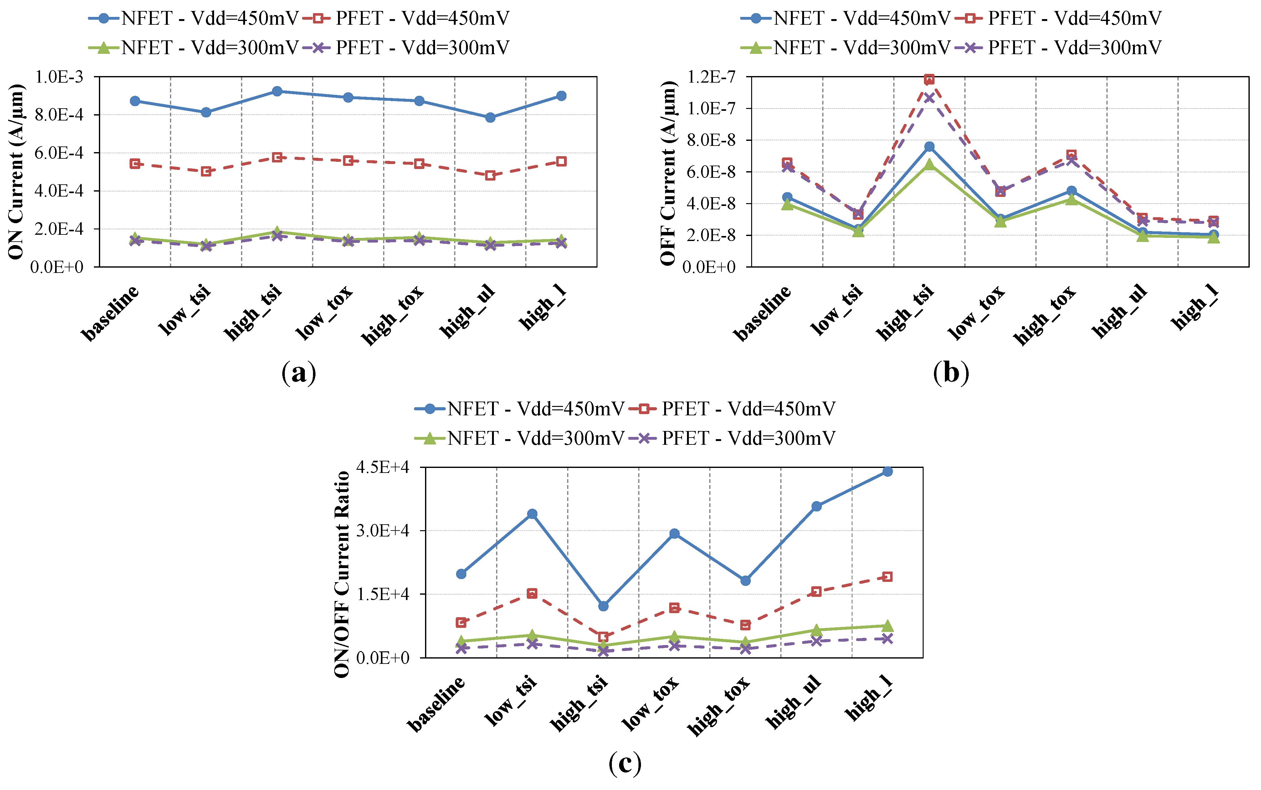
2.2. Device-Level Comparison

ON current, OFF current and ON/OFF current ratio values of 7-nm FinFET devices under super- and near-threshold operations are shown in Figure 4a–c, respectively. According to Figure 4a, the highest ON current (6% higher than that of the baseline) is achieved by the high_tsi device, which has a larger fin width (which means a larger effective channel width) compared to the baseline device, but this larger fin width also increases the leakage current, and hence, the highest OFF current (76% higher than that of the baseline) is also achieved by the high_tsi device. Based on these results, the high_tsi device has the worst ON/OFF current ratio among our FinFET devices. On the other hand, as a result of the V t roll-off effect, the lowest OFF current (2.2× lower than that of the baseline) is obtained by using the high_l device, which has a longer gate length compared to the baseline device. Further, the ON current of the high_l is 2.5% larger than that of the baseline device, and thus, the highest ON/OFF current ratio is achieved by the high_l device.
Figure 4. (a) ON currents; (b) OFF currents; and (c) ON/OFF current ratios of N- and P-type FinFET devices under super- ( V d d = 450 mV) and near-threshold ( V d d = 300 mV) regimes.
Jlpea 05 00165 g004
The V d d reduction in the near-threshold operation demonstrates a ∼6× decrease in the ON current of N-type FinFETs (NFETs), and a ∼4× decrease in the ON current of P-type FinFETs (PFETs). However, the reduction in OFF current is not so significant as indicated in Figure 4b, which is because of the negligible drain-induced barrier lowering (DIBL) effect in FinFET devices. On the other hand, the NFET over PFET ON current ratio in our FinFET devices is on average 1.6 in the super-threshold regime, but 1.1 in near-threshold operation. Accordingly, in near-threshold operation, our NFET and PFET devices have similar ON currents (strengths).

3. Circuit-Level Design and Optimization
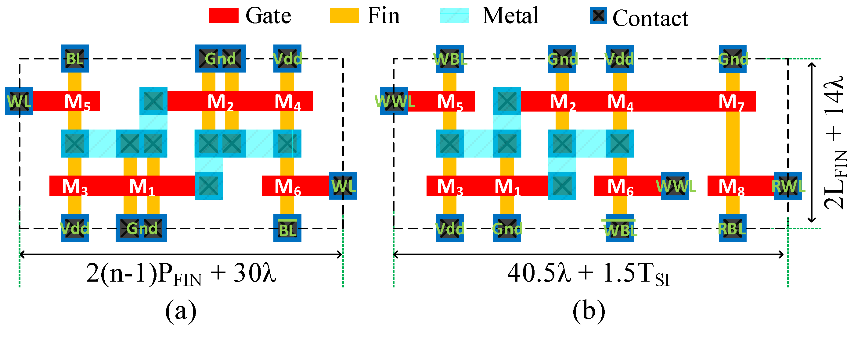
After FinFET devices have been designed using the Synopsys Sentaurus Device, a series of lookup tables is generated (because of the complex gate control in deeply-scaled FinFETs, lookup tables instead of analytical models are used to describe device characteristics). These lookup tables receive drain-source and gate-source voltages as inputs, and return the current going into each terminal, as well as the parasitic capacitances. Verilog-A models are then created, which will act as the interface between the SPICE simulator and the aforementioned lookup tables. These SPICE-compatible Verilog-A models allow us to perform fast gate- and circuit-level simulations, compared to the extremely slow device-level simulations. We use these Verilog-A models in order to characterize an individual SRAM cell in this section.
For each SRAM cell, hold/read/write noise margins, leakage power consumption, as well as read and write access latencies and energy consumptions are measured using HSpice simulations. Hold and read static noise margins (SNMs) are measured based on butterfly curves [14]. The write margin is defined as the difference between the V d d and the minimum word-line voltage to flip the cell content. Leakage power is the total power dissipation in the cell during the idle mode. Read access latency of the SRAM cell is measured as the time the word-line reaches 50% of V d d until the bit-line (or bitline_bar, depending on the cell content) is discharged to V d d - Δ V . The write access latency of the SRAM cell is defined as the time the word-line reaches 50% of V d d until Q and Q ¯ reach the same value. In the simulation results reported in this section, we assume 256 SRAM cells are connected to the bit-line, and Δ V = 80 mV.

3.1. SRAM Cells

At the circuit-level, we incorporate our FinFET devices into standard 6T and 8T [15] SRAM cells in order to find a robust and low leakage cell under our 7-nm FinFET process. Since the PFET device is (1.6×) weaker than the NFET counterpart in the super-threshold regime, we only need to increase the number of fins of pull-down transistors for the 6T cell in order to ensure the proper read operation. Therefore, 6T-n is used to refer to a 6T SRAM cell whose pull-down transistors have n fins each. On the other hand, the 8T SRAM cell, because of dedicating separate paths to read and write operations and decoupling the read operation from the storage node, does not need stronger pull-down transistors. As a result, all transistors of the 8T SRAM are assumed to be single fins. However, in near-threshold operation where NFET and PFET devices have similar strengths, careful attention is needed to ensure a successful write operation. For this purpose, a write-assist technique will be proposed.
The cell area, as a metric for the memory density, and SNM, as a metric for the robust operation, of SRAM cells are calculated based on cell layouts and butterfly curves, respectively. Layouts of 6T-2 and 8T SRAM cells, including width and height equations, are shown in Figure 5a,b, respectively. Moreover, butterfly curves of different SRAM cells are illustrated in Figure 6a, which are derived during hold or read operation by combining the voltage transfer curves (VTCs) of the two inverters with one VTC inverted. As can be seen, the read SNM of 8T cell is 1.8× higher than that of the 6T-4 cell.
Figure 5. (a) Layout of the 6T SRAM cell, where pull-down transistors have two fins each (i.e., 6T-2); (b) layout of the 8T SRAM cell with all single-fin devices.
Jlpea 05 00165 g005
Figure 6. (a) Butterfly curves and static noise margin (SNM) values of SRAM cells during read access using the baseline 7-nm FinFET device; (b) layout area of SRAM cells using different 7-nm FinFET devices. Numbers in (b) show maximum and minimum values.
Jlpea 05 00165 g006

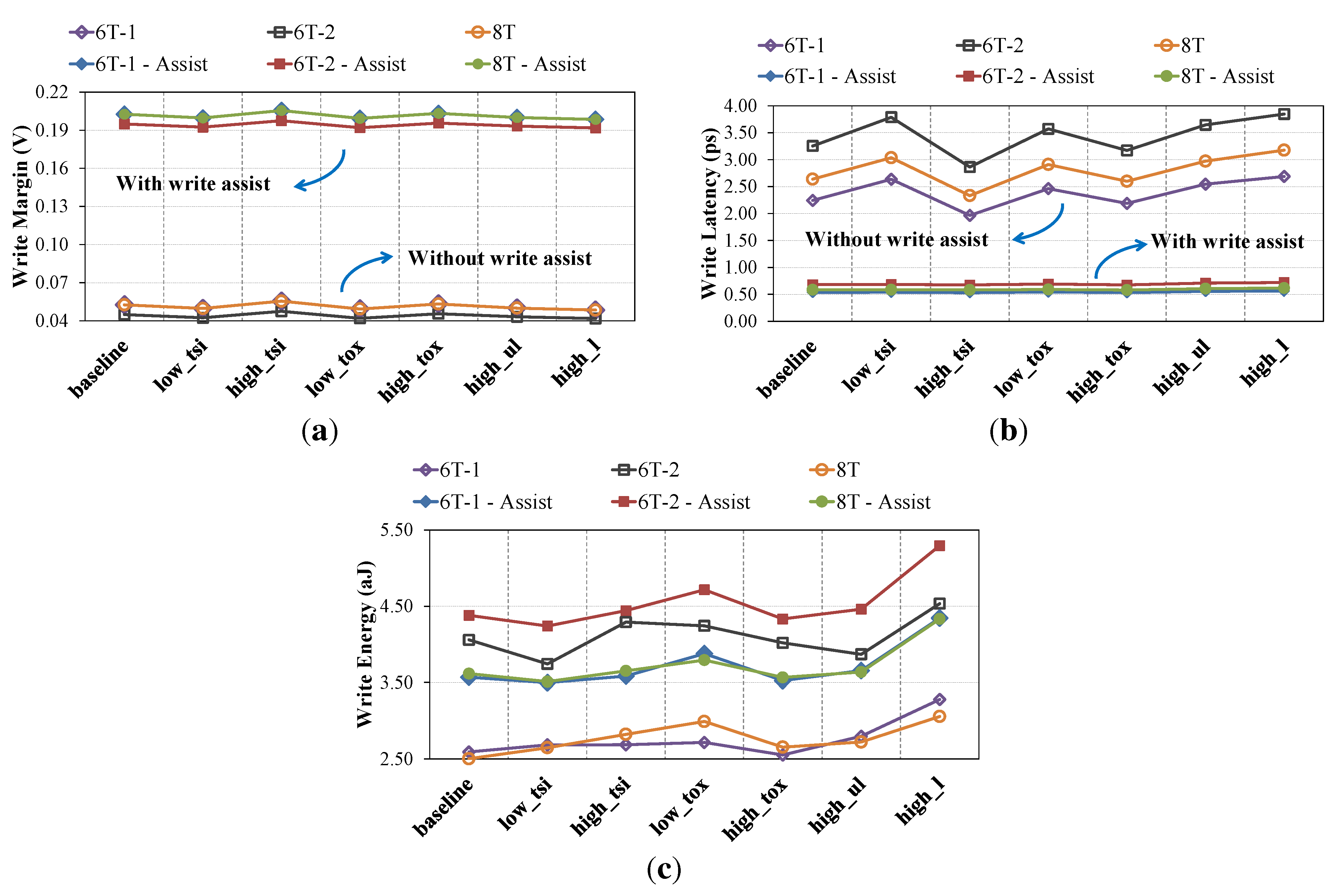
3.2. Circuit-Level Comparison

Figure Figure 6b shows the layout area of different SRAM cells made of 7-nm FinFET devices. As shown in the figure, only 6T-1 and 6T-2 have smaller layout areas than the 8T SRAM, and hence, in the rest of this paper, we will only show the results of the 6T-1, 6T-2 and 8T cells. The 8T SRAM cell has a very high read SNM, which comes at the cost of a 40% and 17% larger area than 6T-1 and 6T-2 SRAMs, respectively. On the other hand, adopting high_l devices instead of the baseline increases the area of SRAM cells by ∼3%. Therefore, the 8T SRAM made of high_l devices has a 44% larger area compared to the 6T-1 SRAM using the baseline device. Other characteristics of SRAM cells under super- and near-threshold operations are shown in Figure 7.
Figure 7. Characteristics of SRAM cells using different 7-nm FinFET devices undersuper-( V d d = 450 mV) and near-threshold ( V d d = 300 mV) regimes: (a) hold and (b) read static noise margins; (c) write margin; (d) idle-mode leakage power; (e) read and (f) write access latencies; and (g) read and (h) write access energies.
Jlpea 05 00165 g007
From Figure 7b, we can observe the excellent read SNM of the 8T SRAM even under the near-threshold operation. More specifically, under the super-threshold (near-threshold) regime and using baseline devices, the read SNM of 8T is 2.34× (2.14×) and 2.08× (1.93×) higher than that of 6T-1 and 6T-2 SRAMs, respectively. On the other hand, adopting high_l devices improves the SNM by 4% in both super- and near-threshold regimes. In general, the SNM is higher if the corresponding FinFET device has a higher ON/OFF current ratio. Hence, the highest SNM is achieved by the 8T SRAM cell using high_l devices. The leakage power of SRAM cell depends on the OFF current of the underlying FinFET devices, and thus, the lowest leakage power is achieved when SRAM cells adopt high_l devices. Moreover, because of using all single-fin transistors, 6T-1 and 8T SRAM cells have the same leakage power consumption.
Write-assist scheme: The major problem in Figure 7 is the write operation under the near-threshold regime. As we mentioned earlier, the similar strengths of NFET and PFET devices in near-threshold regime degrades the write margin of the SRAM cells. In order to enhance the write margin of near-threshold operation, we use 0.45 V ( V d d of the super-threshold operation) as the voltage level of the word-line during the write operation. This assist scheme (known as word-line boosting) significantly makes access transistor stronger during the write operation, which in turn increases the write margin, as well as the write latency, but at the cost of higher write access energy (cf. Figure 8).
Figure 8. (a) Write margin; (b) write access latency; and (c) write access energy after applying the proposed write-assist technique for near-threshold ( V d d = 300 mV) operation. Since access transistors become stronger during the write operation; write margin and write access latency are improved, but these come at the cost of higher write access energy.
Jlpea 05 00165 g008

4. Architecture-Level Design and Evaluation

We finally compare architecture-level properties of Level 1 (L1) cache memories composed of all different combinations of our FinFET devices and SRAM cells. Although the 6T-1 SRAM cell has a very low read SNM in our 7-nm FinFET technology, the characteristics of cache memories made of the 6T-1 SRAM cell are reported for comparison purposes in this section.

4.1. Cache Memories

CACTI [16] is a widely-used cache modeling tool, but it does not support FinFET devices and 8T SRAM cells. Therefore, in order to assess cache memories manufactured with deeply-scaled FinFET devices, we adopt a modified version of CACTI with FinFET and 8T SRAM support [17]. A newer version of this tool, called P-CACTI [18], also supports XML interfaces, which are used for introducing new technology and/or device parameters. Since our optimizations involve extensive simulations exploiting different 7-nm FinFET devices, these XML inputs are extremely helpful in simplifying and also speeding up the process.
For the simulations in this section, we adopt L1 data (L1-D) and L1 instruction (L1-I) cache memories with the following configurations: 16 KB, two-way set-associative, one bank, 64 Byte line and implementing the least recently used (LRU) replacement policy. For each combination of FinFET device and SRAM cell, the cache structure (i.e., the number of rows and columns of the SRAM sub-array) with the minimum energy-delay product is found. We use the Sniper [19] multi-core simulator to derive the number of cache accesses, as well as the total number of instructions for various applications from the PARSEC [20] and SPLASH2 [21] benchmark suite. We use these performance statistics in order to obtain the average cache access ratio, r, which will be used subsequently to calculate the total power consumption, P t o t a l , as well as the energy consumption per cycle, E c a c h e , of the cache memory:
r = number of cache accesses total number of instructions
P t o t a l = r · P d y n a m i c + P l e a k a g e
E c a c h e = P t o t a l · t c y c l e
where P d y n a m i c , P l e a k a g e and t c y c l e are the dynamic power, leakage power and cycle time (i.e., the minimum time between two consecutive accesses to the cache) of the cache memory, respectively, which are obtained from the P-CACTI tool. Furthermore, the energy-delay product is calculated as E c a c h e × t c y c l e . Based on our simulations, average cache ratios of L1-I and L1-D are 12% and 34%, respectively. Moreover, L1-I and L1-D results are summed up and shown as L1.

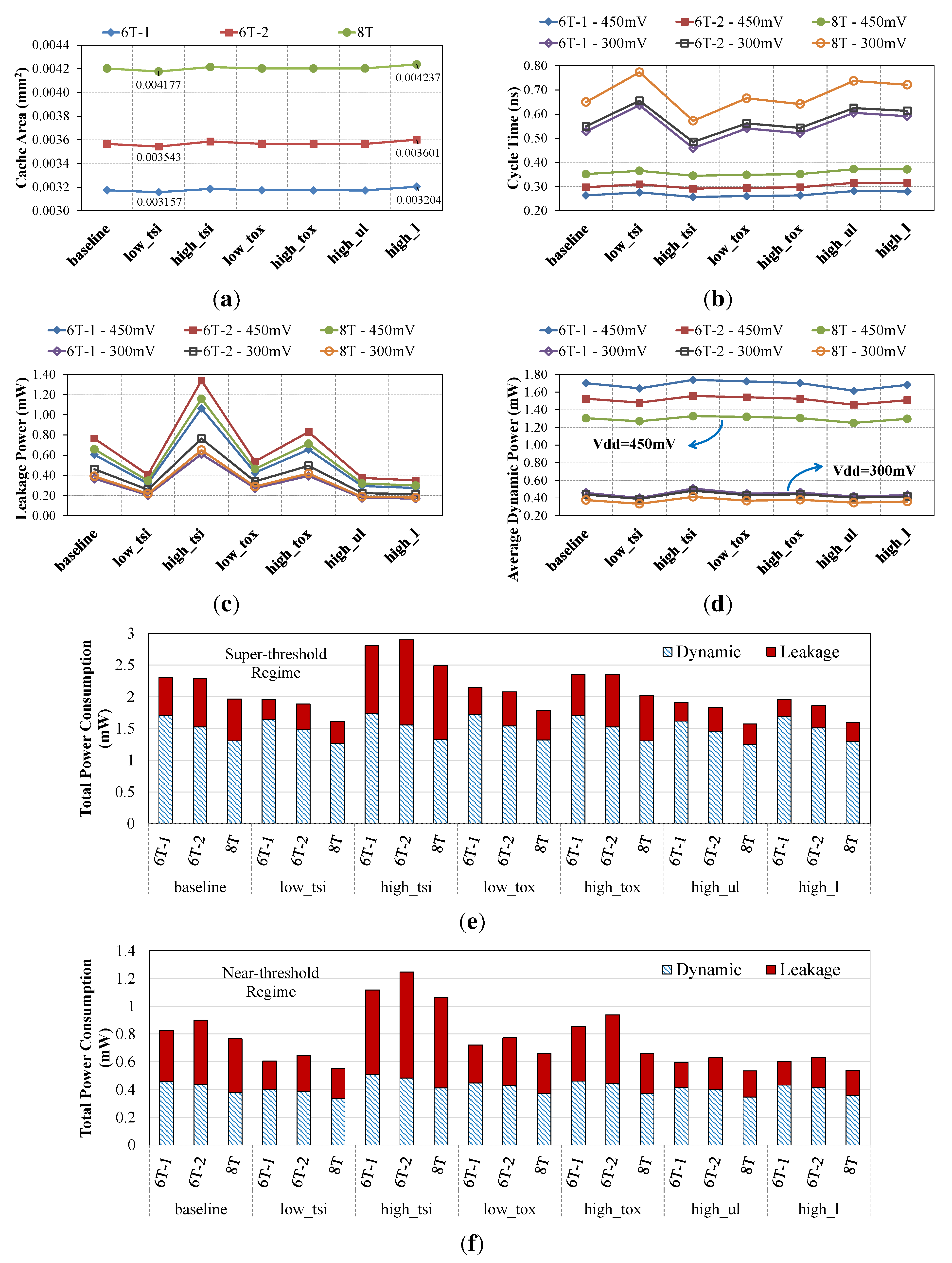
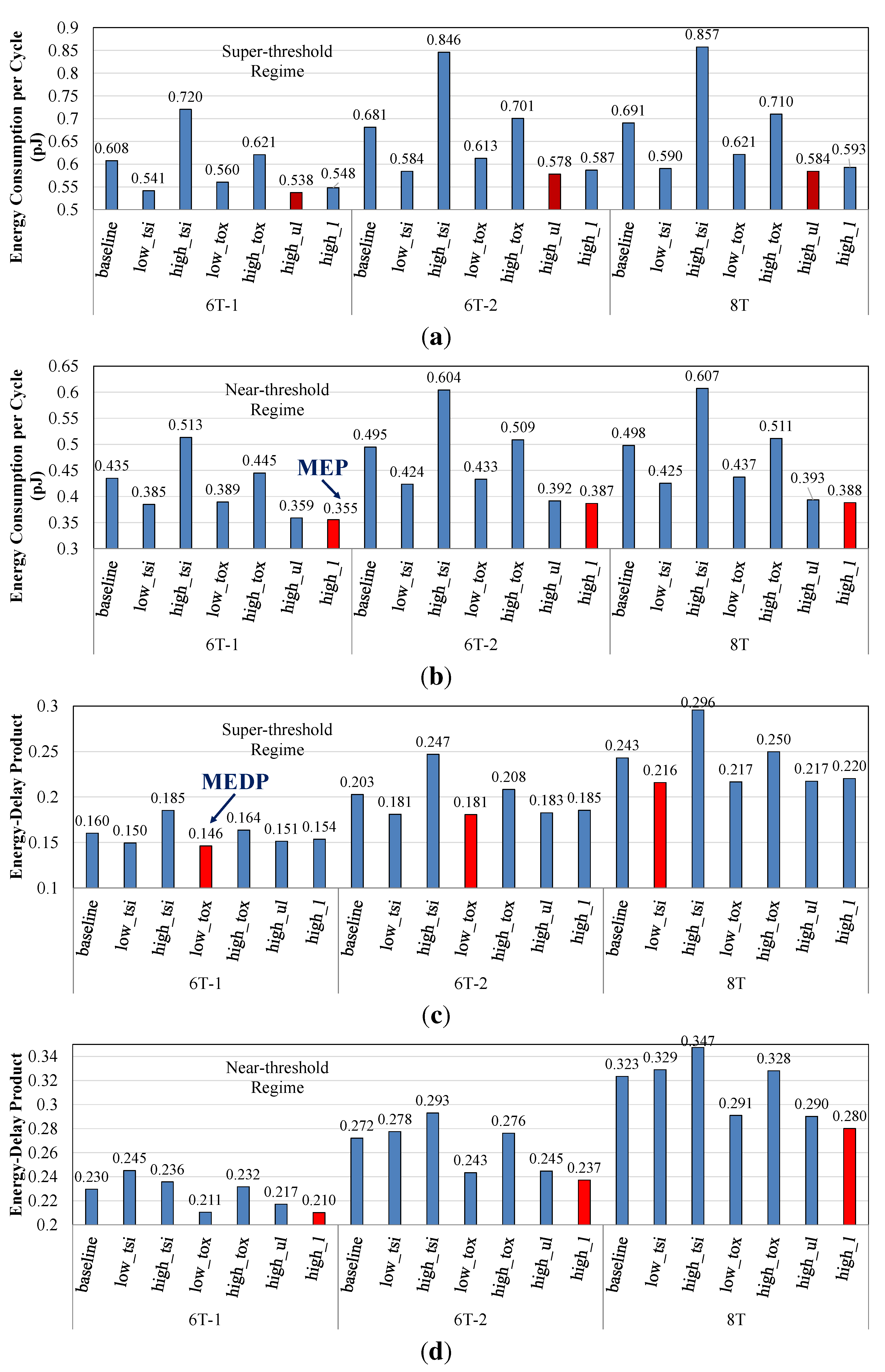
4.2. Architecture-Level Comparison

Characteristics of the L1 cache, including the area, cycle time, leakage, average dynamic and total power consumptions under super- and near-threshold regimes, are reported in Figure 9. As we mentioned in Section 3, the 8T SRAM cell has a 40% larger area than the 6T-1 cell. However, at the cache-level, adopting 8T SRAMs results in 32% area overhead compared to L1 caches made of 6T-1 cells (Figure 9a). This is because the area overhead of peripheral circuits (which consume ∼20% of the cache area) in cache memories made of 8T SRAMs is negligible. On the other hand, cycle time is mainly determined by the ON current of the underlying device, and hence, the shortest cycle time is achieved by using high_tsi devices (Figure 9b). More precisely, among different combinations of our FinFET devices and SRAM cell designs, using the 6T-1 SRAM cell with the high_tsi device operating at super-threshold regime results in the fastest L1 cache with a clock frequency of 3.89 GHz, which is 34% higher than the fastest L1 cache made of 8T cells. However, by ignoring the 6T-1 SRAM and just considering the stable cache memories, the fastest L1 cache is achieved by adopting the 6T-2 SRAM cell with the high_tsi device operating at the super-threshold regime, which is 18% higher than the fastest L1 cache made of 8T cells. In fact, the smaller footprint of an SRAM cell not only improves the memory density (which means more bits on the unit area), but also significantly impacts the cache access latency and access energy. The reason is because smaller SRAM cells also cause word-lines and bit-lines to become shorter, which means less resistance and capacitance on word-lines and bit-lines.
Better memory density, faster clock frequency and lower access energy consumption make the 6T SRAM a desired memory cell for cache memories. However, the main drawback of the 6T SRAM cell (especially the 6T-1 cell) is its poor read SNM (i.e., low data stability), which results in failure, especially under deeply-scaled technologies, where the impact of process variations is increasing. That is why the 8T SRAM cell design [15] has been proposed as a circuit-level solution in order to enhance the stability of the SRAM cell. Accordingly, because of the data stability requirements, the 8T SRAM cell becomes the choice of memory cell for our 7-nm FinFET technology. However, it is worth mentioning that other solutions for enhancing the cell stability with small impact on the cache area (or even in some cases, with no area overhead) exist, such as: (i) using read/write-assist techniques [22,23,24]; and (ii) taking the advantage of the independent gate control of FinFET devices [9]. Such solutions may not achieve the excellent read SNM of the 8T SRAM cell, but still show high yields under process variations [22,25].
The leakage power of the SRAM cell, which mainly depends on the OFF current of the adopted device, is the major component of the cache leakage power. Accordingly, the high_l device achieves the lowest cache leakage power consumption (Figure 9c). Moreover, due to the usage of all single-fin transistors, 6T-1 and 8T cells experience less power consumption compared to the 6T-2 SRAM cell. Furthermore, by looking at Figure 9e, we notice that the dynamic power is the main component of the total power consumption of the L1 cache memory, which is due to the high access ratio of L1 cache, especially L1-D. On the other hand, because of the quadratic dependence of dynamic power on V d d , operating at the near-threshold regime is very effective in terms of dynamic power reduction (3.6× on average), but has a smaller impact on reducing the leakage power (1.7× on average). For L2 and L3 cache memories, the leakage power becomes the dominant component of the cache power consumption, which is due to the following reasons: (i) L2 and L3 caches are larger than L1 and, hence, have a larger number of SRAM cells, which means more leakage paths during idle mode; and (ii) L2 and L3 also have very low access ratios (e.g., 2% in L2) and, thus, are idle most of the time. Therefore, low leakage FinFET devices are more desirable for L2 and L3 cache memories.
In order to better evaluate our L1 cache memories, access energy consumption per cycle and energy-delay product values of each L1 cache are shown in Figure 10.
Figure 9. Characteristics of the Level 1 (L1) cache memory using different SRAM cells and 7-nm FinFET devices under super-( V d d = 450 mV) and near-threshold ( V d d = 300 mV) regimes: (a) cache area; (b) cycle time; (c) leakage power; (d) average dynamic power consumption, and total power consumption in (e) super- and (f) near-threshold regimes.
Jlpea 05 00165 g009
Figure 10. Energy consumption per cycle under (a) super- and (b) near-threshold regimes and the energy-delay product under (c) super- and (d) near-threshold regimes for the L1 cache memory using different SRAM cells and 7-nm FinFET devices. In each figure, the minimum point under each SRAM cell is highlighted with red color.
Jlpea 05 00165 g010
In each figure, the minimum value for each SRAM cell is highlighted in red color. The lowest access energy consumption under the super-threshold regime is achieved by using high_ul devices and under the near-threshold regime is obtained by using high_l devices. The V d d reduction in the near-threshold operation further reduces the energy consumption, and as a result, L1 cache memories made of high_l devices and operating at near-threshold regime result in the minimum energy point (MEP). Comparing the L1 cache memory that achieves the MEP with the L1 cache made of baseline devices and operating at super-threshold regime shows a 71% (78%) improvement in the energy-efficiency when 6T-1 (8T) SRAM cells are used. On the other hand, the minimum energy-delay product point (MEDP) is achieved by using low_tox devices for 6T-1 and by using low_tsi devices for 8T SRAM cell, both operating at the super-threshold regime.

5. Conclusions and Future Work

Seven FinFET devices optimized for a 7-nm process technology along with three SRAM cells were evaluated and compared using our cross-layer design framework. The high_l device has the lowest OFF current and the highest ON/OFF current ratio. Moreover, the 8T SRAM cell achieves the highest noise margins, which guarantees its robust operation. At the cache level, it is observed that L1 cache memory made of high_l devices operating at the near-threshold regime achieves the minimum energy operation point, whereas cache memories made of high_tsi (high_tox) devices for the 8T (6T-1) SRAM cell operating at the super-threshold regime achieve the minimum energy-delay product point. The 8T SRAM cell has an excellent read SNM, and thus, the 8T SRAM is the preferred choice of memory cell due to reliability considerations. On the other hand, because of smaller layout area, the all single-fin 6T SRAM cell achieves higher memory density and lower access latency and energy consumption. As a result, the efficient usage of (i) read/write-assist circuits and/or (ii) the independent gate control feature of FinFET devices (if such devices are provided by the underlying technology process) is significantly important in order to enhance the robust operation of the 6T-1 SRAM cell and, hence, to increase the energy efficiency of cache memories.
Future Work: Because of the significance of process variations in deeply-scaled technology nodes [26], we intend to extend the proposed framework to support variability analysis. For this purpose, the following steps will be added:
  • Device-level variability analysis: By assuming a Gaussian distribution for L F I N , T S I , work function and doping concentration, as well as proper standard deviation values for each parameter, we can perform Monte Carlo simulations in TCAD in order to derive the distributions of the threshold voltage and drain-source current for our FinFET devices. Lookup tables are still extracted for nominal values.
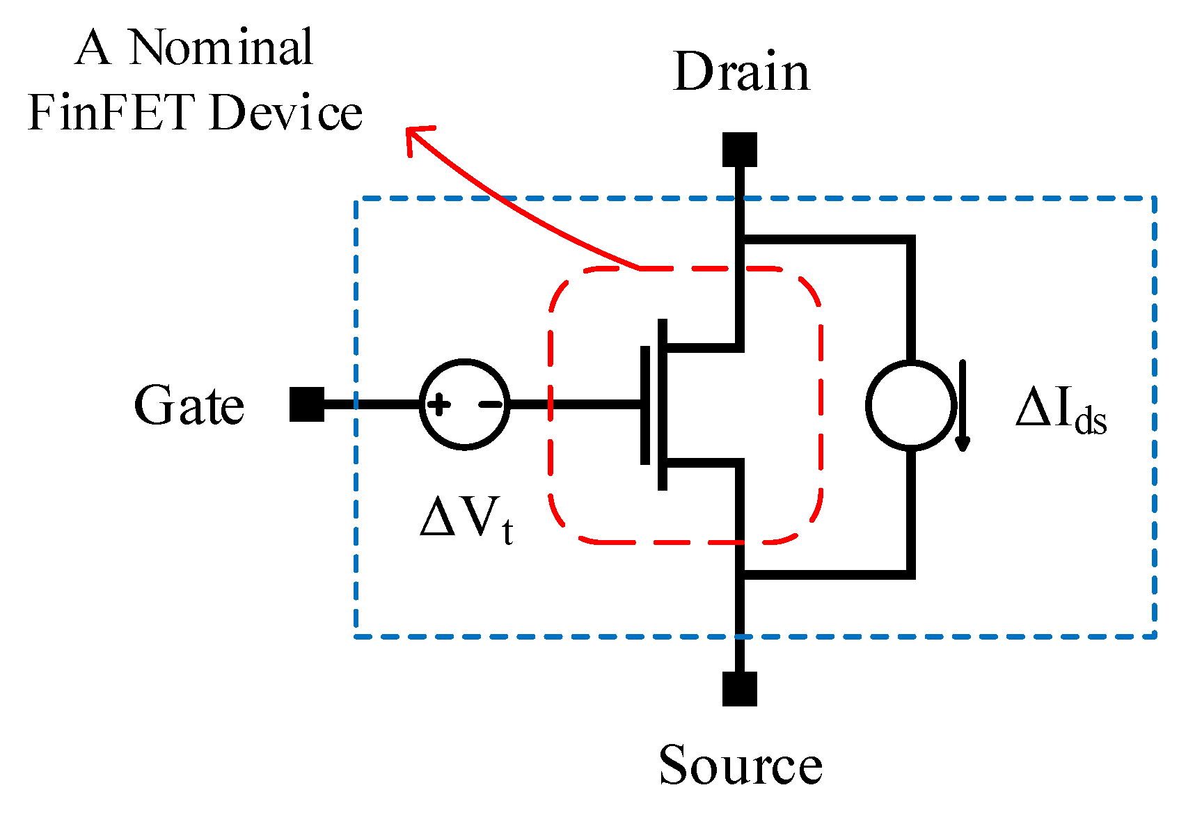
  • Variability analysis of SRAM cells: Each transistor of the SRAM cell is modeled as shown in Figure 11 [27]. More specifically: (i) a voltage source is inserted on the gate terminal in order to inject variations on the threshold voltage; and (ii) a current source is added between drain and source terminals in order to introduce variations on the saturation current. Next, Monte Carlo simulations on N samples are performed, and for each sample, the hold/read/write SNMs are measured using HSpice simulations. Mean, μ, and standard deviation, σ, for each operation are then calculated. For a high-yield SRAM cell, we should have μ / σ 6 . However, using an error-correcting code (ECC) may relax the threshold value of the μ / σ . Furthermore, to speed-up the circuit-level Monte Carlo simulations, importance sampling or stratified sampling canbe adopted.
Figure 11. Modeling process variations in lookup table-based FinFET devices.
Jlpea 05 00165 g011
To study the effect of process variations on the cache-level characteristics, the models introduced in [28] can be integrated into the proposed framework.

Acknowledgments

This work is supported by grants from the PERFECT program of the Defense Advanced Research Projects Agency and the Software and Hardware Foundations of the National Science Foundation.

Author Contributions

FinFET devices are designed and simulated by Shuang Chen and Yanzhi Wang. Circuit simulation are done by Alireza Shafaei and Yanzhi Wang. Architecture-level simulation are done by Alireza Shafaei. The paper is written by Alireza Shafaei, Yanzhi Wang, and Massoud Pedram.

Conflicts of Interest

The authors declare no conflict of interest.

References

  1. Nowak, E.; Aller, I.; Ludwig, T.; Kim, K.; Joshi, R.; Chuang, C.T.; Bernstein, K.; Puri, R. Turning Silicon on its Edge [Double Gate CMOS/FinFET Technology]. IEEE Circuits Devices Mag. 2004, 20, 20–31. [Google Scholar] [CrossRef]
  2. Tang, S.; Chang, L.; Lindert, N.; Choi, Y.K.; Lee, W.C.; Huang, X.; Subramanian, V.; Bokor, J.; King, T.J.; Hu, C. FinFET—A Quasi-Planar Double-Gate MOSFET. In Proceedings of the IEEE International Solid-State Circuits Conference (ISSCC), San Francisco, CA, USA, 5–7 February 2001; pp. 118–119.
  3. Matsukawa, T.; O’uchi, S.; Endo, K.; Ishikawa, Y.; Yamauchi, H.; Liu, Y.X.; Tsukada, J.; Sakamoto, K.; Masahara, M. Comprehensive Analysis of Variability Sources of FinFET Characteristics. In Proceedings of the Symposium on VLSI Technology, Honolulu, HI, USA, 16–18 June 2009; pp. 118–119.
  4. Wang, X.; Brown, A.; Cheng, B.; Asenov, A. Statistical Variability and Reliability in Nanoscale FinFETs. In Proceedings of the IEEE International Electron Devices Meeting (IEDM), Washington, DC, USA, 5–7 December 2011; pp. 5.4.1–5.4.4.
  5. Lin, X.; Wang, Y.; Pedram, M. Joint sizing and adaptive independent gate control for FinFET circuits operating in multiple voltage regimes using the logical effort method. In Proceedings of the IEEE/ACM International Conference on Computer-Aided Design (ICCAD), San Jose, CA, USA, 18–21 November 2013; pp. 444–449.
  6. Pilo, H.; Arsovski, I.; Batson, K.; Braceras, G.; Gabric, J.; Houle, R.; Lamphier, S.; Radens, C.; Seferagic, A. A 64 Mb SRAM in 32 nm High-k Metal-Gate SOI Technology with 0.7 V Operation Enabled by Stability, Write-Ability and Read-Ability Enhancements. IEEE J. Solid State Circuits 2012, 47, 97–106. [Google Scholar]
  7. Pilo, H.; Adams, C.; Arsovski, I.; Houle, R.; Lamphier, S.; Lee, M.; Pavlik, F.; Sambatur, S.; Seferagic, A.; Wu, R.; et al. A 64Mb SRAM in 22 nm SOI technology featuring fine-granularity power gating and low-energy power-supply-partition techniques for 37% leakage reduction. In Proceedings of the IEEE International Solid-State Circuits Conference (ISSCC), San Francisco, CA, USA, 17–21 February 2013; pp. 322–323.
  8. Baravelli, E.; Marchi, L.D.; Speciale, N. {VDD} Scalability of FinFET SRAMs: Robustness of Different Design Options against LER-induced Variations. Solid State Electron. 2010, 54, 909–918. [Google Scholar] [CrossRef]
  9. Guo, Z.; Balasubramanian, S.; Zlatanovici, R.; King, T.J.; Nikolic, B. FinFET-based SRAM design. In Proceedings of the International Symposium on Low Power Electronics and Design (ISLPED), San Diego, CA, USA, 8–10 August 2005; pp. 2–7.
  10. Synopsys Technology Computer-Aided Design (TCAD). Available online: http://www.synopsys.com/tools/tcad (accessed on 31 July 2015).
  11. Goud, A.; Gupta, S.; Choday, S.; Roy, K. Atomistic tight-binding based evaluation of impact of gate underlap on source to drain tunneling in 5 nm gate length Si FinFETs. In Proceedings of the 71st Annual Device Research Conference (DRC), Notre Dame, IN, USA, 23–26 June 2013.
  12. Chen, S.; Wang, Y.; Lin, X.; Xie, Q.; Pedram, M. Performance prediction for multiple-threshold 7nm-FinFET-based circuits operating in multiple voltage regimes using a cross-layer simulation framework. In Proceedings of the IEEE SOI-3D-Subthreshold Microelectronics Technology Unified Conference (S3S), Millbrae, CA, USA, 6–9 October 2014.
  13. Gupta, P.; Kahng, A.B.; Sharma, P.; Sylvester, D. Selective Gate-length Biasing for Cost-effective Runtime Leakage Control. In Proceedings of the Design Automation Conference (DAC), San Diego, CA, USA, 7–11 June 2004; pp. 327–330.
  14. Seevinck, E.; List, F.; Lohstroh, J. Static-Noise Margin Analysis of MOS SRAM Cells. IEEE J. Solid State Circuits 1987, 22, 748–754. [Google Scholar] [CrossRef]
  15. Chang, L.; Fried, D.; Hergenrother, J.; Sleight, J.; Dennard, R.; Montoye, R.; Sekaric, L.; McNab, S.; Topol, A.; Adams, C.; et al. Stable SRAM Cell Design for the 32 nm Node and Beyond. In Proceedings of the Symposium on VLSI Technology, Kyoto, Japan, 14–16 June 2005; pp. 128–129.
  16. Muralimanohar, N.; Balasubramonian, R.; Jouppi, N. Optimizing NUCA Organizations and Wiring Alternatives for Large Caches with CACTI 6.0. In Proceedings of the 40th Annual IEEE/ACM International Symposium on Microarchitecture (MICRO), Chicago, IL, USA, 1–5 December 2007; pp. 3–14.
  17. Shafaei, A.; Wang, Y.; Lin, X.; Pedram, M. FinCACTI: Architectural Analysis and Modeling of Caches with Deeply-Scaled FinFET Devices. In Proceedings of the IEEE Computer Society Annual Symposium on VLSI (ISVLSI), Tampa, FL, USA, 9–11 July 2014; pp. 290–295.
  18. P-CACTI. Available online: http://sportlab.usc.edu/download/pcacti/ (accessed on 31 July 2015).
  19. Carlson, T.; Heirman, W.; Eeckhout, L. Sniper: Exploring the level of abstraction for scalable and accurate parallel multi-core simulation. In Proceedings of the International Conference for High Performance Computing. Networking, Storage and Analysis (SC), Seatle, WA, USA, 12–18 November 2011; pp. 1–12.
  20. Bienia, C.; Li, K. PARSEC 2.0: A New Benchmark Suite for Chip-Multiprocessors. In Proceedings of the 5th Annual Workshop on Modeling, Benchmarking and Simulation, Austin, TX, USA, 21 June 2009.
  21. Woo, S.C.; Ohara, M.; Torrie, E.; Singh, J.P.; Gupta, A. The SPLASH-2 Programs: Characterization and Methodological Considerations. In Proceedings of the 22nd Annual International Symposium on Computer Architecture (ISCA), Santa Margherita Ligure, Italy, 22–24 June 1995; pp. 24–36.
  22. Karl, E.; Guo, Z.; Conary, J.; Miller, J.; Ng, Y.G.; Nalam, S.; Kim, D.; Keane, J.; Bhattacharya, U.; Zhang, K. A 0.6V 1.5GHz 84Mb SRAM Design in 14 nm FinFET CMOS Technology. In Proceedings of the IEEE International Solid-State Circuits Conference (ISSCC), San Francisco, CA, USA, 22–26 February 2015; pp. 1–3.
  23. Song, T.; Rim, W.; Jung, J.; Yang, G.; Park, J.; Park, S.; Baek, K.H.; Baek, S.; Oh, S.K.; Jung, J.; et al. A 14 nm FinFET 128Mb 6T SRAM with VMIN-enhancement techniques for low-power applications. In Proceedings of the IEEE International Solid-State Circuits Conference (ISSCC), San Francisco, CA, USA, 9-13 Feb. 2014; pp. 232–233.
  24. Chen, Y.H.; Chan, W.M.; Wu, W.C.; Liao, H.J.; Pan, K.H.; Liaw, J.J.; Chung, T.H.; Li, Q.; Chang, G.; Lin, C.Y.; et al. A 16 nm 128Mb SRAM in high-k metal-gate FinFET technology with write-assist circuitry for low-VMIN applications. In Proceedings of the IEEE International Solid-State Circuits Conference (ISSCC), San Francisco, CA, USA, 9–13 February 2014; pp. 238–239.
  25. Shafaei, A.; Chen, S.; Wang, Y.; Pedram, M. A Cross-Layer Framework for Designing and Optimizing Deeply-Scaled FinFET-Based SRAM Cells under Process Variations. In Proceedings of the 20th Asia and South Pacific Design Automation Conference (ASP-DAC), Chiba, Japan, 19–22 January 2015.
  26. Dierickx, B.; Miranda, M.; Dobrovolny, P.; Kutscherauer, F.; Papanikolaou, A.; Marchal, P. Propagating variability from technology to system level. In Proceedings of the International Workshop on Physics of Semiconductor Devices (IWPSD), Mumbai, India, 16–20 December 2007; pp. 74–79.
  27. Royer, P.; Lopez-Vallejo, M. Using pMOS Pass-Gates to Boost SRAM Performance by Exploiting Strain Effects in Sub-20-nm FinFET Technologies. IEEE Trans. Nanotechnol. 2014, 13, 1226–1233. [Google Scholar] [CrossRef]
  28. Lee, C.Y.; Jha, N. CACTI-FinFET: An integrated delay and power modeling framework for FinFET-based caches under process variations. In Proceedings of the Design Automation Conference (DAC), San Diego, CA, USA, 5–9 June 2011; pp. 866–871.

