Article

A 0.2 V, 23 nW CMOS Temperature Sensor for Ultra-Low-Power IoT Applications

by
Divya Akella Kamakshi
1,*,
Aatmesh Shrivastava
2 and
Benton H. Calhoun
1
1
Department of Electrical and Computer Engineering, University of Virginia, Charlottesville, VA 22904, USA
2
PsiKick Inc., Charlottesville, VA 22902, USA
*
Author to whom correspondence should be addressed.
J. Low Power Electron. Appl. 2016, 6(2), 10; https://doi.org/10.3390/jlpea6020010
Submission received: 1 April 2016 / Revised: 20 May 2016 / Accepted: 6 June 2016 / Published: 15 June 2016
(This article belongs to the Special Issue Selected Papers from IEEE S3S Conference 2015)

Abstract

:
We propose a fully on-chip CMOS temperature sensor in which a sub-threshold (sub-VT) proportional-to-absolute-temperature (PTAT) current element starves a current-controlled oscillator (CCO). Sub-VT design enables ultra-low-power operation of this temperature sensor. However, such circuits are highly sensitive to process variations, thereby causing varying circuit currents from die to die. We propose a bit-weighted current mirror (BWCM) architecture to resist the effect of process-induced variation in the PTAT current. The analog core constituting the PTAT, the CCO, and the BWCM is operational down to 0.2 V supply voltage. A digital block operational at 0.5 V converts the temperature information into a digital code that can be processed and used by other components in a system-on-chip (SoC). The proposed temperature sensor system also supports resolution-power trade-off for Internet-of-things (IoT) applications with different sampling rates and energy needs. The system power consumption is 23 nW and the maximum temperature inaccuracy is +1.5/−1.7 °C from 0 °C to 100 °C with a two-point calibration. The temperature sensor system was designed in a 130 nm CMOS technology and its total area is 250 × 250 μm2.

1. Introduction

The Internet-of-things (IoT) is a rapidly evolving space in the semiconductor industry. IoT devices focus on a wide range of applications, ranging from personal electronics to sensors for monitoring environmental, physiological, industrial, structural signals, etc. For such IoT devices that are untethered and unobtrusively placed, battery replacement or recharging is a very expensive task. Therefore, battery-less self-powered technology is increasingly gaining attention for maintenance-free operation of IoT devices. Recently, harvesting energy from ambient sources with output voltages as low as 10 mV is possible using boost converters such as [1]. In the presence of harvested energy, the circuits are required to consume ultra-low-power (ULP) and operate from the lowest voltage possible to enable longer device lifetimes.
Voltage scaling is an important knob to enable ULP circuit design. The sub-threshold (sub-VT) region of operation, in which circuits are operated at a supply voltage (VDD) less than the transistor threshold voltage (VT), is becoming an attractive option for ULP operation of sensor nodes in which speed is not the primary concern. In digital circuits, dramatic energy reductions can be achieved due to a quadratic dependence of active energy on VDD. In analog circuits, high VDD is traditionally used for greater headroom requirements. However, recently in ULP systems, analog circuits are now being operated at a lower VDD for power savings and also to directly power the circuits using energy-harvesting methodologies, such as thermoelectric, solar etc. For example, in [2] a 2.4 GHz RF receiver was designed to operate at 300 mV VDD. In [3], it was demonstrated that lowering the amplitude of oscillation reduces the power consumption of a crystal (XTAL) oscillator, and it was designed to operate at voltages as low as 300 mV. Energy-harvesting IoT nodes such as [4] would benefit from such sub-VT analog designs. In this paper, we propose a temperature sensor core that is operational in the sub-VT region.
Ambient temperature is an important sensing modality in recent ULP IoT sensor systems. Various types of temperature sensors based on both bipolar junction transistors (BJTs) and metal–oxide–semiconductor field-effect transistors (MOSFETs) have been recently designed for this purpose. Conventionally, BJT-based temperature sensors take advantage of the complementary-to-absolute temperature (CTAT) property of the base-emitter voltage (VBE) and the proportional-to-absolute temperature (PTAT) property of the difference between two VBE voltages in vertical PNP transistors. However, BJT-based temperature sensors, such as [5], have power consumptions in the μW range, which is not suitable for devices operating from harvested energy. BJT-based temperature sensor architectures also require a higher power supply (1.5 V to 2 V in [5]) that limits the minimum supply voltage in IoT devices.
On the other hand, MOSFET-based temperature sensors [6,7,8,9] are growing in popularity these days for ULP systems. These temperature sensors consume less power in the range of tens to hundreds of nWs as compared to the BJT-based sensors at the expense of accuracy. In [6], a temperature sensor operational from 0.85 V VDD was implemented using dynamic threshold MOS transistors (DTMOSTs) as temperature-sensing devices and an inverter-based zoom ADC to enable a power consumption of 600 nW. In [7], the MOSFET-based temperature sensor consumes only 220 nW while operating continuously. The work in [7] demonstrates techniques to lower power consumption such as sub-VT design, use of frequency-to-digital conversion instead of ADC, an on-chip time reference, etc., which makes this implementation suitable for embedded passive RFID application space. In [8], a CMOS temperature sensor employs a serially-connected sub-VT MOS as a sensing element that is operational from 0.5 V VDD, thereby enabling a power consumption of only 119 nW. In [9], a new temperature sensor topology and changes to conventional voltage-to-current converter and current mirror structures were proposed to achieve a power consumption of 71 nW.
In this paper, we propose to further lower the power consumption of a temperature sensor system with the use of a sub-VT sensor core that consumes very low power and energy and is operational down to 0.2 V VDD [10]. A simplified block diagram of the proposed temperature sensor is shown in 
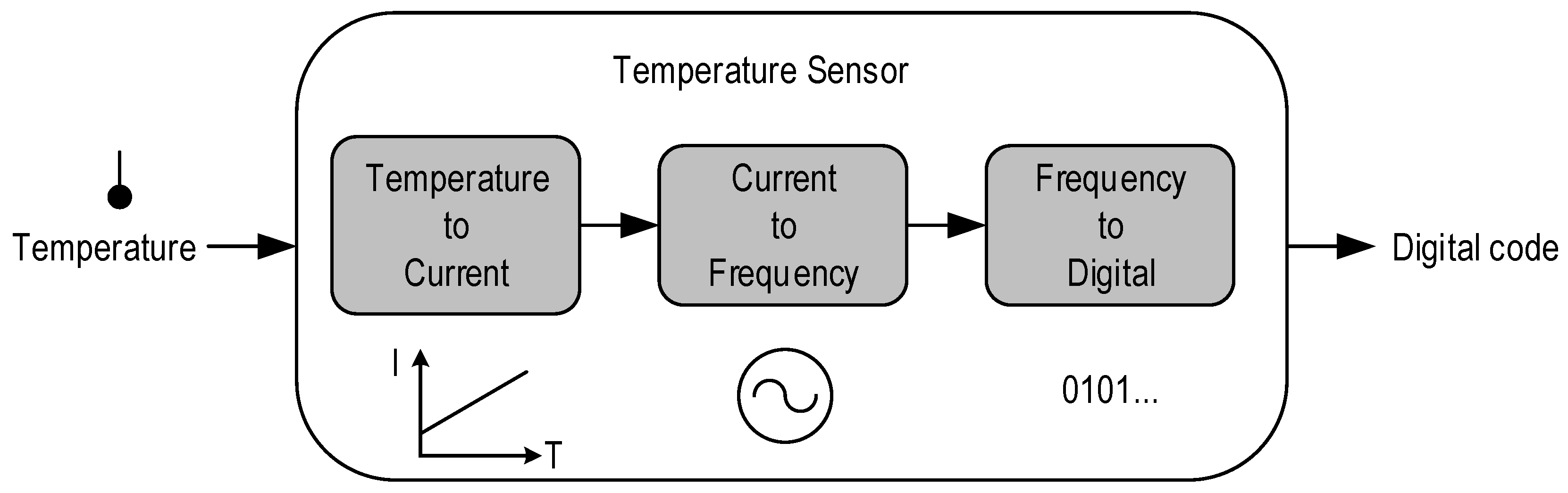
Figure 1. A current proportional to ambient temperature is generated using a sub-VT temperature to current converter. The current is subsequently translated to frequency using a current-controlled oscillator and then into a representative digital code using a digital block, which is usable by any system-on-chip (SoC). Modifications to the conventional current mirror structure enables reduced power consumption in cases such as fast process corners in which power consumption is usually higher than desired. A detailed description of these components is presented in this work.
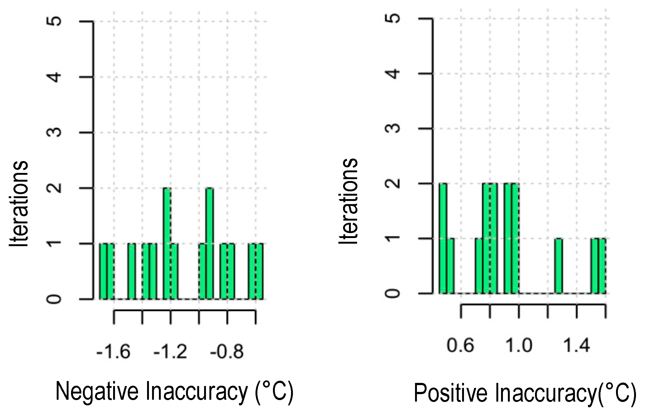
The total power consumption of the temperature sensor system is 23 nW, and the maximum temperature inaccuracy is +1.5/−1.7 °C from 0 °C to 100 °C with a two-point calibration. This paper is structured as follows. Section 2 introduces the temperature sensor architecture and describes the components and the low-power design techniques used. Section 3 presents the simulation results, Section 4 provides a comparison of the proposed system with the state-of-the-art temperature sensors, and finally, Section 5 concludes the work.

2. Components of the Temperature Sensor System

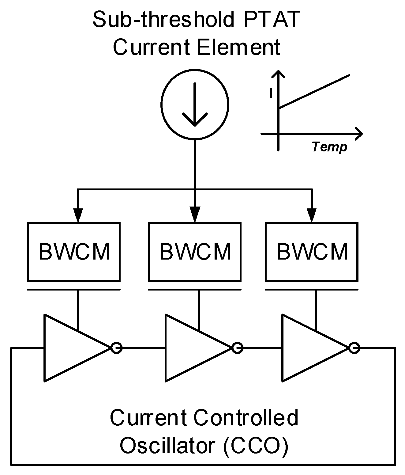
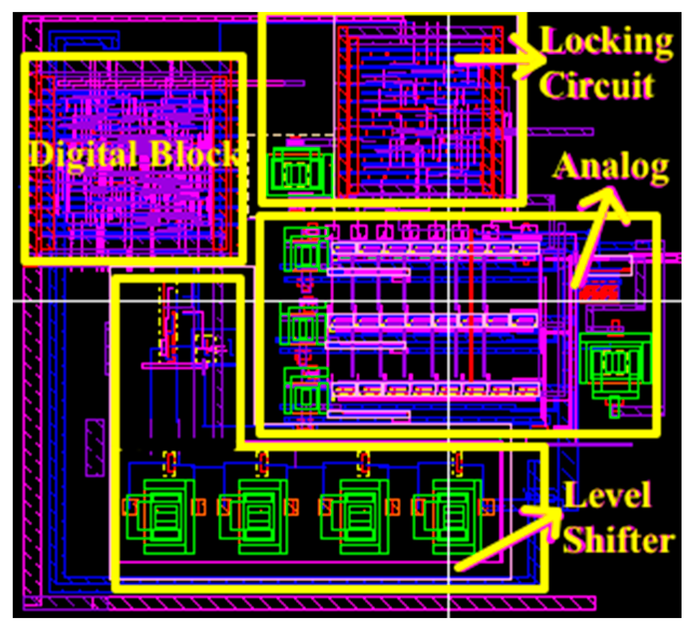
In this paper, we describe the components of the proposed fully on-chip temperature sensor system. A component-level system diagram is shown in Figure 2. The proposed temperature sensor core consists of (a) a sub-VT proportional-to-absolute-temperature (PTAT) current element that generates a current proportional to temperature; (b) a bit-weighted current mirror (BWCM) that mirrors the PTAT current to starve a ring oscillator. Process variations can cause a large amount of variations in the sub-VT PTAT current output. A BWCM consisting of eight current mirror arms can be enabled or disabled to control the PTAT current that is mirrored to the subsequent stages (1× implies same current mirrored, 1/2× implies half the current mirrored, etc.); and (c) a current-controlled oscillator (CCO) that generates a clock frequency proportional to the mirrored PTAT current. The sensor core constituting the above components is operational at 0.2 V VDD.
Additionally, a digital block converts the CCO oscillation frequency to a digital code for processing by any SoC component. The digital block operates at 0.5 V VDD, a higher voltage rail that is typically available for digital processing on SoCs such as [4]. The 0.2 V analog supply can be generated from the 0.5 V supply using a switched-capacitor DC–DC regulator or low drop-out (LDO) regulator. The above components are described in detail in this section.

2.1. Sub-Threshold PTAT Current Element

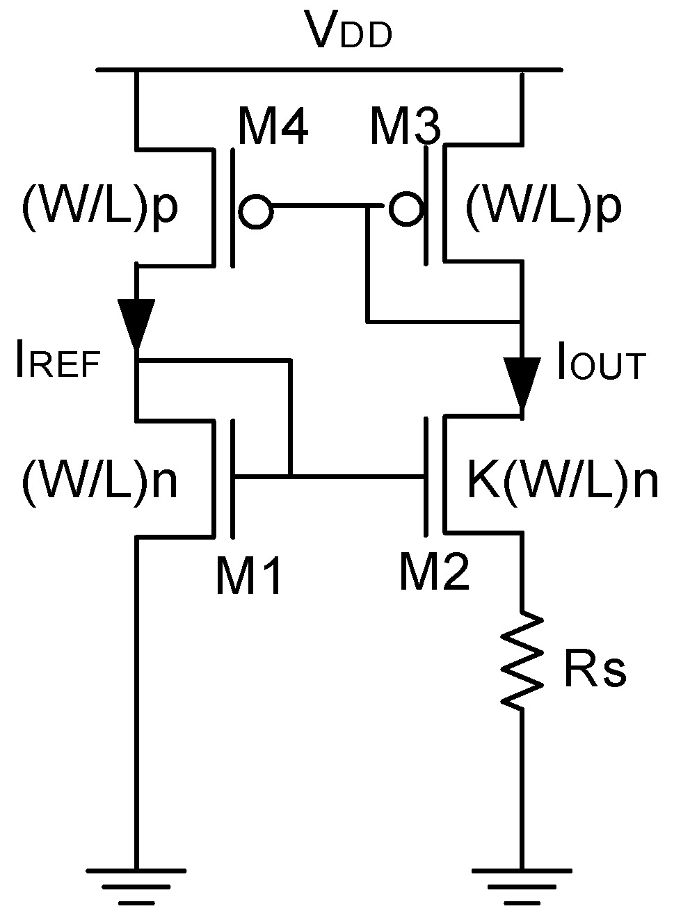
Figure 3 shows the PTAT current source using a single resistor designed to operate at 0.2 V VDD. A PTAT current element generates current that increases linearly with temperature. The transistors M1 to M4 are operated in the sub-VT saturation region.
The PTAT output current and its proportionality to temperature is derived in this section. The drain current of transistors in sub-VT is given by:
IDSUB = Ioexp((VGS − VT)/nφt)(1 − exp(−VDS)/φt)
where Io is drain current when gate-source voltage (VGS) equals VT (Io = µoCox(W/L)(n − 1) φt2), µo is the carrier mobility, Cox is the gate oxide capacitance, W and L are the channel width and length, and n is the sub-VT slope factor. When drain to source voltage VDS > 3φt, the term exp(−VDS)/φt in Equation (1) starts becoming negligible and Equation (1) can be approximated as:
IDSUB = Ioexp((VGS − VT)/nφt)
The transistors in the circuit are sized so that their drain-source voltages (VDS) are greater than 3φtt = kT/q). This is called the sub-VT MOSFET saturation region, in which the drain current becomes independent of VDS. To overcome low headroom at 0.2 V, thin-oxide standard-VT (SVT) devices with typical threshold voltages (VT) of ~0.2 V are used. Long channel lengths are used to reduce short-channel effects. To obtain the equation for PTAT current, Kirchoff’s voltage law is applied to transistors M1, M2, and resistor RS. VGS1 and VGS2 are the gate to source voltages and IDSUB1 and IDSUB2 are the drain currents of transistors M1 and M2, respectively.
VGS1 = VGS2 + IDSUB2RS
Substituting Equation (2) for IDSUB in Equation (3):
tloge(IDSUB1/Io) + VT1 = nφtloge(IDSUB2/KIo) + VT2 + IOUTRS
Since IDSUB1 = IDSUB2 = IOUT and assuming VT1 = VT2 in Equation (4):
IOUT = nφtlogeK/RS
The direct temperature dependence of IOUT on φt (=kT/q) gives a proportional to absolute temperature current. Due to the small values of IOUT current, a smaller resistor as compared to prior PTAT designs can be used. A 400 K poly-silicon resistor with low temperature dependence and operating the PTAT transistors at sub-VT voltages enables generation of currents in the nanoampere range. Such low currents contribute to the low power consumption of the temperature sensor system.
However, sub-VT circuits are highly sensitive to process variations. Process variations can cause output current variations in the sub-VT PTAT. 
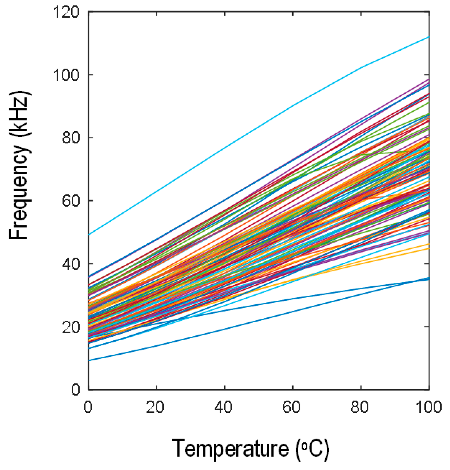
Figure 4 shows a plot of the PTAT current at 27 °C in 100-point Monte Carlo simulations. At higher temperatures, the PTAT current consumption will be higher as it is proportional to temperature. However, the current variation will still exist because of process variation. In the Monte Carlo simulations, both process (inter-die) and mismatch (intra-die) variations were considered. Therefore, it covers the whole range of process variation including typical, slow, and fast corners. We observe that the mean PTAT current is 39 nA, and the 3σ variation of 25 nA is very high. The PTAT current is mirrored into the subsequent current controlled oscillator stage. Therefore, higher PTAT current may cause higher total power dissipation than desired. In the next section, a bit-weighted current mirror (BWCM) is described to decrease such process-induced power dissipation.

2.2. Bit-Weighted Current Mirror

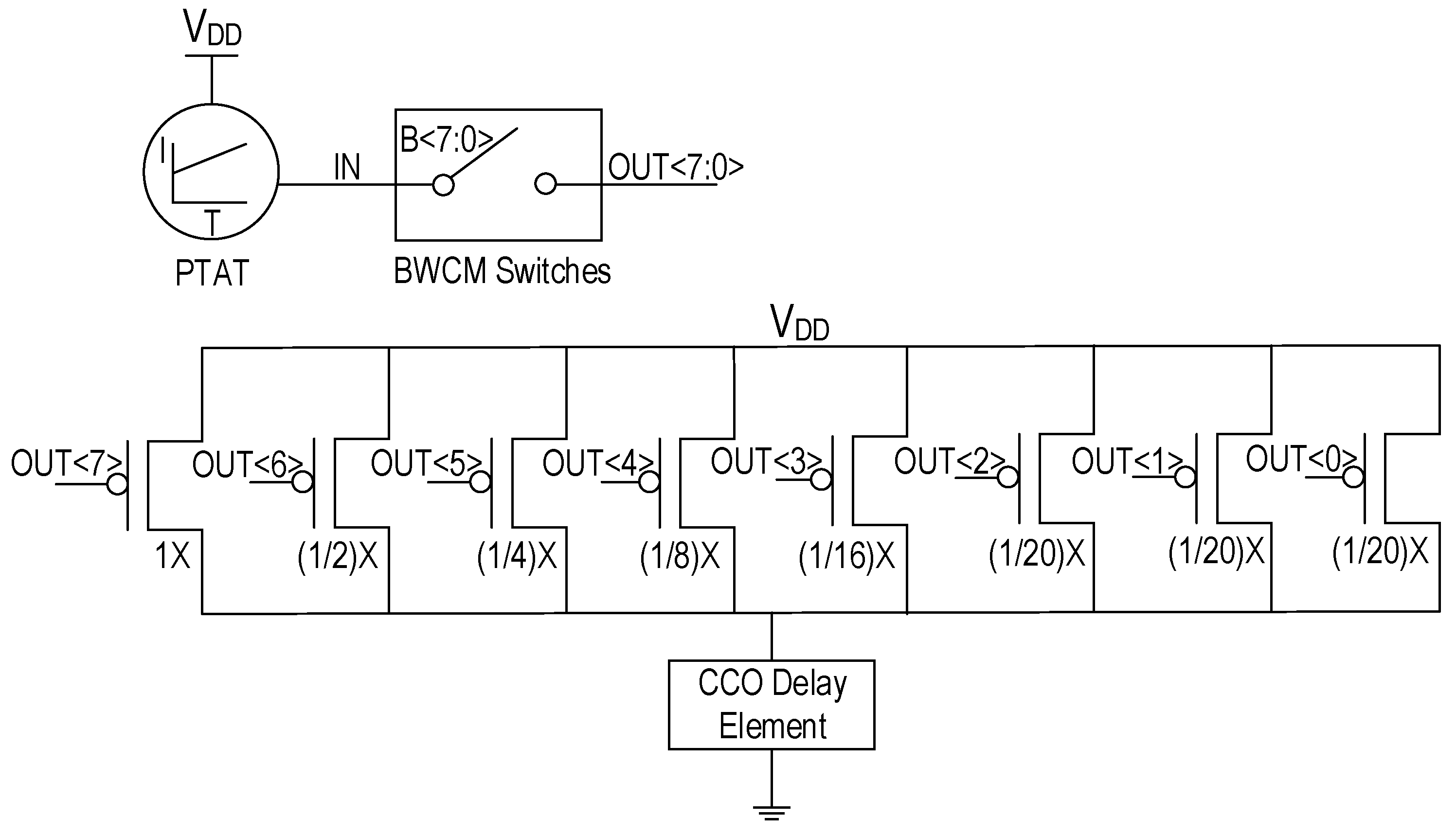
The PTAT current is mirrored using a BWCM to starve the transistors of a CCO as shown in Figure 5, which generates frequencies proportional to temperature.
The BWCM is shown in Figure 6. The BWCM consists of eight current mirror arms, each of them mirroring different fractions of PTAT current to the CCO. For instance, 1x implies that PTAT current is entirely mirrored, 1/2× implies that 50% of the PTAT current is mirrored, and so on. The entire PTAT current is not required to mirror the PTAT linearity information to the CCO, but only a fraction of it that is still linear is sufficient. Furthermore, if the PTAT current is higher than desired due to a strong process, a lower bit setting scales down the BWCM current starving the CCO, thereby enabling power savings. The current mirror arms can be enabled or disabled by bits B<7:0> in the switches. They are not one-hot bits but are binary bits, which implies that different combinations scale the current in different fractions.
However, simple PMOS or NMOS switches cannot be used to enable or disable the current mirror arms at 0.2 V VDD due to effects of high leakage current that interferes with the PTAT current thereby altering its linear characteristics. 
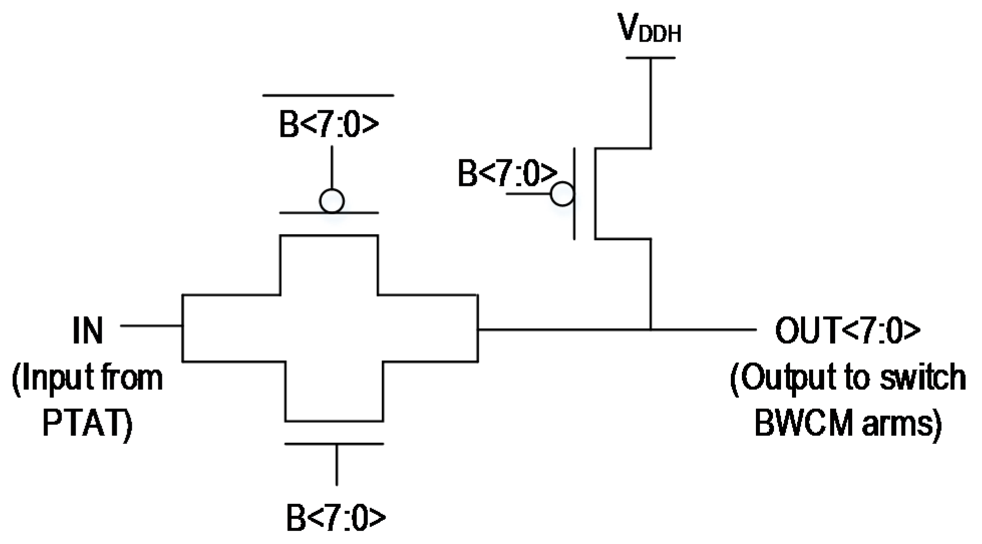
Figure 7 shows the architecture of the BWCM switches used to turn on and off each bit-weighted current mirror arm. To enable an arm, the corresponding transmission gate switch is enabled by one bit of B<7:0>. This creates a path between the PTAT and the enabled current mirror branch. To disable an arm, the output of the switch, and therefore the gate of the PMOS of the corresponding current mirror branch, is pulled high to turn it off.
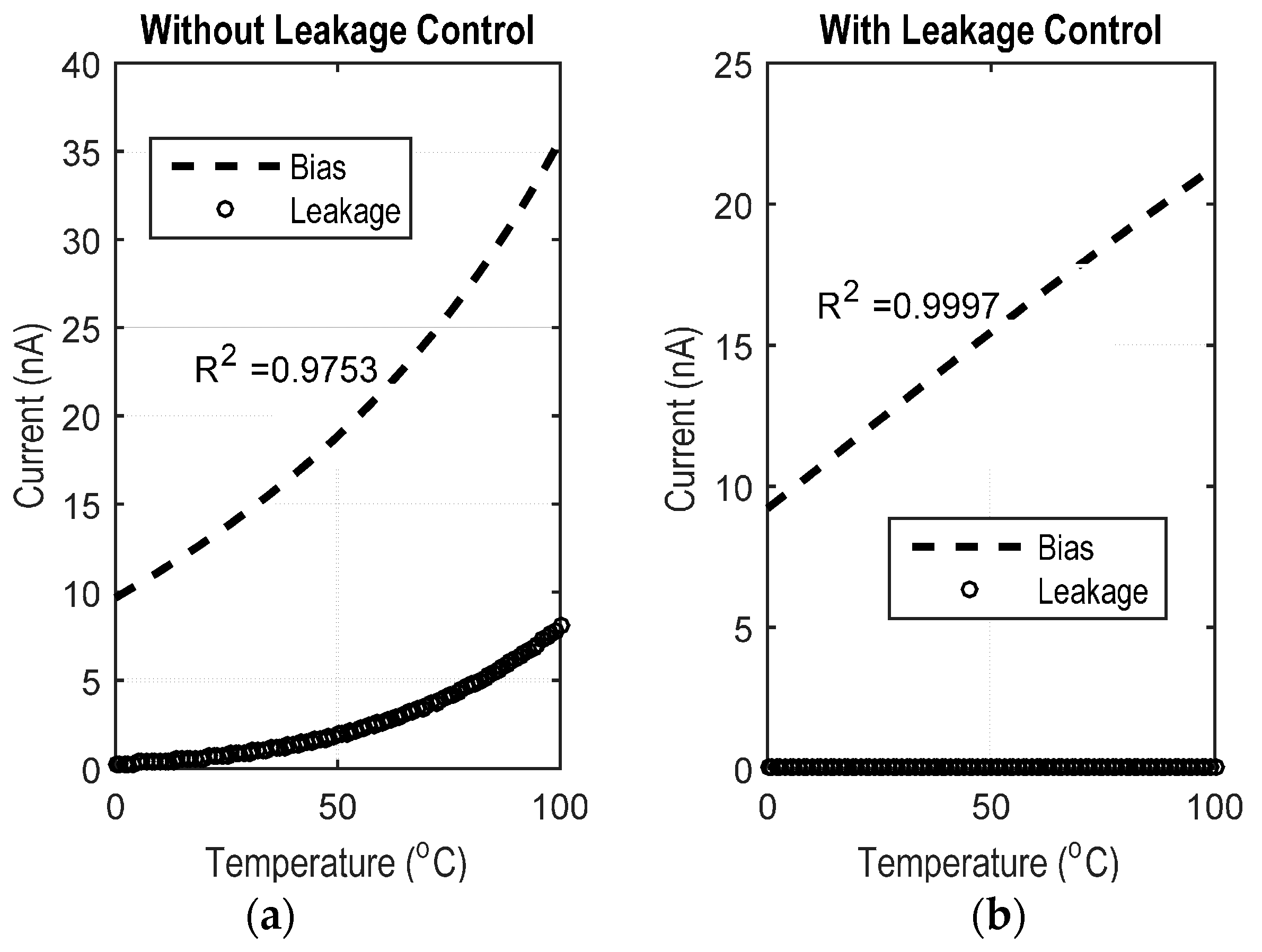
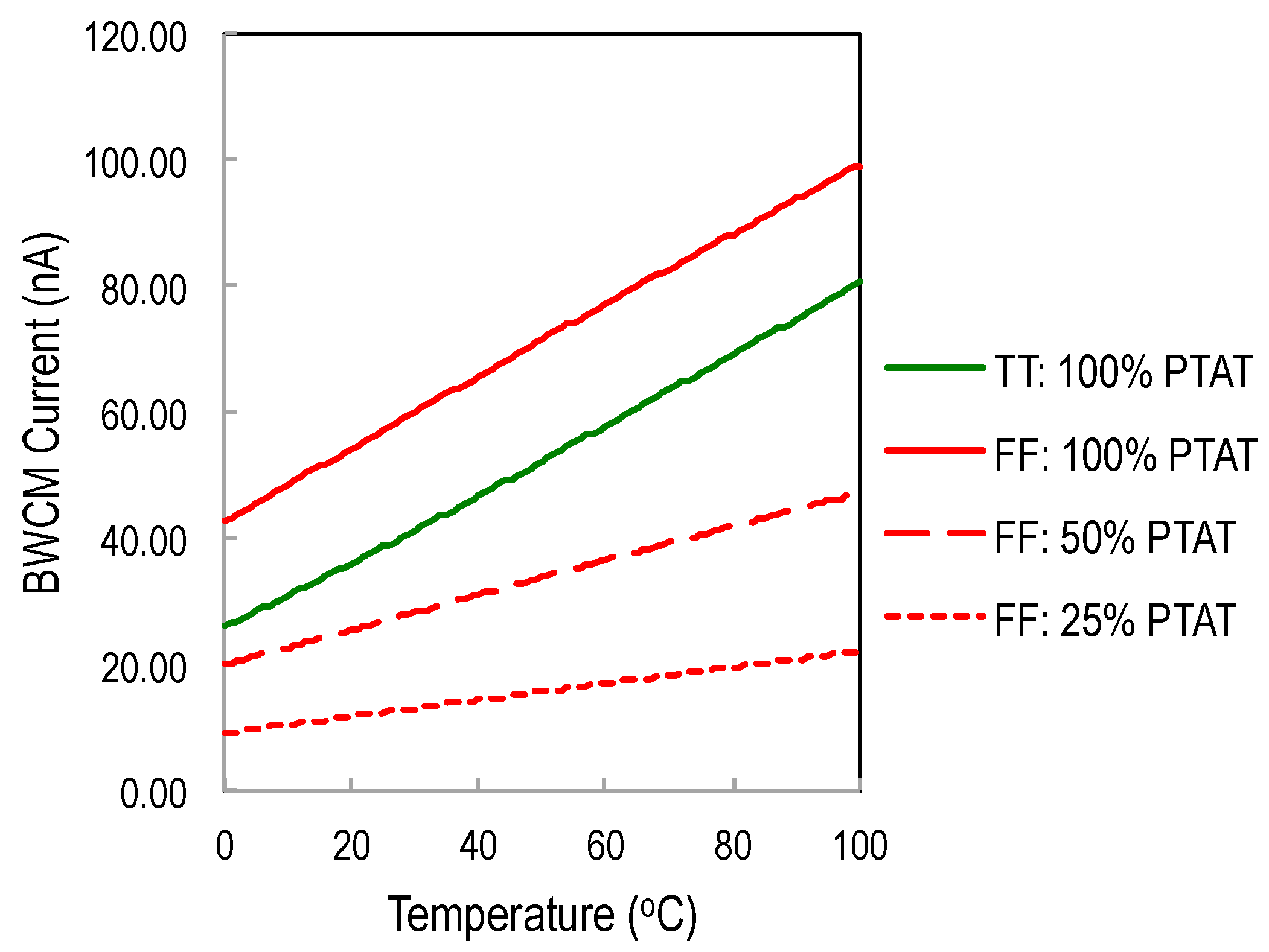
However, when a branch is disabled by pulling the PMOS gate to only 0.2 V VDD, the leakage of the off PMOS transistor is high, thereby causing the effective BWCM current to be non-linear, as shown in Figure 8a. To overcome the leakage, the PMOS of the branch to be disabled is turned off by tying its gate to 0.5 V VDDH (available for digital operation [4]). This negative VGS in the PMOS transistor of the disabled current mirror branch reduces its leakage, thereby keeping the effective BWCM current linear as shown in Figure 8b. The linearity is denoted by R2, a measure of goodness of fit in linear regression. The value of R
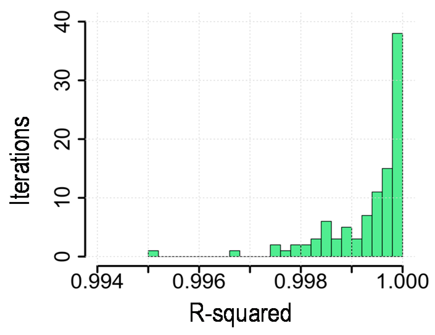
2 lies between 0 and 1. A value closer to 1 indicates higher linearity. The R2 value without leakage control is 0.9753 and with leakage control it improves to 0.9997 for fast process corners and better for other process corners, such as typical or weak.

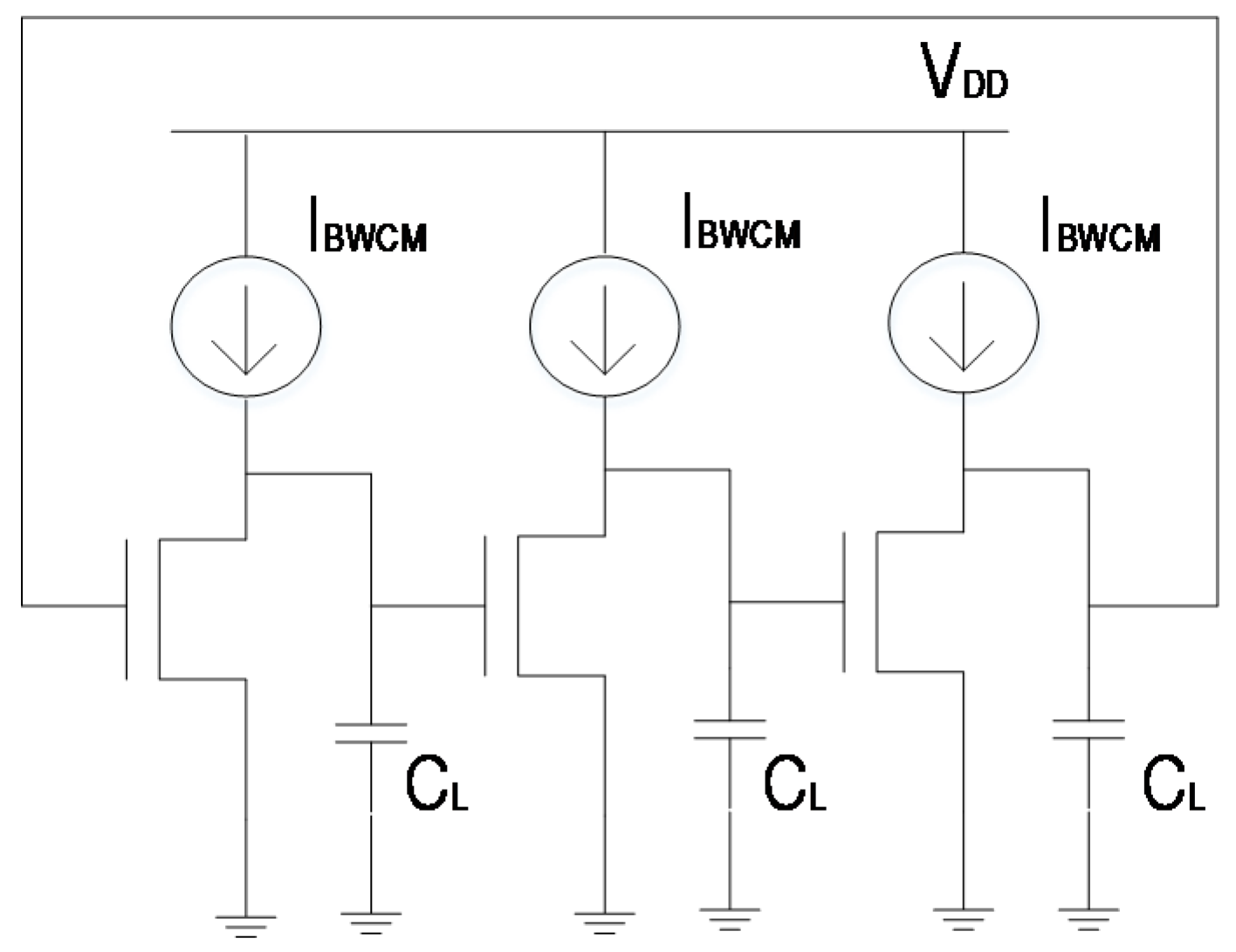
2.3. Current-Controlled Oscillator

A current controlled oscillator (CCO), shown in Figure 9, is starved by the current from the BWCM (IBWCM). It is also possible to mirror the PTAT current to an intermediate BWCM stage and then subsequently starve each CCO stage using simple current mirrors. However, an intermediate mirror stage involves additional current consumption. Therefore, the CCO stages are directly starved using the BWCMs, keeping in mind lower power consumption. Due to a low headroom availability of 0.2 V, an NMOS-only CCO was implemented. The CCO output frequency is dependent on IBWCM and CL. IBWCM is linearly proportional to temperature as described in Section 2.2 and CL is a metal-insulator-metal capacitor of very small temperature variation. Therefore, the effective CCO frequency is primarily determined by current IBWCM.
However, the CCO is also affected by process variations. At faster process corners, the leakage current in the NMOS devices constitutes a significant portion of IBWCM leading to non-linear relationship between CCO frequency and IBWCM. At slow process corners, the NMOS drive strength can be insufficient to translate IBWCM to frequencies. At slow process corners, scaling the PTAT current to a lower value using the BWCM can be helpful when the CCO drive strength is low. However, from Monte Carlo simulations, it was found to be an insufficient solution when the drive strength is much lower, even for scaled BWCM currents. This may happen due to intra-die process variations between the current mirror and CCO transistors. On the other hand in fast process corners, even though the BWCM current is scaled to save power, the CCO NMOS devices when sized for typical process conditions have a leakage component that can contribute significantly to the non-linearity in the CCO frequency 
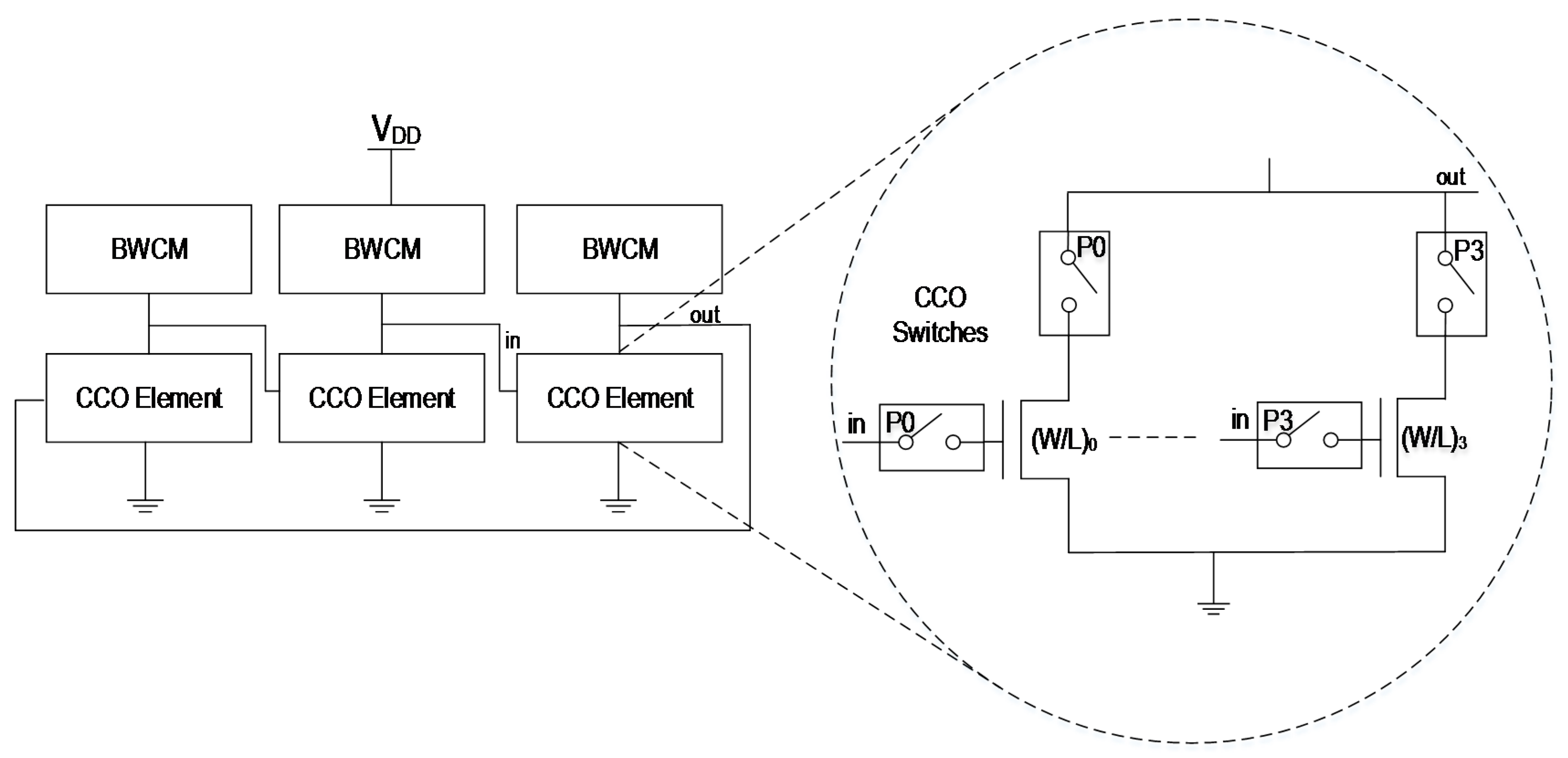
vs. temperature curve. Therefore, the drive strength of the NMOS devices is also required to be controlled using process trimming bits in addition to extending the BWCM current range. The CCO elements for different process corners are switched using CCO switches as shown in Figure 10. Process-trimming bits P<3:0> are used to enable different drive strengths of the CCO NMOS element ((W/L)1 through (W/L)4). A smaller (W/L) ratio provides sufficient drive current in a faster corner, whereas, a larger (W/L) ratio is required in slower process corners to provide sufficient drive strength of the CCO. From Monte Carlo simulations and trimming data points, it was chosen to have four CCO branches controlled by bits P<3:0>. Having many CCO parallel branches will not increase accuracy, because a higher number of “off” CCO branches increases the leakage current and affects the linearity. In case of BWCM bits (B<7:0>), multiple branches can be “on” at the same time and that happens when set automatically using the locking circuit. However, only one of the four CCO branches are set to be “on” at a time for different drive strengths; therefore, P<3:0> is a one-hot code.
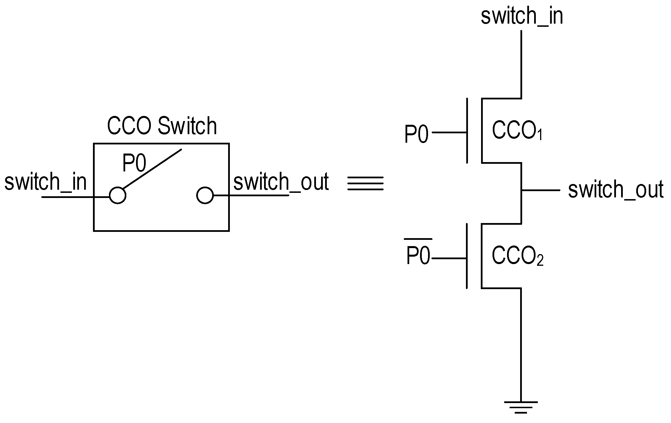
The CCO switches are shown in Figure 11. When P0 is 1, the corresponding CCO branch is enabled. The top device CCO1 is sized to allow the entire current IBWCM to the corresponding CCO elements. When P0 is 0, the corresponding CCO branch is disabled. The bottom device CCO2 pulls down the VDS and VGS to ground to effectively turn off the CCO NMOS element. When a branch is disabled, there is leakage current through these devices, but it is sufficiently low to maintain the linearity of the mirrored BWCM current.
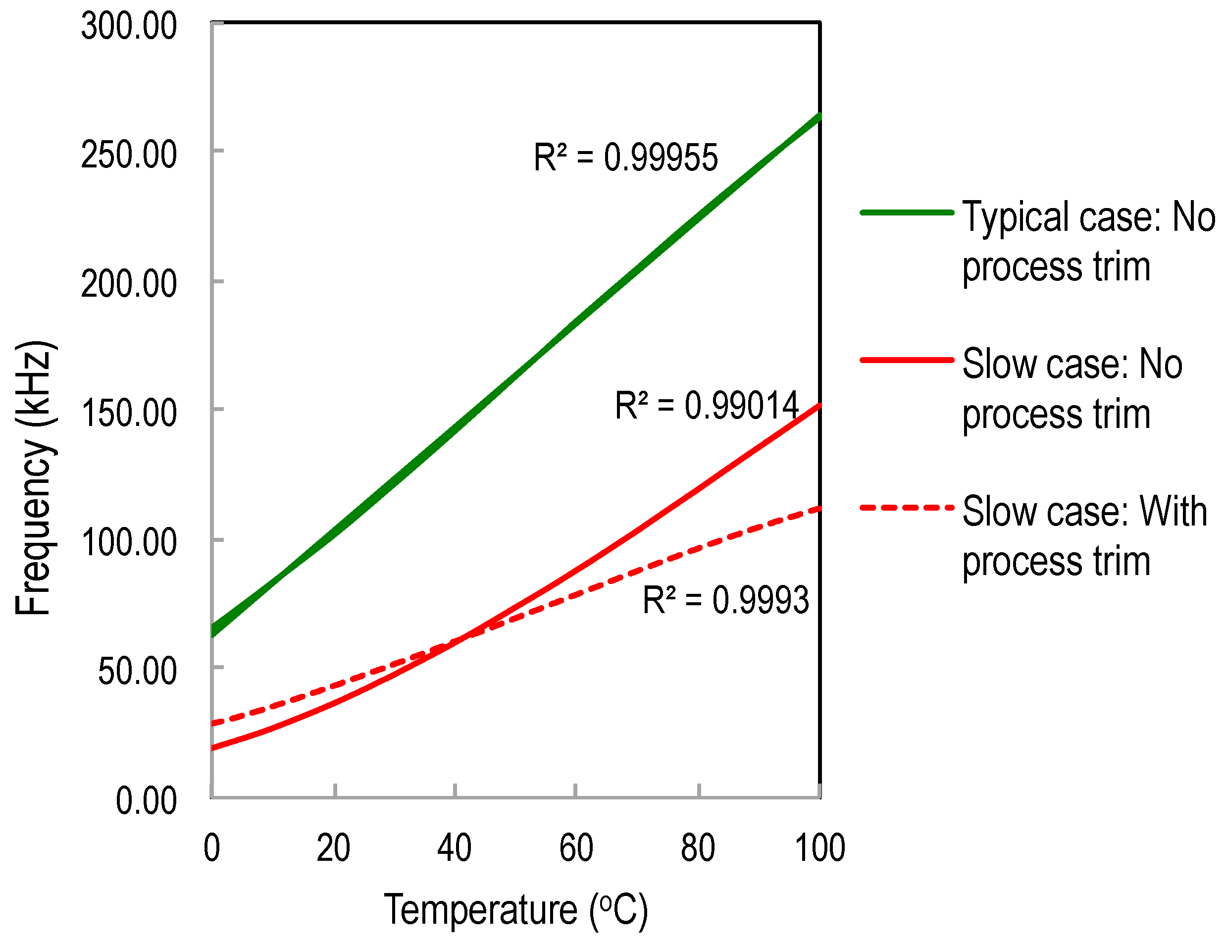
Figure 12 shows the effect of process trimming of CCO elements. It is to be noted that for this experiment, 100% of the PTAT current is mirrored (B<7:0> = 1000 0000) without accounting for power savings. For typical case of process variations, the linearity is high (R2 = 0.99955) with the default CCO device strength (P0 = 0). We demonstrate the effect for a slower case of process variations, in which the CCO element needs to be trimmed to improve the drive strength. With process trimming, an improvement in R2 value (from R2 = 0.99014 to R2 = 0.9993) is observed as shown in Figure 12. Process bits can, therefore, be used to trim the devices in different process corners.
The BWCM bits B<7:0> and process bits P<3:0> are set during the initial calibration phase. The process bits are first manually configured by setting B<7:0> to 1000 0000 to mirror 100% of the PTAT current. The final BWCM scaling is performed after process trimming. This is because, when the CCO NMOS strength is sufficient for 100% PTAT current, it will be sufficient for the scaled current as well. In simulations, the PTAT current gives an idea of the process and P<3:0> was set accordingly. In real chip implementations, on-chip process monitors give the idea of the process.
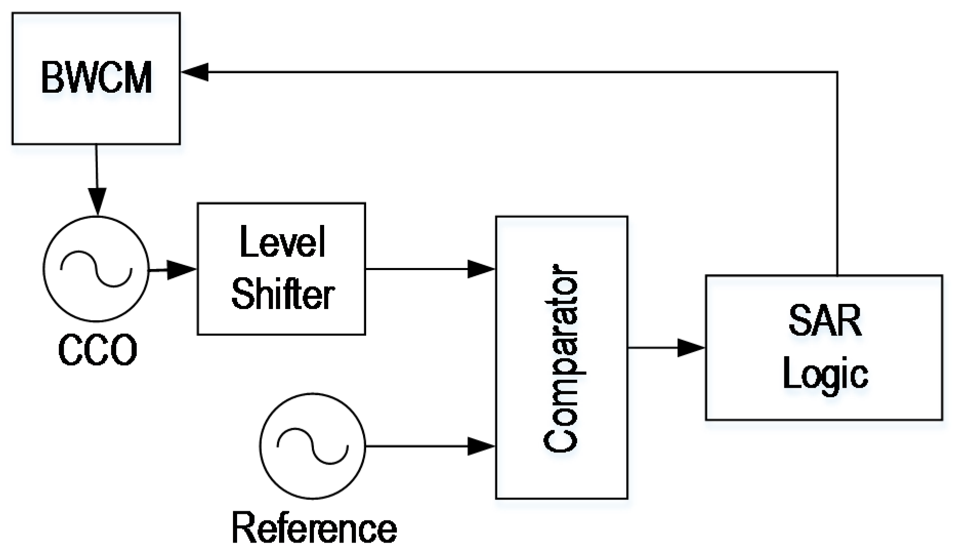
Secondly, the BWCM bits may be manually or otherwise automatically set using a locking circuit [11] as shown in Figure 13. The CCO output frequency is representative of the amount of IBWCM that is starving the CCO NMOS devices. This information can be used as a feedback to control the current that is mirrored from the PTAT to the CCO stages during calibration. The locking circuit shown in Figure 13 can be used to lock the CCO frequency to a reference clock, which may be derived directly from the system clock or it can be a fraction of the system clock. The BWCM bits B<7:0> are then set by the locking circuit to automatically control the power consumption of the temperature sensor system. The locking circuit is operational using the digital logic supply voltage of 0.5 V.
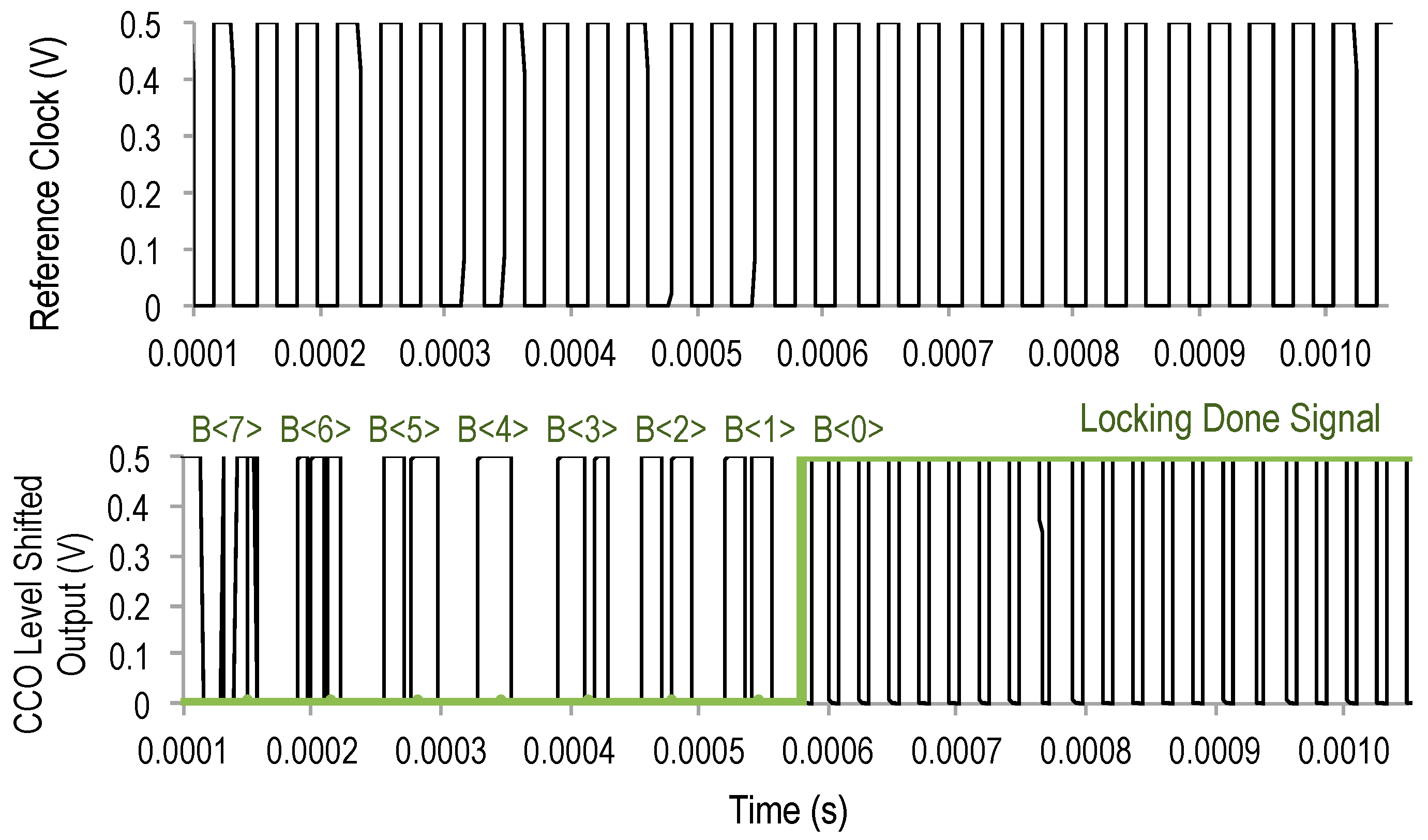
Figure 14 shows the locking mechanism. In this example, the reference clock is assumed to be derived from the system crystal oscillator clock and its frequency is set to be approximately that of a crystal at 33 kHz. The bits B<7:0> are set one after the other by the SAR logic in the locking circuit to lock the CCO to a frequency comparable to the reference frequency at 39 kHz. The locked frequency does not closely match the reference frequency with high accuracy, unlike the clock source in which the locking circuit was used [11], because the granularity of the current sources in this design is not sufficient to achieve small delays for high accuracy locking. However, this level of proximity to the reference frequency is sufficient for our purpose of power reduction in a temperature sensor. The value of B<7:0> for the lock shown in Figure 14 is 0001 1100. The optimal reference frequency range for different process corners is to be carefully chosen because choosing a higher frequency does not achieve power savings, whereas choosing too low a frequency lowers the BWCM current drastically to affect its linearity as leakage currents become dominant.
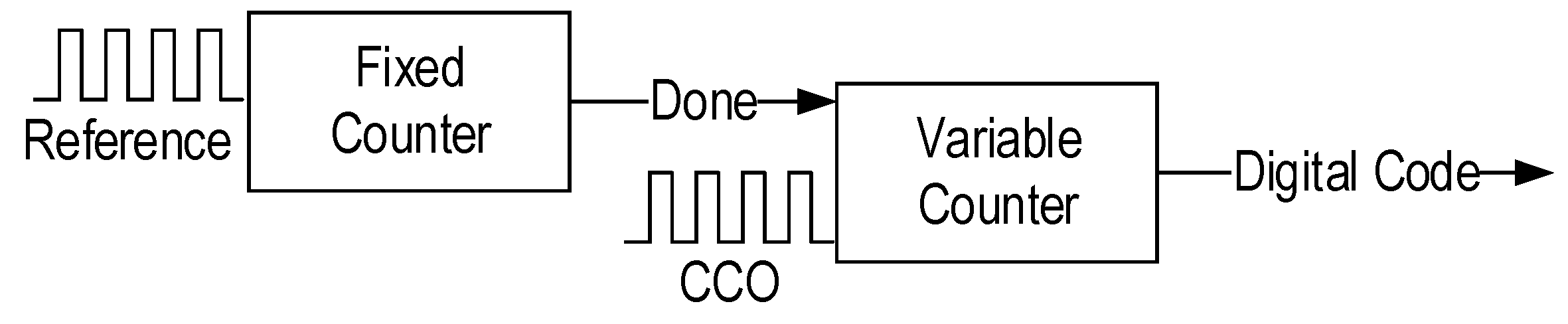
2.4. Digital Block

The digital block has a programmable fixed and a variable counter synthesized using low leakage high-VT logic as shown in Figure 15. The fixed counter asserts a Done signal after counting a preset number of reference clock (e.g., system clock) cycles. This gives a fixed time window for temperature sampling and conversion into digital code. The variable counter counts the CCO cycles until Done is asserted high and outputs a code that is representative of the CCO frequency and, therefore, the ambient temperature. Prior to the next temperature fetch, both of the counters are reset.

3. Simulation Results

3.1. PTAT Output Current vs. Temperature

Figure 16 shows a 100-point Monte Carlo simulation plot of PTAT current IOUT vs. temperature from 0 °C to 100 °C. We observe that the PTAT current is linear across different iterations. The linearity of PTAT current is denoted by R2 (measure of goodness of fit in linear regressions). The linearity histogram for a 100-point Monte Carlo simulation is shown in Figure 17. The mean R2 of the PTAT current is 0.9993 and the 3σ variation is 0.0024, which indicates high linearity.

3.2. Bit-Weighted Current Mirror Configuration

The PTAT current is mirrored to starve the CCO using a BWCM. Figure 18 demonstrates the advantage of using a BWCM. In fast process corners, such as FF, the PTAT current is higher than desired and, when mirrored to subsequent CCO stages, this causes higher power consumption than desired. Figure 18 shows the cases when 100% of the PTAT current is mirrored. For fast process corners, only a fraction of the PTAT current is required to be mirrored to control the power consumption of the temperature sensor system. Figure 18 also shows the scaled BWCM current (50% and 25% PTAT) for different bit-configurations of B<7:0> for fast process corners. When the scaled current is mirrored to the subsequent CCO stages, it enables control of the power consumption of the temperature sensor system.

3.3. CCO Frequency (Untrimmed) vs. Temperature

The frequency vs. temperature curves for a 100-point Monte Carlo run without process trimming of the CCO NMOS devices are shown in Figure 19. We observe non-linearity in some of the curves because they belong to slower process corners where the drive strength of the CCO is insufficient or to faster process corners in which the non-linear leakage current becomes a comparable component in the starving current. The actual inaccuracies are determined in the following section in which the CCO is process trimmed according the process corner.

3.4. Inaccuracy vs. Temperature, Supply Noise Sensitivity, and Power Consumption

To measure inaccuracy it is required to calibrate the CCO pull-down to control the drive strength. The calibration was done for 15 points of the Monte Carlo simulations from Section 3.3. To measure the inaccuracy, a two-point temperature calibration is done at 10 °C and 80 °C. A straight line joining these calibration points gives the required frequency vs. temperature extrapolation line. The inaccuracy is determined from the deviation of the actual frequency vs. temperature curve from the straight line after calibration. Figure 20 shows the histogram of the temperature sensor inaccuracy of the 15 data points taken from the 100 Monte Carlo simulation points and inaccuracy was determined after process trimming of the CCO delay elements. The mean inaccuracy is +1.0/−1.2 °C and maximum inaccuracy is +1.5/−1.7 °C for the 15 process trimmed data points. The frequency range of the CCO gives a resolution of 0.008 °C/LSB, although the thermal noise floor limits the practical resolution. Programmable counters enable different sampling windows for temperature conversion, making the resolution-power trade-off possible.
A variation of the power supply because of variation of the reference voltage due to temperature will add additional inaccuracy in the temperature sensor. This supply noise variation was simulated to be 0.032 °C/mV. It can be improved using decoupling capacitors (~20 pF of area ~50 × 50 μm2). To effectively eliminate the effect of supply noise that is 1 kHz or higher, a low-pass filter (off-chip 50 kΩ and 10 nF) can be used. The sensor presents a low load, so it can be operated from a well-controlled supply using an LDO too.
To measure the power consumption, the BWCM bit value for typical case was set to 1000 0000. For faster process corners the bits were set to scale the current accordingly while maintaining high linearity of the mirrored current. The average power consumption of the analog core at 0.2 V is 18 nW. The total system power (including the locking circuit, level shifter [12] and digital block at 0.5 V) is 23 nW. A lower sampling rate further saves power as the digital blocks consume only 190 pW of leakage between samples.

4. Comparison with Prior Art

Table 1 compares the proposed temperature sensor design with other recent low-power designs of varying circuit topologies with sub-µW power consumption. This work focuses on lowering the power consumption while maintaining a similar inaccuracy and temperature range compared to prior art. Compared to a recent ULP temperature sensor [9], the proposed temperature sensor system has 3× lower power and comparable inaccuracy.

5. Conclusions

The proposed ULP sub-VT temperature sensor core is operational down to 0.2 V. Together with digital logic at 0.5 V, the total system power consumption is 23 nW, and the maximum inaccuracy is +1.5/−1.7 °C in the temperature range of 0 °C to 100 °C with a two-point calibration. A bit-weighted current mirror architecture resists process-induced power variations, process trimming bits in the current-controlled oscillator control its drive strength, and a programmable digital control based on counters supports a resolution-power trade-off for IoT applications with different sampling rate and energy needs. The area of the analog core is 150 × 100 μm2 and the total system area is 250 × 250 μm2 as shown in the layout in Figure 21.

Acknowledgments

This work was funded in part by the NSF NERC ASSIST Center (EEC-1160483).

Author Contributions

Divya Akella Kamakshi designed the temperature sensor circuit and performed the simulations described in this paper with guidance from Aatmesh Shrivastava and Benton H. Calhoun. Aatmesh Shrivastava contributed to the design and the theoretical analysis in the paper. The manuscript was written by Divya Akella Kamakshi with contributions in both technical and formatting aspects from Aatmesh Shrivastava and Benton H. Calhoun.

Conflicts of Interest

The authors declare no conflict of interest. The founding sponsors had no role in the design of the study; in the collection, analyses, or interpretation of data; in the writing of the manuscript, and in the decision to publish the results.

References

  1. Shrivastava, A.; Roberts, N.E.; Khan, O.U.; Wentzloff, D.D.; Calhoun, B.H. A 10 mV-Input Boost Converter with Inductor Peak Current Control and Zero Detection for Thermoelectric and Solar Energy Harvesting with 220 mV Cold-Start and −14.5 dBm, 915 MHz RF Kick-Start. IEEE J. Solid-State Circuits 2015, 50, 1820–1832. [Google Scholar] [CrossRef]
  2. Zhang, F.; Miyahara, Y.; Otis, B.P. Design of a 300-mV 2.4-GHz Receiver Using Transformer-Coupled Techniques. IEEE J. Solid-State Circuits 2013, 48, 3190–3205. [Google Scholar] [CrossRef]
  3. Shrivastava, A.; Akella Kamakshi, D.; Calhoun, B.H. A 1.5 nW, 32.768 kHz XTAL Oscillator Operational From a 0.3 V Supply. IEEE J. Solid-State Circuits 2016, 51, 686–696. [Google Scholar]
  4. Klinefelter, A.; Roberts, N.E.; Shakhsheer, Y.; Gonzalez, P.; Shrivastava, A.; Roy, A.; Craig, K.; Faisal, M.; Boley, J.; Oh, S.; et al. A 6.45 μW Self-Powered IoT SoC with Integrated Energy-Harvesting Power Management and ULP Asymmetric Radios. IEEE Trans. Biomed. Circuits Syst. 2015, 9, 862–874. [Google Scholar]
  5. Souri, K.; Chae, Y.; Makinwa, K. A CMOS temperature sensor with a voltage-calibrated inaccuracy of ±0.15 °C (3σ) from −55 to 125 °C. In Proceedings of the 2012 IEEE International Solid-State Circuits Conference Digest of Technical Papers (ISSCC), San Francisco, CA, USA, 19–23 February 2012; pp. 208–210.
  6. Souri, K.; Chae, Y.; Thus, F.; Makinwa, K. 12.7 A 0.85 V 600 nW all-CMOS temperature sensor with an inaccuracy of ±0.4 °C (3 sigma) from −40 to 125 °C. In Proceedings of the 2014 IEEE International Solid-State Circuits Conference Digest of Technical Papers (ISSCC), San Francisco, CA, USA, 9–13 February 2014; pp. 222–223.
  7. Lin, Y.; Sylvester, D.; Blaauw, D. An ultra low power 1 V, 220 nW temperature sensor for passive wireless applications. In Proceedings of the 2008 IEEE Custom Integrated Circuits Conference, San Jose, CA, USA, 21–24 September 2008; pp. 507–510.
  8. Law, M.K.; Bermak, A.; Luong, H.C. A Sub-μW Embedded CMOS Temperature Sensor for RFID Food Monitoring Application. IEEE J. Solid-State Circuits 2010, 45, 1246–1255. [Google Scholar] [CrossRef]
  9. Jeong, S.; Foo, Z.; Lee, Y.; Sim, J.; Blaauw, D.; Sylvester, D. A Fully-Integrated 71 nW CMOS Temperature Sensor for Low Power Wireless Sensor Nodes. IEEE J. Solid-State Circuits 2014, 49, 1682–1693. [Google Scholar] [CrossRef]
  10. Kamakshi, D.A.; Shrivastava, A.; Calhoun, B.H. A 23 nW CMOS ultra-low power temperature sensor operational from 0.2 V. In Proceedings of the SOI-3D-Subthreshold Microelectronics Technology Unified Conference (S3S), Rohnert Park, CA, USA, 5–8 October 2015; pp. 1–3.
  11. Shrivastava, A.; Calhoun, B.H. A 150 nW, 5 ppm/°C, 100 kHz On-Chip clock source for ultra low power SoCs. In Proceedings of the 2012 IEEE Custom Integrated Circuits Conference (CICC), San Jose, CA, USA, 9–12 September 2012; pp. 1–4.
  12. Luo, S.; Huang, C.; Chu, Y. A Wide-Range Level Shifter Using a Modified Wilson Current Mirror Hybrid Buffer. IEEE Trans. Circuits Syst. I Regul. Pap. 2014, 61, 1656–1665. [Google Scholar] [CrossRef]
  13. Law, M.K.; Bermak, A. A 405-nW CMOS Temperature Sensor Based on Linear MOS Operation. IEEE Trans. Circuits Syst. II Express Briefs 2009, 56, 891–895. [Google Scholar] [CrossRef]
Figure 1. A simplified block diagram of the proposed temperature sensor system.
Jlpea 06 00010 g001
Figure 2. Temperature sensor system [10]: it consists of a sub-VT PTAT current source, a bit-weighted current mirror, a current controlled oscillator and a digital block. (Based on “A 23 nW CMOS Ultra-Low Power Temperature Sensor Operational from 0.2 V”, by Divya Akella Kamakshi, Aatmesh Shrivastava, and Benton H. Calhoun, which appeared in SOI-3D-Subthreshold Microelectronics Technology Unified Conference (S3S), 2015 IEEE, Rohnert Park, CA, USA, 2015, pp. 1–3. © (2015) IEEE.).
Jlpea 06 00010 g002
Figure 3. Sub-VT PTAT current source operational at 0.2 V VDD [10]: the transistors M1 to M4 are operated in the sub-VT saturation region using thin-oxide standard-VT (SVT) devices. (Based on “A 23 nW CMOS Ultra-Low Power Temperature Sensor Operational from 0.2 V”, by Divya Akella Kamakshi, Aatmesh Shrivastava, and Benton H. Calhoun, which appeared in SOI-3D-Subthreshold Microelectronics Technology Unified Conference (S3S), 2015 IEEE, Rohnert Park, CA, USA, 2015, pp. 1–3. © (2015) IEEE.).
Jlpea 06 00010 g003
Figure 4. PTAT current at 27 °C in 100-point Monte-Carlo runs [10]: process variations cause variations in the PTAT current. Mean current = 39 nA; 3σ = 25 nA. (Based on “A 23 nW CMOS Ultra-Low Power Temperature Sensor Operational from 0.2 V”, by Divya Akella Kamakshi, Aatmesh Shrivastava, and Benton H. Calhoun, which appeared in SOI-3D-Subthreshold Microelectronics Technology Unified Conference (S3S), 2015 IEEE, Rohnert Park, CA, USA, 2015, pp. 1–3. © (2015) IEEE.).
Jlpea 06 00010 g004
Figure 5. PTAT current is mirrored using a BWCM to control the current starving the CCO [10]. (Based on “A 23 nW CMOS Ultra-Low Power Temperature Sensor Operational from 0.2 V”, by Divya Akella Kamakshi, Aatmesh Shrivastava, and Benton H. Calhoun, which appeared in SOI-3D-Subthreshold Microelectronics Technology Unified Conference (S3S), 2015 IEEE, Rohnert Park, CA, USA, 2015, pp. 1–3. © (2015) IEEE.).
Jlpea 06 00010 g005
Figure 6. Bit-weighted current mirror circuit (BWCM). (Based on “A 23 nW CMOS Ultra-Low Power Temperature Sensor Operational from 0.2 V”, by Divya Akella Kamakshi, Aatmesh Shrivastava, and Benton H. Calhoun, which appeared in SOI-3D-Subthreshold Microelectronics Technology Unified Conference (S3S), 2015 IEEE, Rohnert Park, CA, USA, 2015, pp. 1–3. © (2015) IEEE.).
Jlpea 06 00010 g006
Figure 7. Architecture of the BWCM switch to enable or disable the BWCM arms [10]. (Based on “A 23 nW CMOS Ultra-Low Power Temperature Sensor Operational from 0.2 V”, by Divya Akella Kamakshi, Aatmesh Shrivastava, and Benton H. Calhoun, which appeared in SOI-3D-Subthreshold Microelectronics Technology Unified Conference (S3S), 2015 IEEE, Rohnert Park, CA, USA, 2015, pp. 1–3. © (2015) IEEE.).
Jlpea 06 00010 g007
Figure 8. (a) When a current mirror branch is disabled by pulling PMOS to only 0.2 V VDD, it is not effectively turned off and its leakage contributes to the BWCM current causing non-linearity in the BWCM current vs. temperature curve (R2 = 0.9753) [10]; and (b) the disabled BWCM current mirror branch is turned off by tying the PMOS gate to 0.5 V VDDH. This reduces the PMOS leakage and enables a highly linear BWCM current vs. temperature performance (R2 = 0.9997) [10]. (Based on “A 23 nW CMOS Ultra-Low Power Temperature Sensor Operational from 0.2 V”, by Divya Akella Kamakshi, Aatmesh Shrivastava, and Benton H. Calhoun, which appeared in SOI-3D-Subthreshold Microelectronics Technology Unified Conference (S3S), 2015 IEEE, Rohnert Park, CA, USA, 2015, pp. 1–3. © (2015) IEEE.).
Jlpea 06 00010 g008
Figure 9. NMOS-only CCO in which the frequency is determined by IBWCM and capacitors CL [10]. (Based on “A 23 nW CMOS Ultra-Low Power Temperature Sensor Operational from 0.2 V”, by Divya Akella Kamakshi, Aatmesh Shrivastava, and Benton H. Calhoun, which appeared in SOI-3D-Subthreshold Microelectronics Technology Unified Conference (S3S), 2015 IEEE, Rohnert Park, CA, USA, 2015, pp. 1–3. © (2015) IEEE.).
Jlpea 06 00010 g009
Figure 10. Process trimming to tune the drive strength of CCO devices.
Jlpea 06 00010 g010
Figure 11. CCO switch architecture.
Jlpea 06 00010 g011
Figure 12. Effect of process trimming: the design shows high linearity (R2 = 0.9995) for typical case. For slower process corners, the drive strength of the CCO NMOS element has to be controlled using process bits. With process trimming the R2 improves from 0.99014 to 0.9993.
Jlpea 06 00010 g012
Figure 13. Locking circuit [11] to automatically set BWCM bits B<7:0>.
Jlpea 06 00010 g013
Figure 14. Locking CCO to a reference clock.
Jlpea 06 00010 g014
Figure 15. Digital block consisting of two counters to convert temperature to digital code.
Jlpea 06 00010 g015
Figure 16. 100 point Monte Carlo plot of PTAT output current IOUT vs. temperature.
Jlpea 06 00010 g016
Figure 17. Linearity histogram of PTAT current: mean R2 value = 0.9993; 3σ R2 = 0.0024 [10]. (Based on “A 23 nW CMOS Ultra-Low Power Temperature Sensor Operational from 0.2 V”, by Divya Akella Kamakshi, Aatmesh Shrivastava, and Benton H. Calhoun, which appeared in SOI-3D-Subthreshold Microelectronics Technology Unified Conference (S3S), 2015 IEEE, Rohnert Park, CA, USA, 2015, pp. 1–3. © (2015) IEEE.).
Jlpea 06 00010 g017
Figure 18. Different fractions of BWCM current in faster process corners saves power.
Jlpea 06 00010 g018
Figure 19. Frequency vs. temperature curves (100 points) without process trimming [10]. Based on “A 23 nW CMOS Ultra-Low Power Temperature Sensor Operational from 0.2 V”, by Divya Akella Kamakshi, Aatmesh Shrivastava, and Benton H. Calhoun, which appeared in SOI-3D-Subthreshold Microelectronics Technology Unified Conference (S3S), 2015 IEEE, Rohnert Park, CA, USA, 2015, pp. 1–3. © (2015) IEEE.
Jlpea 06 00010 g019
Figure 20. Inaccuracy histogram (15 points) after trimming. The mean inaccuracy is +1.0/−1.2 °C, the maximum inaccuracy is +1.5/−1.7 °C [10]. (Based on “A 23 nW CMOS Ultra-Low Power Temperature Sensor Operational from 0.2 V”, by Divya Akella Kamakshi, Aatmesh Shrivastava, and Benton H. Calhoun, which appeared inSOI-3D-Subthreshold Microelectronics Technology Unified Conference (S3S), 2015 IEEE, Rohnert Park, CA, USA, 2015, pp. 1–3. © (2015) IEEE.).
Jlpea 06 00010 g020
Figure 21. Temperature sensor layout [10]. (Based on “A 23 nW CMOS Ultra-Low Power Temperature Sensor Operational from 0.2 V”, by Divya Akella Kamakshi, Aatmesh Shrivastava, and Benton H. Calhoun, which appeared in SOI-3D-Subthreshold Microelectronics Technology Unified Conference (S3S), 2015 IEEE, Rohnert Park, CA, USA, 2015, pp. 1–3. © (2015) IEEE.).
Jlpea 06 00010 g021
Table 1. Comparison with prior art.
SensorCMOS Technology (μm)VDD (V)Fully IntegratedInaccuracy (°C)Temp. Range (°C)Power (nW)Energy/Conversion (nJ)
This work0.130.2, 0.5Yes1.5/−1.70–100230.23
[6]0.160.85No+/−0.4 (3σ)−40–1256003.6
[7]0.181Yes+3/−1.60–10022022
[8]0.180.5, 1No+1/−0.8−10–301203.6
[9]0.181.2Yes+1.5/−1.40–100712.2
[13]0.181.2No+1/−0.8 0–1004050.41
Based on “A 23 nW CMOS Ultra-Low Power Temperature Sensor Operational from 0.2 V”, by Divya Akella Kamakshi, Aatmesh Shrivastava, and Benton H. Calhoun, which appeared in SOI-3D-Subthreshold Microelectronics Technology Unified Conference (S3S), 2015 IEEE, Rohnert Park, CA, USA, 2015, pp. 1–3. © (2015) IEEE.

