
A Design and Theoretical Analysis of a 145 mV to 1.2 V Single-Ended Level Converter Circuit for Ultra-Low Power Low Voltage ICs †

Abstract
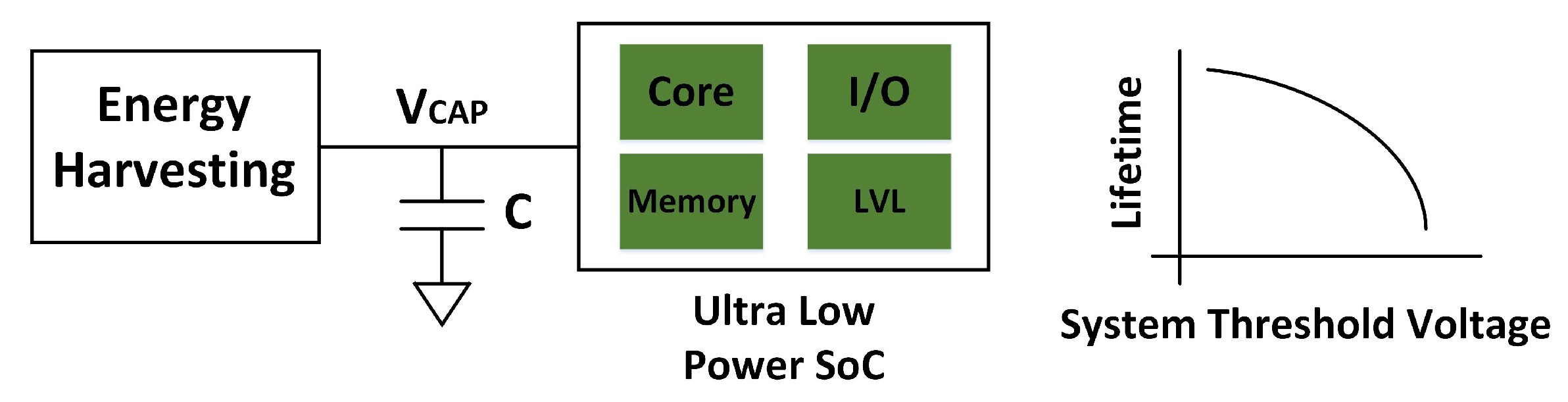
:1. Introduction
2. Level Conversion Techniques
2.1. Amplification-Based Level Conversion
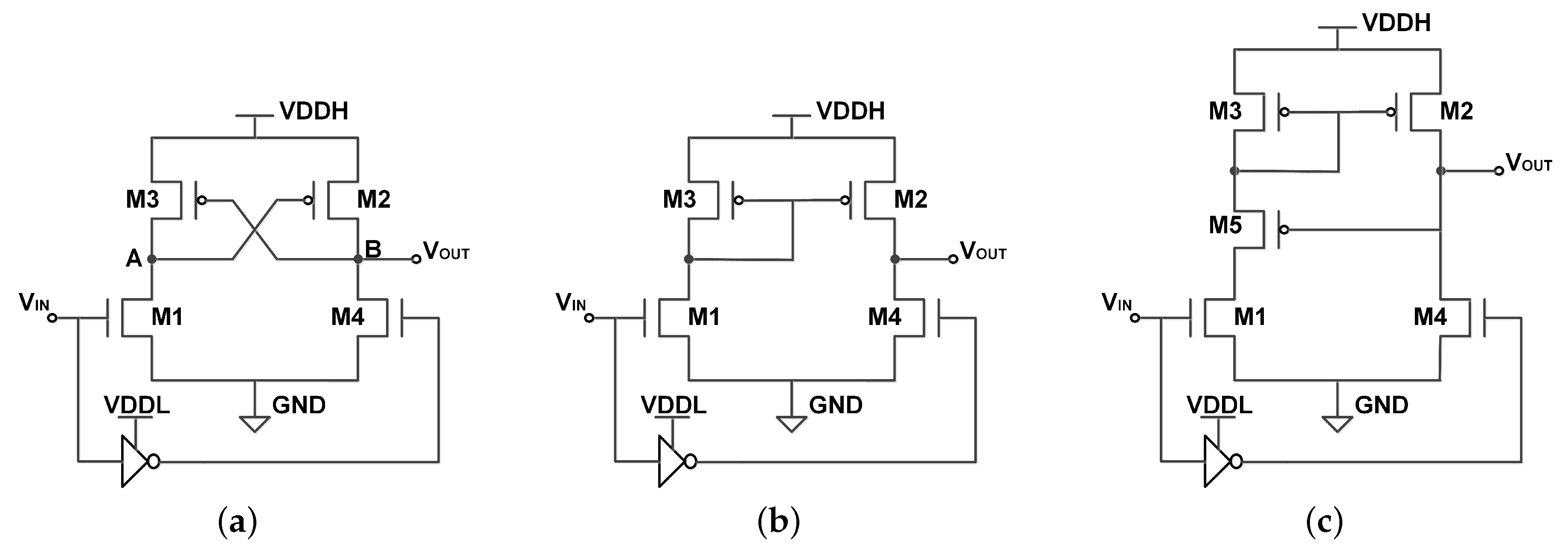
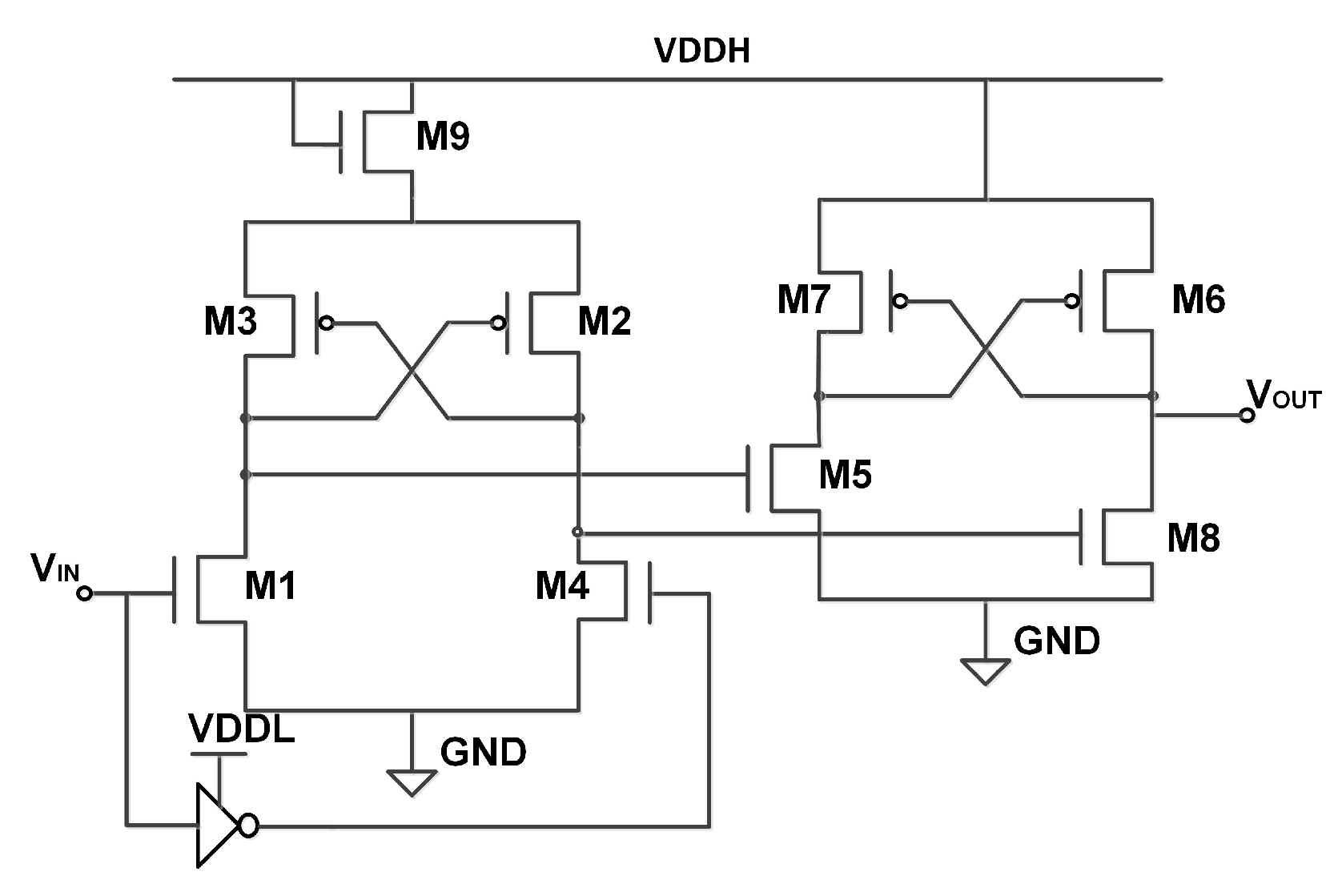
2.1.1. Designs of Amplification-Based Level Converters
2.1.2. Theoretical Analysis of Amplification-Based Level Converters
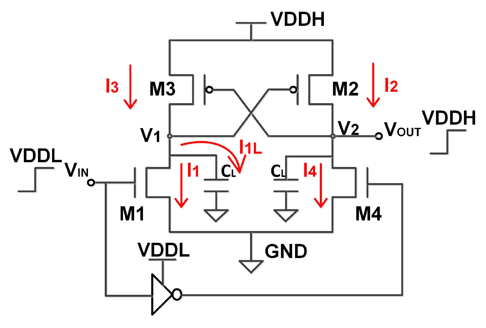
Sufficient Conversion Condition for CCLC
Balanced Switching Condition for CCLC
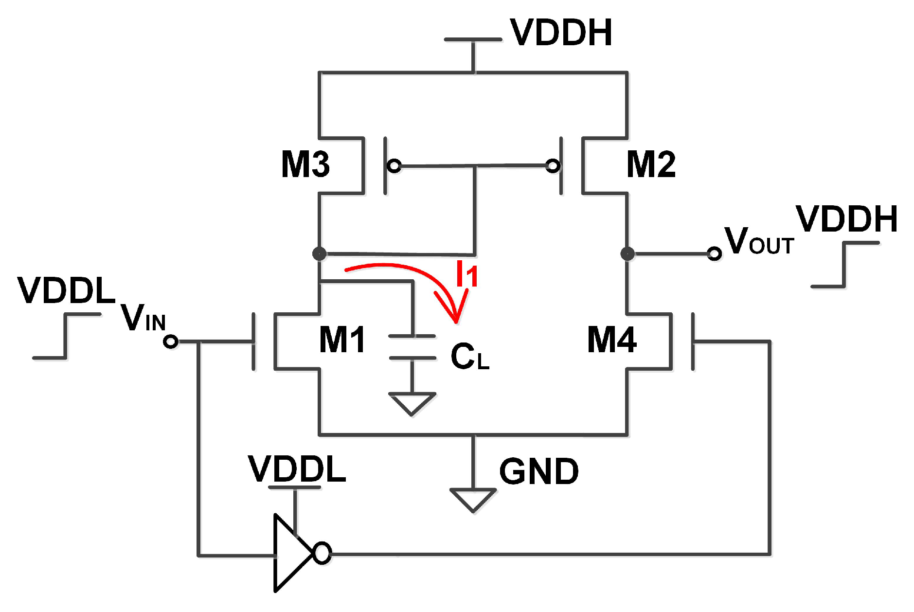
Drawback of CMLC
2.2. Boosted Swing-Based Level Conversion
Designs of Boosted Swing-Based Level Converters
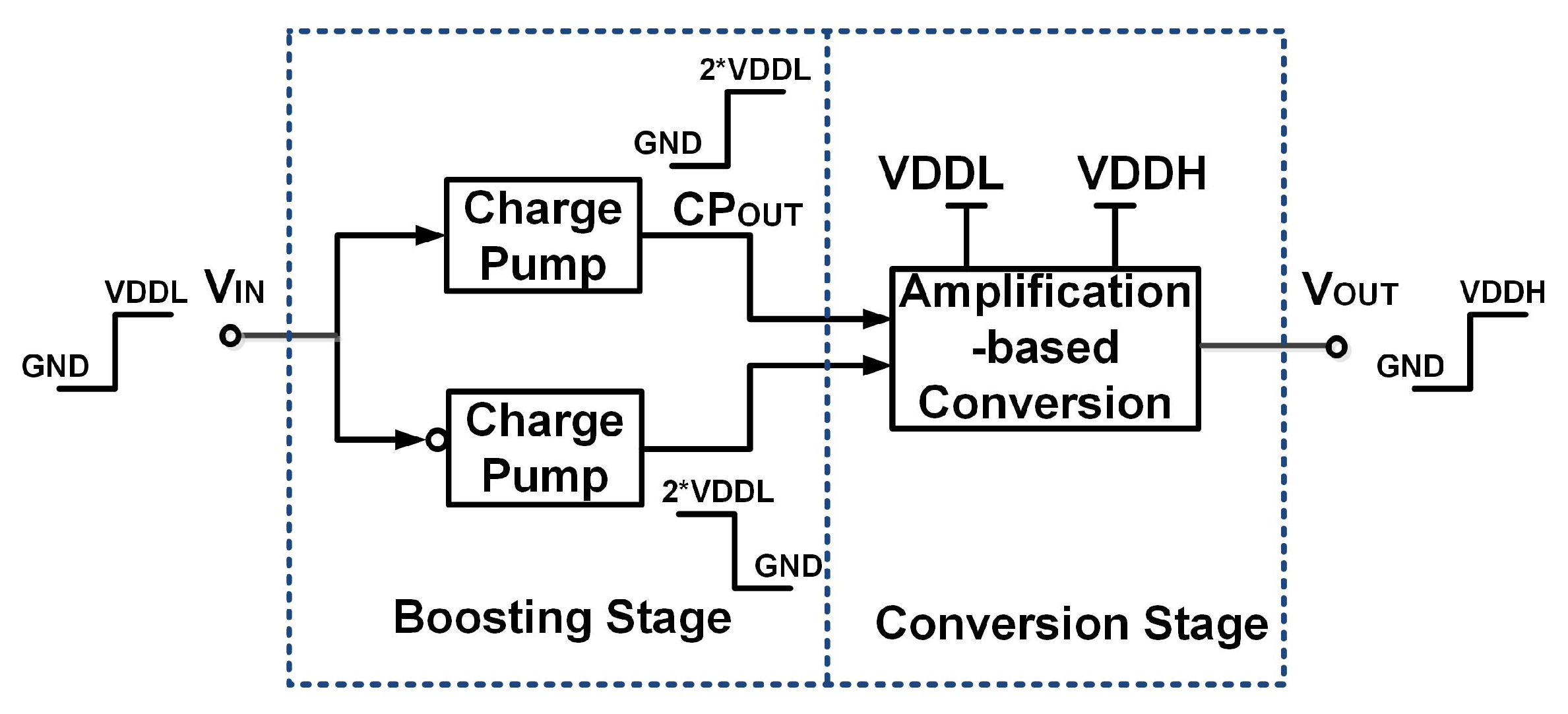
3. Proposed Low Voltage Level Converter
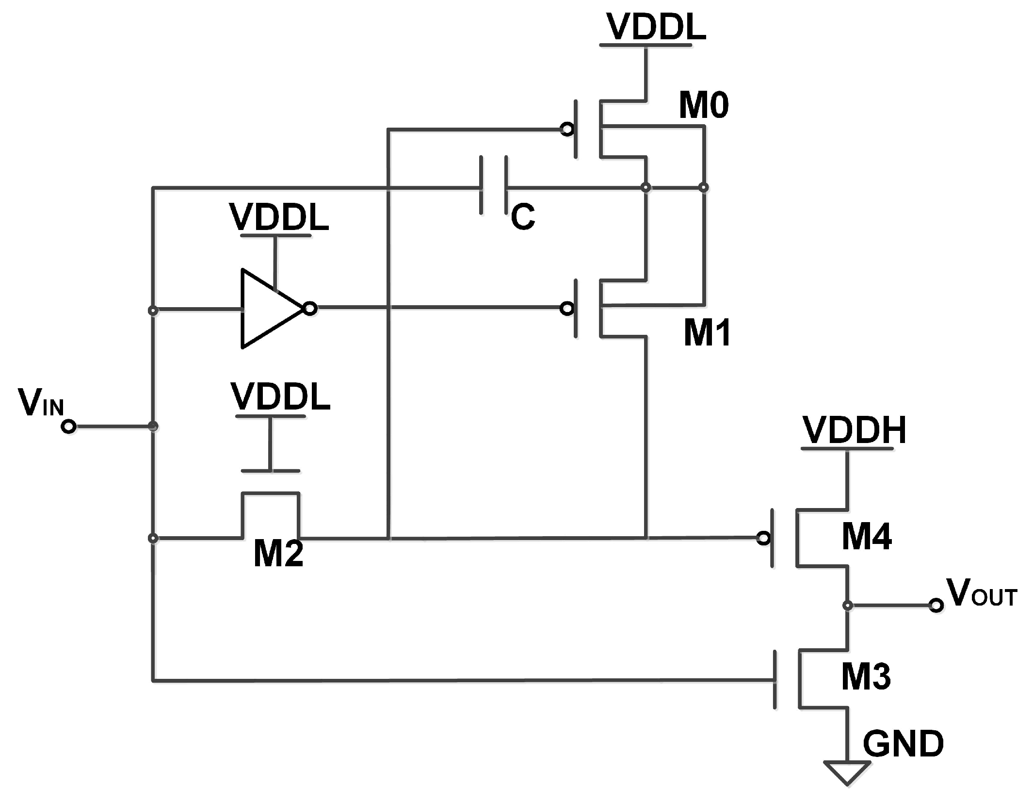
3.1. Subthreshold Charge Pump
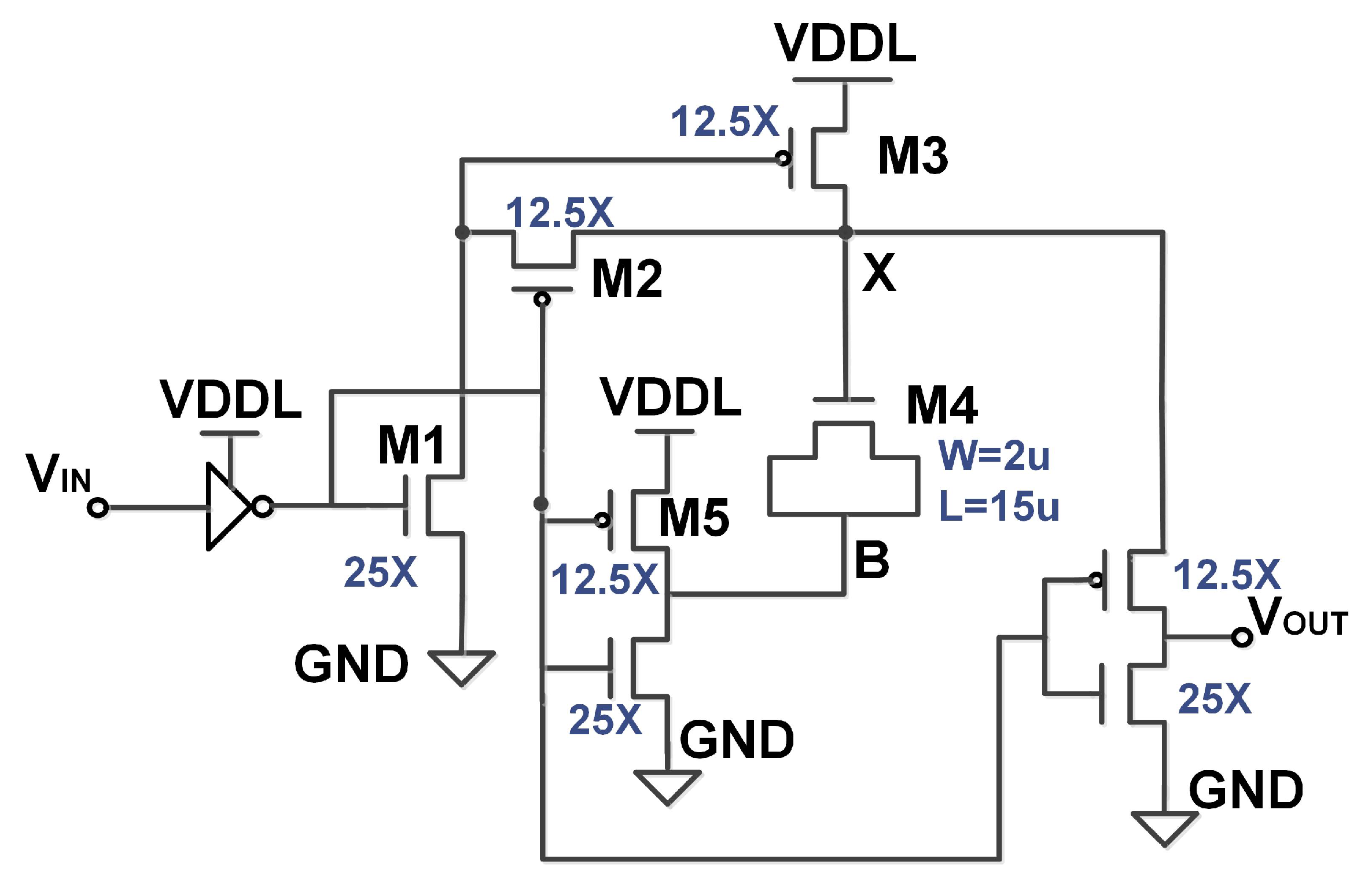
3.2. Implementation of the Proposed Level Converter
Uniform Architecture
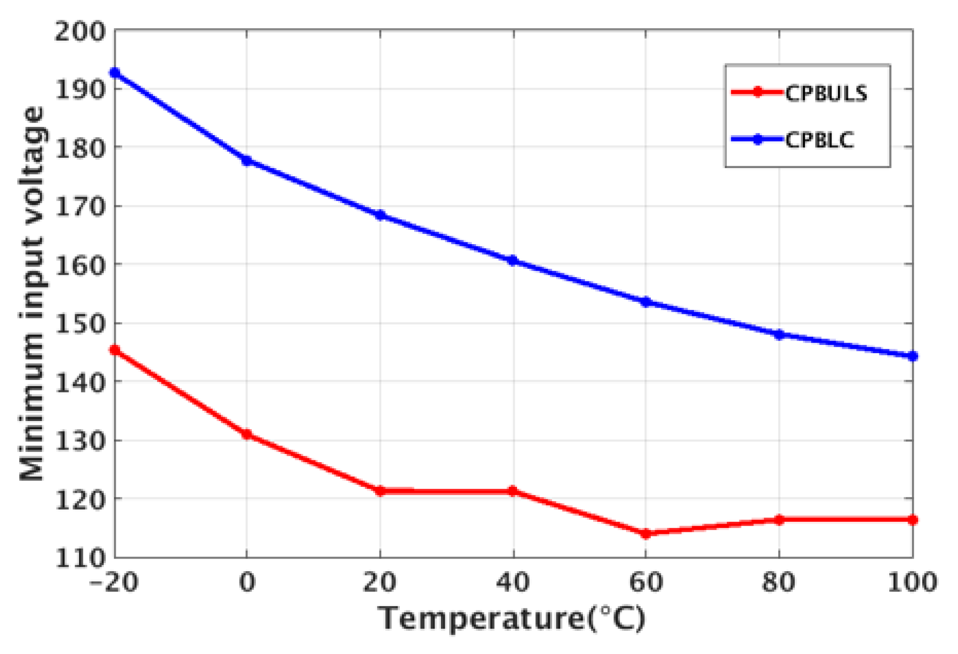
3.3. CPBLC and CPBULS
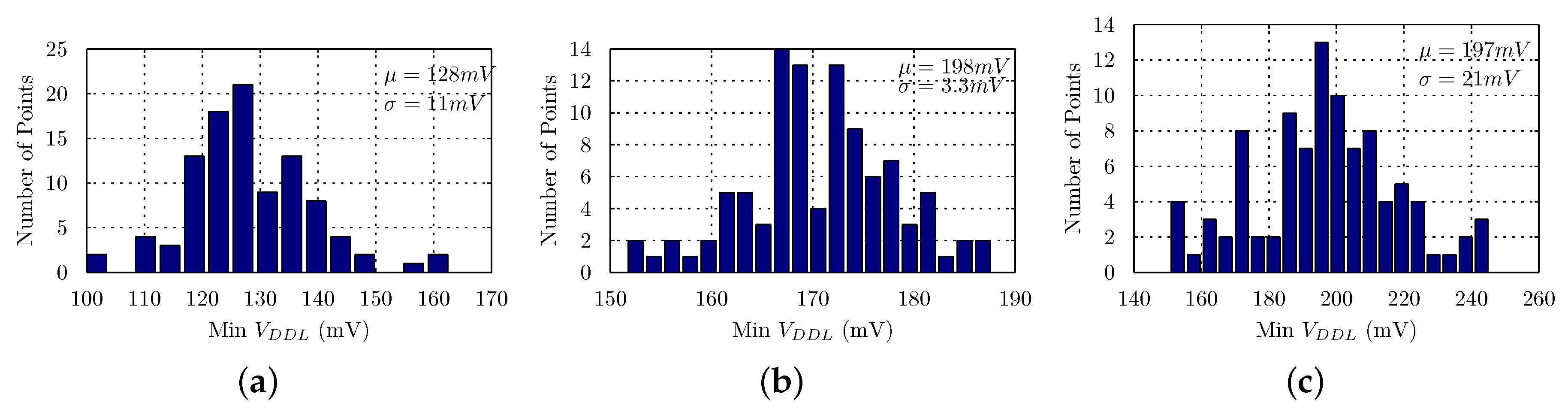
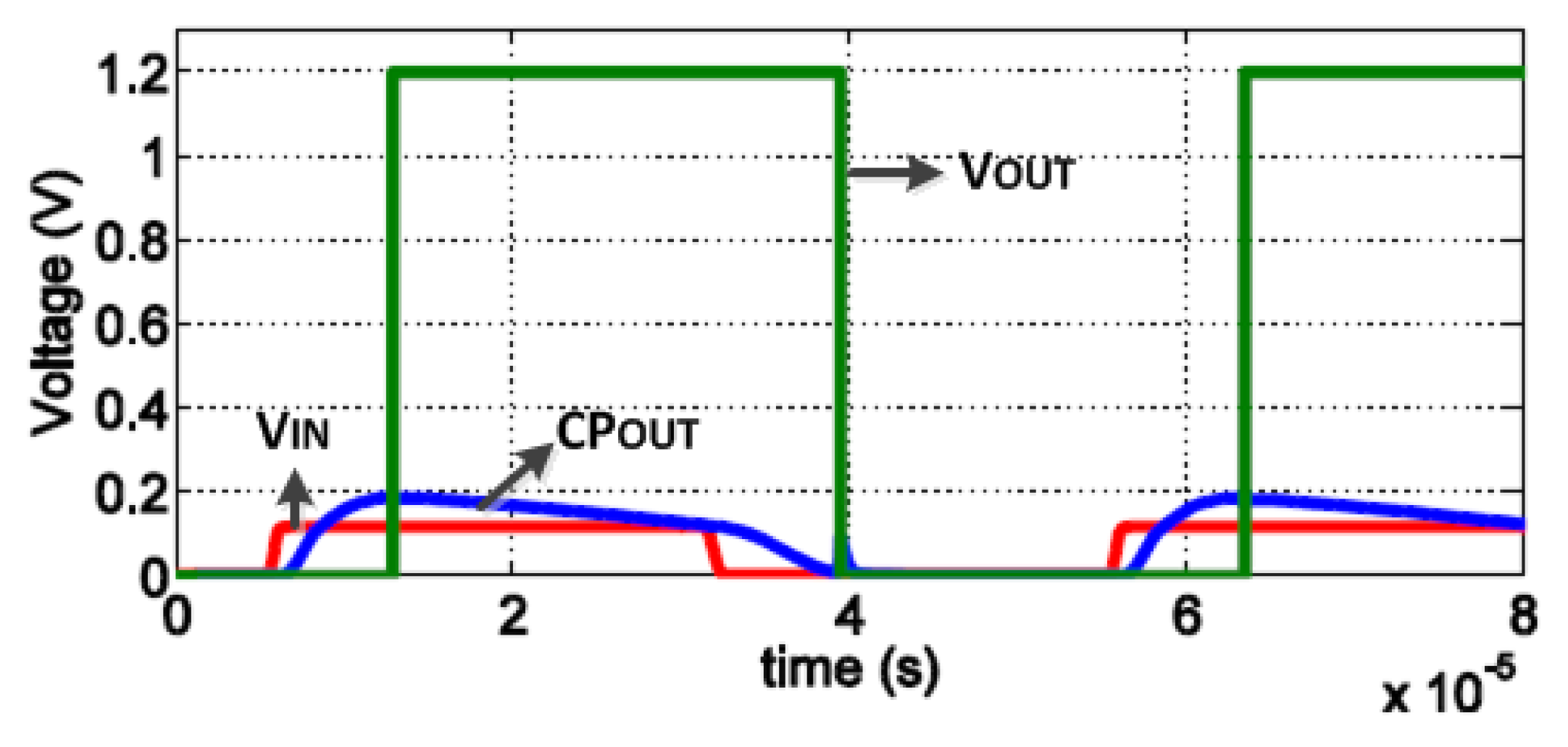
Simulations
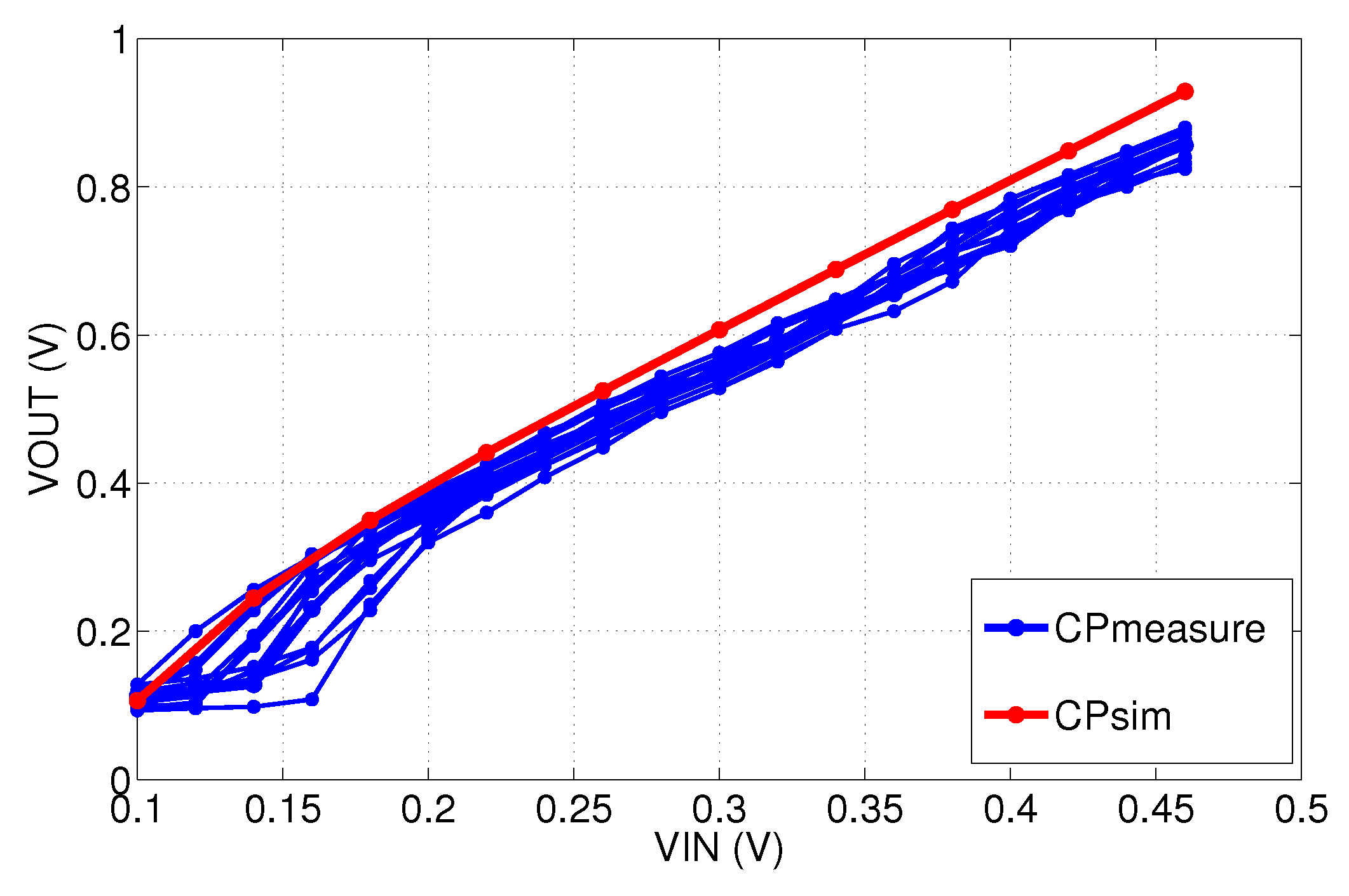
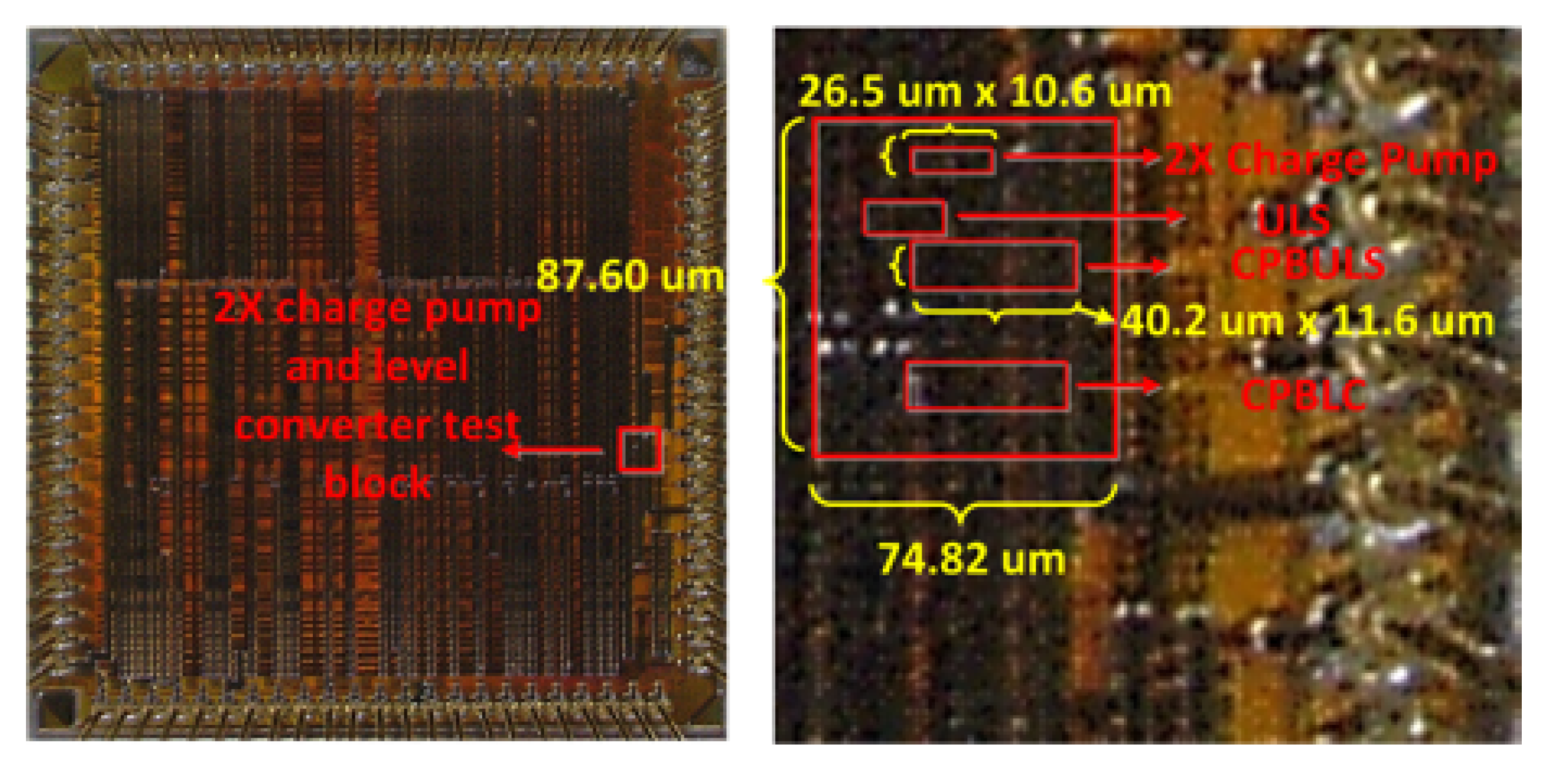
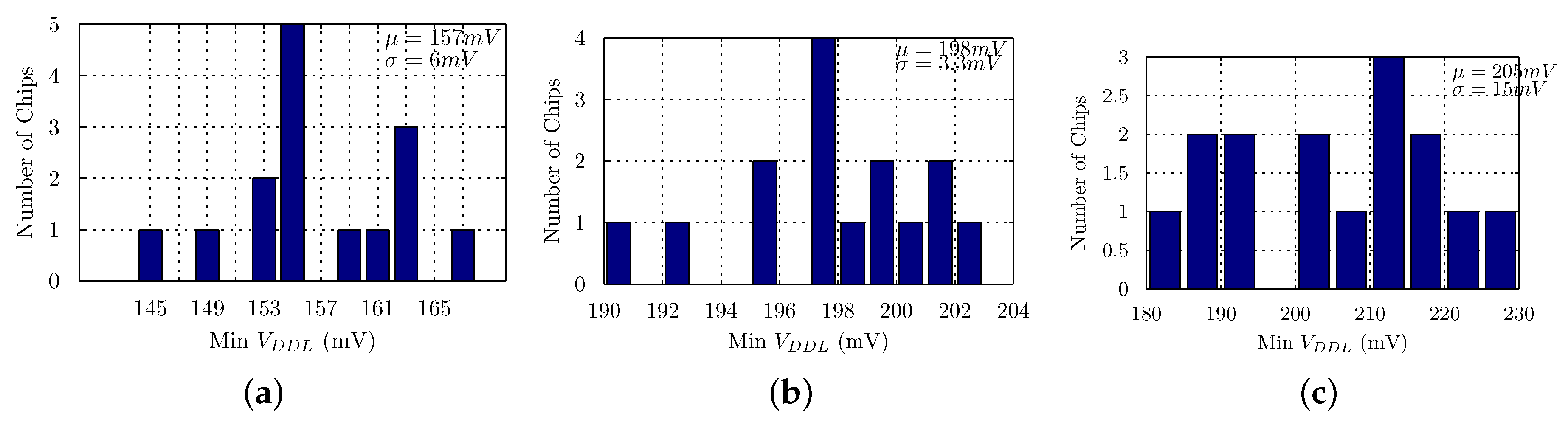
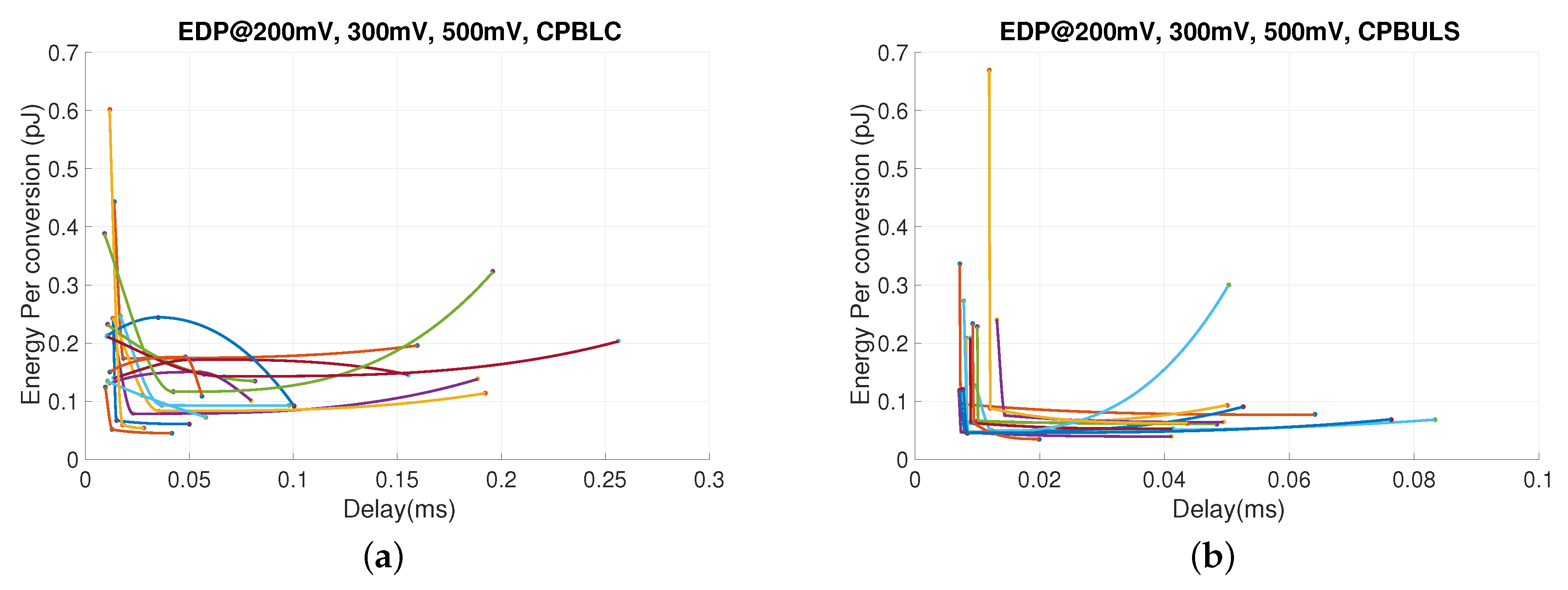
4. Measurements
5. Conclusions
Acknowledgments
Author Contributions
Conflicts of Interest
Abbreviations
| ULP | Ultra low power |
| IoT | Internet of things |
| SoC | System on chip |
| CCLC | Cross-coupled level converter |
| CMLC | Current mirror-based level converter |
| WCMLC | Wilson current mirror level converter |
| PUN | Pull up network |
| PDN | Pull down network |
| TSCCLC/ULS | Two-stage cross-coupled level converter |
| CPBLC | Charge pump boosted level converter |
| CPBULS | Charge pump boosted ultra-low swing level converter |
References
- Shrivastava, A.; Wentzloff, D.; Calhoun, B.H. A 10 mV-input boost converter with inductor peak current control and zero detection for thermoelectric energy harvesting. In Proceedings of the 2014 IEEE Custom Integrated Circuits Conference (CICC), San Jose, CA, USA, 15–17 September 2014; pp. 1–4.
- Klinefelter, A.; Roberts, N.E.; Shakhsheer, Y.; Gonzalez, P.; Shrivastava, A.; Roy, A.; Craig, K.; Faisal, M.; Boley, J.; Oh, S.; et al. 21.3 A 6.45 μW self-powered IoT SoC with integrated energy-harvesting power management and ULP asymmetric radios. In Proceedings of the 2015 IEEE International Solid-State Circuits Conference (ISSCC), San Francisco, CA, USA, 22–26 February 2015; pp. 1–3.
- Calhoun, B.H.; Chandrakasan, A. Characterizing and modeling minimum energy operation for subthreshold circuits. In Proceedings of the 2004 International Symposium on Low Power Electronics and Design (ISLPED’04), Newport Beach, CA, USA, 9–11 August 2004; pp. 90–95.
- Kulkarni, J.P.; Kim, K.; Roy, K. A 160 mV, fully differential, robust schmitt trigger based sub-threshold SRAM. In Proceedings of the 2007 International Symposium on Low Power Electronics and Design, Portland, OR, USA, 27–29 August 2007; pp. 171–176.
- Shrivastava, A.; Kamakshi, D.A.; Calhoun, B.H. A 1.5 nW, 32.768 kHz XTAL Oscillator Operational from a 0.3 V Supply. IEEE J. Solid-State Circuits 2016, 51, 686–696. [Google Scholar]
- Huang, Y.; Shrivastava, A.; Calhoun, B.H. A 145 mV to 1.2 V single ended level converter circuit for ultra-low power low voltage ICs. In Proceedings of the 2015 IEEE SOI-3D-Subthreshold Microelectronics Technology Unified Conference (S3S), Burlingame, CA, USA, 10–13 October 2015; pp. 1–3.
- García, J.C.; Nelson, J.A.M.; Nooshabadi, S. High performance bootstrapped CMOS low to high-swing level-converter for on-chip interconnects. In Proceedings of the 18th European Conference on Circuit Theory and Design (ECCTD 2007), Sevilla, Spain, 26–30 August 2007; pp. 795–798. [CrossRef]
- Chang, I.J.; Kim, J.j.; Kim, K.; Roy, K. Robust level converter for sub-threshold/super-threshold operation: 100 mV to 2.5 v. IEEE Trans. Very Large Scale Integr. (VLSI) Syst. 2011, 19, 1429–1437. [Google Scholar] [CrossRef]
- Shrivastava, A.; Lach, J.; Calhoun, B. A charge pump based receiver circuit for voltage scaled interconnect. In Proceedings of the 2012 ACM/IEEE International Symposium on Low Power Electronics and Design, Redondo Beach, CA, USA, 30 July–1 August 2012; pp. 327–332.
- Luo, S.C.; Huang, C.R.; Chiou, L.Y. Minimum convertible voltage analysis for ratioless and robust subthreshold level conversion. In Proceedings of the 2012 IEEE International Symposium on IEEE Circuits and Systems (ISCAS), Seoul, South Korea, 20–23 May 2012; pp. 2553–2556.
- Wooters, S.N.; Calhoun, B.H.; Blalock, T.N. An energy-efficient subthreshold level converter in 130-nm CMOS. IEEE Trans. Circuits Syst. II: Express Briefs 2010, 57, 290–294. [Google Scholar] [CrossRef]
- Koo, K.H.; Seo, J.H.; Ko, M.L.; Kim, J.W. A new level-up shifter for high speed and wide range interface in ultra deep sub-micron. In Proceedings of the IEEE International Symposium on IEEE Circuits and Systems (ISCAS 2005), 23–26 May 2005; pp. 1063–1065.
- Lütkemeier, S.; Rückert, U. A subthreshold to above-threshold level shifter comprising a wilson current mirror. IEEE Trans. Circuits Syst. II: Express Briefs 2010, 57, 721–724. [Google Scholar] [CrossRef]
- Zhai, B.; Pant, S.; Nazhandali, L.; Hanson, S.; Olson, J.; Reeves, A.; Minuth, M.; Helfand, R.; Austin, T.; Sylvester, D.; et al. Energy-efficient subthreshold processor design. IEEE Trans. Very Large Scale Integr. (VLSI) Syst. 2009, 17, 1127–1137. [Google Scholar] [CrossRef]
- Moisiadis, Y.; Bouras, I.; Arapoyanni, A. High performance level restoration circuits for low-power reduced-swing interconnect schemes. In Proceedings of the 7th IEEE International Conference on Electronics, Circuits and Systems (ICECS 2000), Jounieh, Lebanon, 17–20 December 2000; Volume 1, pp. 619–622.
- Hosseini, S.R.; Saberi, M.; Lotfi, R. A low-power subthreshold to above-threshold voltage level shifter. IEEE Trans. Circuits Syst. II: Express Briefs 2014, 61, 753–757. [Google Scholar] [CrossRef]


| [10] | [9] | [15] | [7] | This Work | |
|---|---|---|---|---|---|
| Minimum VDDL | 188 mV | 200 mV | 400 mV | 300 mV | 145 mV |
| Energy/bit | - | 10 fJ | 327 fJ | 1.7 pJ | 1.2 pJ |
| Chip/simulation | Chip | Sim | Sim | Chip | Chip |
| Maximum frequency | 17.3 MHz | 10 MHz | 1 MHz | 8 MHz | 8 kHz |
| Area (um2) | - | - | 120.9 | 112,000 | 466 |
| Technology | 130 nm | 90 nm | 180 nm | 130 nm | 130 nm |
© 2016 by the authors; licensee MDPI, Basel, Switzerland. This article is an open access article distributed under the terms and conditions of the Creative Commons Attribution (CC-BY) license (http://creativecommons.org/licenses/by/4.0/).
Share and Cite
Huang, Y.; Shrivastava, A.; Barnes, L.E.; Calhoun, B.H. A Design and Theoretical Analysis of a 145 mV to 1.2 V Single-Ended Level Converter Circuit for Ultra-Low Power Low Voltage ICs. J. Low Power Electron. Appl. 2016, 6, 11. https://doi.org/10.3390/jlpea6030011
Huang Y, Shrivastava A, Barnes LE, Calhoun BH. A Design and Theoretical Analysis of a 145 mV to 1.2 V Single-Ended Level Converter Circuit for Ultra-Low Power Low Voltage ICs. Journal of Low Power Electronics and Applications. 2016; 6(3):11. https://doi.org/10.3390/jlpea6030011
Chicago/Turabian StyleHuang, Yu, Aatmesh Shrivastava, Laura E. Barnes, and Benton H. Calhoun. 2016. "A Design and Theoretical Analysis of a 145 mV to 1.2 V Single-Ended Level Converter Circuit for Ultra-Low Power Low Voltage ICs" Journal of Low Power Electronics and Applications 6, no. 3: 11. https://doi.org/10.3390/jlpea6030011