This paper discusses a novel remote test system, enabled by configurable analog–digital Integrated Circuits (IC) to create a simple interface for a wide range of experiments; a wide range of previous remote test systems have to spend considerable time developing their hand-tailored configurable system [
1,
2,
3,
4,
5,
6]. These systems are often specialized for a particular experiment, and the infrastructure might not resemble the setup with hardware in hand. Students have to learn (and debug) yet another system, increasing the barrier to use.
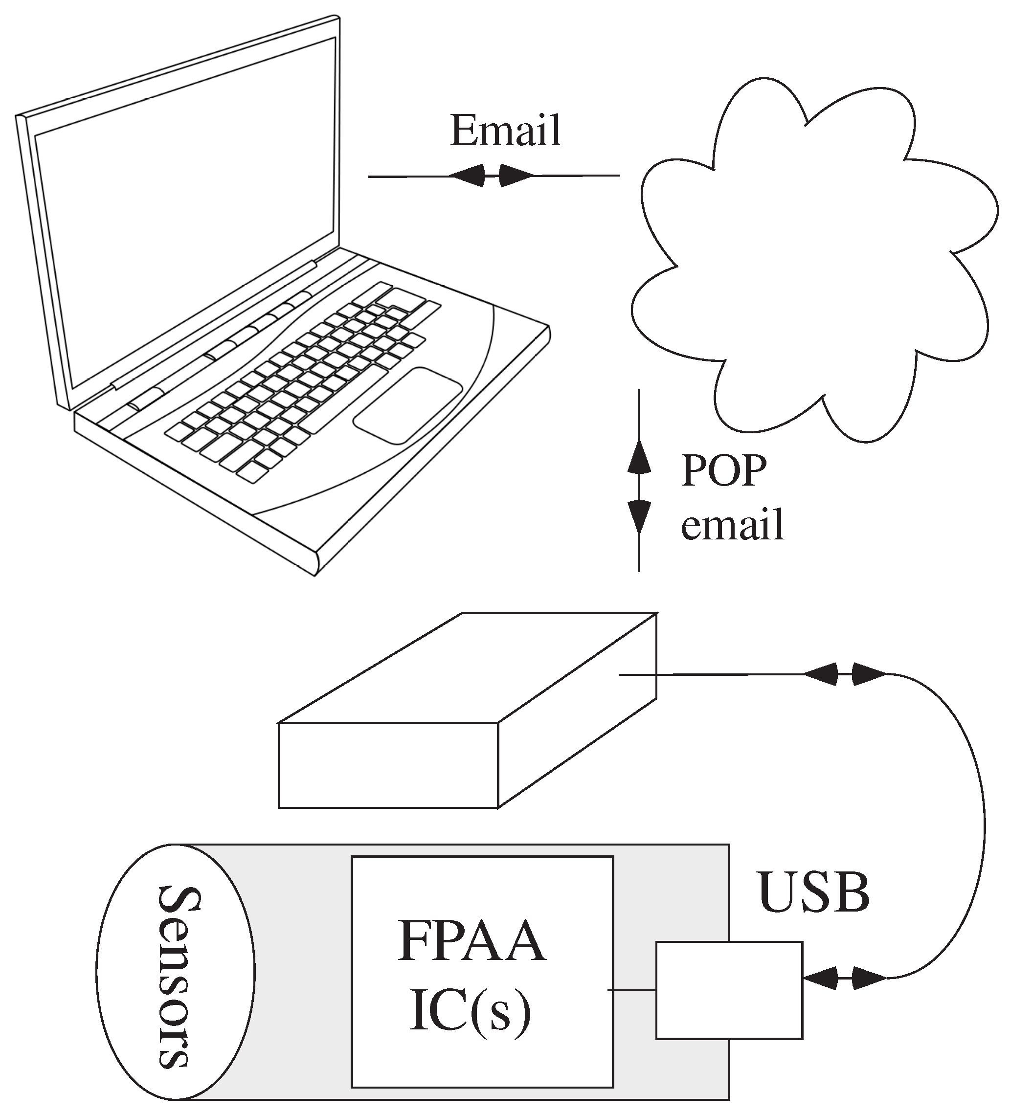
Figure 1 illustrates the remote test system requiring no additional setup, other than the experimental system, and simple email handling, available over almost all network systems. Independent of distance, the system enables users anywhere with an internet connection that is sufficient to send and receive email, providing opportunities both in academic as well as research and industrial applications. This approach minimizes computer support setup and maintenance, relieving the pressure on overworked computer support staff, particularly in cost-conscious academic environments, as they try to keep pace to maintain a larger number of computing systems. Those creating the system do not require any web hosting, as well as any web-based executable functions requiring numerous signoffs and security checks for any code iteration. The system only requires a simple unmanaged WiFi or cable connection, even including university guest WiFi or WiFi in a coffee shop. Computer administrative staff will have no further knowledge of this system compared to a guest user on an unsecured WiFi. One can imagine extending this concept to a number of remote sensor nodes.
The remote test infrastructure is enabled through a single external digital interface to an analog–digital programmable and configurable IC system, empowered using large-scale Field Programmable Analog Array (FPAA) device(s) [
7]. This approach gives a simple digital peripheral using a standard interface (i.e., USB), enabling a small Internet of Things (IoT) block interfaced through an email system to an open-source design/control tool. Our open-source tool platform empowers the user to do seamless low-power analog-digital co-design in a single environment [
8]. The resulting controlling device, whether it be directly connected through this digital port (i.e., phone or tablet) or through a network, can be a potentially simple OS enabling all features on the resulting system, including sensory/actuation devices connected to this remote platform.
POP (Post Office Protocall) email communication requires only a few limited operations, requires simple coding, and requires minimal web-based computation requirements for operation, particularly for academic environments. Email protocol simplifies individual access while requiring effectively zero administrative support. Other educational remote test systems require the user to take control of the system, usually through a log-in. This remote system approach differs from the area of one-way updating FPGA software, or remote FPGA reconfiguration for a device in the field [
9,
10].
The following sections present the resulting FPAA based remote test setup including overviewing the remote-tool structure, overviewing the FPAA devices and Baseline Tool Framework (BTF) for a self-contained discussion, presenting multiple system examples, while presenting the range of user interfacing, and expanding the remote user application as well as measurement capability.
1. Remote Tool Framework and FPAA Overview
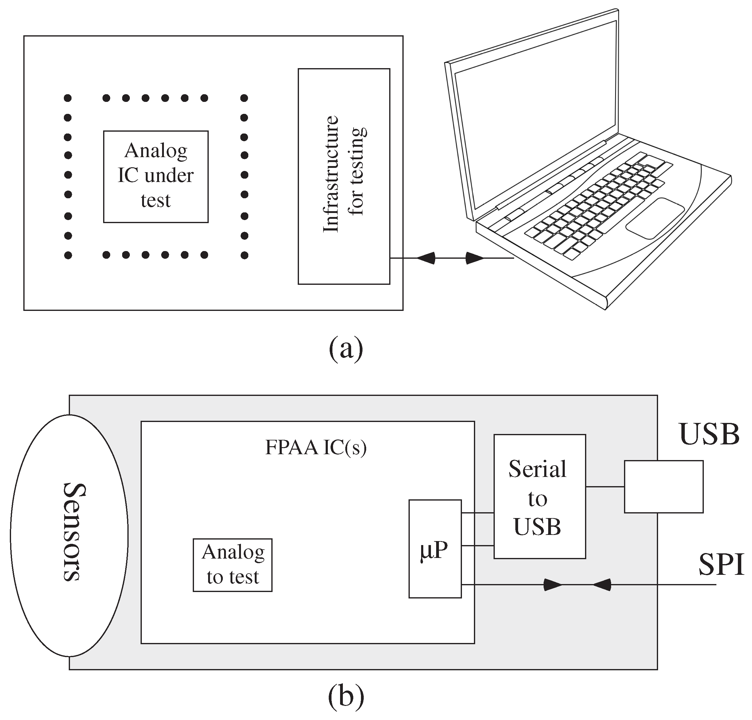
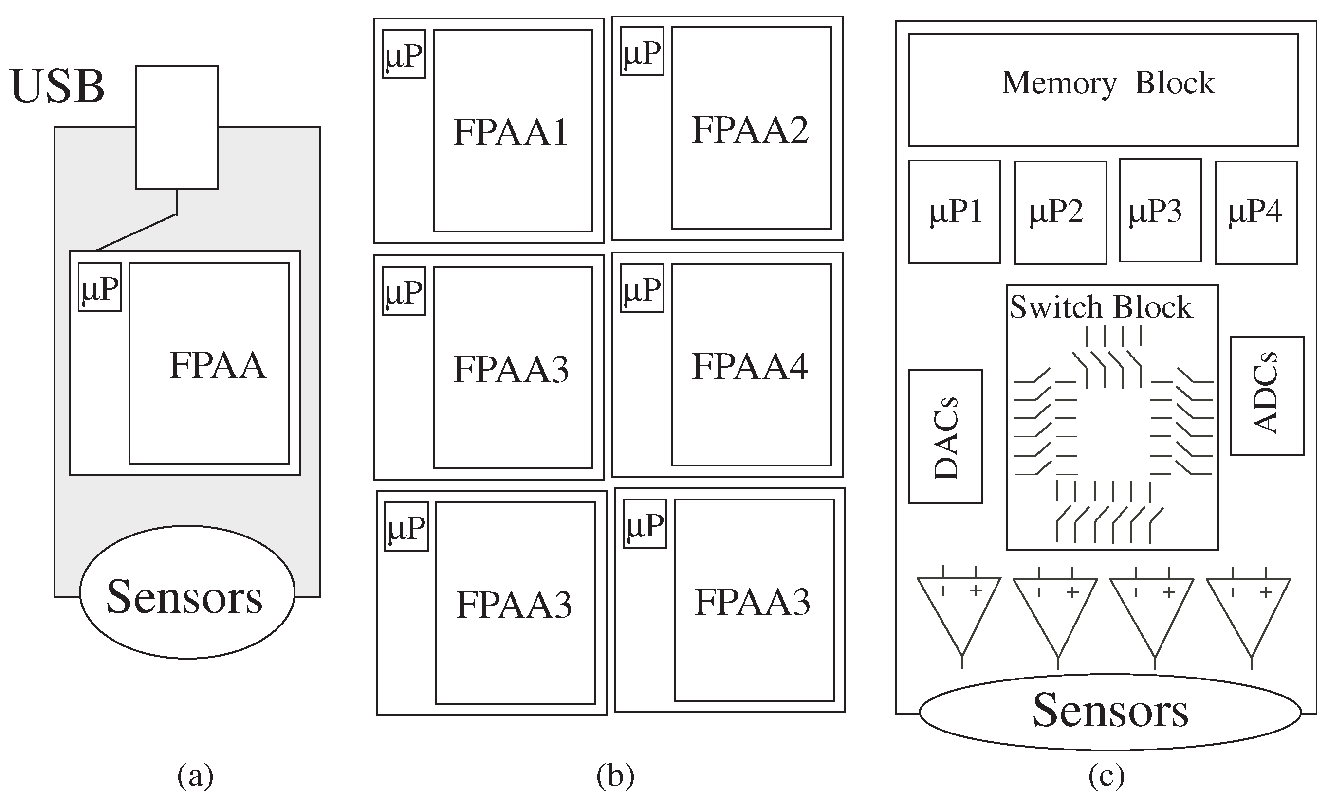
Figure 2 shows the perspective of our remote testing approach. When one thinks of testing an analog IC, or even a mixed mode IC, one tends to visualize, in the best case, a test setup like
Figure 3a. Such systems mostly have a single or a group of analog ICs, some controlled switches, and an infrastructure to connect to a computer to control the entire setup as well as run the testing interface. When looking at a remote testing system, the testing interface layer requires further complication depending on the particular system.
In comparison,
Figure 3b shows the FPAA system used in this paper. The FPAA IC is a full system with a processor, requiring only simple interfacing to the outside world through USB or say SPI ports, appearing to be a standard peripheral to a typical device. Such an approach enables a family of configurable hardware, utilizing a single configurable framework and tool infrastructure to control the resulting device. This difference in configuration provides the opportunity for empowering our remote test system for classroom use, research groups, as well as interested users. Integrating this approach into an existing tool framework keeps compatibility for a range of applications, and not limited to just an academic or research application.
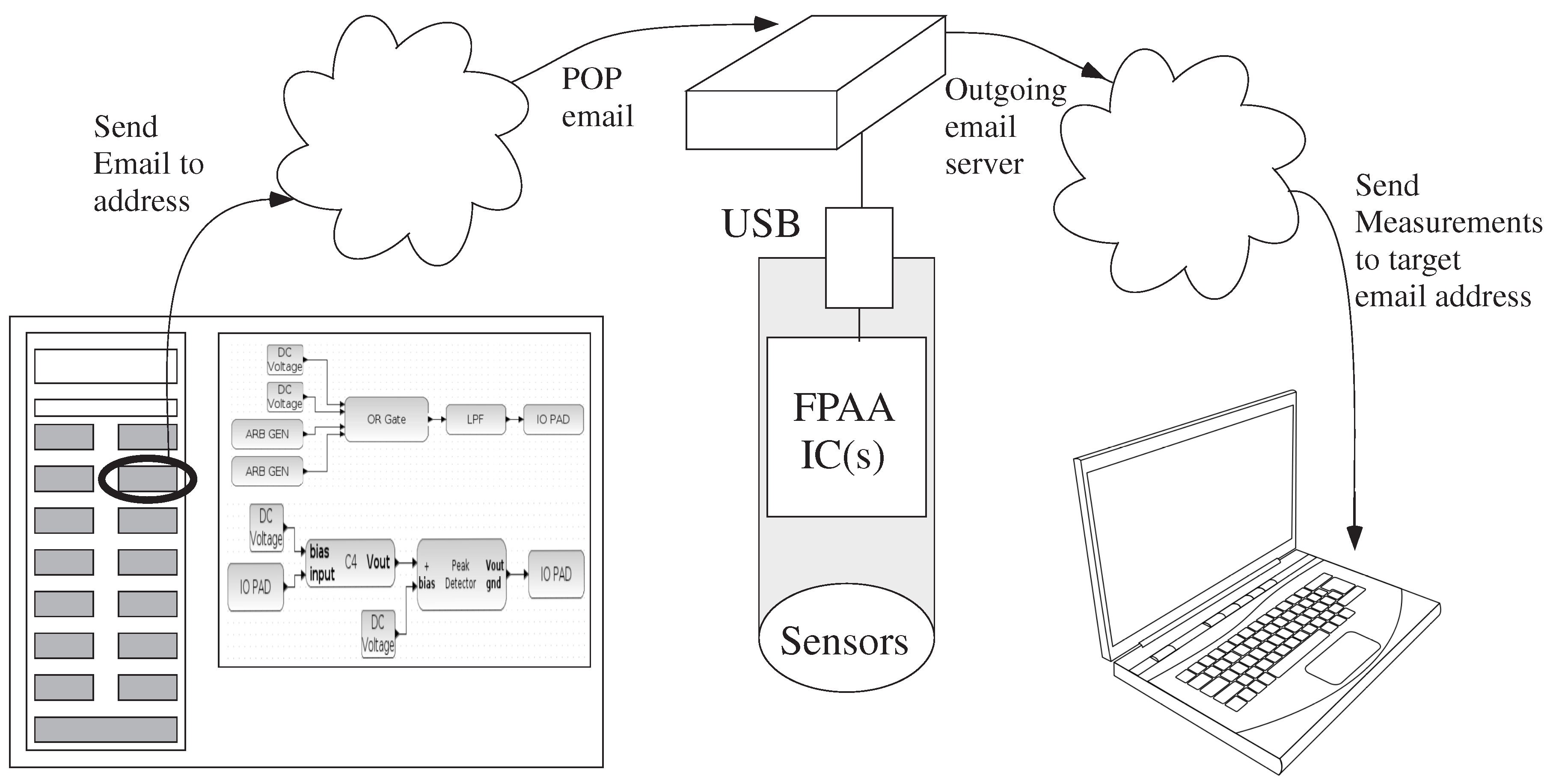
Figure 2 shows the framework for the remote system approach. The resulting structure should be easy to use on both the user and remote server side, requiring minimal user maintenance, using an integrated user tool platform, and having as few location constraints as possible. The tool platform [
8], implemented in Xcos/Scilab (an open source clone for MATLAB/Simulink), simulates designs as well as enables experimental measurements after compiling to the same integrated design tool framework. The open-source toolset is setup as an Ubuntu 12.04 Virtual Machine (VM) (available at
http://users.ece.gatech.edu/phasler/FPAAtool/index.html) enabling use in classrooms as well as research and development groups.
Our modifications to the high level Xcos tools on the user side required extending the GUI interface, as well as updating the (Python) code to enable emailing the resulting compiled FPAA targeting file out from the VM. The user will receive their resulting data to their email location as an attached representation of the measured results; the user can move this data into Scilab or another analysis/plotting tool of their choice. By using an email based system, one would not expect real-time control occurring through the resulting email network.
The small remote server code framework minimizes resulting system overhead, utilizing standard email servers to enable a capable, relatively stable remote platform with nearly zero administrative overhead. The remote server will periodically check for email on the server, POP the resulting message from the server, check its control syntax, and have the object code ready for programming. Recent FPAA devices now enable Floating-Gate (FG) device programming entirely on the device as an input data stream; therefore, the entire data stream, including μP code to execute programming, simply looks like a single stream of data to the system. Encapsulating this entire structure in a single file requires small, Unix-based code to communicate the file to be programmed. After the device is programmed and the input data is loaded into the processor, the IC proceeds to compute the resulting function, also storing data in local or in the remote server memory. The resulting output data results are pulled together and sent out by email to the host’s chosen email address.
This approach enables programming by any small embedded devices (after design), particularly those with direct USB connections (tablet, phone) allowing minimal (Linux) code for programming and operation. Whether remote or not, these concepts allow an easy approach for networks of remote sensor nodes; for example, an IoT approach enabling real-time sensor processing that can send context aware results while requiring minimal support overhead for the approach.
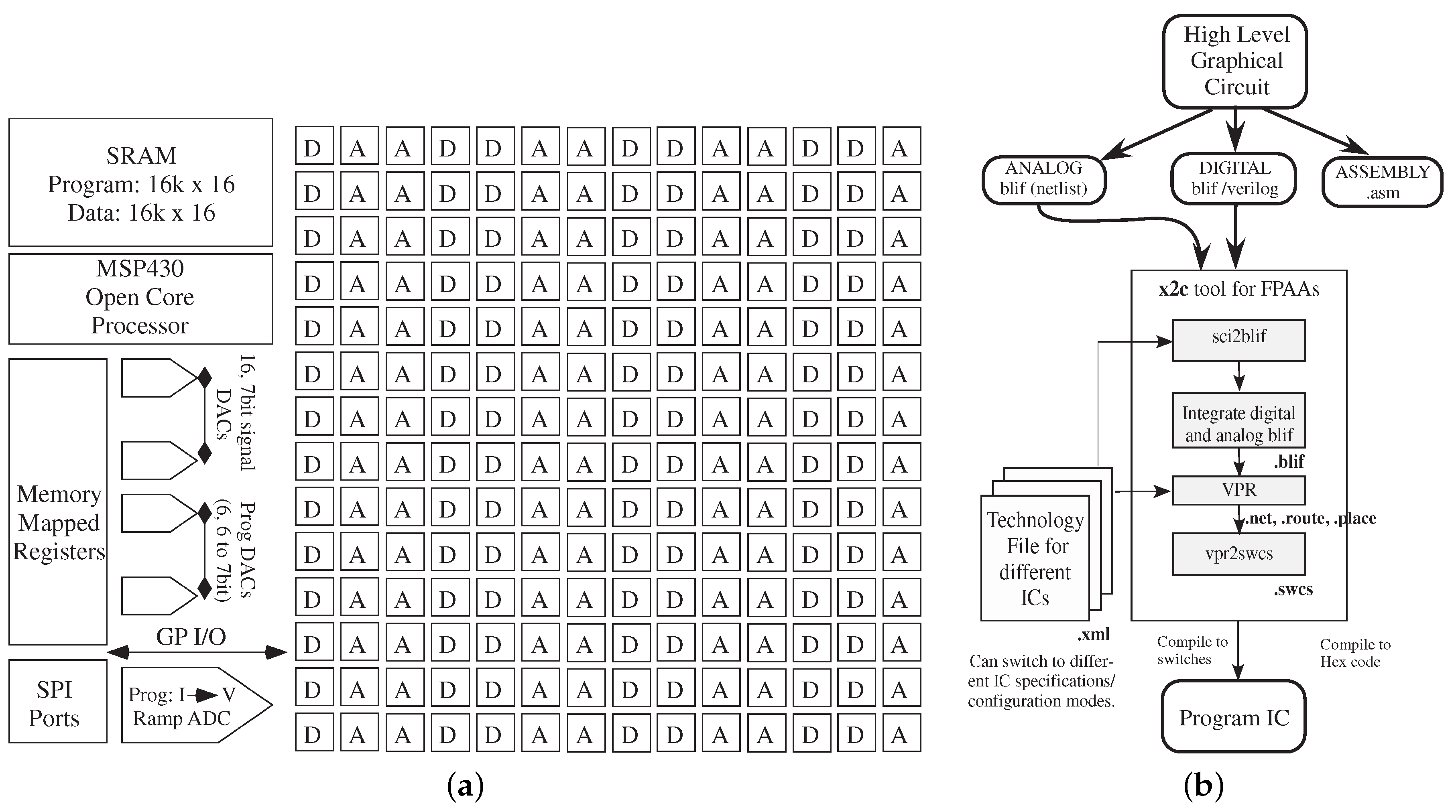
Figure 4a shows the block diagram of the SoC FPAA used in this paper for experimental measurements [
7]. This SoC FPAA enables nonvolatile digital and analog programmability through Floating-Gate (FG) devices, both in the routing fabric, but also for parameters for the computing elements.
Figure 4a shows a typical FPAA block diagram that enables both analog and digital components in its Manhattan routing fabric, and most approaches for FPAA devices can be fitted into this resulting framework [
11,
12,
13,
14,
15,
16]. The blocks with simple digital components are called Computational Logic Blocks (CLB), and the blocks with analog and digital components are called Computational Analog Blocks (CAB). These devices enable useful computation out of using routing resources, such as Vector–Matrix Multiplcation (VMM) built out of the routing crossbar (i.e., floating-gate) switch matrices. These approaches are shown to generalize to building signal processing and classifier blocks [
7].
Figure 4b illustrates the tool flow using a mixed-signal library of components. Large FPAA devices [
7] require user friendly design tools to enable system design without requiring understanding of analog circuit components. This framework integrates a high-level design environment built in Scilab/Xcos with a compilation tool,
x2c, to compile from high level description to a targetable switch list to be programmed on the FPAA device.
x2c is composed of
sci2blif, and translates a block in scilab to .blif format, our modified VPR (Versatile Place and Route) tool [
17], which acts as an input to
, as well as modified architecture files for analog–digital SoC. The graphical high level tool uses a palette for available blocks that compiles down to a combination of digital and analog hardware blocks, as well as software blocks on the resulting processor. Simply pressing one button in Ubuntu brings up the entire graphical working toolset. The approach allows a given user to access and use this toolset on their remote computing devices with minimal effort. This tool could be modified for other configurable structures, so the approach is wider than just FPAA devices.
Figure 5 shows FPAA IC board design, as well as systems using additional programmable components. The high-level graphical tool enables a user to be able to try different approaches to optimize the system performance, allowing consideration of tradeoffs of power, system utilization, time to market, etc. Digital Hardware–Software CoDesign is an established, although unsolved, discipline, starting from its early work [
18]. Although engineers do design mixed mode systems, one still has many open questions of methodology in this field [
19,
20,
21]. Including programmable and configurable analog computation to current digital approaches requires revisiting existing tradeoffs. The approach is focused on enabling system designers to integrate useful systems, while still enabling circuit experts to continue to develop creative and reusable designs within the same tool flow.
2. First Remote System Overview Example: Low Pass Filter
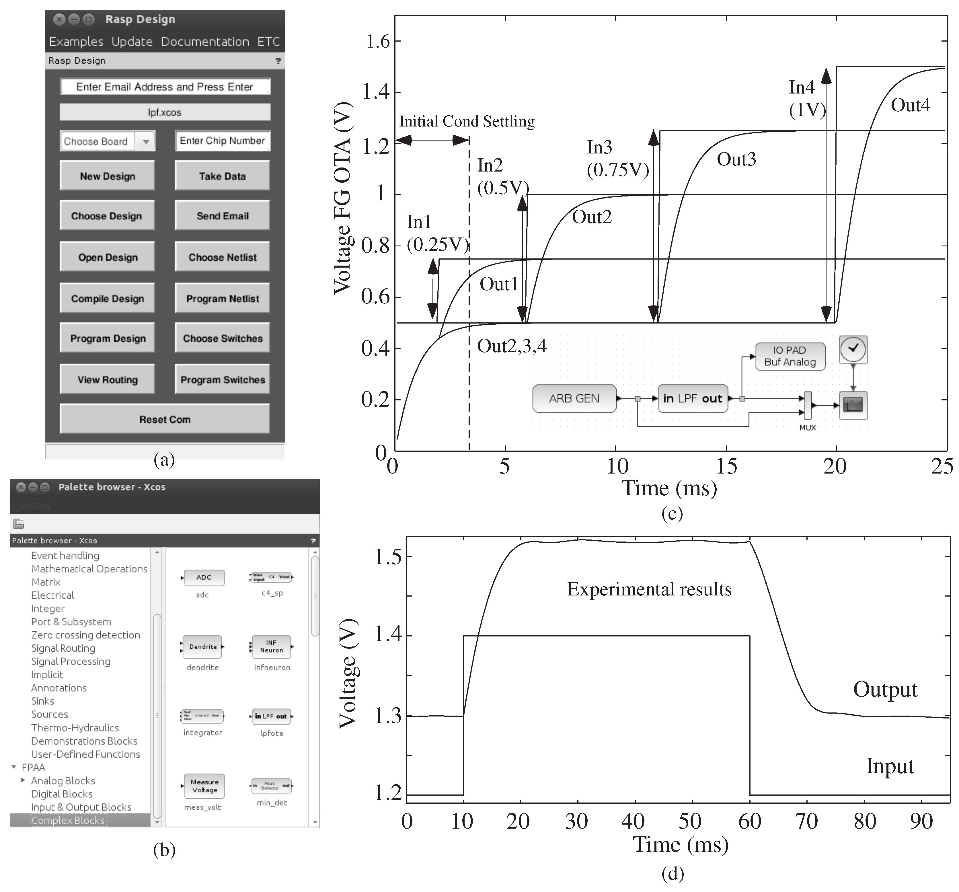
Figure 6 shows an initial full tool example of the graphical interface and results for a first-order Low-Pass Filter (LPF) system, showing both simulation results and experimental results from the remote test system.
Figure 7 and
Figure 10,
Figure 11 and
Figure 12 show more complex tool examples using this remote system; we use this example to discuss the remote tool flow in detail. Xcos gives the user the ability to create, model, and simulate analog and digital designs [
8]. The Xcos editor is standard blocks that are compartmentalized into classes or palettes that range from mathematical operations to digital signal processing. The editor allows the internal simulator to utilize the functionality of each block to compute the final answer. Our tool structure took advantage of user-defined blocks and palettes that can interact with Scilab inherent blocks.
Figure 6a shows the FPAA Tool GUI and grey buttons with the labels: New Design, Choose Design, Open Design, Compile Design, Program Design, and Take Data; these buttons open a new Xcos editor window, select a previously saved design, view the design in Xcos editor, convert the information in Xcos file into a programmable format, program hardware for the current Xcos file selected, and cause the hardware to be in the mode to take data, respectively. It includes a button which is labeled
email, and a top box that one can put in an email address. These two small buttons on the tool framework show the minimal additional user overhead for using the remote system.
Our Xcos [
22] tool uses user-defined blocks and libraries. When the user opens the Xcos editor, a palette browser is displayed, as shown in
Figure 6b. The browser lists Scilab’s collection of palettes as well as user defined palettes. One selects from a palette of available blocks to build the resulting system, which can be composed of a mixture of analog (blif), digital (verilog, blif), and software (assembly language) components. The Palette for FPAA Tools contains sub-palettes for blocks that are classified as analog, digital, inputs/outputs, and complex blocks. The Input/Output palette contains typical circuits like DACs, Arbitrary Waveform Generator, I/O pads, and Voltage Measurement. The digital palette contains typical circuits like a D Flip Flop and a clock divider. A few examples of complex blocks are an Low-Pass Filter (LPF), a Sigma-Delta ADC, and a VMM + Winner-Take-All (WTA) Classifier.
The single programming file, attached to the email for programming the remote system, is a compressed structure of multiple files. The tools output a single programming file, a combination of multiple files, that is used for FG programming and SRAM memory setup for the SoC FPAA [
23]. The design tools can process the downloading of this file, as well as other devices (e.g., remote computer, tablet). The SoC FPAA devices now enable Floating-Gate (FG) device programming entirely on the device as an input data stream, therefore the entire data stream, including
μP code to execute programming, simply looks like a single stream of data to the system. The FPAA utilizes an open-source
μP, embedded 16k × 16 SRAM for program and data memory, as well as the memory mapped registers for FG programming. We give the file definition in
Table 1. The current system loads all of the data into the data SRAM ( 16k × 8) for this remote system. Currently, larger waveforms would require reloading the data SRAM and continued processing. We could compile an SPI port on the digital infrastructure and interface to the USB communication enabling streaming of larger data through USB. We expect this structure will remain stable across future generations; fortunately, each programming file is self contained for programming since it includes its own code and parameters for programming.
We explicitly kept the requirements for the computer as minimal as possible. We implemented this system running on 8 year old laptops running Ubuntu 12.04. These systems are considered too old for our computer support staff to allow on our network, and would be prohibited on the internal network. The basic requirements for this system as we have currently implemented the system include a flavor of Linux, a system capable of executing Python (3.4) script, that includes implementing an email POP server, a USB port to communicate with the FPAA board, and WiFi access to an open network. We also require email accounts for the communication between these blocks.
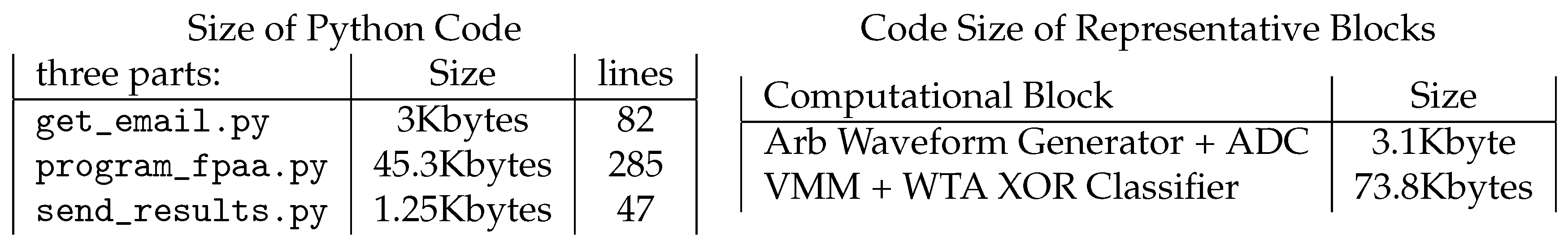
Figure 8 shows the size of the three Python code modules required for this remote system. We expect these systems can be further reduced in complexity, both in code (Python) size and complexity. For example, one could easily imagine a device like a Raspberry Pi (e.g., Pi 3 versions with WiFi) [
24], a device explicitly forbidden on our internal teaching and research networks. A Raspberry Zero with a wireless module attached could easily perform these operations.
3. Additional Configurable Remote Platform Considerations
This approach gives a simple digital peripheral using a standard interface (i.e., USB), enabling a small IoT block interfaced through an email system to an open-source design/control tool. The resulting controlling device, whether it be directly connected through this digital port (i.e., phone or tablet) or through a network, can be a potentially simple OS enabling all features on the resulting system, including sensory/actuation devices connected to this remote platform.
Although the use case presented seems fairly simple, we believe this system is in the family of IoT devices,
“IoT is the network of physical objects that contain embedded technology to communicate and sense or interact with their internal states or the external environment.”
This remote system fits this definition, particularly as it expands to larger number of systems and users.
“The IoT is significant because an object that can represent itself digitally becomes something greater than the object by itself.”
Building a configurable mixed-mode system to have a standard USB and network interface enables these devices into the IoT space. Most IoT systems are not so small, or power constrained, but this system, coupled with sensors, integrates with this device and directly fits the IoT concept.
The authors chose a POP email system among the many alternatives for system communication. First, the simple structure of a POP email system (see for example [
28]) fits with the limited operations required, is easy to code, and keeps the resulting computation requirements for operation as minimal as possible. POP supports simple download-and-delete, where this system only requires connection, message retrieval, and temporary storage (local). Anything more complex is extra overhead with little function. Email is ubiquitous, particularly for students. The wide variety of email services (e.g., Gmail) results in many painless options, without the need for server infrastructure. A simple POP server keeps the control code small allowing systems extending to small, remote platforms (e.g., devices worn on the body, etc.), particularly where low power battery operation is possible.
Second, starting from the inspiration of academic classroom experiences, the use of email protocol simplifies individual access while requiring effectively zero administrative support. For example, this remote system is being used in a graduate course this Spring 2016 [
29]. This remote system approach allows a host system to even be operated anywhere, such as a coffee shop, without significantly affecting the system users. Most can get some form of a wireless network allowing basic email protocols on that network. Any administrative barrier for faculty to set up technology for their classes tends to result in the approach not ever being implemented. This remote system provides an alternate path through the constraints of the layers of resources and administration of those resources. We expect such a system can have significant research impact, and the ease of collaborators having shared systems opens up options for remote sensing and computing nodes with nearly zero required resource support.
Other remote test systems used in education typically require the user to remotely log-in to the system, and effectively take control of the system. From one of the classic circuit measurement systems [
30], one sees attempts for remote test structure to replace a large number of dedicated lab stations with expensive equipment, similar to the setups used at Caltech CNS 182 (CNS 182: Analog VLSI and Neural Systems course taught at Caltech between 1983 and 1996, using the textbook by the same name [
31]. The course no longer exists, and nothing is hosted on Caltech sites any longer.), and later at Georgia Tech (GT) utilizing similar dedicated lab stations that transformed into the earliest FPAA devices [
29]. Additional remote systems have attempted other concepts having users log-in and control a remote computer [
32,
33,
34,
35], as well as debates over the right use of remote hardware for classes [
32]. These approaches involve using a hardware board (e.g., Spartan 3 or Arduino board) and using graphical languages like Labview (e.g., [
36]). Much of the time on the system relates to the user thinking about their problem, rather than performing operations on their experiment; this paper’s system gets around these issues while using a tool approach identical when a physical board is used.
This remote system approach is different from the area of one-way updating FPGA software for a device in the field. Remote FPGA reconfiguration already utilizes internet connections on allowed networks (with any resulting permission overhead), and can update FPGAs using protocol like User Datagram Protocol (UDP) [
37]. Xlinix provides direct developer support when using external devices (e.g., CPLD) [
9], or even cases using the FPGA as part of the updating infrastructure [
10]. Hardware systems are designed for in-field FPGA updating [
38], including space applications [
39]. This paper’s remote system looks towards an expanded purpose, while also not being subjected to any network infrastructure constraints. This system may in fact be used by the authors for updating of FPAA and other configurable devices in the future, although this application is not our driving motivation.
Security management was not implemented in this first system implementation, but is a focus area going forward. One would want a form of authorization (i.e., a user access code) as part of the email message. Using a reduced email based system does reduce a significant amount of potential security issues compared to a web-based system, as well as not needing to support a wide range of internet browsers. The Linux based system and email retrieval system is used to download files, extract resulting targeting files, and use those files for targeting; we do not use an entire email browser for the resulting system, eliminating many potential virus issues. The biggest security issue seems to be uncompressing the resulting files, where that is the only place we need to execute anything on the files, and should be developed as a trusted source. We also expect a host of issues will arise as people work with such a system where outside groups, say running the remote system, might have exposure to the user’s designs, and resulting Intellectual Property. We expect current approaches towards individual security will be used where applicable.
4. The Range of User Interfacing Expands Remote User Capability
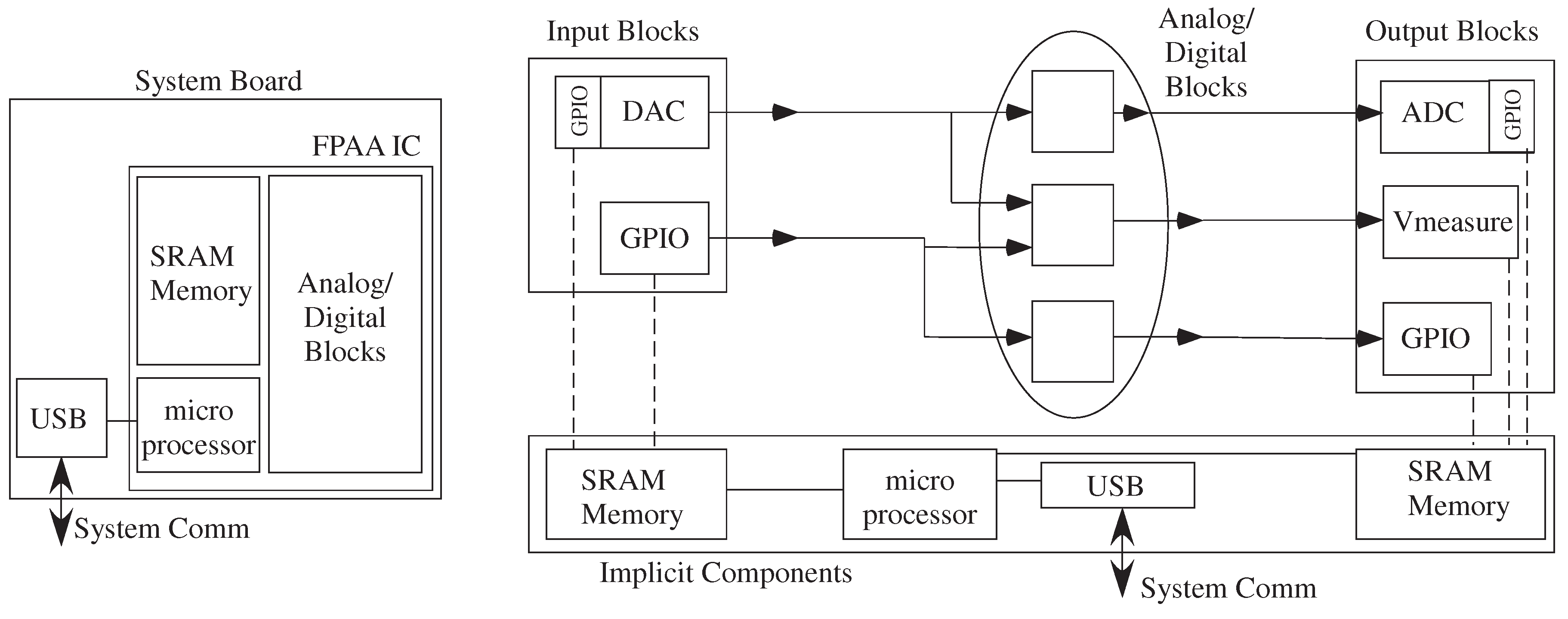
Figure 9 shows that the remote server was partially enabled by a simple digital (USB) interface, with simple interfacing between the FPAA IC (or multiple ICs) to the resulting USB infrastructure to the host device. The input data, output data, FG programming, and other control functions all move through a single standard digital USB interface; the device to the remote system looks like any other embedded, USB peripheral, where the tools handle a similar case whether the board is local to the tools or emailed to the remote server. The user needs to understand both the analog and digital capability of the FPAA IC, and the resulting input and output blocks for the system as well as the resulting system control, at the level allowed for the high-level tool framework (Xcos/Scilab). A user will often use digital (GPIO) or analog (DAC through GPIO) input blocks, interfaced through the SRAM memory and
μP control, and will often use digital as well as analog compiled ADC through GPIO or Vmeasure through slower and more accurate 14-bit ADC. The tool framework compiles down the resulting analog, digital, and
μP components, as well as the vector input into the system. The setup uses no external pins; one could connect multiple devices, heterogeneous devices, and additional sensors, but to the external world, the device is still a simple USB connected device. The USB interface is connected through serial interfaces, using a simple serial (8n1) interface through an FTDI 2232D IC (FTDI, Glasgow, Scotland) on the board.
Figure 9 shows the high-level blocks representation, similar to the corresponding Xcos diagram, both including computational blocks, as well as input and output blocks available and their interfacing into the
μP/SRAM memory block. The arbitrary waveform generator connects data to a vector input representation versus time in the Scilab workspace that gets converted, where needed (i.e., DAC devices), as well as packed with the programming file; the interface for the data is directly set by the high-level tools. A short list of potential on-chip interfacing options for moving data in and out of the
μP/SRAM memory are:
General Purpose Input/Output (GPIO) memory mapped digital registers;
Hardware interrupts based on routed fabric signals;
Signal DAC through memory mapped registers;
Compiled ADC coupled with FG elements in the fabric through GPIO registers.
These approaches are all voltage-mode inputs and outputs, consistent with level = 1 block definition for system building [
40]. Furthermore, blocks can have some assembly code (or completely assembly code) as part of the functionality, and, therefore, would interact with memory, potentially, more directly. Where necessary, one can measure currents through compiled transimpedance amplifiers, switched capacitor networks, and related circuit techniques. One key constraint on any algorithm is efficiently using the 16k × 8 SRAM data space either to hold data, or buffer data coming through the serial communication from the host system running the remote interface.
The availability of ADC blocks determines the particular computing architecture.
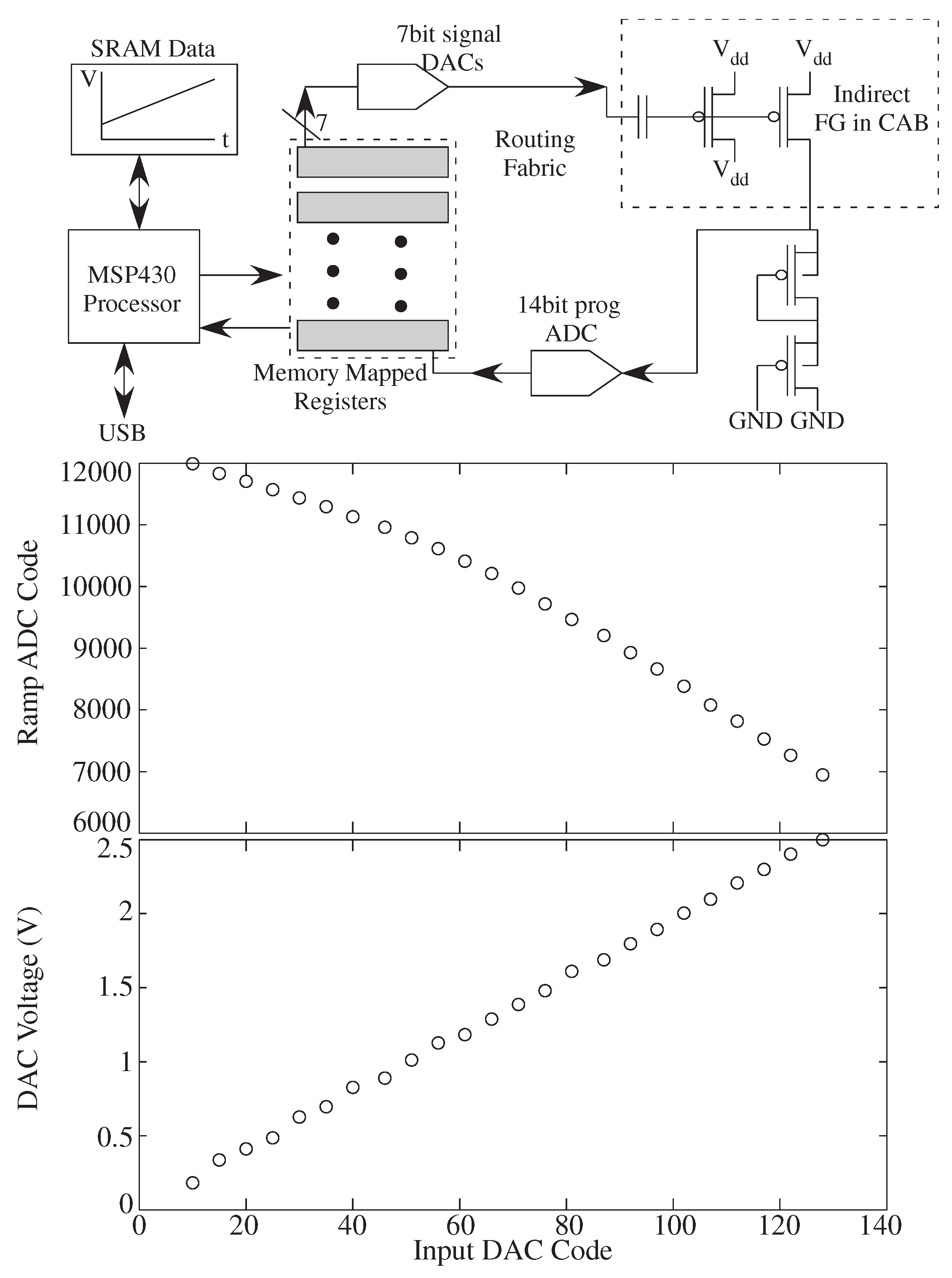
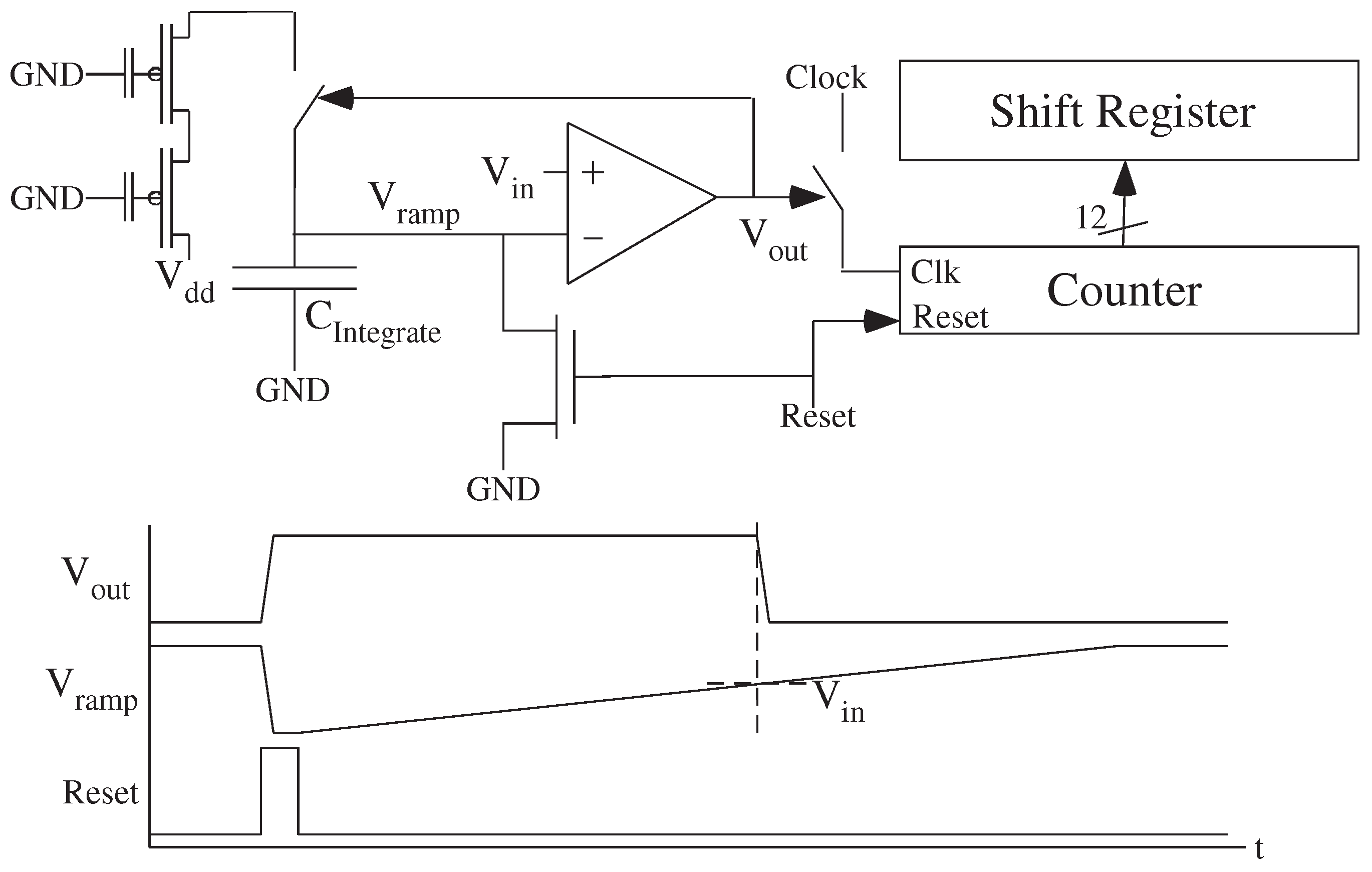
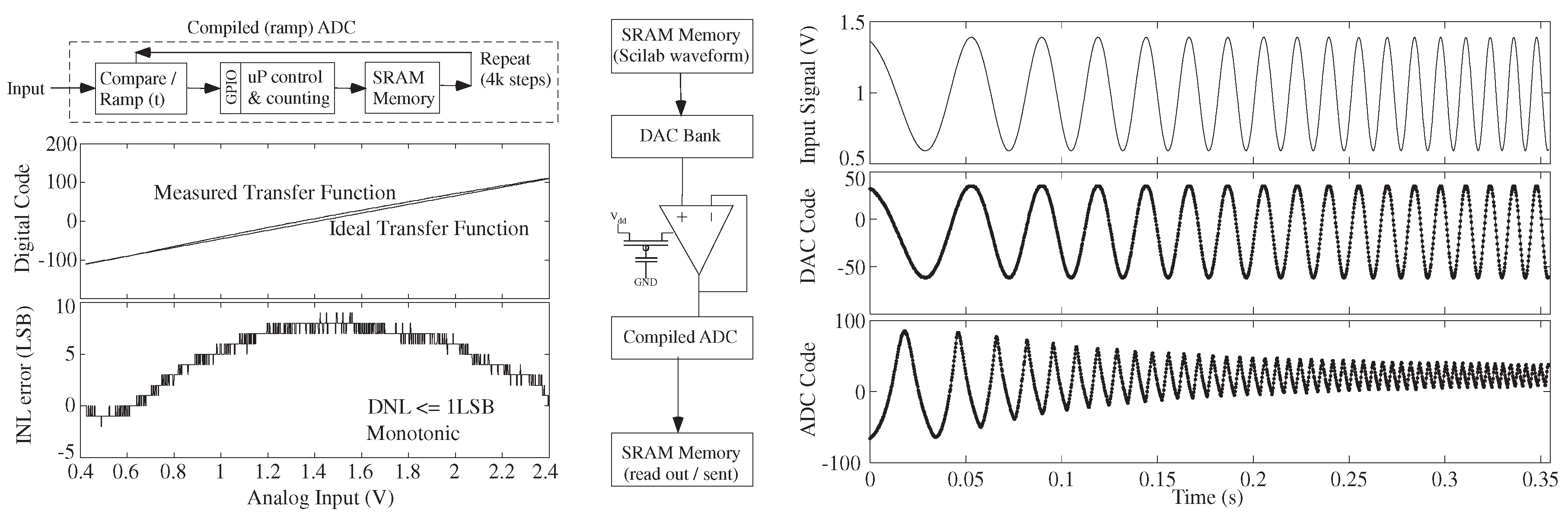
Figure 10 shows a compiled ramp ADC in the FPAA fabric; one would want a wide library of FPAA compilable ADCs using the FG device density. A pipelined one-bit ADC architecture would be the lowest practical latency because computation requiring smaller latencies would be done in analog. These devices are used mostly for acquisition of data or circuit debugging. Algorithmic converters, being related to the pipelined ADCs, would most likely win over successive-approximation ADCs because they do not require designing a separate DAC for the system.
Figure 11 shows a simple compiled ramp ADC converter to illustrate the flow from input SRAM memory data to the computed output SRAM memory data. The resulting simple 8-bit ramp ADC illustrates using the digital infrastructure and
μP to move analog signals into stored SRAM memory. The simplicity only requires part of a single CAB element while still giving reasonable monotonic performance with some curvature due to the nonideality of the current source element creating the ramp; Measurement examples use 4k Samples per Second (SPS) ADC sampling.
Figure 11 shows a complete computing loop for data through a board used as a remote test. The initial data is loaded into SRAM as part of the programming structure, processed through one of multiple memory mapped seven-bit DACs, processed through a first-order LPF block programmed with a corner frequency of 150 Hz, and measured through the above ADC block, arriving back as stored solution vectors in SRAM that are transmitted back to the user. The LPF block is the programmable Transconductance Amplifier (TA) with the resulting routing capacitance, as used in the previous section; G
-C filter topologies utilize line capacitance setting the filter corner by the transconductance of the OTA amplifier. This compiled ADC integrates the compare + ramp functions compile into a single CAB, routing the digital output bit to GPIO. The ADC polls for the digital bit to change while counting in the processor; more advanced blocks utilize interrupts and compiled counter blocks in the CLBs for the conversion. The ADC is not meant to be the highest precision component, but a very small, monotonic ADC calibrated for the resulting response as necessary.
At this stage, one might ask how the system handles users or student bugs in their compiled code. The system allows for bugs, as well as debugging of the system. At one level, the system operates as programmed, particularly all of the hardware components. The input data will be applied, and the output data will be read and emailed to the user. Like debugging other software systems, the output results will potentially show the result of these bugs. The student/user will interpret the results, similar to other software systems, and modify their design accordingly. Furthermore, one could imagine bugs in the μP code that would hang the system. In this case, if the system takes too long to run (like 1 min), the controlling system halts the process, emails those results, and the system proceeds to the next item in the queue.
Figure 12 shows a more complex example using the remote FPAA system, a parallel bank of bandpass filters and amplitude detection typically used for low-power sub band analysis, as another example of co-design between assembly, analog, and digital components and interfacing. The corner frequencies are programmed between 100 Hz and 750 Hz, seen by the different peaks in the chirp response in
Figure 12. This example uses the same SRAM memory, seven-bit input DAC, and compiled ADC. A similar chirp signal linearly varies between 25 and 1 kHz.
5. Conclusions
We presented a novel remote test system, enabled by configurable analog–digital ICs to create a simple interface for a wide range of experiments. Our remote test system requires no additional setup, resulting both from using highly configurable FPAA devices, as well as from the advancement of straight-forward digital interfaces for the resulting experimental FPAA system. An analog–digital programmable and configurable IC system, enabled by FPAA device(s), requiring a single digital external digital interface opens opportunities for a simple remote test infrastructure. The system overhead requirements are straightforward, requiring simple email handling, available over almost all network systems with no additional requirements. We plan to release the open-source code for the remote system development after this journal paper is in press.
Opportunities appear both in academic, as well as research and industrial applications. This technical platform enables collaborators in different areas to investigate items on a single platform; setting up a system is straight-forward and capable for multiple systems. These approaches have been utilized as part of a graduate level class at GT [
29,
41]. Our novel open-source tool platform empowers the user to do seamless low-power analog-digital CoDesign in a single environment. Our FPAA SoCs consist of an integrated processor, I/O peripherals, and an FPAA comprised of analog and digital components [
7], although the approaches can be extended to other platforms. Our approach integrates multiple open-source tools, using Scilab and VPR, to develop a coherent user-friendly design flow, with a custom software toolkit that generates and implements high-level simulation and experimental measurement of the resulting hardware system [
8]. The ability to seamlessly move between tools designed for a board in hand as well as a remote test system has greatly improved the student’s interest in using either hardware platform, as well as keeping development complexity for such a complex laboratory course under control.


