
Sizing of SRAM Cell with Voltage Biasing Techniques for Reliability Enhancement of Memory and PUF Functions †


Abstract
:
1. Introduction
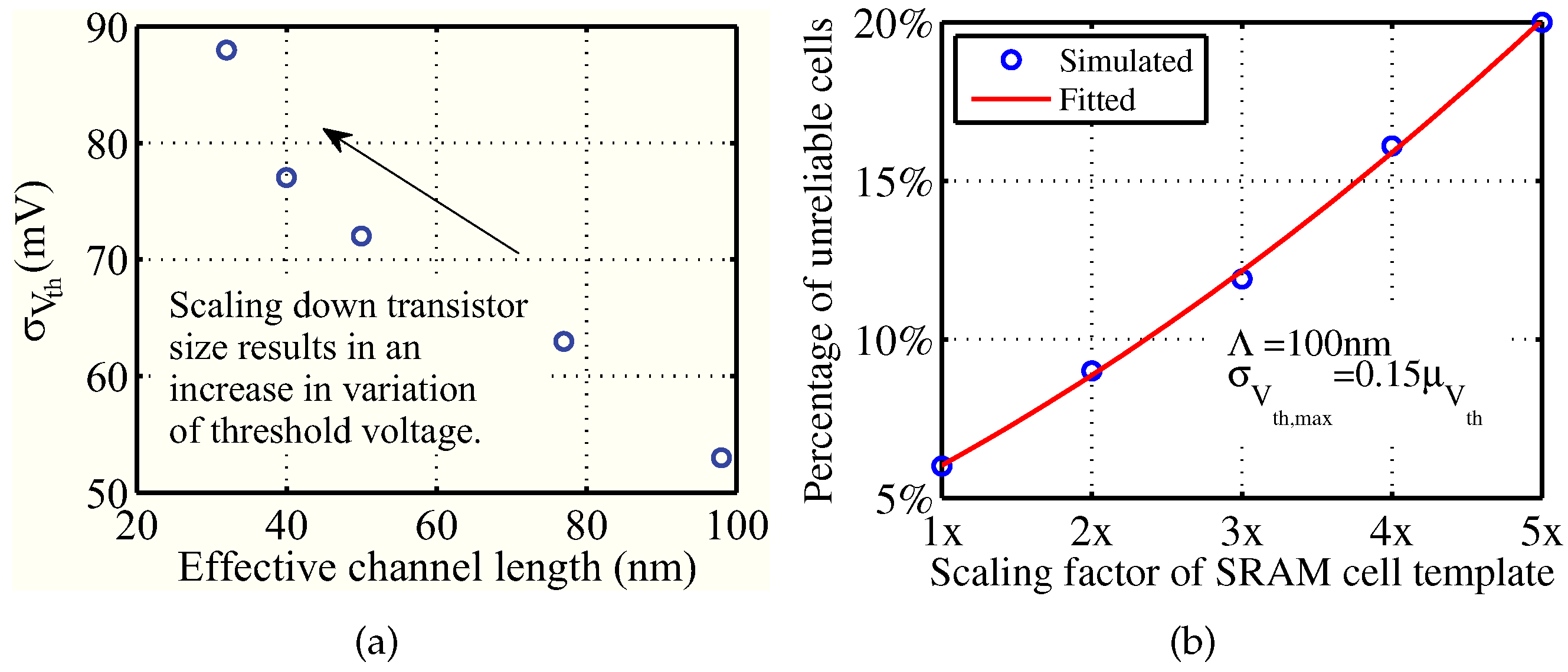
2. Impact of Process Variations (PV) on Different Operation Modes
2.1. Impact of PV on Physical Unclonable Function (PUF) Quality
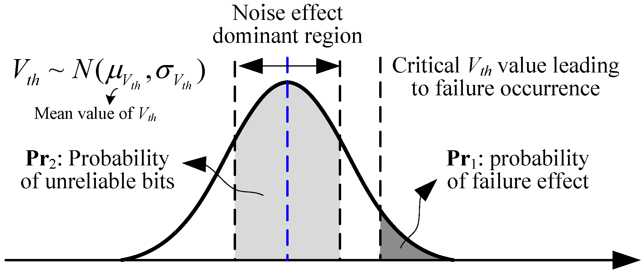
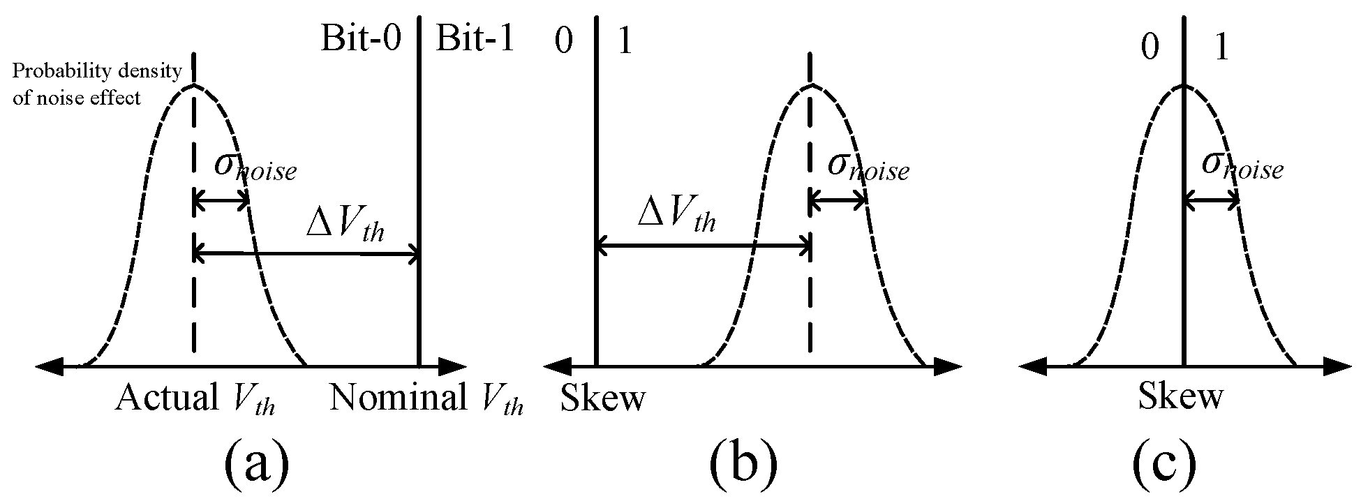
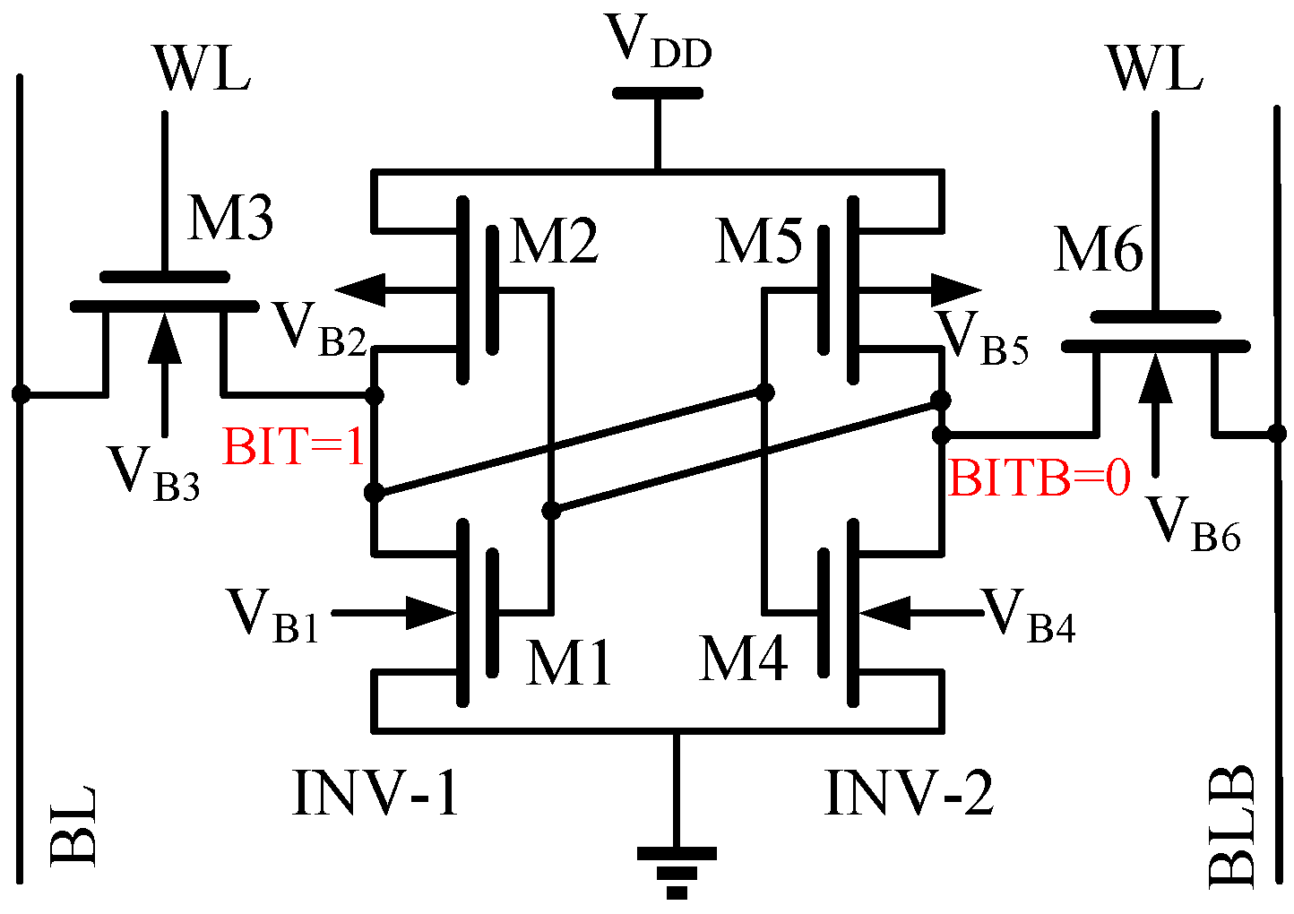
2.1.1. Mismatch of INV-1 and INV-2
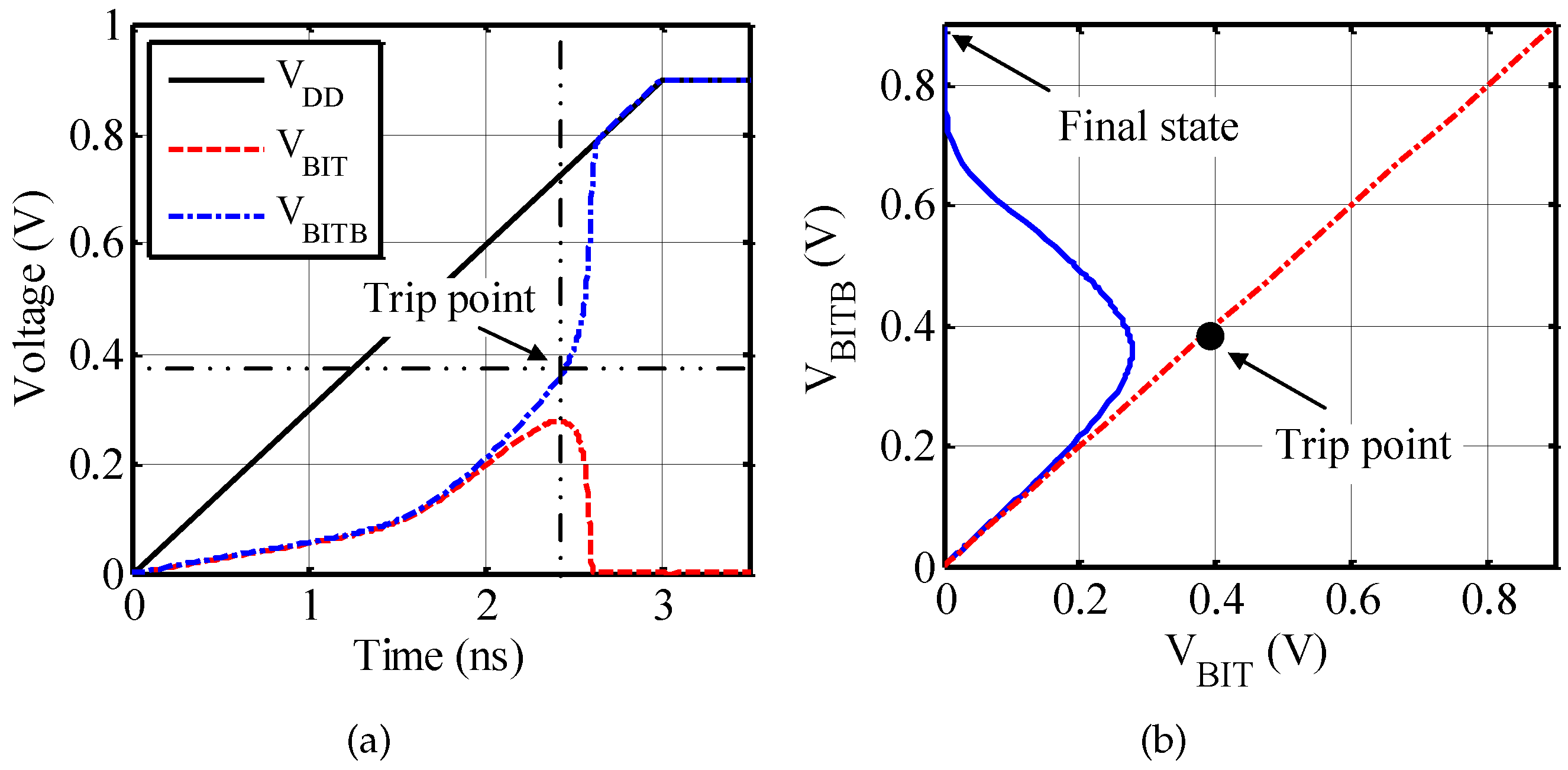
2.1.2. Loop-Gain at Trip Point
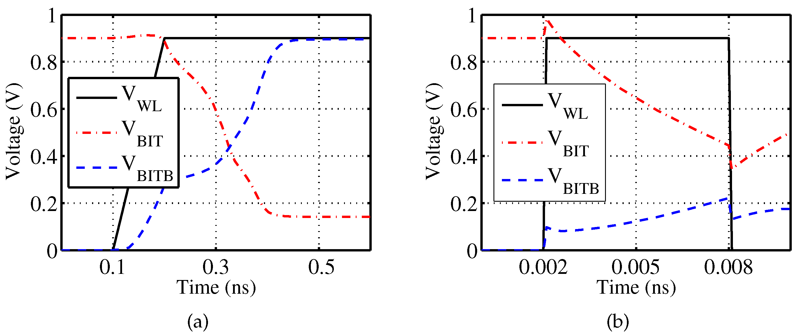
2.2. Impact of PV on SRAM Read/Write Failures
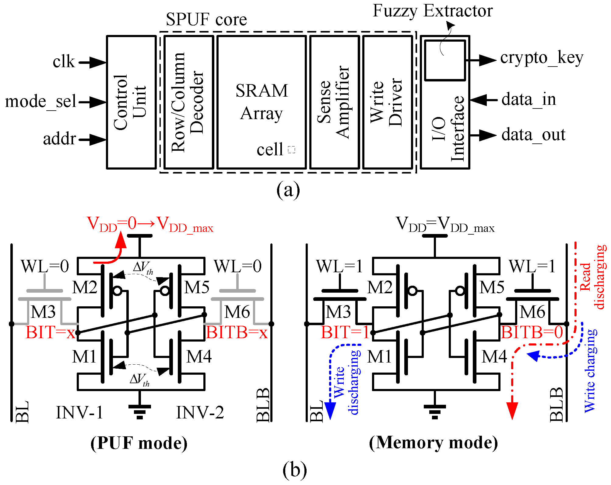
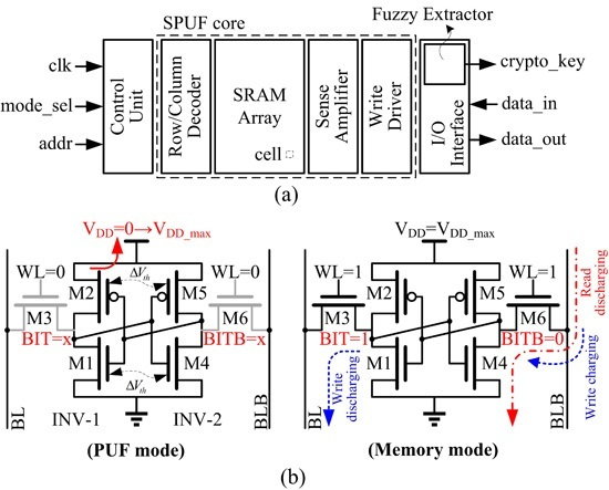
3. Proposed Design Method for Dual-Mode PUF
3.1. Circuit-Level Techniques
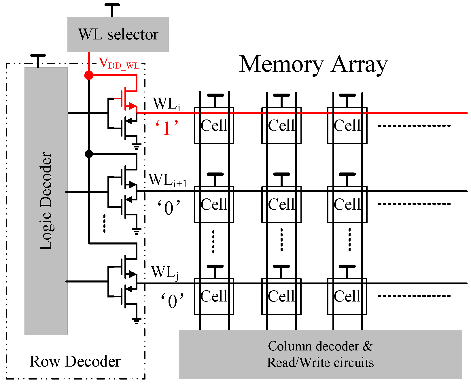
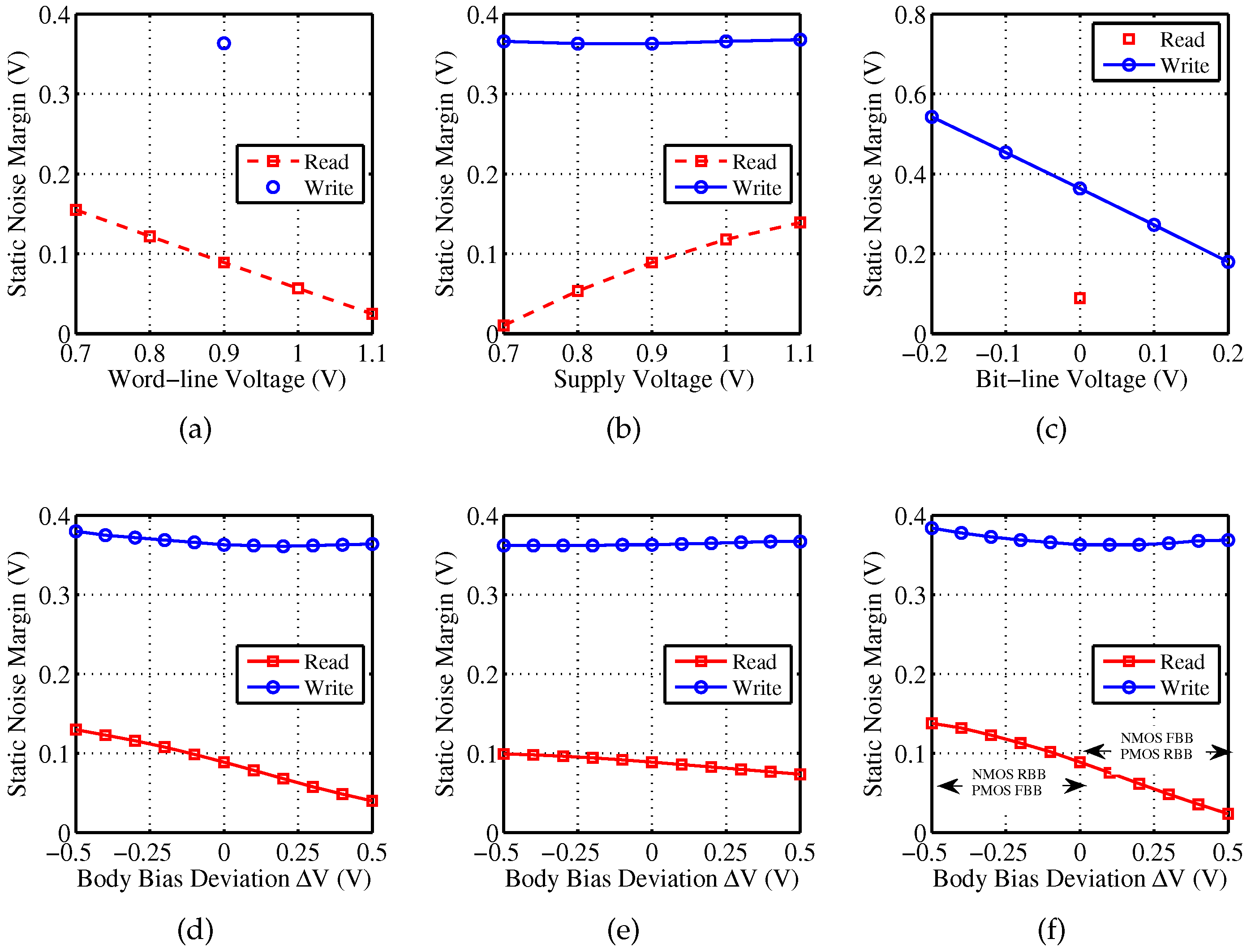
3.1.1. WLM
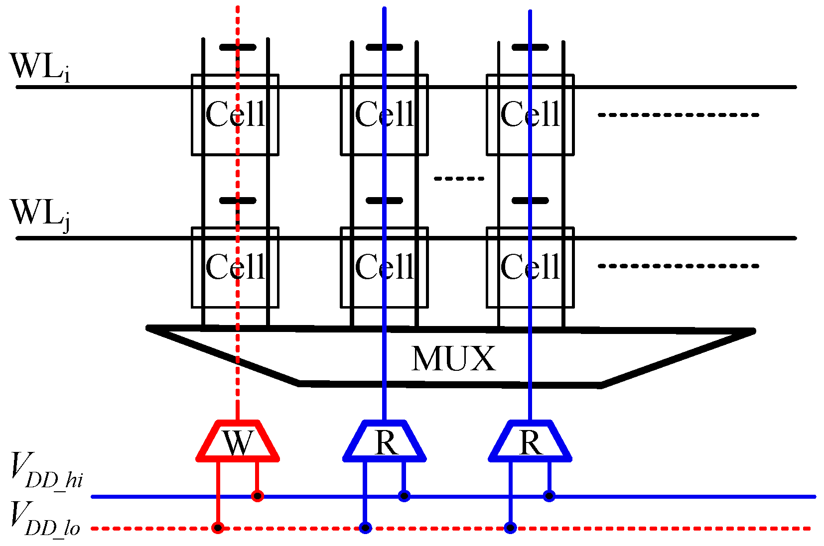
3.1.2. DVS
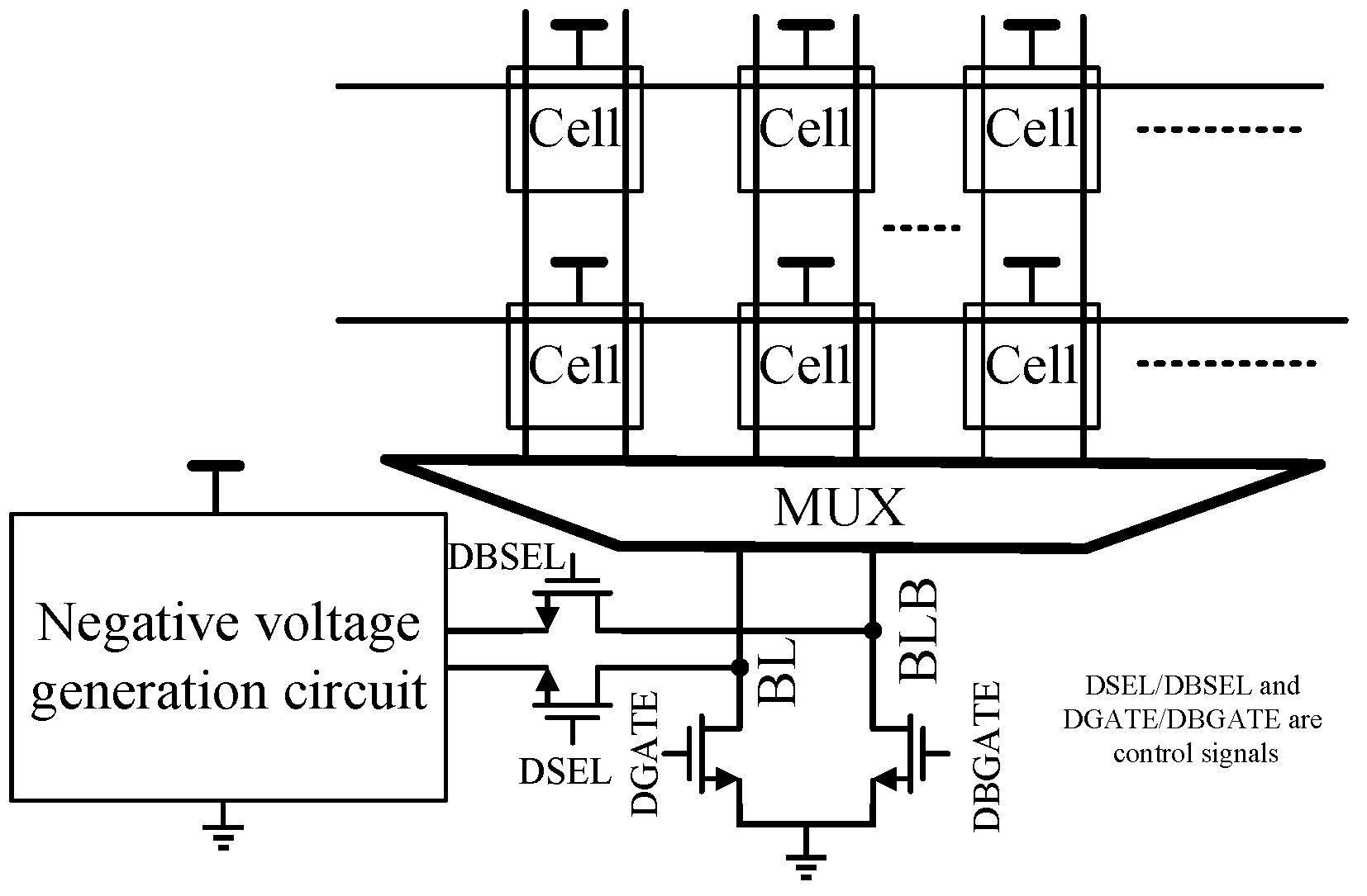
3.1.3. NBL
3.1.4. ABB
3.1.5. Comparison of Different Reliability Enhancement Techniques
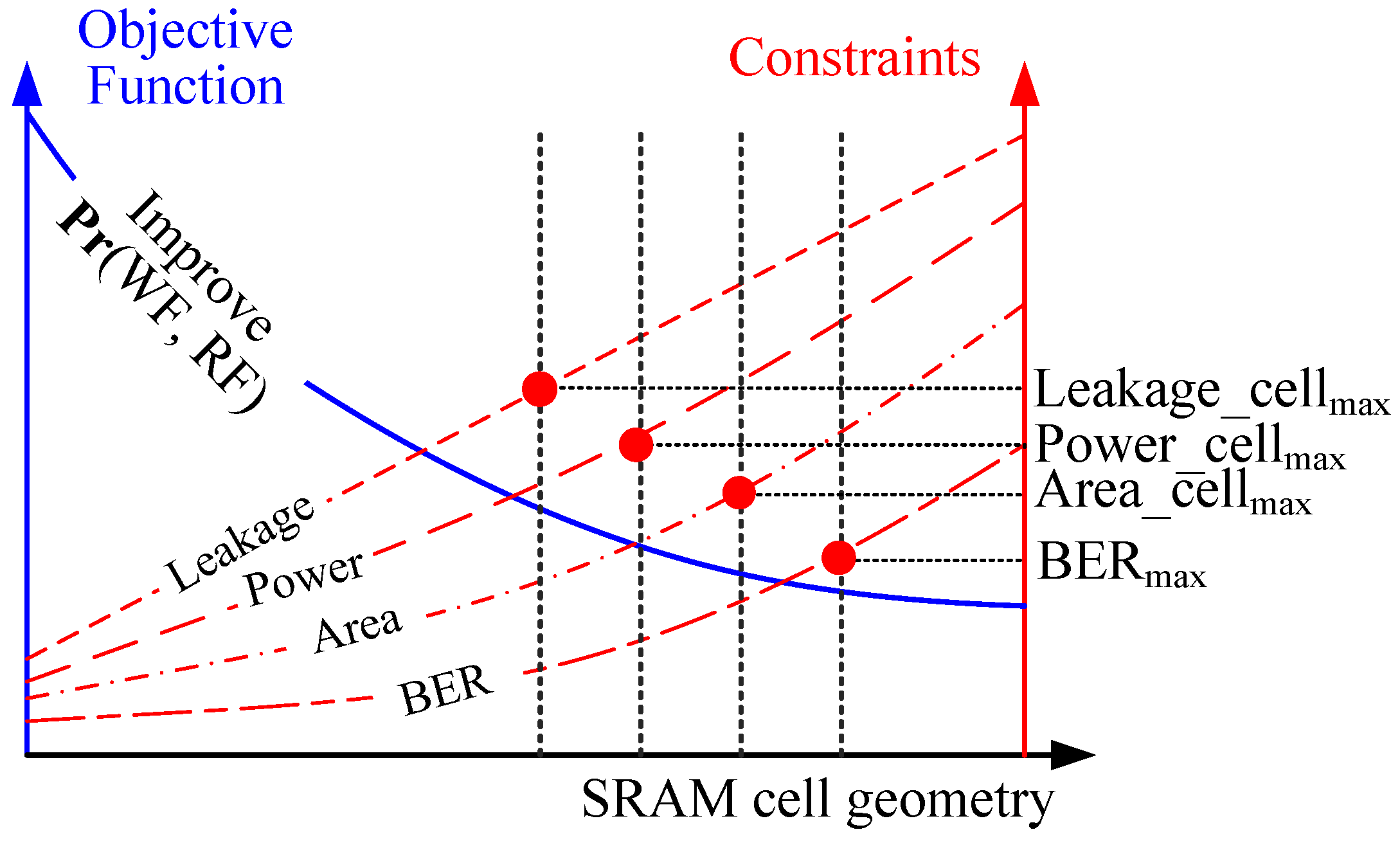
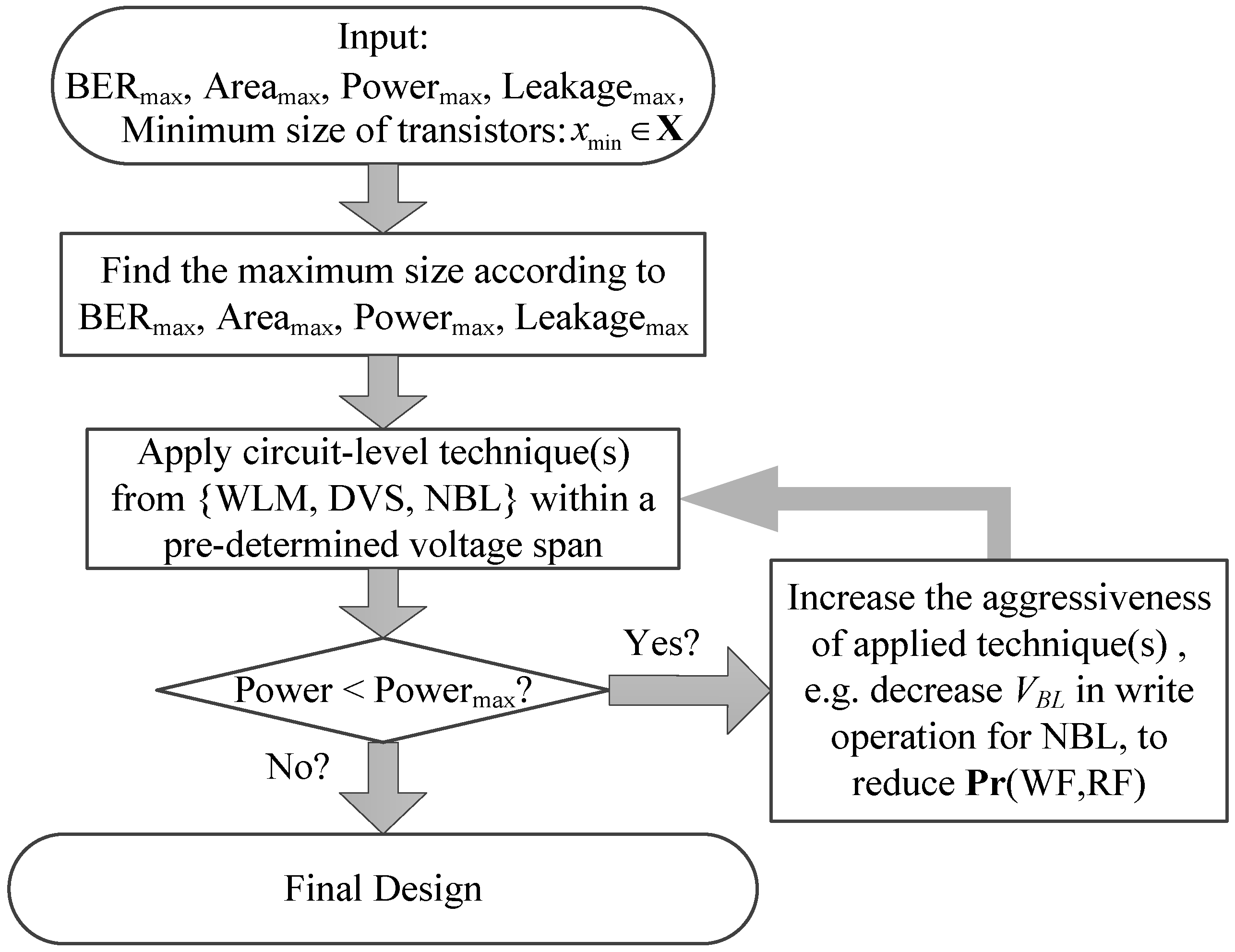
3.2. Problem Formulation
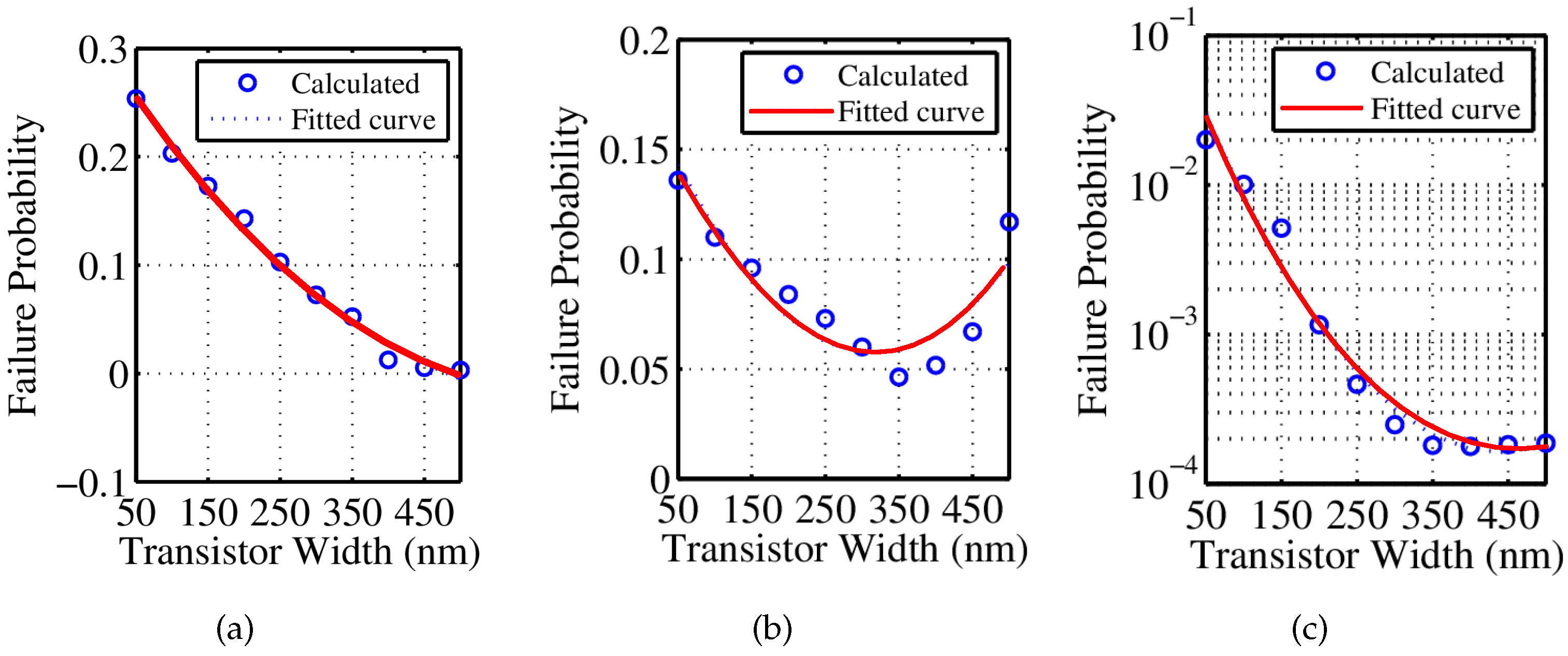
3.2.1. Failure Probability
3.2.2. Reliability
3.2.3. Area
3.2.4. Power Consumption
4. Simulation Results and Discussions
4.1. Uniqueness
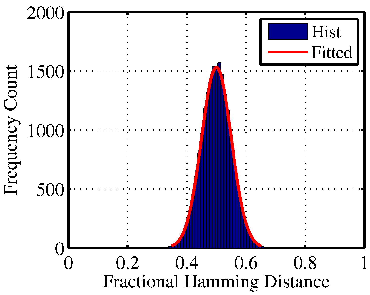
4.2. Randomness
5. Conclusions
Acknowledgments
Author Contributions
Conflicts of Interest
References
- Suh, G.; Devadas, S. Physical Unclonable Functions for Device Authentication and Secret Key Generation. In Proceedings of the 44th ACM/IEEE Design Automation Conference, San Diego, CA, USA, 4–8 June 2007; pp. 9–14.
- Holcomb, D.; Burleson, W.; Fu, K. Power-Up SRAM State as an Identifying Fingerprint and Source of True Random Numbers. IEEE Trans. Comput. 2009, 58, 1198–1210. [Google Scholar] [CrossRef]
- Zhang, L.; Kong, Z.H.; Chang, C.H. PCKGen: A Phase Change Memory based cryptographic key generator. In Proceedings of the 2013 IEEE International Symposium on Circuits and Systems (ISCAS2013), Beijing, China, 19–23 May 2013; pp. 1444–1447.
- Van Aubel, P.; Bernstein, D.J.; Niederhagen, R. Investigating SRAM PUFs in large CPUs and GPUs. In Security, Privacy, and Applied Cryptography Engineering; Springer International Publishing: Cham, Switzerland, 2015; pp. 228–247. [Google Scholar]
- Chellappa, S.; Clark, L.T. SRAM-Based Unique Chip Identifier Techniques. IEEE Trans. Very Large Scale Integr. (VLSI) Syst. 2016, 24, 1213–1222. [Google Scholar] [CrossRef]
- Zimmer, B.; Toh, S.O.; Vo, H.; Lee, Y.; Thomas, O.; Asanovic, K.; Nikolic, B. SRAM assist techniques for operation in a wide voltage range in 28-nm CMOS. IEEE Trans. Circuits Syst. II: Express Briefs 2012, 59, 853–857. [Google Scholar] [CrossRef]
- Zhang, L.; Chang, C.H.; Kong, Z.H.; Liu, C.Q. Statistical analysis and design of 6T SRAM cell for physical unclonable function with dual application modes. In Proceedings of the 2015 IEEE International Symposium on Circuits and Systems (ISCAS2015), Lisbon, Portugal, 24–27 May 2015; pp. 1410–1413.
- Vatajelu, E.I.; Natale, G.D.; Prinetto, P. Towards a highly reliable SRAM-based PUFs. In Proceedings of the Design, Automation and Test Europe Conference (DATE), Dresden, Germany, 14–18 March 2016; pp. 273–276.
- Calhoun, B.H.; Chandrakasan, A.P. Static noise margin variation for sub-threshold SRAM in 65-nm CMOS. IEEE J. Solid-State Circuits 2006, 41, 1673–1679. [Google Scholar] [CrossRef]
- Orshansky, M.; Nassif, S.; Boning, D. Design for Manufacturability and Statistical Design: A Constructive Approach; Springer Science & Business Media: New York, NY, USA, 2008. [Google Scholar]
- Synopsys, Inc. HSPICE® User Guide: RF Analysis; Mountain View, CA, USA, 2010. [Google Scholar]
- Chellappa, S.; Dey, A.; Clark, L. Improved circuits for microchip identification using SRAM mismatch. In Proceedings of the 2011 IEEE Custom Integrated Circuits Conference (CICC), San Jose, CA, USA, 19–21 September 2011; pp. 1–4.
- Agarwal, K.; Nassif, S. Statistical analysis of SRAM cell stability. In Proceedings of the 43rd ACM/IEEE Design Automation Conference, San Francisco, CA, USA, 24–28 July 2006; pp. 57–62.
- Mukhopadhyay, S.; Mahmoodi, H.; Roy, K. Modeling of failure probability and statistical design of SRAM array for yield enhancement in nanoscaled CMOS. IEEE Trans. Comput.-Aided Des. Integr. Circuits Syst. 2005, 24, 1859–1880. [Google Scholar] [CrossRef]
- Alorda, B.; Carmona, C.; Bota, S. Word-line power supply selector for stability improvement of embedded SRAMs in high reliability applications. In Proceedings of the 2014 Design, Automation Test in Europe Conference Exhibition (DATE), Dresden, Germany, 24–28 March 2014; pp. 1–6.
- Zhang, K.; Bhattacharya, U.; Chen, Z.; Hamzaoglu, F.; Murray, D.; Vallepalli, N.; Wang, Y.; Zheng, B.; Bohr, M. A 3-GHz 70-Mb SRAM in 65-nm CMOS technology with integrated column-based dynamic power supply. IEEE J. Solid-State Circuits 2006, 41, 146–151. [Google Scholar] [CrossRef]
- Sinangil, M.E.; Poulton, J.W.; Fojtik, M.R.; Greer, T.H., III; Tell, S.G.; Gotterba, A.J.; Wang, J.; Golbus, J.; Zimmer, B.; Dally, W.J.; et al. A 28 nm 2 Mbit 6T SRAM With Highly Configurable Low-Voltage Write-Ability Assist Implementation and Capacitor-Based Sense-Amplifier Input Offset Compensation. IEEE J. Solid-State Circuits 2016, 51, 557–567. [Google Scholar]
- Mukhopadhyay, S.; Mahmoodi, H.; Roy, K. Reduction of Parametric Failures in Sub-100-nm SRAM Array Using Body Bias. IEEE Trans. Comput.-Aided Des. Integr. Circuits Syst. 2008, 27, 174–183. [Google Scholar] [CrossRef]
- Hokazono, A.; Balasubramanian, S.; Ishimaru, K.; Ishiuchi, H.; Liu, T.J.K.; Hu, C. MOSFET design for forward body biasing scheme. IEEE Electron. Dev. Lett. 2006, 27, 387–389. [Google Scholar] [CrossRef]
- Mostafa, H.; Anis, M.; Elmasry, M. Adaptive Body Bias for Reducing the Impacts of NBTI and Process Variations on 6T SRAM Cells. IEEE Trans. Circuits Syst. I Reg. Pap. 2011, 58, 2859–2871. [Google Scholar] [CrossRef]
- Wang, J.; Nalam, S.; Calhoun, B.H. Analyzing static and dynamic write margin for nanometer SRAMs. In Proceedings of the 2008 ACM/IEEE International Symposium on Low Power Electronics and Design (ISLPED), Bangalore, India, 11–13 August 2008; pp. 129–134.
- Lin, S.; Costello, D. Error Control Coding; Prentice-Hall: Englewood Cliffs, NJ, USA, 2004. [Google Scholar]
- Bösch, C.; Guajardo, J.; Sadeghi, A.R.; Shokrollahi, J.; Tuyls, P. Efficient helper data key extractor on FPGAs. In Proceedings of the Workshop on Cryptographic Hardware and Embedded Systems, Washington, DC, USA, 10–13 August 2008; pp. 181–197.
- Maiti, A.; Casarona, J.; McHale, L.; Schaumont, P. A large scale characterization of RO-PUF. In Proceedings of the 2010 IEEE International Symposium on Hardware-Oriented Security and Trust (HOST), Anaheim, CA, USA, 13–14 June 2010; pp. 94–99.
- Cao, Y.; Zhang, L.; Chang, C.H.; Chen, S. A Low-Power Hybrid RO PUF With Improved Thermal Stability for Lightweight Applications. IEEE Trans. Comput.-Aided Des. Integr. Circuits Syst. 2015, 34, 1143–1147. [Google Scholar]


| Technique | Column-Based | S(Read) | S(Write) | Other Drawbacks |
|---|---|---|---|---|
| WLM | × | 0 | - | |
| DVS | √ | - | ||
| NBL | √ | 0 | - | |
| ABB (NMOS only) | × | Triple-well process, Large area overhead | ||
| ABB (PMOS only) | × | |||
| ABB (Both MOSFETs) | × |
| Description | Design | X | M | BER | Area | Leakage | Power | |||
|---|---|---|---|---|---|---|---|---|---|---|
| Single-mode PUF | 1 | 140 | ||||||||
| Single-mode memory | 2 | 405 | ||||||||
| Dual-mode SPUF | 3 | 158 | ||||||||
| 4 | 154 | |||||||||
| 5 | 143 | |||||||||
| 6 | 155 | |||||||||
| Dual-mode RO PUF | 7 | − | − | − | − | − |
| Test Description | Passed/Total | P-value | Pass? |
|---|---|---|---|
| Frequency | 98/100 | 0.145 | √ |
| Block Frequency () | 100/100 | 0.262 | √ |
| Cusum-Forward | 98/100 | 0.249 | √ |
| Cusum-Reverse | 99/100 | 0.817 | √ |
| Runs | 97/100 | 0.102 | √ |
| Longest Run of Ones | 98/100 | 0.868 | √ |
| Rank | 100/100 | 0.015 | √ |
| Spectral DFT | 100/100 | 0.024 | √ |
| Non-overlapping Templates () | 99/100 | 0.367 | √ |
| Overlapping Templates () | 99/100 | 0.898 | √ |
| Approximate Entropy | 98/100 | 0.475 | √ |
| Linear Complexity () | 96/100 | 0.035 | √ |
| Serial | 100/100 | 0.038 | √ |
© 2016 by the authors; licensee MDPI, Basel, Switzerland. This article is an open access article distributed under the terms and conditions of the Creative Commons Attribution (CC-BY) license (http://creativecommons.org/licenses/by/4.0/).
Share and Cite
Chang, C.-H.; Liu, C.Q.; Zhang, L.; Kong, Z.H. Sizing of SRAM Cell with Voltage Biasing Techniques for Reliability Enhancement of Memory and PUF Functions. J. Low Power Electron. Appl. 2016, 6, 16. https://doi.org/10.3390/jlpea6030016
Chang C-H, Liu CQ, Zhang L, Kong ZH. Sizing of SRAM Cell with Voltage Biasing Techniques for Reliability Enhancement of Memory and PUF Functions. Journal of Low Power Electronics and Applications. 2016; 6(3):16. https://doi.org/10.3390/jlpea6030016
Chicago/Turabian StyleChang, Chip-Hong, Chao Qun Liu, Le Zhang, and Zhi Hui Kong. 2016. "Sizing of SRAM Cell with Voltage Biasing Techniques for Reliability Enhancement of Memory and PUF Functions" Journal of Low Power Electronics and Applications 6, no. 3: 16. https://doi.org/10.3390/jlpea6030016