
A 4.1 W/mm2 Hybrid Inductive/Capacitive Converter for 2–140 mA-DVS Load under Inductor †

Abstract
:1. Introduction
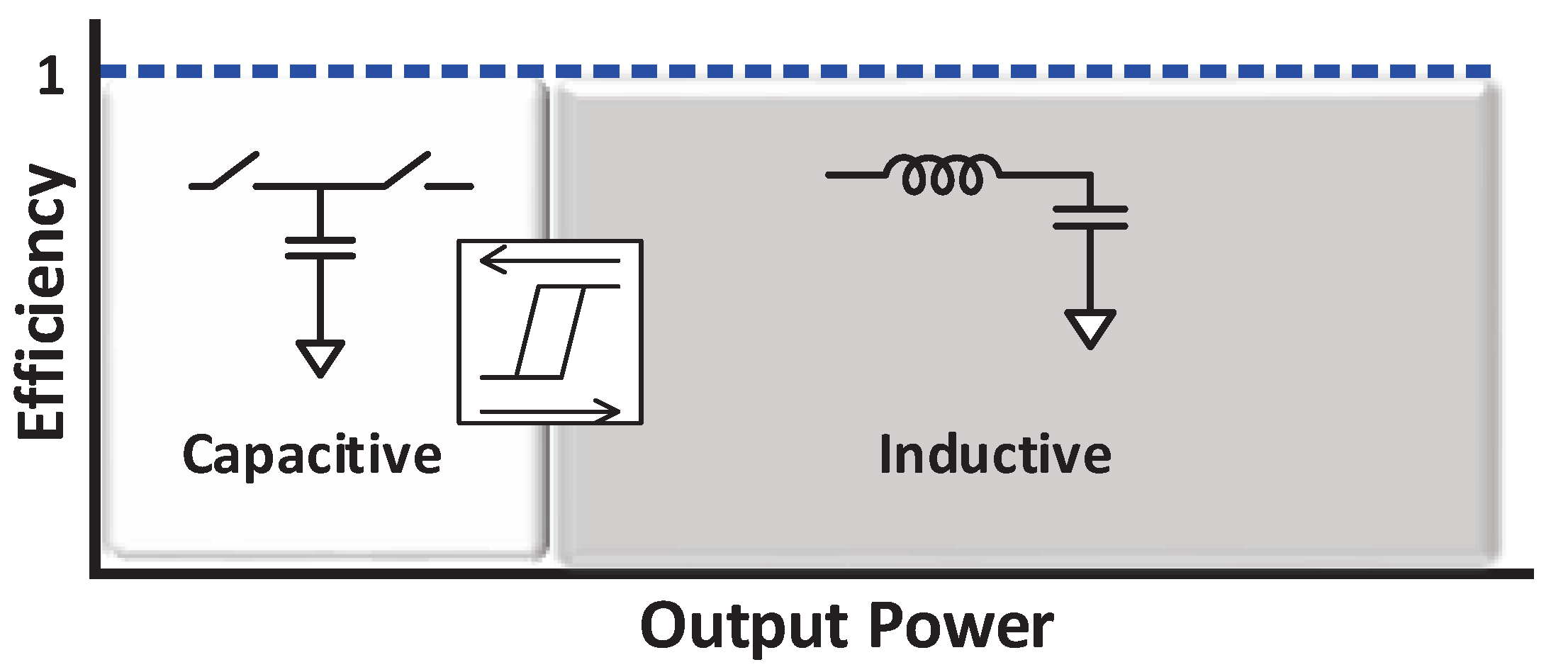
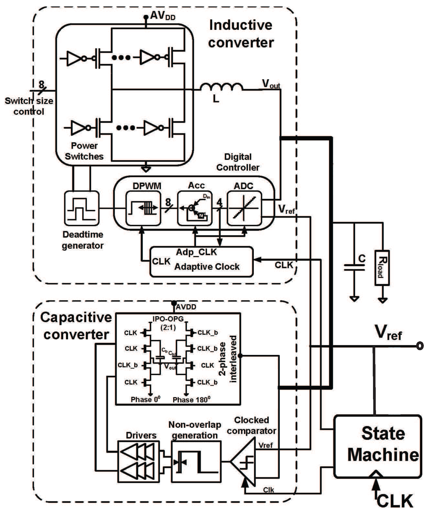
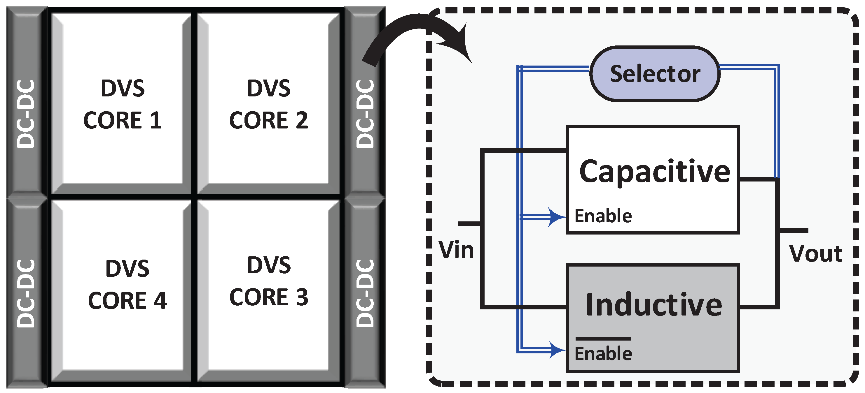
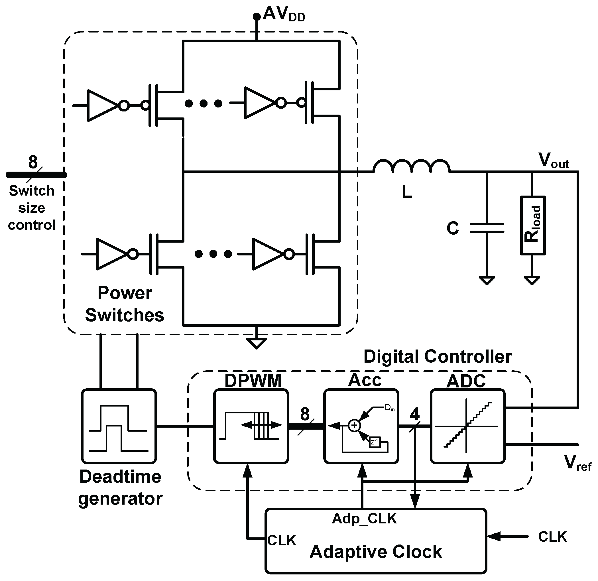
2. Architecture
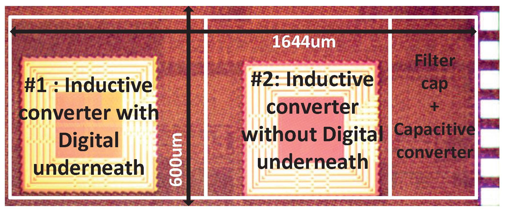
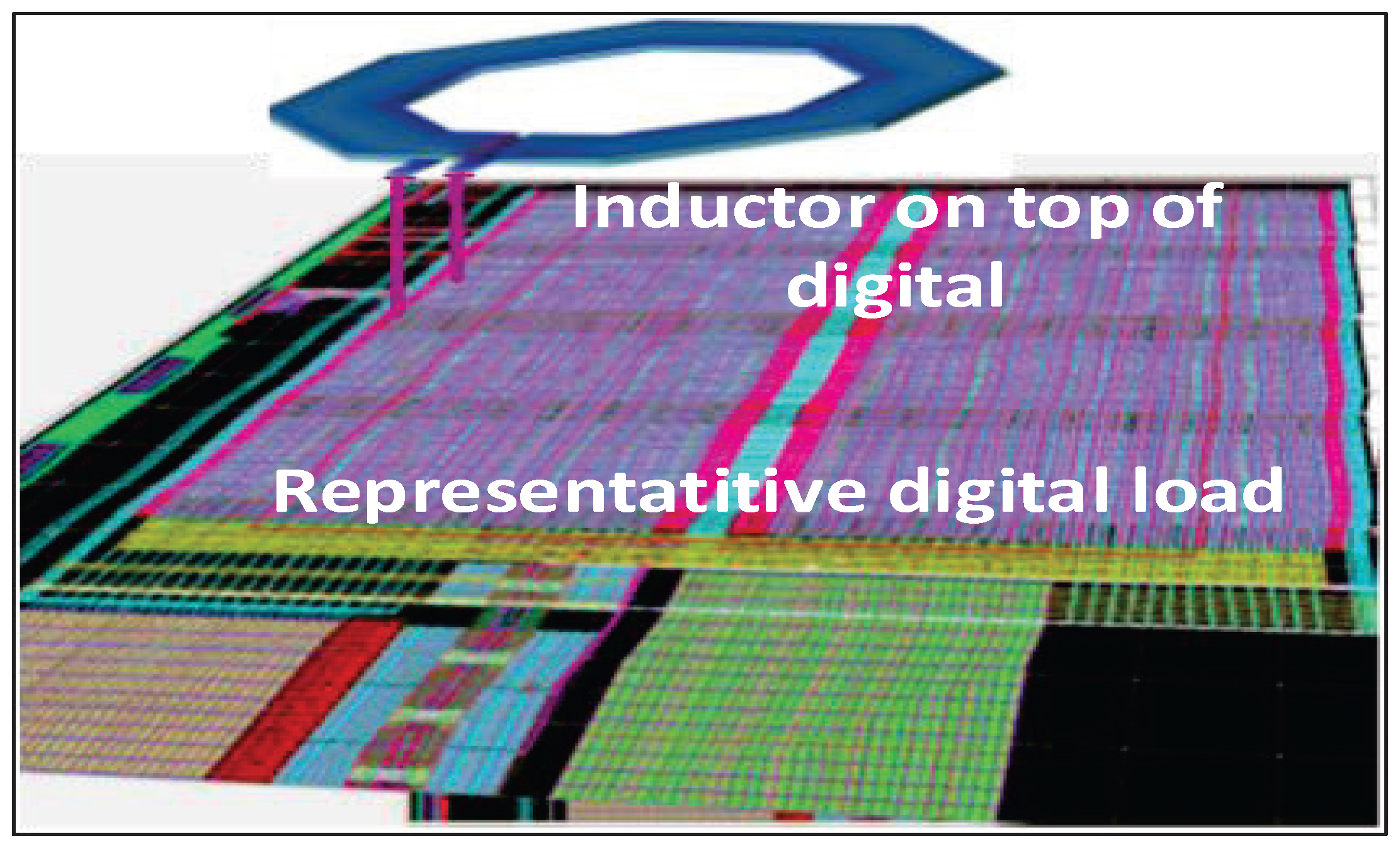
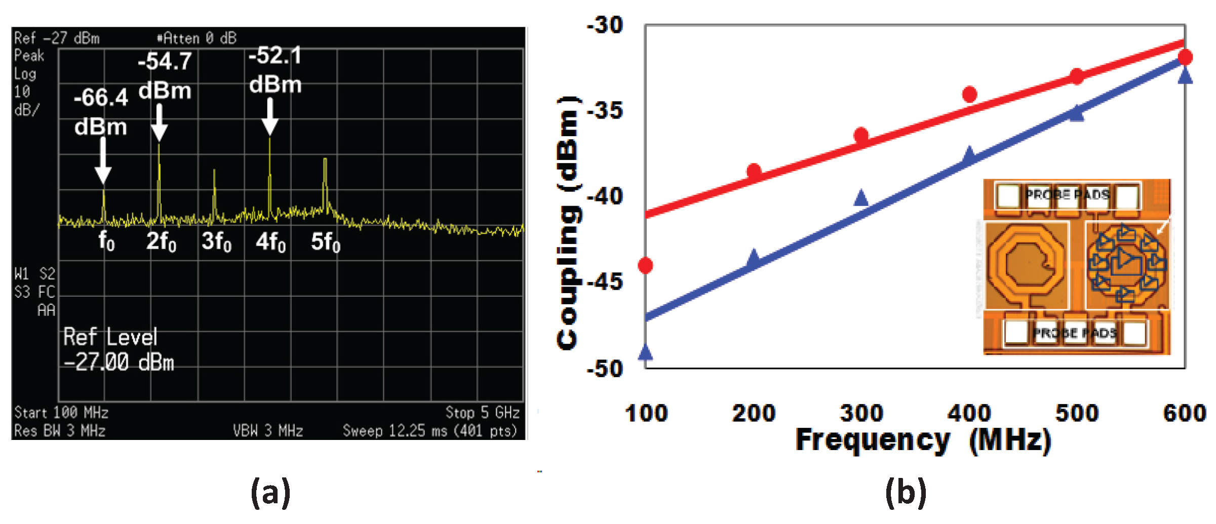
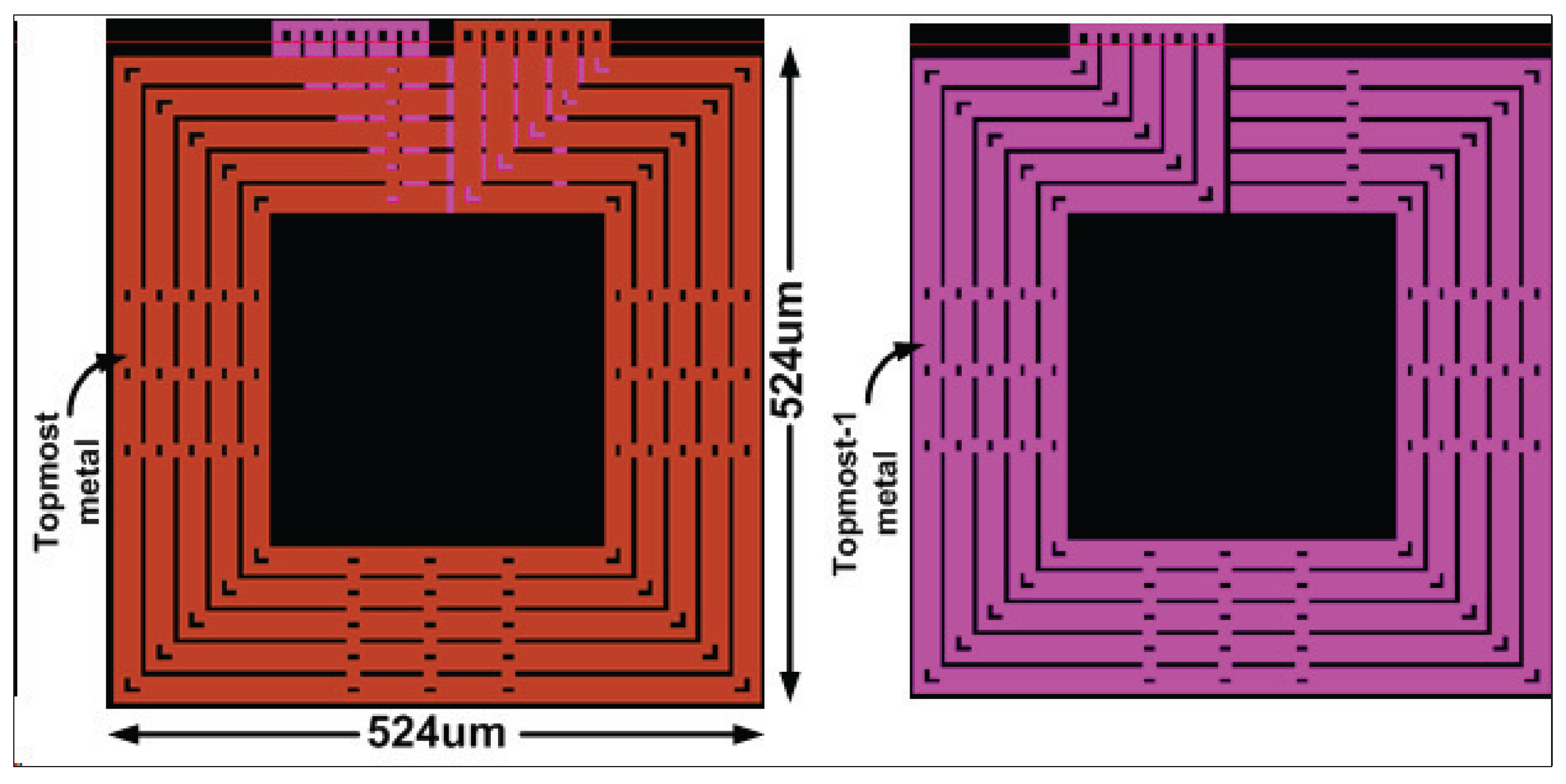
2.1. Digital under Inductor—Proof of Concept
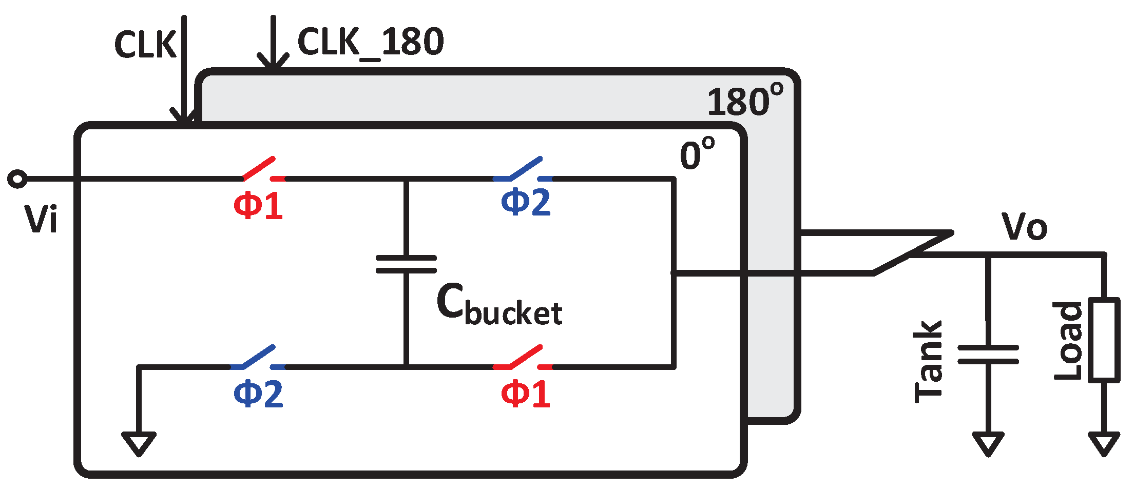
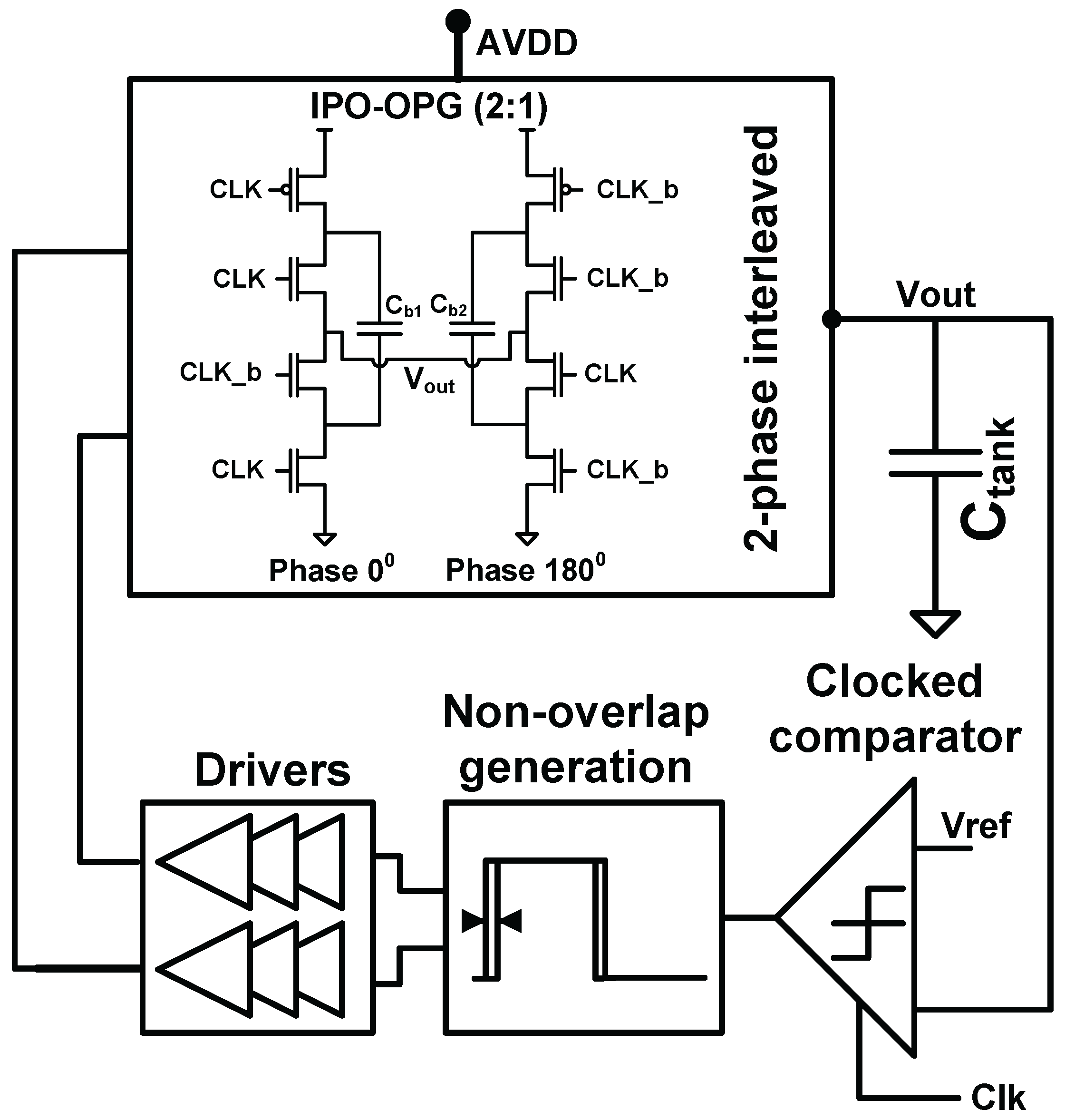
2.2. Capacitive Converter
2.3. Inductive Converter
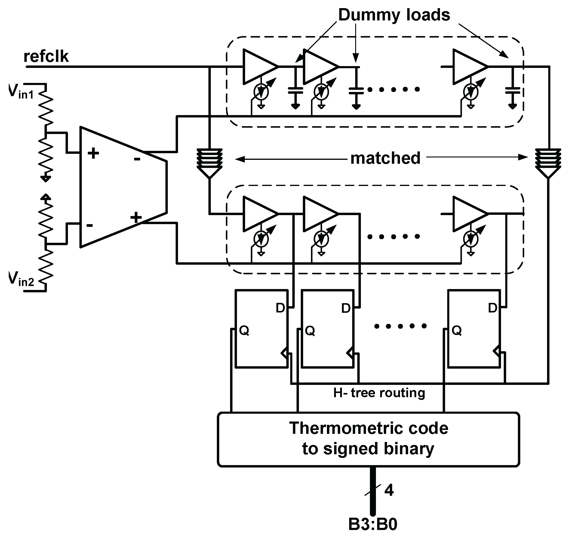
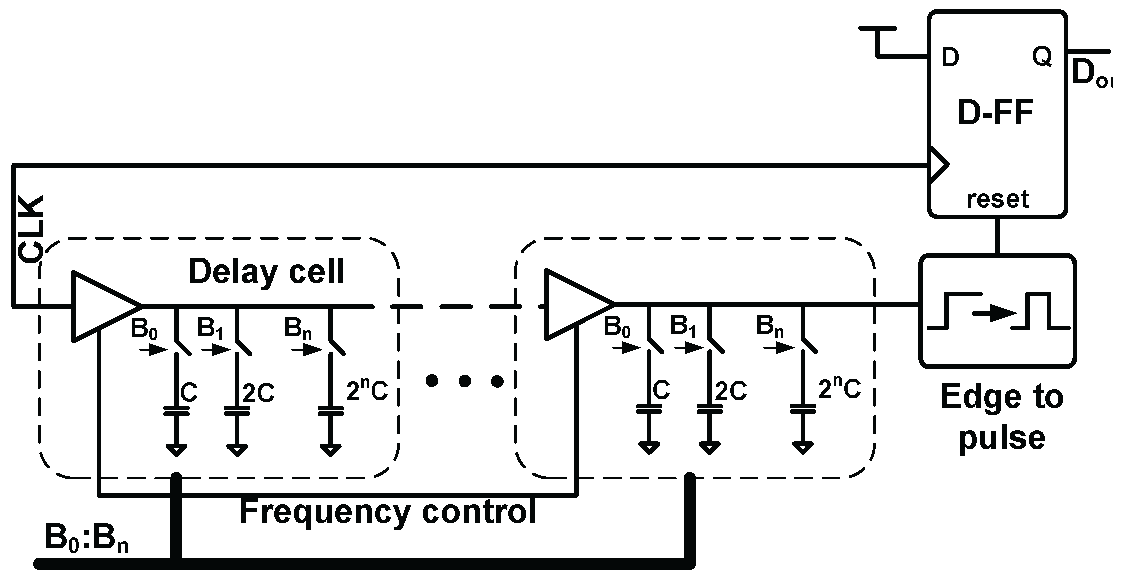
2.3.1. Time Based Analog to Digital Converter (TDC)
2.3.2. Accumulator
2.3.3. Digital Pulse Width Modulator
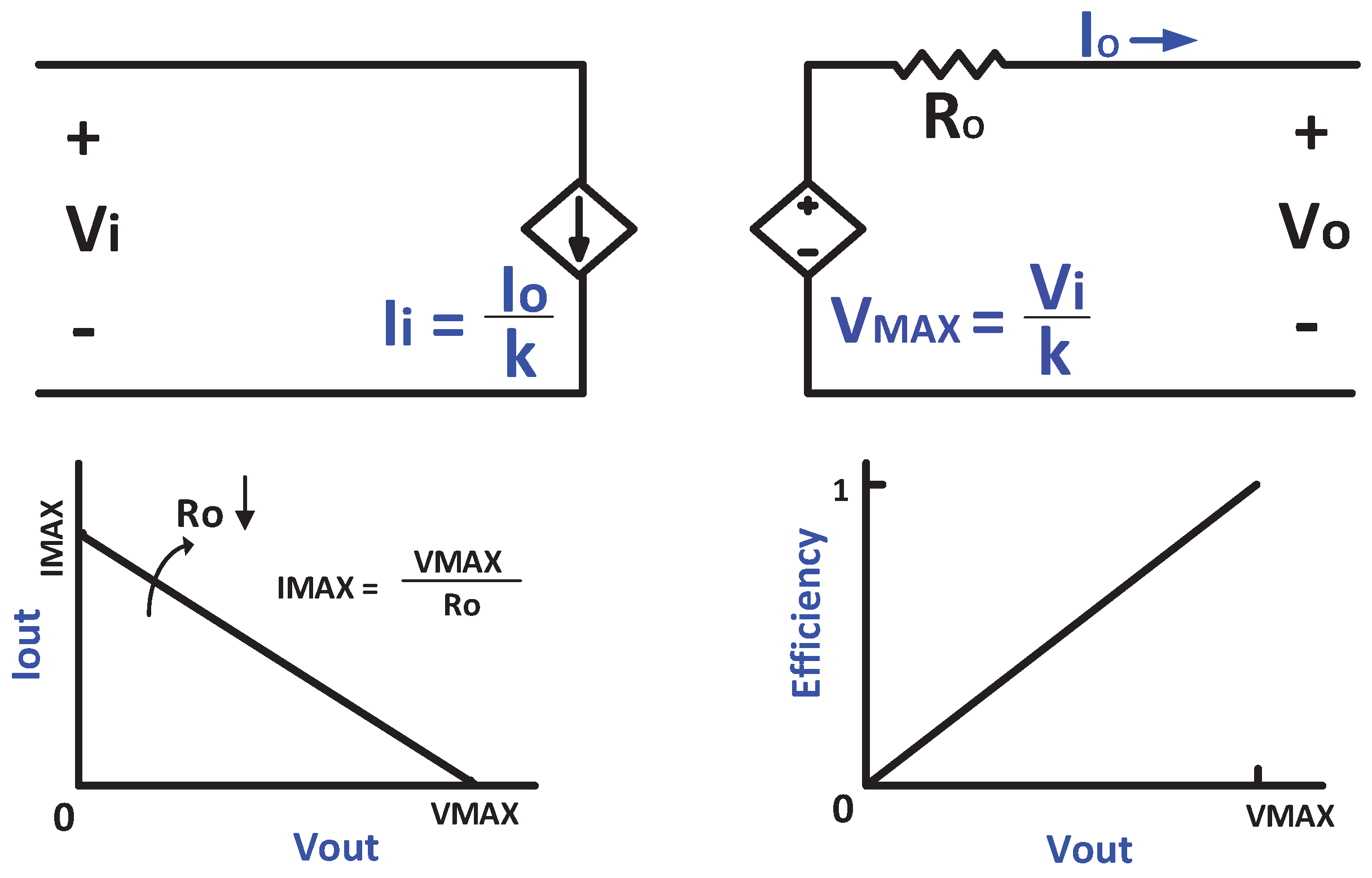
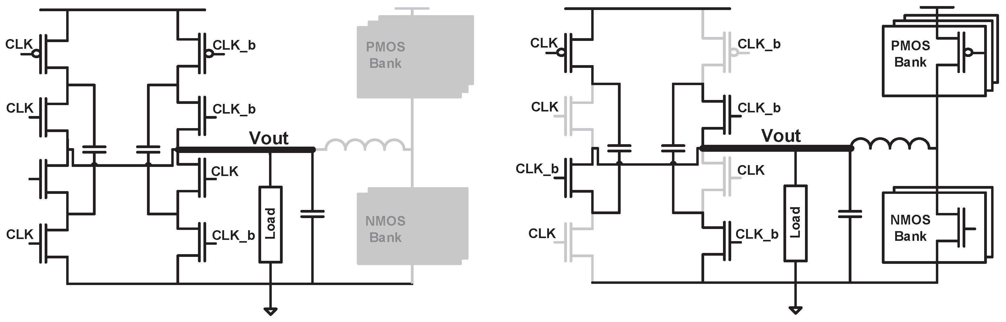
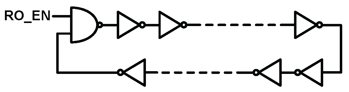
2.3.4. Efficiency Improvement Techniques
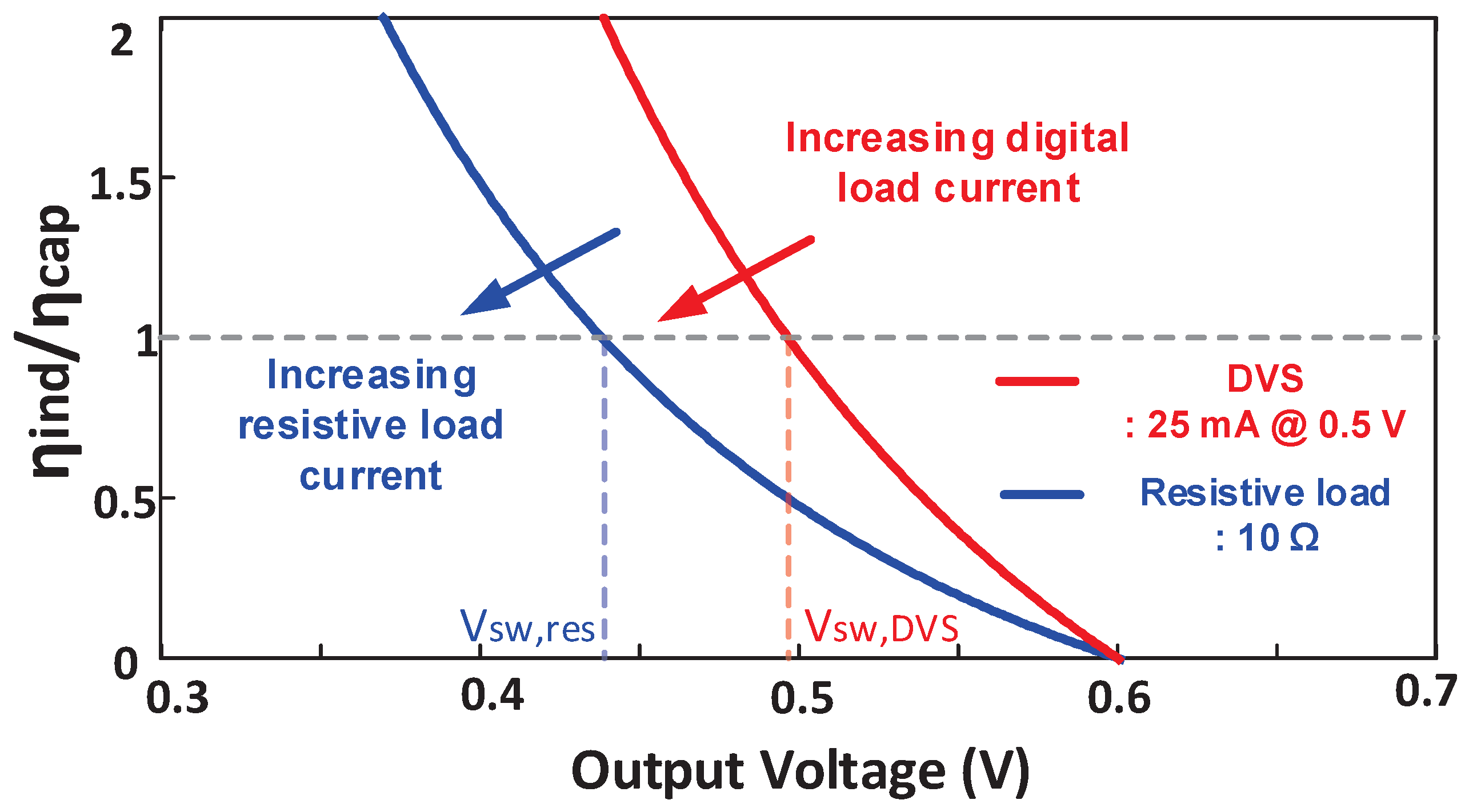
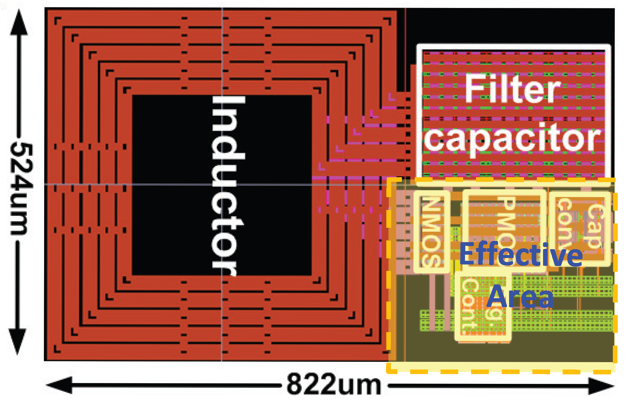
2.4. Combined Converter Design
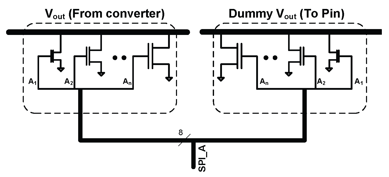
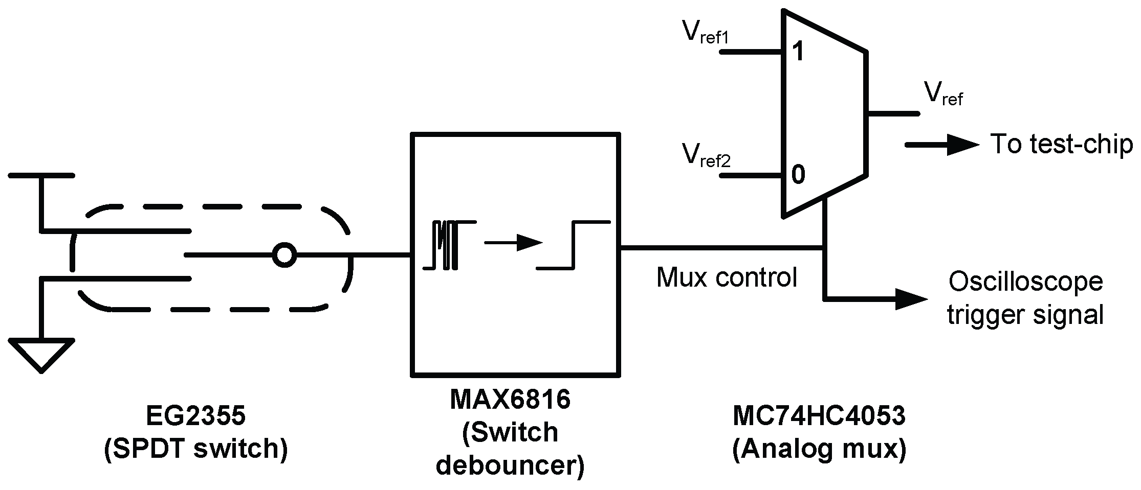
3. Measurement Test Setup
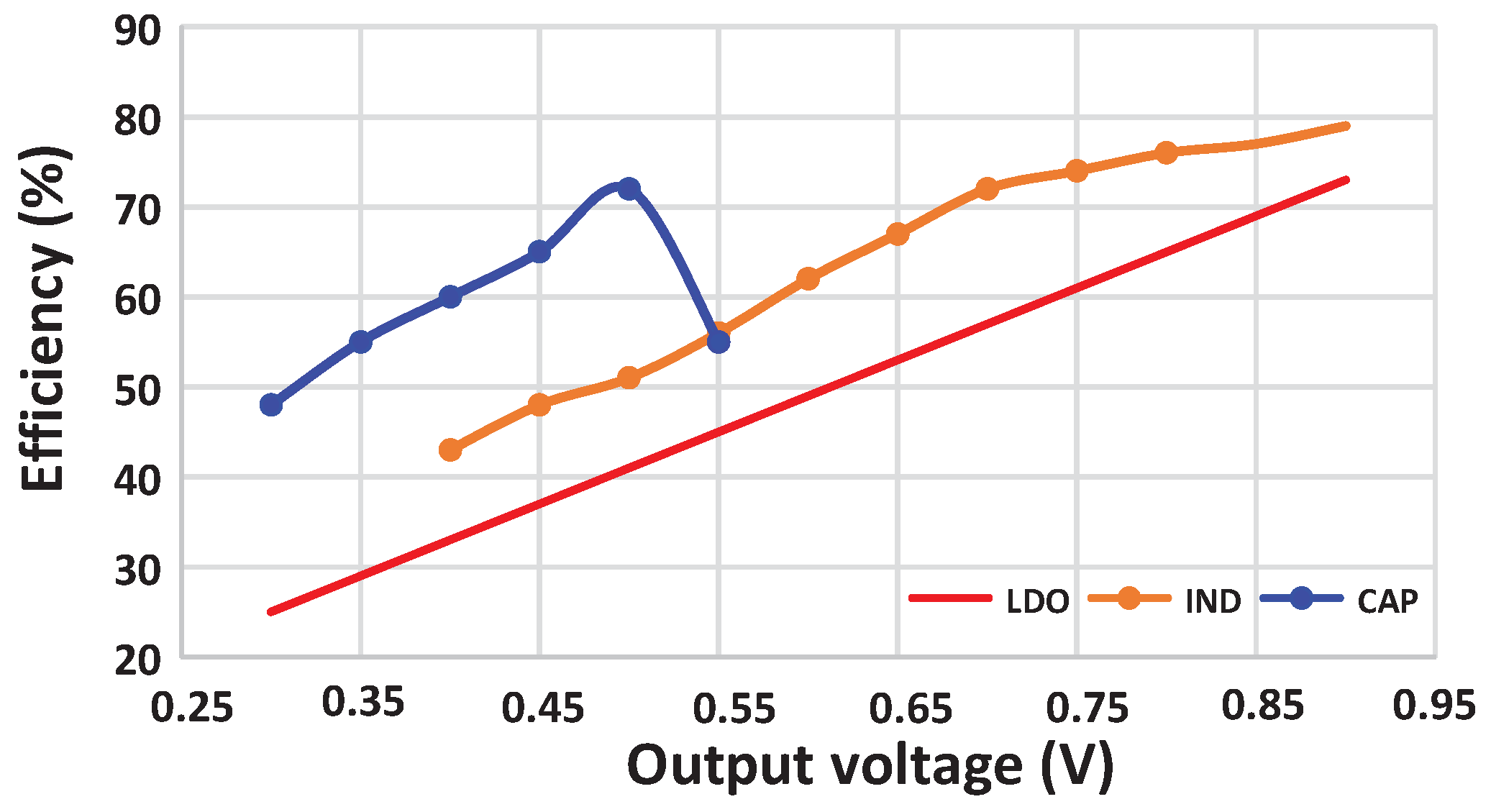
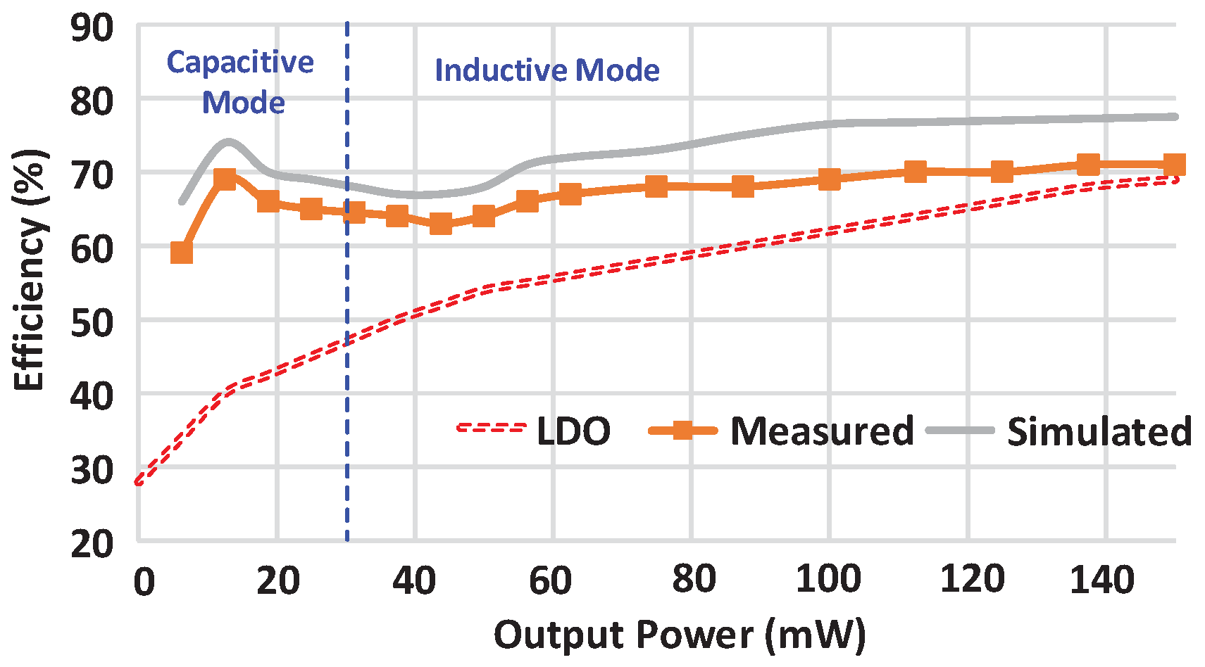
3.1. Steady State Efficiency
3.2. Load Transient Measurement
3.3. Transient Measurement
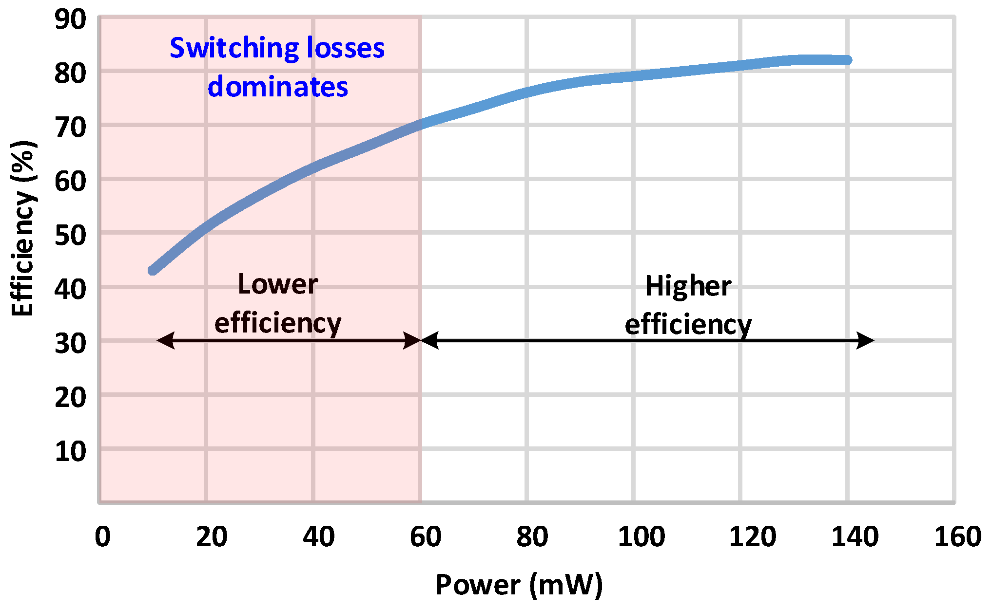
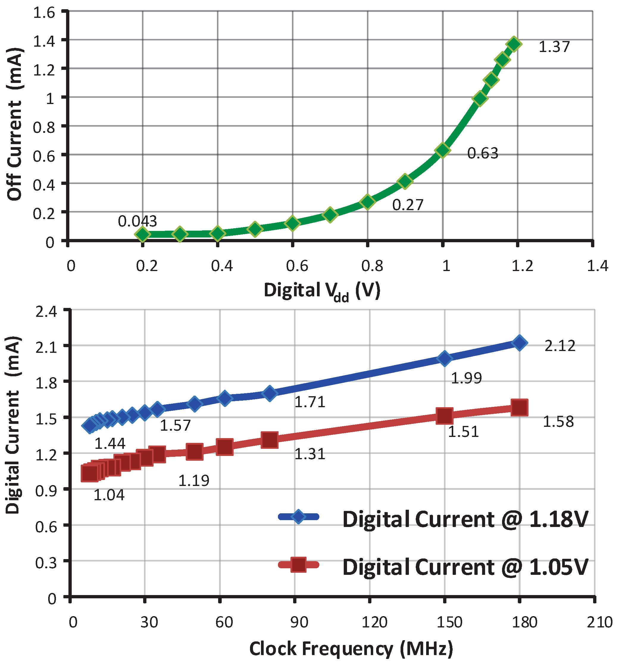
4. Measurement Results
5. Conclusions
Acknowledgments
Author Contributions
Conflicts of Interest
References
- Roadmap, I.T.R.S. International Technology Roadmap for Semiconductors; Semiconductor Industry Association: Washington, DC, USA, 2009. [Google Scholar]
- Kaul, H.; Anders, M.; Mathew, S.; Hsu, S.; Agarwal, A.; Krishnamurthy, R.; Borkar, S. A 320 mV 56 uW 411 GOPS/Watt ultra-low voltage motion estimation accelerator in 65 nm CMOS. In Proceedings of the IEEE International Solid-State Circuits Conference (ISSCC 2008), Digest of Technical Papers, San Francisco, CA, USA, 3–7 February 2008; pp. 316–616.
- Kudva, S.; Harjani, R. Fully-integrated on-chip DC-DC converter with a 450× output range. IEEE J. Solid-State Circuits 2011, 46, 1940–1951. [Google Scholar] [CrossRef]
- Urard, P.; Paumier, L.; Heinrich, V.; Raina, N.; Chawla, N. A 360 mw 105 Mb/s DVB-S2 compliant codec based on 64800b LDPC and BCH codes enabling satellite-transmission portable devices. In Proceedings of the IEEE International Solid-State Circuits Conference (ISSCC 2008), Digest of Technical Papers, San Francisco, CA, USA, 3–7 February 2008; pp. 310–311.
- Calhoun, B.; Chandrakasan, A. Standby power reduction using dynamic voltage scaling and canary flip-flop structures. IEEE Solid-State Circuits 2004, 39, 1504–1511. [Google Scholar] [CrossRef]
- Semeraro, G.; Magklis, G.; Balasubramonian, R.; Albonesi, D.; Dwarkadas, S.; Scott, M. Energy-efficient processor design using multiple clock domains with dynamic voltage and frequency scaling. In Proceedings of the IEEE 8th International Symposium on High Performance Computer Architecture, Cambridge, MA, USA, 2–6 February 2002; pp. 29–40.
- Kim, W.; Gupta, M.S.; Wei, G.-Y.; Brooks, D. System level analysis of fast, per-core DVFS using on-chip switching regulators. In Proceedings of the IEEE 14th International Symposium on High Performance Computer Architecture, Salt Lake City, UT, USA, 16–20 February 2008; pp. 123–134.
- Le, H.-P.; Sanders, S.; Alon, E. Design techniques for fully integrated switched-capacitor DC-DC converters. IEEE J. Solid-State Circuits 2011, 46, 2120–2131. [Google Scholar] [CrossRef]
- Wibben, J.; Harjani, R. A high-efficiency DC DC converter using 2nH integrated inductors. IEEE J. Solid-State Circuits 2008, 43, 844–854. [Google Scholar] [CrossRef]
- Bassi, G.; Colalongo, L.; Richelli, A.; Kovacs-Vajna, Z. A 150 mV–1.2 V fully-integrated DC-DC converter for Thermal Energy Harvesting. In Proceedings of the 2012 International Symposium on Power Electronics, Electrical Drives, Automation and Motion (SPEEDAM), Sorrento, Italy, 20–22 June 2012; pp. 331–334.
- Richelli, A.; Colalongo, L.; Quarantelli, M.; Carmina, M.; Kovacs-Vajna, Z.M. A fully integrated inductor-based 1.8-6-V step-up converter. IEEE J. Solid-State Circuits 2004, 39, 242–245. [Google Scholar] [CrossRef]
- Savio, A.; Carmina, M.; Richelli, A.; Colalongo, L.; Kovacs-Vajna, Z.M. A new lumped model for on-chip inductors including substrate currents. In Proceedings of the 15th International Conference on Microelectronics (ICM 2003), Cairo, Egypt, 11 December 2003; pp. 180–183.
- Lhermet, H.; Condemine, C.; Plissonnier, M.; Salot, R.; Audebert, P.; Rosset, M. Efficient Power Management Circuit: Thermal Energy Harvesting to Above-IC Microbattery Energy Storage. In Proceedings of the 2007 IEEE International Solid-State Circuits Conference, Digest of Technical Papers, San Francisco, CA, USA, 11–15 February 2007; pp. 62–587.
- Chen, P.H.; Koichi, I.; Katsuyuki, I.; Zhang, X.; Honda, K.; Okuma, Y.; Ryu, Y.; Takamiya, M.; Sakurai, T. Startup Techniques for 95 mV Step-Up Converter by Capacitor Pass-On Scheme and Vth-Tuned Oscillator With Fixed Charge Programming. IEEE J. Solid-State Circuits 2012, 47, 1252–1260. [Google Scholar] [CrossRef]
- Sturcken, N.; OSullivan, E.J.; Wang, N.; Herget, P.; Webb, B.C.; Romankiw, L.T.; Petracca, M.; Davies, R.; Fontana, R.E., Jr.; Decad, G.M.; et al. A 2.5D integrated voltage regulator using coupled-magnetic-core inductors on silicon interposer. IEEE J. Solid-State Circuits 2013, 48, 244–254. [Google Scholar] [CrossRef]
- Kurd, N.; Chowdhury, M.; Burton, E.; Thomas, T.P.; Mozak, C.; Boswell, B.; Lal, M.; Deval, A.; Douglas, J.; Elassal, M.; et al. Haswell: A family of IA 22 nm processors. In Proceedings of the IEEE International Solid-State Circuits Conference (ISSCC 2014), Digest of Technical Papers, Montgomery Village, MD, USA, 9–13 February 2014; pp. 112–114.
- Andersen, T.; Krismer, F.; Kolar, J.; Toifl, T.; Menolfi, C.; Kull, L.; Morf, T.; Kossel, M.; Brandli, M.; Buchmann, P.; et al. A sub-ns response on-chip switched-capacitor DC-DC voltage regulator delivering 3.7 W/mm2 at 90% efficiency using deep-trench capacitors in 32 nm soi CMOS. In Proceedings of the IEEE International Solid-State Circuits Conference (ISSCC 2014), Digest of Technical Papers, Montgomery Village, MD, USA, 9–13 February 2014; pp. 90–91.
- Chang, L.; Montoye, R.; Ji, B.; Weger, A.; Stawiasz, K.; Dennard, R. A fully-integrated switched-capacitor 2:1 voltage converter with regulation capability and 90% efficiency at 2.3 A/mm2. In Proceedings of the 2010 IEEE Symposium on VLSI Circuits (VLSIC), Honolulu, HI, USA, 16–18 June 2010; pp. 55–56.
- Kudva, S.; Chaubey, S.; Harjani, R. High power-density, hybrid inductive/capacitive converter with area reuse for multi-domain DVS. In Proceedings of the 2014 IEEE Custom Integrated Circuits Conference (CICC), San Jose, CA, USA, 15–17 September 2014; pp. 1–4.
- Richelli, A.; Colalongo, L.; Tonoli, S.; Kovacs-Vajna, Z.M. A 0.2–1.2 V DC/DC Boost Converter for Power Harvesting Applications. IEEE Trans. Power Electron. 2009, 24, 1541–1546. [Google Scholar] [CrossRef]
- Richelli, A.; Alessandro, C.; Zsolt, K.-V. Design of Hybrid Low Voltage DC/DC Converters Based on Power Efficiency. J. Low Power Electron. 2013, 9, 97–102. [Google Scholar] [CrossRef]
- Richelli, A.; Colalongo, L.; Zsolt, K.-V. A 30 mV–2.5 V DC/DC converter for energy harvesting. J. Low Power Electron. 2015, 11, 190–195. [Google Scholar] [CrossRef]
- Kudva, S.; Harjani, R. Fully integrated capacitive converter with all digital ripple mitigation. In Proceedings of the 2012 IEEE Custom Integrated Circuits Conference (CICC), San Jose, CA, USA, 9–12 September 2012; pp. 1–4.
- Yue, C.; Wong, S. On-chip spiral inductors with patterned ground shields for si-based RFICs. IEEE J. Solid-State Circuits 1998, 33, 743–752. [Google Scholar] [CrossRef]
- Harjani, R.; Chaubey, S. A unified framework for capacitive series-parallel DC-DC converter design. In Proceedings of the 2014 IEEE Custom Integrated Circuits Conference (CICC), San Jose, CA, USA, 15–17 September 2014; pp. 1–8.
- Li, G.; Tousi, Y.M.; Hassibi, A.; Afshari, E. Delay-Line-Based Analog-to-Digital Converters. IEEE Trans. Circuits Syst. II Express Briefs 2009, 56, 464–468. [Google Scholar] [CrossRef]
- Mesgarani, A.; Fu, H.P.; Yan, M.; Tekin, A.; Yu, H.; Ay, S.U. A 5-bit 1.25 GS/s 4.7mWdelay-based pipelined ADC in 65 nm CMOS. In Proceedings of the 2013 IEEE International Symposium on Circuits and Systems (ISCAS 2013), Beijing, China, 19–23 May 2013; pp. 2018–2021.
- Musunuri, S.; Chapman, P. Optimization of cmos transistors for low power DC-DC converters. In Proceedings of the IEEE 36th Power Electronics Specialists Conference (PESC ’05), Recife, Brazil, 16 June 2005; pp. 2151–2157.
- Ma, D.; Ki, W.-H.; Ying Tsui, C. An integrated one-cycle control buck converter with adaptive output and dual loops for output error correction. IEEE J. Solid-State Circuits 2004, 39, 140–149. [Google Scholar] [CrossRef]
- Xiao, J.; Peterchev, A.; Zhang, J.; Sanders, S. A 4 uA quiescent-current dual-mode digitally controlled buck converter IC for cellular phone applications. IEEE J. Solid-State Circuits 2004, 39, 2342–2348. [Google Scholar] [CrossRef]
- Abedinpour, S.; Bakkaloglu, B.; Kiaei, S. A multistage interleaved synchronous buck converter with integrated output filter in 0.18 μm sige process. IEEE Trans. Power Electron. 2007, 22, 2164–2175. [Google Scholar] [CrossRef]
- Somasekhar, D.; Srinivasan, B.; Pandya, G.; Hamzaoglu, F.; Khellah, M.; Karnik, T.; Zhang, K. Multi-phase 1 GHz voltage doubler charge-pump in 32 nm logic process. In Proceedings of the 2009 Symposium on VLSI Circuits, Tokyo, Japan, 16–18 June 2009; pp. 196–197.
- Lee, H.; Mok, P. An SC voltage doubler with pseudo-continuous output regulation using a three-stage switchable opamp. IEEE J. Solid-State Circuits 2007, 42, 1216–1229. [Google Scholar] [CrossRef]
- Breussegem, T.V.; Steyaert, M. A 82% efficiency 0.5% ripple 16-phase fully integrated capacitive voltage doubler. In Proceedings of the 2009 Symposium on VLSI Circuits, Tokyo, Japan, 16–18 June 2009; pp. 198–199.


| Parameter | Value |
|---|---|
| Technology | IBM 32 nm SOI |
| Converter type | Hybrid (Capacitive + Inductive) |
| Area with decaps | 0.4 mm2 |
| Peak efficiency(Inductive) | 74.5% (@300 MHz and room temp) |
| Max O/P power | 140 mW |
| Min O/P power | 2 mW |
| Input voltage | 1.2 V |
| Max output voltage | 0.9 V |
| Min output voltage | 0.4 V |
| O/P ripple @ 750 mV | 28 mV |
| O/P current range | 70× |
| Filter capacitor | 2 nF |
| Inductor | 2 nH |
| [28] | [29] | [30] | [31] | [3] | [32] | [33] | [8] | [34] | This Work | |
|---|---|---|---|---|---|---|---|---|---|---|
| Technology(nm) | 1500 | 500 | 250 | 180 | 130 bulk | 32 bulk | 600 | 32 SOI | 130 | 32 SOI |
| Ind(L)/Cap(SC) | L | L | L | L | L | SC | SC | SC | SC | Hybrid |
| Power Eff % | 40–60 | 75–93.7 | 70–92 | 35–64 | 77.9 | 60 | 87 | 79.76 | 82 | 74 |
| In/Out Voltage (V) | 5/2.5 | 3.3/2.5 | 5.5–2.8/1.8 | 2.8/1.5–2.0 | 1.2/0.3–0.88 | 1/2 | 1.8–3.2/3.3 | 2/0.88 | 1–1.2/2–2.1 | 1.2/0.4–0.9 |
| Pwr Den(W/mm2) | - | - | - | - | 0.21 | 1.123 | 2.185 | 0.86 | 0.67 | 0.38–4.1 |
| Ripple(mV) | - | - | - | - | 40 | - | 20 | - | 8.9 | 30 |
| Passive Size | 0.1 μH/30 nF | Offchip | 10 μH/47 μF | 22 nH/6 nF | 2 nH/5 nF | 2 pF | 1 μF | - | 1 nF | 2 nH/2 nF |
| Pwr Range(mW) | 50–200 | 10–450 | 0.15–600 | 95–400 | 0.6–266 | 1–16 | 66–530 | - | - | 2–130 |
| Area (mm2) | - | - | - | 5.12 | 1.59 | 0.000714 | 5.4752 | 0.378 | 2.25 | 0.431 |
© 2016 by the authors; licensee MDPI, Basel, Switzerland. This article is an open access article distributed under the terms and conditions of the Creative Commons Attribution (CC-BY) license (http://creativecommons.org/licenses/by/4.0/).
Share and Cite
Kudva, S.; Chaubey, S.; Harjani, R. A 4.1 W/mm2 Hybrid Inductive/Capacitive Converter for 2–140 mA-DVS Load under Inductor. J. Low Power Electron. Appl. 2016, 6, 18. https://doi.org/10.3390/jlpea6030018
Kudva S, Chaubey S, Harjani R. A 4.1 W/mm2 Hybrid Inductive/Capacitive Converter for 2–140 mA-DVS Load under Inductor. Journal of Low Power Electronics and Applications. 2016; 6(3):18. https://doi.org/10.3390/jlpea6030018
Chicago/Turabian StyleKudva, Sudhir, Saurabh Chaubey, and Ramesh Harjani. 2016. "A 4.1 W/mm2 Hybrid Inductive/Capacitive Converter for 2–140 mA-DVS Load under Inductor" Journal of Low Power Electronics and Applications 6, no. 3: 18. https://doi.org/10.3390/jlpea6030018