Models and Techniques for Temperature Robust Systems on a Reconfigurable Platform

1
Department of Electrical and Computer Engineering, Georgia Institute of Technology, Atlanta, GA 30332, USA
2
Department of Electrical and Computer Engineering, San Diego State University, San Diego, CA 92182, USA
*
Author to whom correspondence should be addressed.
J. Low Power Electron. Appl. 2017, 7(3), 21; https://doi.org/10.3390/jlpea7030021
Submission received: 31 July 2017
/
Revised: 21 August 2017
/
Accepted: 26 August 2017
/
Published: 30 August 2017
Abstract
:This paper investigates the variability of various circuits and systems over temperature and presents several methods to improve their performance over temperature. The work demonstrates use of large scale reconfigurable System-On-Chip (SOC) for reducing the variability of circuits and systems compiled on a Floating Gate (FG) based Field Programmable Analog Array (FPAA). Temperature dependencies of circuits are modeled using an open-source simulator built in the Scilab/XCOS environment and the results are compared with measurement data obtained from the FPAA. This comparison gives further insight into the temperature dependence of various circuits and signal processing systems and allows us to compensate as well as predict their behavior. Also, the work presents several different current and voltage references that could help in reducing the variability caused due to changes in temperature. These references are standard blocks in the Scilab/Xcos environment that could be easily compiled on the FPAA. An FG based current reference is then used for biasing a Vector Matrix Multiplication (VMM) circuit and a second order bandpass filter to demonstrate the compilation and usage of these voltage/current reference in a reconfigurable fabric. The large scale FG FPAA presented here is fabricated in a 350 nm CMOS process.
1. Analog Processing and Temperature Dependence
The number of systems combining elements from within and among the emerging technologies of sensors, communications, and robotics grows every day. The computational abilities of these systems affect the overall system performance through various aspects (e.g., functionality, battery-life, foot-print, etc.). Traditionally most computational tasks have been performed in the digital domain, which can achieve high resolution computation at the cost of high power consumption [1]. For systems with a limited power budget, however, low-power, real-time computation techniques have been sought after. Accordingly, analog-signal-processing has been used extensively as an energy-efficient alternative to digital options [2,3,4].
Recent mixed-mode large-scale Field-Programmable Analog Array (FPAA) enables advanced functionality for a wide spectrum of sensor applications [5]. These FPAAs combine the energy-efficiency, reconfigurability, and programmability of floating-gate-based analog signal processing with the precision and compatibility of digital, thereby a variety of analog circuitry implemented on FPAAs serve as building blocks of more complex signal processing functions [5].
Many of the systems that can benefit from the computational power of an FPAA need to operate over a range of environments and temperatures. For instance, modern ubiquitous medical health assessment systems use physiologic signals collected from ambulatory subjects during daily outdoor activities [6]. Likewise, point-of-care diagnostics platforms aiming to achieve lab-quality tests in low-resource settings, operate in environments with varying ambient temperatures [7,8]. Furthermore, in assisted living applications, sensor networks are used to identify and track the daily activities of elderly in outdoor settings. For outdoor applications where temperature is not stable, one of the critical performance metrics affecting the computation accuracy of the FPAA would be, therefore, robustness against temperature variations.
This work presents a range of techniques and models to estimate and reduce temperature variability of various systems. Figure 1 shows the proposed method that a user could follow, depending on specific application. A range of voltage and current reference generators are available to be compiled on the FPAA to reduce the temperature variability of the system. Here, we propose to use a Floating Gate (FG) as a programmable element to achieve reasonable temperature insensitivity rather than trimming/single value FG to achieve precision [9]. These references form standard blocks in the open source tools built in the Scilab/Xcos environment, available online [10,11]. This enables a wide range of programmable structures that could be compiled along with the system. When a user reprograms the system or a circuit, the references as a part of the Xcos design will compile on the FPAA. This work utilizes an Xcos tool simulation model [11] to model circuits’ block temperature variation. Temperature measurements were performed using a ZPlus (Cincinnati Sub-Zero Products LLC, Sharonville, OH, USA) temperature chamber. For each temperature value, 15 min is allowed to ensure that the FPAA die reaches the desired temperature value.
Temperature behavior of programmable circuits in the SoC FPAA will proceed in six stages. A description of the FPAA is presented in Section 2. In Section 3, various temperature models for devices available in a FPAA is presented. These models are then used to estimate the variation in simple single ended circuits in Section 4 and these simulations are compared with measured data. In Section 5, various references are introduced and their variability with temperature is studied. A bootstrap FG reference generator is introduced in Section 5.1. Section 5.2 shows resistorless voltage references that can be compiled on the FPAA. Section 6 and Section 7 show the performance of various signal processing systems and circuits over temperature.
2. Field-Programmable Analog Array
An FPAA is a mixed signal FPGA having both analog as well as digital components. The major advantage of such SoC over ASIC is prototyping large systems in a cost effective manner and shortening the test cycle. The FPAA used in this work has the same architecture described in [5].
Figure 2 shows the general architecture of the FPAA with its elements. The FPAA fabric is composed of Computational Analog Block (CAB) and Computational Logic Block (CLB), shown as A and D respectively in Figure 2. The schematic of the CAB elements is shown in the Figure 2, along with the interconnect switch fabric for the FPAA. The CAB consists of various analog elements such as OTA, Floating Gate input OTA (FGOTA), nFET current mirrors, transmission gates, capacitors, and NMOS and PMOS transistors. The CAB also consists of an analog shift register that allows for measuring multiple nodes using a single IO (Input-Output) pad or an analog-to-digital converter (ADC). FPAA uses a floating gate pFET as a basic building block that acts as a nonvolatile switch and also for biasing various analog elements. The FPAA also consists of an open source microprocessor MSP430 that, along with the programming infrastructure, is used to compile the design on the fabric. Programming infrastructure consists of several 7-bit digital-to-analog converters (DAC) and a 14-bit ADC. The programming algorithm, described in detail here [14], uses hot-electron injection and Fowler-Nordheim tunneling for programming and erasing the charge on the floating node.
The floating gate input () during the operational mode is held at a constant voltage using an on-chip DAC. Alternatively, a voltage reference, similar to the one shown in the Figure 2, could be compiled on to the FPAA fabric. The FPAA allows the user to toggle between these two biasing modes as necessary.
3. Modeling Temperature Dependence
A simulation model adapted from the Enz-Krummenacher-Vittoz (EKV) model [15] for all regions of operation is developed. Based on this model the channel current for a pMOS and an nMOS transistor are governed by the following equations
where and are specific currents at threshold voltage given by and , respectively, is the drain-induced barrier lowering coefficient, and , , , , and are the drain, source, pMOS zero-bias threshold, nMOS zero-bias threshold, and thermal voltages, respectively. Temperature dependence of in Equation (1) arises from threshold voltages, , and explicit . The dependence of threshold voltages on temperature could be modeled using . has dependence on temperature due to the mobility () and presence of , which could be modeled using , where . From measured data, shown in the the Table 1, which shows
it can be seen that . Here, is the reference temperature (298 K). The variation of is as follows
where and are the effective density of electrons and holes in conduction and valence band, respectively. Their dependence on temperature is [16]. This is small compared to the linear dependence to term. It should be noted that the model in [15] has more parameters and is much more generalized. In the case of Equation (1), the model has a reduced number of parameters, which allows for faster simulation, with the ability to closely predict data from the FPAA.
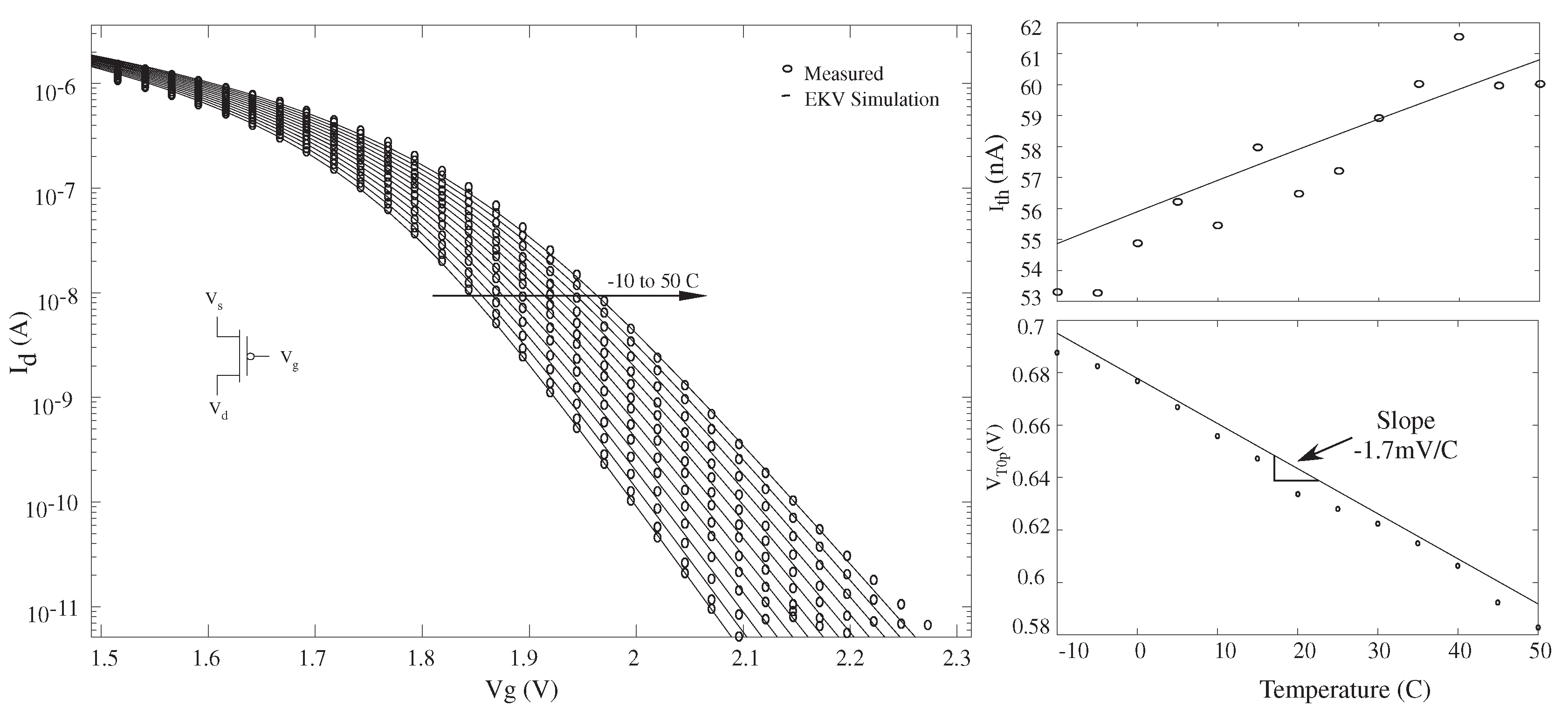
This model has been integrated as a part of the Scilab/Xcos environment [11]. Figure 3 shows measurement of pFET compiled on to the FPAA and simulation performed using the EKV model. The tool incorporates the above variation in , threshold voltage, and current at threshold voltage (). Figure 3 compares these variations between the simulated model and the measured results over a change of 60 °C. The measurements are silicon data obtained from the FPAA fabricated in 350 nm technology. Scaling of floating gates would follow similar trends as show in [17]. Simulation parameters have to adapted as the process scales to match the data from silicon.
Using the above model for simulation, similar measurements and simulations were performed for an nFET. The variation in threshold voltage and current at threshold voltage () for the devices are summarized in the Table 1. These parameters are extracted from the transfer characteristics using a EKV curve fit program in Scilab [18] with varying . The variations are shown as percentage changes in the parameters from its value at room temperature over 60 °C.
The consistency between the measurements and the model allows us to predict the first order behavior of circuits and systems compiled on the FPAA with temperature, thereby enabling temperature robust circuits and system design.
4. Temperature Dependence of Simple Single Ended Circuits
The models developed in the previous section predicts the behavior of circuits and systems on the FPAA. To illustrate, a common source amplifier, shown in the Figure 4, has a gain which is constant over temperature [19]. EKV model shown in Equation (1) could be reduced to following set of equations when :
Equating the channel current for nMOS and pMOS we have
In Equation (4), the offset is a manifestation of , threshold voltage difference between nFET () and pFET (), and . Figure 4 shows the transfer characteristics of a common source amplifier, measured on the FPAA and simulated using the models developed before, with pFET input. As seen in the Figure 4, the slope of the simulation and measurement remains relatively constant. The variation in the transition points of the transfer characteristics corresponding to different temperatures is associated with the offset () term that has dependence on and also due to the fact that the threshold voltage of pFET and an nFET vary differently over temperature.
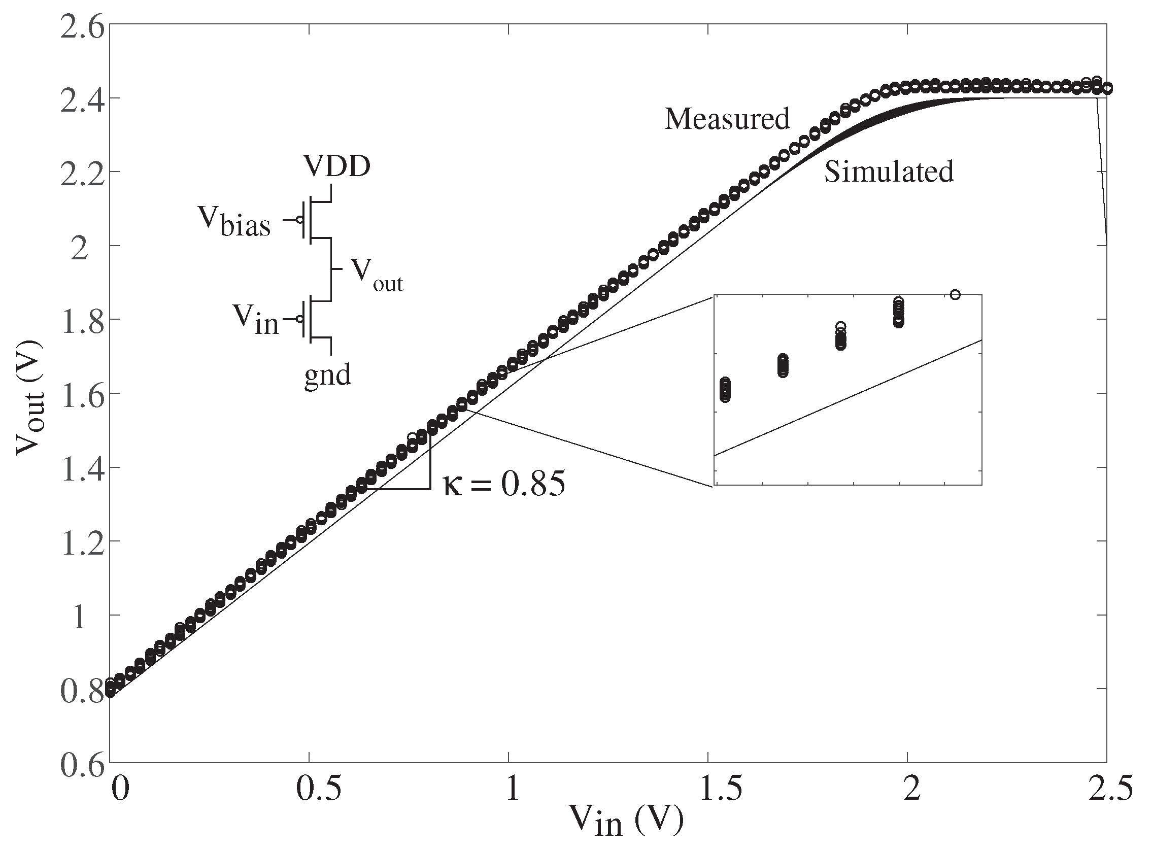
For temperature-robust transition points and gain, the circuit could be designed to utilize the same type of FET devices. The transfer characteristics of a two pFET-based common drain is given by Equation (5).
Thus the slope of the transfer characteristics is , since , which is invariant over temperature. Also, the term is independent of , threshold voltage, and and hence making the transition points invariant over temperature. Figure 5 shows the transfer characteristics of a common drain circuit with a pFET input. The measurement and simulation are plotted and have similar slope, that is, the kappa of the pFET input. The inset shows a zoom-in of the transfer characteristics measured over 60 °C.
5. Reducing Temperature Dependence in Programmable Circuits and System
Programming and biasing of FG switch or FG current source is generally done using a DAC. During programming mode, when the circuits and systems are getting compiled on the FPAA, the DAC allows for varying the bias of the gate for compensating the variation and mismatch on the FPAA [20]. It is assumed that temperature would not vary drastically while programming the device. In run mode however, when the implemented system is used for computation and processing on the FPAA, the temperature could vary based on the application, for example in wearable systems [3,4,12] or as a sensory node for analyzing speech [4]. A subthreshold current reference circuit, similar to a conventional current reference circuit [21], shown in the Figure 6 would bias the gate of a pFET which would reduce the temperature variation of the output current to 12.0%. The biasing current is constant and is not programmable unless of its transistor and the resistor values are changed. In the case of an FPAA, it would be possible to change by adding pFETs and nFETs in parallel. However, this would mean adding extra capacitance by the way of routing to different CABs.
5.1. FG-Based Reference Circuit in Subthreshold Region
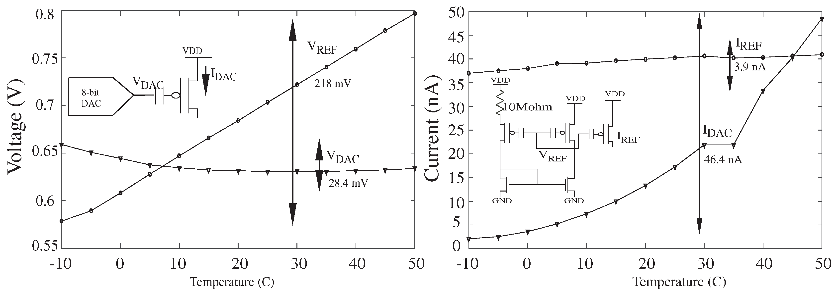
The reference circuit in Figure 7 is based on the bootstrap reference architecture [22]. However, unlike the conventional bootstrap reference architecture where the difference between the aspect ratios of pFETs is responsible for the reference generation, the in Figure 7 is generated because of the difference in the amount of charge stored at the floating-node of the FG pFETs. The bootstrap reference circuit in Figure 7 is compiled using FG pFET from the switch fabric, which are part of the local interconnect routing present in the CAB, and nFET current mirror, which is a part of the CAB elements described earlier.
Figure 7 also shows measurements of , , , and against temperature. A variation of 28.4 mV was observed in the DAC, thereby resulting in temperature variation of 189 ppm/°C with a linear range of 2.5 V. This manifests as large change in current, when used to bias a FG, since the voltage does not scale with temperature to compensate the variation in threshold voltage and . The bootstrap current reference has a variation of 218 mV in and the current mirror output has a temperature drift of 3.9 nA.
Evaluating the relationship of and over temperature of a current mirror built with a FG pFET, such as the one used in Figure 7 for biasing and shown in the Figure 8, is given by Equation (6).
if and in the above equation are equal then we have . In general, for a non FG current mirror there is a threshold voltage mismatch between the transistors that will lead to a variation of with temperature. The variation of current in this case could be modeled as
where is a reference temperature which could be room temperature for simplicity. This effect is important in case of a Vector Matrix Multiplication (VMM) , discussed in Section 6, where multiple FG pFETs are biased as a current mirror.
5.2. FG-Based Voltage Reference without Resistors
The main drawback of the reference circuits introduced in the previous section is the need for an external resistor for different biasing current. There are several resistorless bias reference circuits that take advantage of the availability of different or devices, i.e., high and low threshold devices [23,24]. The aforementioned techniques require an ASIC and availability of different threshold devices in the process.
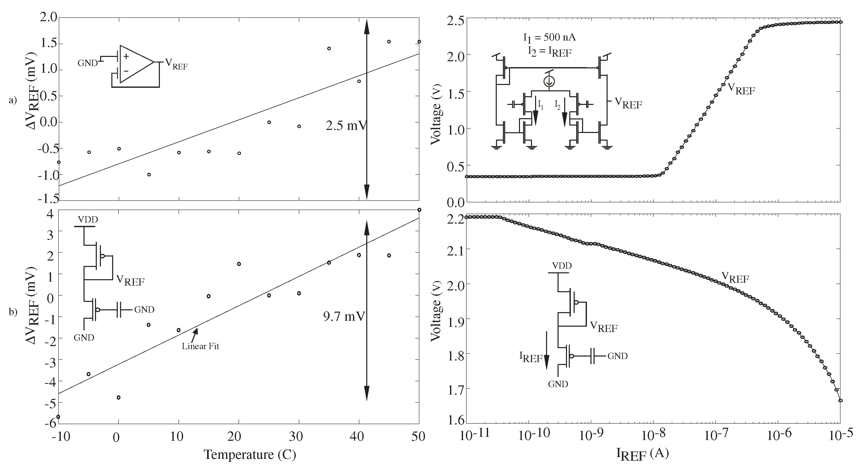
Here we propose to use FG to create a difference in threshold voltage by inducing charge at the floating node. This allows the bias of the reference with a different biasing value and to be able to directly compile the circuit onto the FPAA. Figure 9 shows the schematics of the proposed reference circuits. Figure 9a introduces a voltage reference circuit using a FGOTA. is generated by creating an offset between positive and negative terminals of the FGOTA. A of 2.5 mV, with respect to at 25 °C, was observed over a range of 60 °C. The range of voltage reference that could be generated with this reference is between 0.346 V to 2.44 V and is plotted in the Figure 9a. It should be noted that is constrained near the GND by the output buffer used for the measurement and is not due to the linear range of the FGOTA. Here, is the programming current and therefore an indicator of the charge programmed onto the FG, which is varied to tune the . For the measurements in Figure 9a, the FGOTA was biased at 2 A, and hence the power dissipated by the circuit is 5 W. This could change depending on the application, i.e., the load of the reference, and the power requirements. Considering the above linear range of the FGOTA based voltage reference, it has a temperature variation of 19.83 ppm/°C.
Figure 9b shows a voltage reference built using two devices. The FG transistor used in the circuit is part of the routing fabric in the FPAA whereas the pMOS transistor is part of the CAB. A variation of 9.7 mV over 60 °C was observed in case of this voltage reference with programming range of 1.66 V to 2.19 V. Considering this linear range, the reference has a temperature variability of 305 ppm/°C. The dependence of , in the case of Figure 9b, can be analyzed by reducing the EKV equation in Equation (1). As seen in Equation (8), has a weak dependence on and supply voltage VDD. In the following derivation, it is assumed that the of the FG pMOS and the diode connected pMOS is similar and that their .
It should be noted from the above equation that if the of two devices are equal, the output would be almost invariant over temperature. In addition, the above analysis holds only if the transistors, the FG transistor, and the pMOS are in the subthreshold saturation regime. Also, the two transistor circuit would have fairly significant power coupling as opposed to the FGOTA whose PSRR will be high.
6. Vector Matrix Multiplication (VMM)
A FG based Vector Matrix Multiplication (VMM) is one of the building blocks in an analog classifier [25,26]. It stores the weight of the classifier as a charge (Q) on the floating node of the FG pFET. The output of a VMM is a current signal, which is a product of input voltage and the weight stored on the floating node. The equation in Equation (1) can be modified as follows:
The above set of equations reveals the dependence of weight on temperature. Also, the would have a different relationship with the output with change in temperature given by . Thus the classifier, instead of having an output , will have a temperature dependent term.
To demonstrate the dependence of the VMM on temperature, when biased with a DAC, a (i.e., a 12 input and 1 output) VMM is compiled on the FPAA. As shown in Figure 10, a shift register is used to measure each FG output over 60 °C. A variation of 158 nA is observed when they are nominally biased around 50 nA at room temperature. This variation could lead to substantial errors while using the VMM in classification as temperature could vary depending on the application. As an example, when the classifier is used for classifying an acoustic signal from the knee joint [12], the system temperature is expected to change with the environment temperature (e.g., room temperature during activities performed at home or to hot/cold temperatures during outdoor activities). To address the issue, the current reference introduced in the Section 5.1 is used to bias the FG pMOS of the VMM. Figure 10 shows the variation of the VMM current when biased using the FG current reference. A maximum variation of 5.6 nA is observed in the current. This variation is due to the fact that there is a mismatch in the threshold voltage of the transistor resulting in , where is the gain factor from Equation (7).
The VMM weight is updated depending on the learning of the classifier and hence in practice the weight will have a certain compared to the biasing circuit. This will result in a gain , thereby leading to dependence of on temperature. If the output stage of the VMM is a Winner Take All (WTA) [27], which is the case in [3,12,25], the small variation would not affect the output of the classifier. This is due to the fact that a WTA compares relative current between the competing branches of VMM.
7. Variation of Band-Pass Filter
A based second order band-pass filter is used extensively for several signal processing systems [3,4,12]. A second order filter enables extracting frequency based features from the input signal with a low power consumption. Also, a FG based offers programmability over broad range of center frequencies by changing the bias of the FGOTAs. The input of the FGOTA is capacitively coupled to increase the linearity of the filter. The PSRR, CMRR, input referred noise, and other characteristics of the filter are described in detail here [28].
The inset in Figure 11 shows the schematic of a filter compiled in a single CAB of the FPAA. The FGOTA are biased using a FG pFET as seen in Figure 11. Figure 11 shows the frequency response of the band-pass filter over 60 °C of temperature change when biased using a DAC. Figure 11 also shows a variation in the center frequency, quality factor, and gain of the band-pass filter. The variation in center frequency is 2 KHz for a center frequency of 840 Hz at room temperature. This variation would lead to significant error in the processing and extraction of features in different signal processing systems.
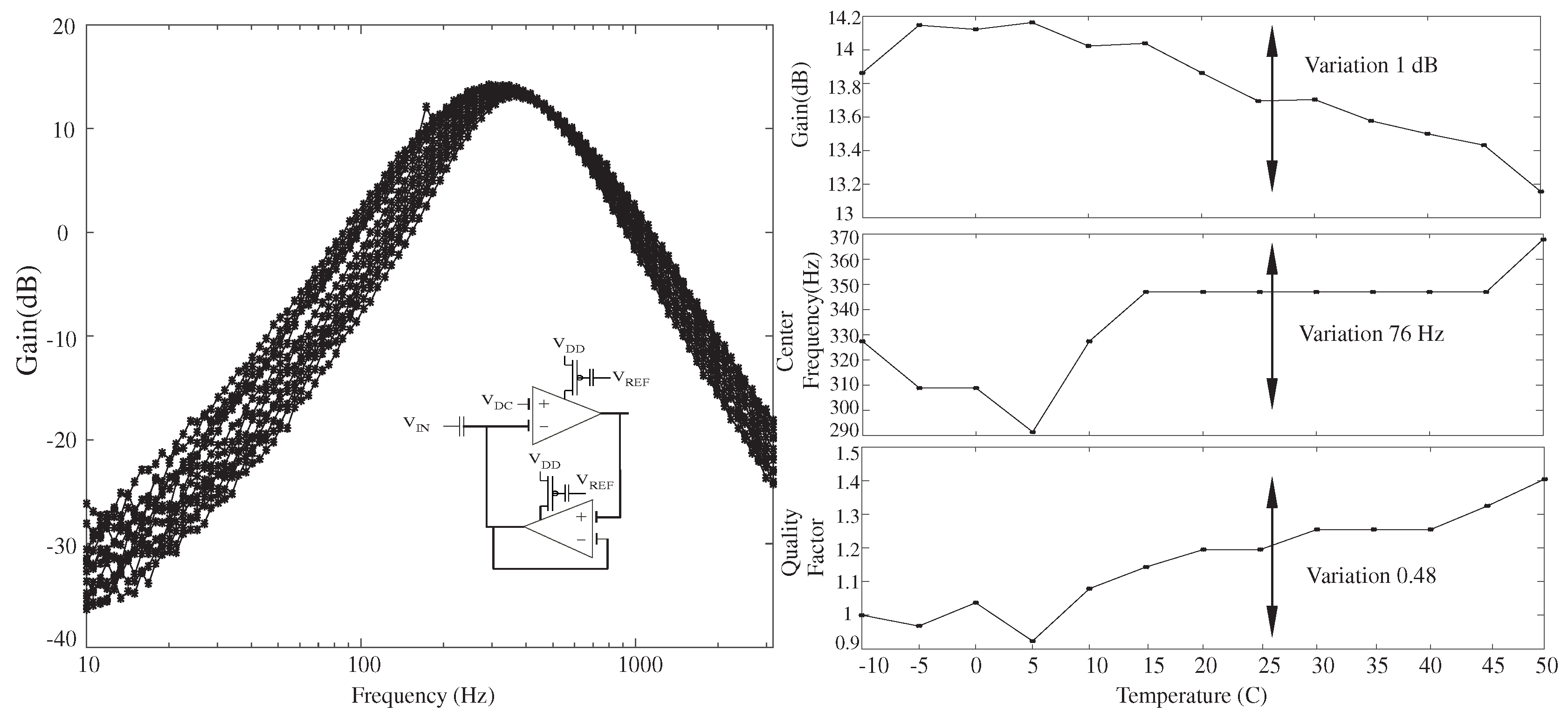
A FG based current reference generator introduced in the Section 5.1 would be suitable for biasing the filters. Figure 12 shows the bootstrap reference compiled along with the band pass filter. Figure 12 also shows the frequency response of the band-pass filter over a temperature variation of 60 °C. The Propotional To Absolute Temperature (PTAT) response of the FG based bootstrap reference helps in compensating the Complementary To Absolute Temperature (CTAT) variation in . Figure 12 also shows the variation in the characteristics of the bandpass filter namely quality factor (Q), center frequency (), and gain at the center frequency. As compared to the case where it was biased by a DAC, the variation in center frequency is reduced to 76 Hz, gain variation is 1 dB as opposed to 2 dB, and quality factor variation is 0.48 compared to 1.4. Measurements in the Figure 11 and Figure 12 were performed consecutively where the filter were biased first with a DAC and then with a FG current reference to keep other variations constant. The resulting temperature dependent variation of 76 Hz, observed in Figure 12, could be explained due to the fabrication related device-mismatch between the FG pMOS used in the reference circuit and the FG pMOS used as the biasing transistor of the FGOTAs in the bandpass filter. In addition, there are design-related mismatches in the aforementioned FG pMOS devices as well. For instance, the coupling capacitor of the FG pMOS in the reference circuit is 8 fF as opposed to 43 fF incase of the FGOTA biasing device. The other source of mismatch is also due to different of the FG pMOS transistors, which is in the case of the FG reference circuit and . In subsequent designs of the FPAA, these variations will be reduced by keeping a single size of FG transistors for all the devices on the SoC.
8. Summary and Discussion
There has been a growing interest in using FPAA for rapid prototyping of mixed signal systems, performing mixed and analog signal processing for wide ranging applications, and using programmability and reconfigurability to increase system performance and energy efficiency [5,29,30,31]. Hence, it becomes more important to study the effects of temperature on a reconfigurable platform and investigate methods that could reduce these variations. A FG temperature compensation structure as part of the CAB is used to reduce the variation in current over temperature [32]. This work presents several circuits, models, and techniques to estimate and reduce the temperature variation of such a system.
The simulation performed using the model developed based on the EKV models were in close agreement with the measured data. These models created for simple nFET and pFET devices were then used to study the temperature behavior of simple single ended circuits and were compared with measurement results. The intuition created here led to building and designing several of the current and voltage references introduced in subsequent sections. The references developed in this work are a part of the Scilab/Xcos environment as a block thereby enabling easy compilation as part of a larger system.
A bootstrap current reference is introduced to bias FG devices on the FPAA. The performance of the bootstrap reference is studied over temperature and the measured results from the FPAA are presented. The FG reference circuit is also used to bias two critical components of analog signal processing chain, namely the VMM and the second order bandpass filer. Their performance over temperature when biased using a DAC and the FG reference circuit is studied. A variation of 156 nA was observed in the output current of the VMM when biased with a DAC as opposed to a variation of 5.6 nA, when biased with FG current reference circuit. The bandpass filter’s center frequency varies by 2 KHz when biased with a DAC whereas in case of FG reference circuit it varies by 76 Hz.
The work also presents two resistorless voltage references with wide range of programmable voltages. The FGOTA based voltage reference has a temperature variability of 19.83 ppm/°C whereas the two transistor based voltage reference achieves a precision of 305 ppm/°C. FGOTA could also be used as an error amplifier in an LDO without having to generate a separate reference voltage [33]. All measurements were performed on the FPAA, which is powered using a microUSB. PSRR measurements were not performed since body of all pFET devices are connected to the fixed microUSB supply, thus preventing accurate PSRR measurements.
FG devices would requires a programming infrastructure, an overhead in terms of area and power, and would be infeasible as a stand-alone structure. However, in case of an FPAA there are more then half a million FG devices and thus would make it feasible to have a single programming infrastructure. Additionally, using FG devices as routing switches allows for a lower power consumption compared to an FPGA where dedicated SRAM is required to store the design.
Author Contributions
Sahil Shah, Hakan Toreyin and Jennifer Hasler conceived and designed the experiments; Sahil Shah performed the experiments; Sahil Shah and Jennifer Hasler analyzed the data; Sahil Shah and Aishwarya Natarajan developed the transistor models to predict the behaviour of the device over temperature; Sahil Shah and Hakan Toreyin wrote the paper.
Conflicts of Interest
The authors declare no conflict of interest.
References
- Hersek, S.; Toreyin, H.; Inan, O.T. A Robust System for Longitudinal Knee Joint Edema and Blood Flow Assessment Based on Vector Bioimpedance Measurements. IEEE Trans. Biomed. Circuits Syst. 2016, 10, 545–555. [Google Scholar]
- Toreyin, H.; Shah, S.; Hersek, S.; Inan, O.T.; Hasler, J. Proof-of-Concept Energy-Efficient and Real-Time Hemodynamic Feature Extraction from Bioimpedance Signals using a Mixed-Signal Field Programmable Analog Array. In Proceedings of the International Conference on Biomedical and Health Informatics (BHI), Orlando, FL, USA, 16–19 Feburary 2017. [Google Scholar]
- Shah, S.; Toreyin, H.; Inan, O.T.; Hasler, J. Reconfigurable Analog Classifier For Knee-Joint Rehabilitation. IEEE Eng. Med. Biol. Soci. 2016. [Google Scholar] [CrossRef]
- Sahil, S.; Jennifer, H. Low Power Speech Detector On A FPAA. Presented at ISCAS 2017, Baltimore, MD, USA, 28–31 May 2017. [Google Scholar]
- George, S.; Kim, S.; Shah, S.; Hasler, J.; Collins, M.; Adil, F.; Wunderlich, R.; Nease, S.; Ramakrishnan, S. A Programmable and Configurable Mixed-Mode FPAA SoC. IEEE Trans. Very Large Scale Integr. (VLSI) Syst. 2016, 24, 2253–2261. [Google Scholar] [CrossRef]
- Teague, C.; Hersek, S.; Toreyin, H.; Millard-Stafford, M.L.; Jones, M.L.; Kogler, G.F.; Sawka, M.N.; Inan, O.T. Novel approaches to measure acoustic emissions as biomarkers for joint health assessment. In Proceedings of the 2015 IEEE 12th International Conference on Wearable and Implantable Body Sensor Networks (BSN), Cambridge, MA, USA, 9–12 June 2015; pp. 1–6. [Google Scholar]
- Etemadi, M.; Inan, O.T.; Heller, J.A.; Hersek, S.; Klein, L.; Roy, S. A Wearable Patch to Enable Long-Term Monitoring of Environmental, Activity and Hemodynamics Variables. IEEE Trans. Biomed. Circuits Syst. 2016, 10, 280–288. [Google Scholar] [CrossRef] [PubMed]
- Shah, S.; Smith, J.; Stowell, J.; Christen, J.B. Biosensing platform on a flexible substrate. Sens. Actuators B Chem. 2015, 210, 197–203. [Google Scholar] [CrossRef]
- Ahuja, B.K.; Vu, H.; Laber, C.A.; Owen, W.H. A very high precision 500-nA CMOS floating-gate analog voltage reference. IEEE J. Solid-State Circuits 2005, 40, 2364–2372. [Google Scholar] [CrossRef]
- Kim, S.; Shah, S.; Wunderlich, R.; George, S.; Hasler, J. CAD Synthesis Tools for Large-Scale Floating-Gate FPAA System. Trans. Comput. Aided Des. 2017. under review. [Google Scholar]
- Natarajan, A.; Hasler, J. Modeling, simulation and implementation of circuit elements in an open-source tool set on the FPAA. Anal. Integr. Circuits Signal Process. 2017, 91, 119–130. [Google Scholar] [CrossRef]
- Shah, S.; Teague, C.N.; Inan, O.T.; Hasler, J. A Proof-of-Concept Classifier for Acoustic Signals from the Knee Joint on a FPAA. In Proceedings of the 2016 IEEE SENSORS, Orlando, FL, USA, 30 Octorber–3 November 2016. [Google Scholar]
- Gurun, G.; Tekes, C.; Zahorian, J.; Xu, T.; Satir, S.; Karaman, M.; Hasler, J.; Degertekin, F.L. Single-chip CMUT-on-CMOS front-end system for real-time volumetric IVUS and ICE imaging. IEEE Trans. Ultrason. Ferroelectr. Freq. Control 2014, 61, 239–250. [Google Scholar] [CrossRef] [PubMed]
- Kim, S.; Hasler, J.; George, S. Integrated Floating-Gate Programming Environment for System-Level ICs. IEEE Trans. Very Large Scale Integr. (VLSI) Syst. 2016, 24, 2242–2252. [Google Scholar] [CrossRef]
- Enz, C.C.; Krummenacher, F.; Vittoz, E.A. An analytical MOS transistor model valid in all regions of operation and dedicated to low-voltage and low-current applications. Anal. Integr. Circuits Signal Process. 1995, 8, 83–114. [Google Scholar] [CrossRef]
- Pierret, R. Semiconductor Device Fundamentals; Addison-Wesley: Boston, MA, USA, 1996. [Google Scholar]
- Hasler, J.; Kim, S.; Adil, F. Scaling Floating-Gate Devices Predicting Behavior for Programmable and Configurable Circuits and Systems. J. Low Power Electron. Appl. 2016, 6, 13. [Google Scholar] [CrossRef]
- Minch, B. EKV MOS Transistor Model Summary. Available online: http://madvlsi.olin.edu/circuits/handouts.html (accessed on 2 Feburary 2017).
- Degnan, B.P. Temperature Robust Programmable Subthreshold Circuits Through A Balanced Force Approach. Ph.D. Thesis, Georgia Institute of Technology, Atlanta, GA, USA, 2013. [Google Scholar]
- Kim, S.; Shah, S.; Hasler, J. Calibration of Floating-Gate SoC FPAA System. IEEE Trans. Very Large Scale Integr. (VLSI) Syst. 2017, 25, 2649–2657. [Google Scholar] [CrossRef]
- Vittoz, E.; Fellrath, J. CMOS analog integrated circuits based on weak inversion operations. IEEE J. Solid-State Circuits 1977, 12, 224–231. [Google Scholar] [CrossRef]
- Srinivasan, V.; Serrano, G.; Twigg, C.M.; Hasler, P. A Floating-Gate-Based Programmable CMOS Reference. IEEE Trans. Circuits Syst. I Regul. Pap. 2008, 55, 3448–3456. [Google Scholar] [CrossRef]
- Georgiou, J.; Toumazou, C. A resistorless low current reference circuit for implantable devices. In Proceedings of the 2002 IEEE International Symposium on Circuits and Systems (Cat. No. 02CH37353), Phoenix-Scottsdale, AZ, USA, 26–29 May 2002; Volume 3, pp. III-193–III-196. [Google Scholar]
- Seok, M.; Kim, G.; Blaauw, D.; Sylvester, D. A Portable 2-Transistor Picowatt Temperature-Compensated Voltage Reference Operating at 0.5 V. IEEE J. Solid-State Circuits 2012, 47, 2534–2545. [Google Scholar] [CrossRef]
- Ramakrishnan, S.; Hasler, J. Vector-Matrix Multiply and Winner-Take-All as an Analog Classifier. IEEE Trans. Very Large Scale Integr. (VLSI) Syst. 2014, 22, 353–361. [Google Scholar] [CrossRef]
- Ramakrishnan, S.; Basu, A.; Chiu, L.K.; Hasler, J.; Anderson, D.; Brink, S. Speech Processing on a Reconfigurable Analog Platform. IEEE Trans. Very Large Scale Integr. (VLSI) Syst. 2014, 22, 430–433. [Google Scholar] [CrossRef]
- Lazzaro, J.; Ryckebusch, S.; Mahowald, M.; Mead, C.A. Winner-Take-All Networks of O(N) Complexity. In Advances in Neural Information Processing Systems 1; Touretzky, D., Ed.; Morgan-Kaufmann: Burlington, MA, USA, 1989; pp. 703–711. [Google Scholar]
- Graham, D.W.; Hasler, P.E.; Chawla, R.; Smith, P.D. A Low-Power Programmable Bandpass Filter Section for Higher Order Filter Applications. IEEE Trans. Circuits Syst. I Regul. Pap. 2007, 54, 1165–1176. [Google Scholar] [CrossRef]
- Guo, N.; Huang, Y.; Mai, T.; Patil, S.; Cao, C.; Seok, M.; Sethumadhavan, S.; Tsividis, Y. Energy-Efficient Hybrid Analog/Digital Approximate Computation in Continuous Time. IEEE J. Solid-State Circuits 2016, 51, 1514–1524. [Google Scholar] [CrossRef]
- Dorigo, D.D.; Manoli, Y. An OTA-C signal processing FPAA with 305 MHz GBW and integrated frequency-independent filter tuning. In Proceedings of the 2016 IEEE Asian Solid-State Circuits Conference (A-SSCC), Toyama, Japan, 7–9 November 2016; pp. 61–64. [Google Scholar]
- Becker, J.; Anders, J.; Ortmanns, M. A continuous-time field programmable analog array with 1 GHz GBW. In Proceedings of the 2016 IEEE International Conference on Electronics, Circuits and Systems (ICECS), Monte Carlo, Monaco, 11–14 December 2016; pp. 209–212. [Google Scholar]
- Dilello, A.; Andryzcik, S.; Kelly, B.M.; Rumberg, B.; Graham, D.W. Temperature Compensation of Floating-Gate Transistors in Field-Programmable Analog Arrays. In Proceedings of the IEEE Internation Symposium on Circuits and System, Baltimore, MD, USA, 28 May 2017. [Google Scholar]
- Peng, S.Y.; Liu, L.H.; Chang, P.K.; Wang, T.Y.; Li, H.Y. A Power-Efficient Reconfigurable Output-Capacitor-Less Low-Drop-Out Regulator for Low-Power Analog Sensing Front-End. IEEE Trans. Circuits Syst. I Regul. Pap. 2017, 64, 1318–1327. [Google Scholar]
Figure 1.
Proposed method to reduce temperature variability while compiling a system for a desired application on a FPAA. The tool infrastructure offers flexibility depending on the user. A system designer would choose from multiple voltage and current references depending on the application [3,4,12,13]. Then, the system along with the selected references would be compiled on the FPAA. This would enable wide range of programmable and reconfigurable temperature robust systems. In case of a circuit designer the FPAA tool infrastructure enables designing a custom reference circuit. The circuit could be simulated, with models based on EKV, before compiling the design on the hardware.
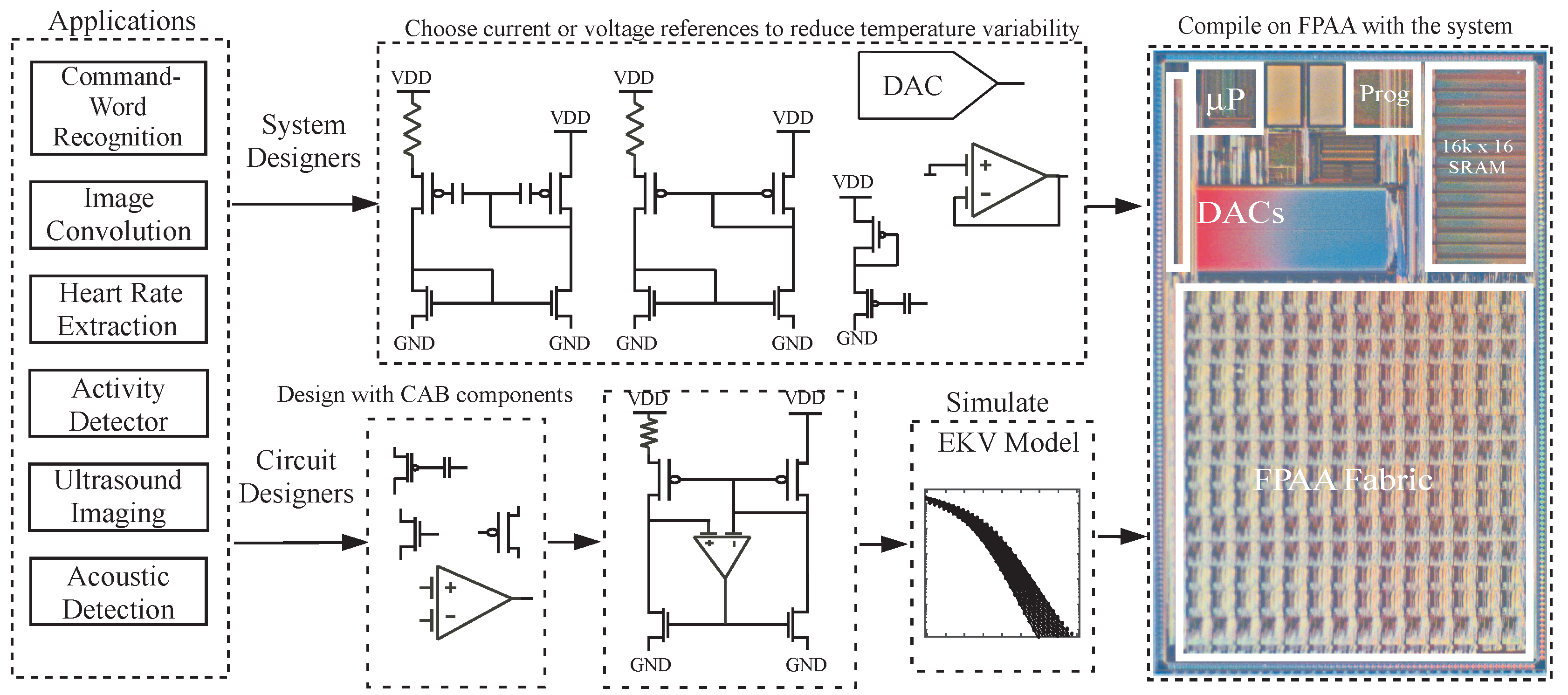
Figure 2.
FPAA structure with its components. FPAA fabric is made of computational analog block (A) and computational logic block (D). A part of the FPAA computational analog block (CAB) along with its elements. The switch fabric of the FPAA is made of Floating Gate (FG) elements. Also, the biasing of Operational Transconductance Amplifier (OTA) is done using a FG pFET transistor. The gate of these FG pFET transistor could be biased using a 7-bit DAC or a bootstrap voltage reference.
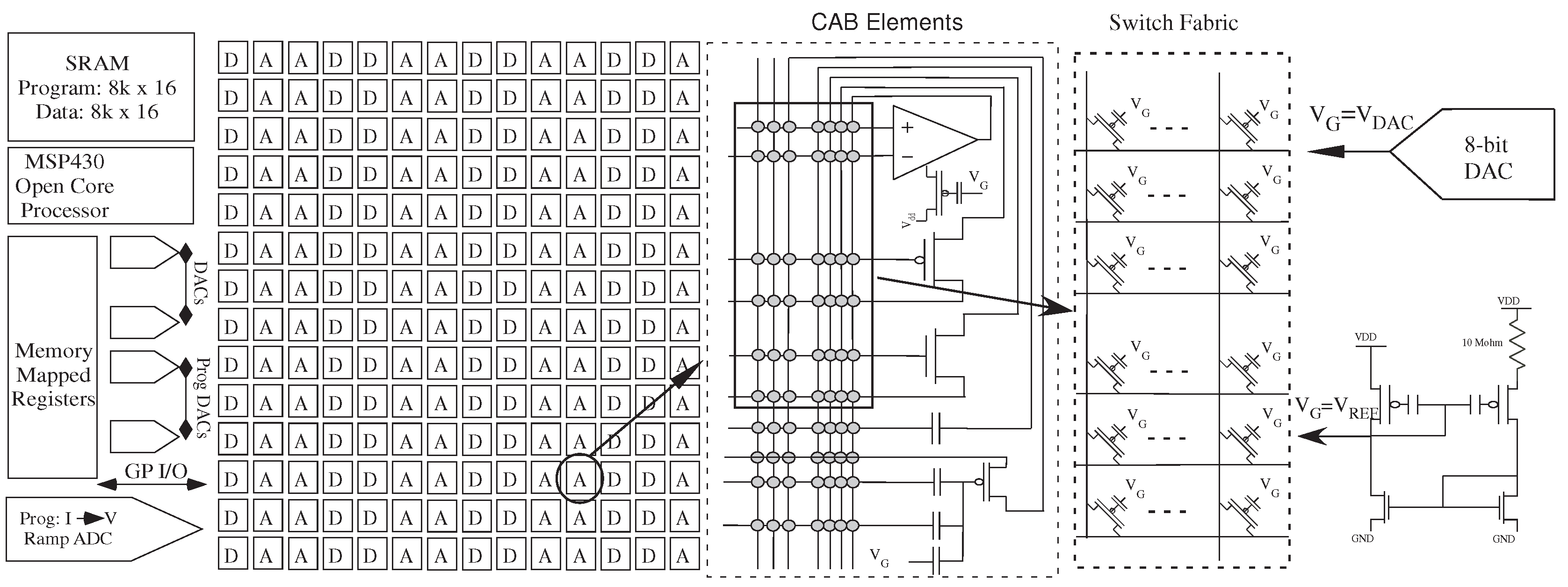
Figure 3.
vs transfer characteristics of PMOS over Temperature. EKV modeling is used for modeling the transfer characteristics of a PMOS. , current at threshold voltage, and threshold voltage are also plotted over temperature. The simulated values are consistent with the measured values. The and threshold voltages are extracted by curve fitting onto to the output current in both measurement and simulation to be consistent.

Figure 4.
Transfer function of a common source amplifier, measured and simulated using the models developed in the previous section, with temperature. The slope, and hence the gain of the common source amplifier, is also plotted. Slope is constant with temperature. The transition of with for different temperature is also shown. The transition changes over temperature because the threshold voltage of nMOS and pMOS varies differently.
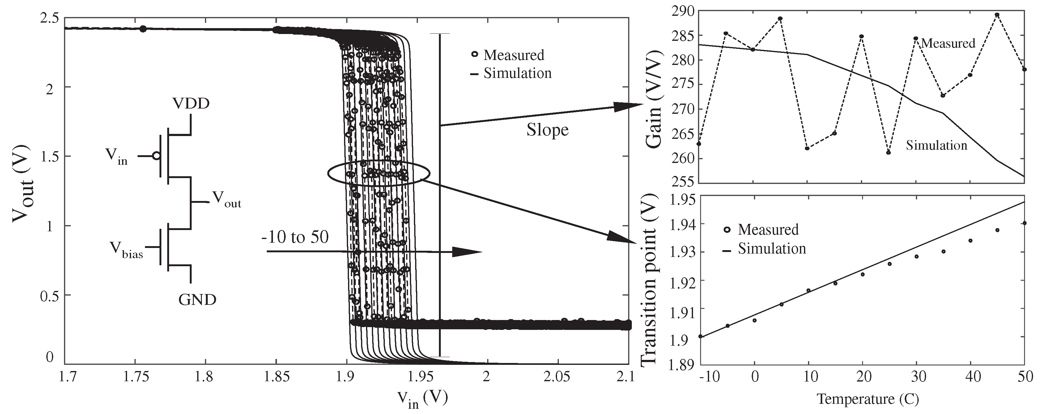
Figure 5.
Transfer function of a common drain amplifier, measured and simulated using the models developed in the previous section, with temperature. The slope and the transition offset of the circuit is constant with temperature because the variation in threshold voltage of the two pMOS devices are similar. A slope of 0.85, which is the of the pMOS device, is measured from the circuit compiled on the FPAA.

Figure 6.
A bias reference circuit compiled on to the FPAA. The circuit has to use multiple pFET transistors to create the required multiplication. This is the major drawback since it has to use multiple CABs.
Figure 6.
A bias reference circuit compiled on to the FPAA. The circuit has to use multiple pFET transistors to create the required multiplication. This is the major drawback since it has to use multiple CABs.
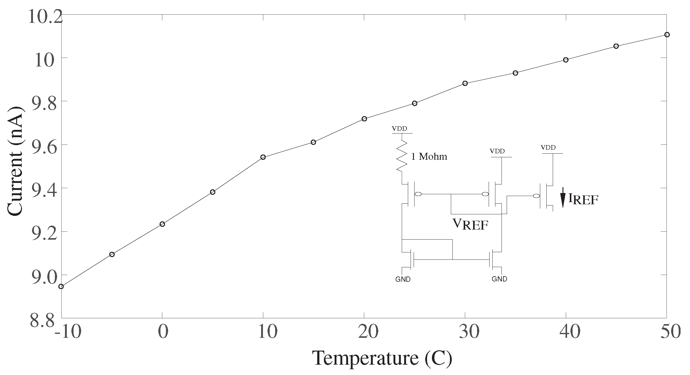
Figure 7.
A FG based bootstrap reference circuit compiled on the FPAA for biasing the FG transistors. The DAC which is generally used to bias the FG transistor is also characterized over temperature. Output of the reference generator () is plotted over a temperature variation of 60 °C. The output of the DAC is also measured over the same temperature range. Also, the effects of temperature on the drain current is studied by biasing a FG transistor in both modes, i.e., bias using a DAC and the bootstrap reference circuit.

Figure 8.
A simple FG pFET based current mirror. The mismatch between the two transistor causes to be not equal to . This also results in temperature dependence of assuming is kept constant.
Figure 8.
A simple FG pFET based current mirror. The mismatch between the two transistor causes to be not equal to . This also results in temperature dependence of assuming is kept constant.
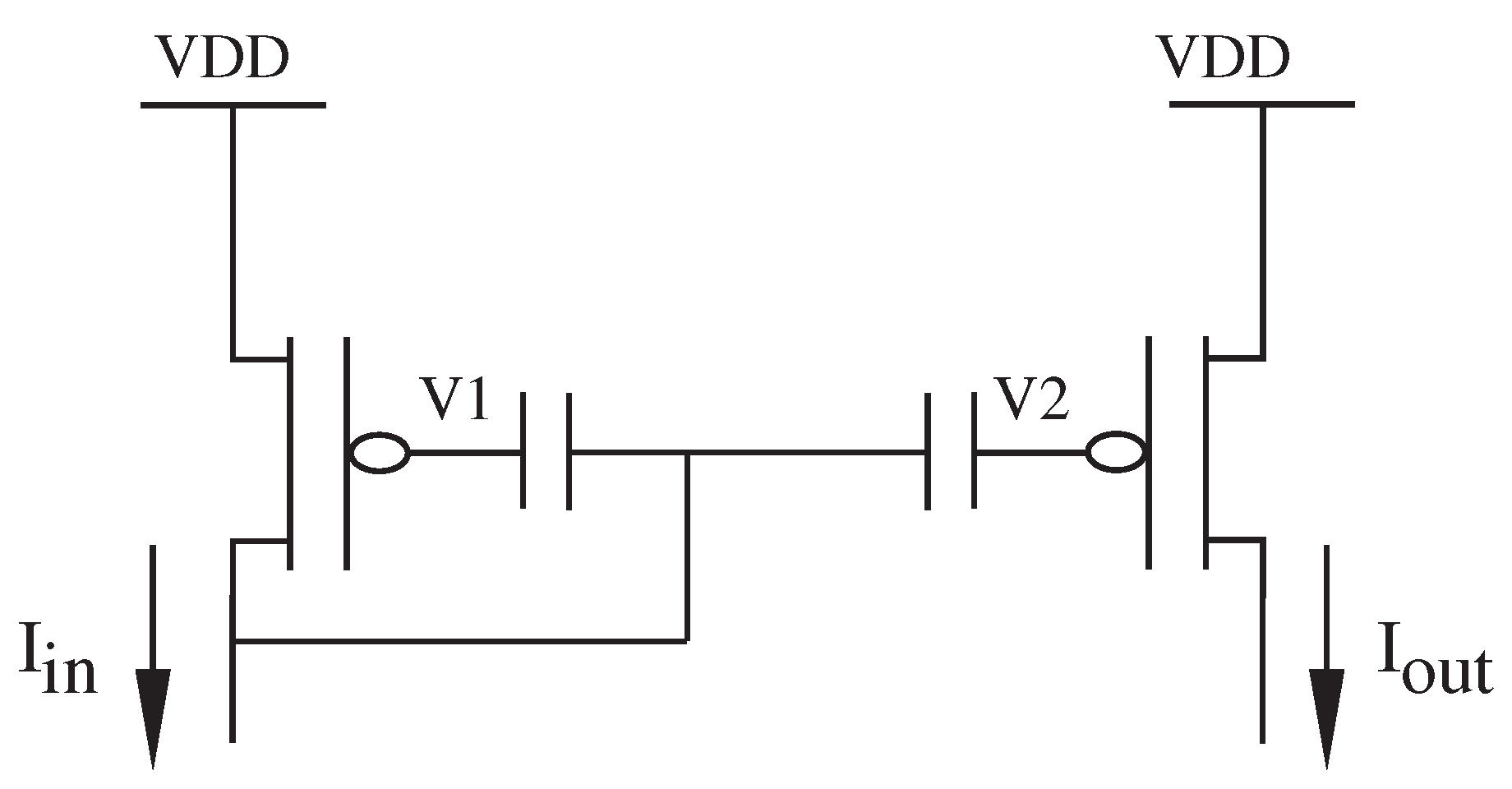
Figure 9.
Programmable voltage reference without resistors. (a) The figure on the top shows results from a voltage reference designed using FGOTA connected in a follower configuration. is generated by creating an offset between the positive and negative terminals of the FGOTA. A variation of 2.5 mV was observed in the reference voltage value over a change of 60 °C. The reference has a programmable range of 0.346 V to 2.441 V and this is shown in the second part of the figure; (b) A programmable voltage reference designed using a diode connected pFET and a FG pFET from the routing infrastructure. A variation of 9.7 mV was observed for a change of 60 °C. The range of this reference is 1.66 V to 2.19 V.

Figure 10.
A typical implementation of a Vector Matrix Multiplication, shown here with a shift register for measurement, in a FG-based FPAA. The two measurements corresponds to two different experimental setups. one where a DAC is used to bias the FG whereas the other corresponds to a FG biased using the voltage reference discussed earlier. A current variation of 158 nA was observed over 60 °C when the VMM, programmed to get 50 nA at room temperature, was biased using a DAC. A variation of 5.6 nA was observed in case of the VMM biased using the voltage reference.
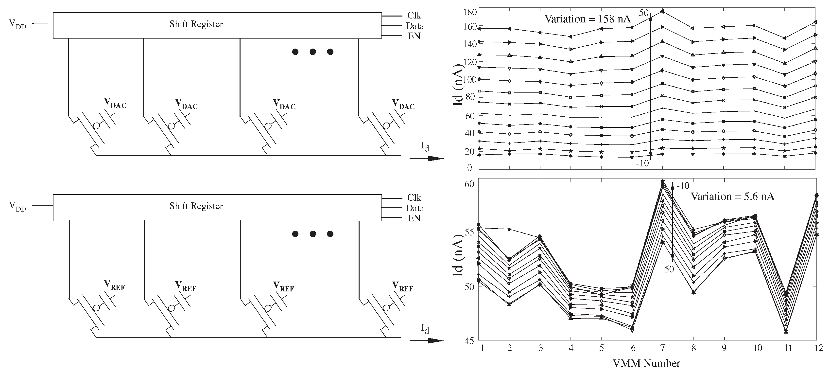
Figure 11.
Measured frequency response of second order band-pass filter over temperature. A FG pFET is used as a biasing transistor for the OTA. Here, the gate of FG pFET is biased using a DAC as seen in the inset of the frequency response graph. A variation of 2 Khz was observed in center frequency of the filter. A variation of 2 dB in gain and 1.4 in the quality factor of the filter was observed.
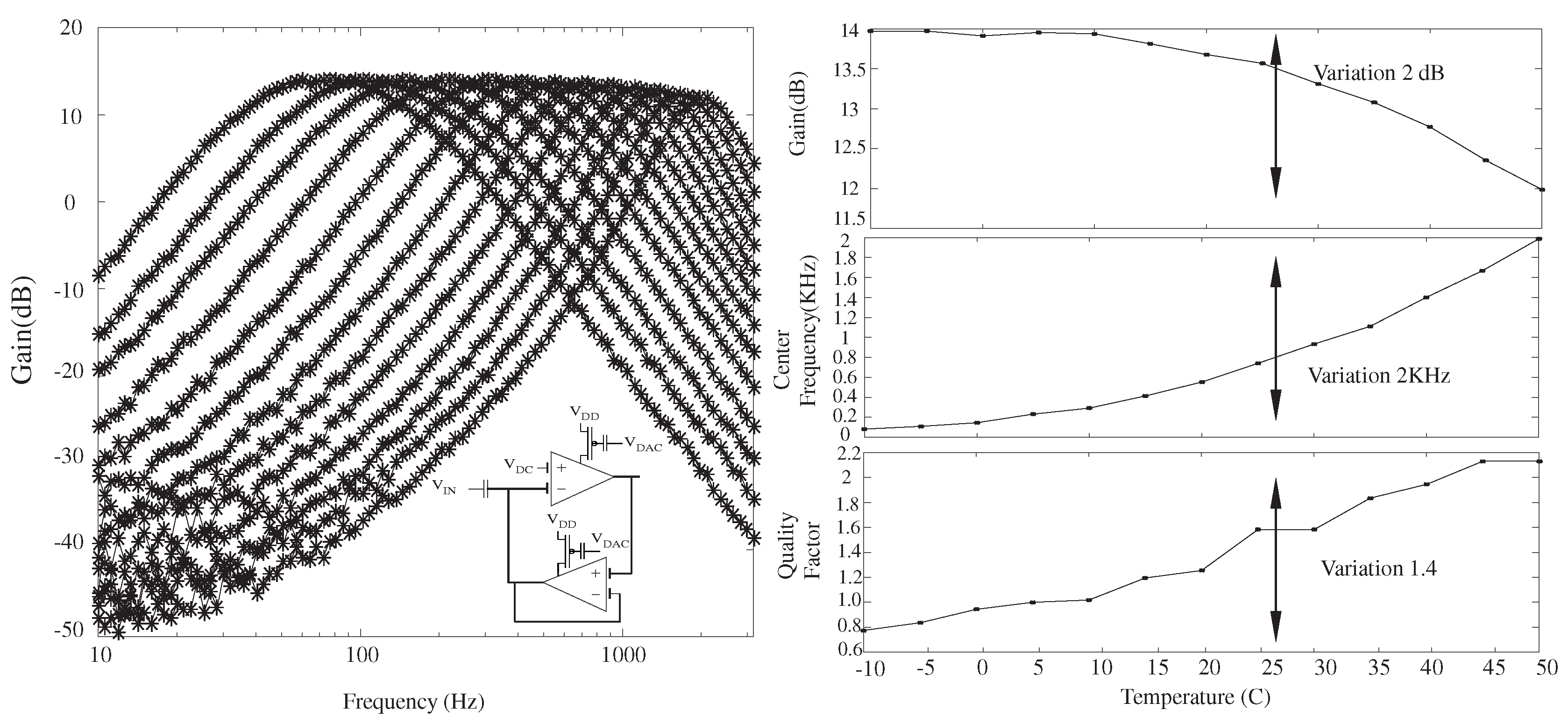
Figure 12.
Measured frequency response of second order band-pass filter over temperature. Here, the gate of the FG pFET is biased using the FG based voltage reference. A variation of 76 Hz was observed in case of the center frequency. A variation of 0.48 in quality factor and 1 dB in gain, at the center frequency, of the filter was observed.

Table 1.
Comparison of simulated and measured data: Percentage change over 60 °C.
| Device Parameter | Measured | Simulated | ||||||
|---|---|---|---|---|---|---|---|---|
| Threshold Voltage | Threshold Voltage | |||||||
| pFET | −0.28% | −1.7 mV/C | 0.2% | 2000 ppm/C | −0.27% | −1.7 mV/C | 0.17% | 1700 ppm/C |
| nFET | −0.26% | −1.1 mV/C | 0.24% | 2400 ppm/C | −0.22% | −0.95 mV/C | 0.17% | 1700 ppm/C |
© 2017 by the authors. Licensee MDPI, Basel, Switzerland. This article is an open access article distributed under the terms and conditions of the Creative Commons Attribution (CC BY) license (http://creativecommons.org/licenses/by/4.0/).
Share and Cite
MDPI and ACS Style
Shah, S.; Toreyin, H.; Hasler, J.; Natarajan, A. Models and Techniques for Temperature Robust Systems on a Reconfigurable Platform. J. Low Power Electron. Appl. 2017, 7, 21. https://doi.org/10.3390/jlpea7030021
AMA Style
Shah S, Toreyin H, Hasler J, Natarajan A. Models and Techniques for Temperature Robust Systems on a Reconfigurable Platform. Journal of Low Power Electronics and Applications. 2017; 7(3):21. https://doi.org/10.3390/jlpea7030021
Chicago/Turabian StyleShah, Sahil, Hakan Toreyin, Jennifer Hasler, and Aishwarya Natarajan. 2017. "Models and Techniques for Temperature Robust Systems on a Reconfigurable Platform" Journal of Low Power Electronics and Applications 7, no. 3: 21. https://doi.org/10.3390/jlpea7030021
Note that from the first issue of 2016, this journal uses article numbers instead of page numbers. See further details here.