Article

Inkjet Printed Fully-Passive Body-Worn Wireless Sensors for Smart and Connected Community (SCC)

1
Electrical and Computer Engineering, Herff College of Engineering, University of Memphis, Memphis, TN 38152, USA
2
Division of Social and Behavioral Sciences, School of Public Health, University of Memphis, Memphis, TN 38152, USA
3
Henderson County Community Hospital, Lexington, TN 38351, USA
4
Baptist Minor Medical Center, Memphis, TN 38111, USA
*
Author to whom correspondence should be addressed.
J. Low Power Electron. Appl. 2017, 7(4), 26; https://doi.org/10.3390/jlpea7040026
Submission received: 30 September 2017 / Revised: 30 October 2017 / Accepted: 4 November 2017 / Published: 9 November 2017
(This article belongs to the Special Issue Low-Power Electronic Circuits for Monolithic Smart Wireless Sensors)

Abstract

:
Future Smart and Connected Communities (SCC) will utilize distributed sensors and embedded computing to seamlessly generate meaningful data that can assist individuals, communities, and society with interlocking physical, social, behavioral, economic, and infrastructural interaction. SCC will require newer technologies for seamless and unobtrusive sensing and computation in natural settings. This work presents a new technology for health monitoring with low-cost body-worn disposable fully passive electronic sensors, along with a scanner, smartphone app, and web-server for a complete smart sensor system framework. The novel wireless resistive analog passive (WRAP) sensors are printed using an inkjet printing (IJP) technique on paper with silver inks (Novacentrix Ag B40, sheet resistance of 21 mΩ/sq) and incorporate a few discrete surface mounted electronic components (overall thickness of <1 mm). These zero-power flexible sensors are powered through a wireless inductive link from a low-power scanner (500 mW during scanning burst of 100 ms) by amplitude modulation at the carrier signal of 13.56 MHz. While development of various WRAP sensors is ongoing, this paper describes development of a WRAP temperature sensor in detail as an illustration. The prototypes were functionally verified at various temperatures with energy consumption of as low as 50 mJ per scan. The data is analyzed with a smartphone app that computes severity (Events-of-Interest, or EoI) using a real-time algorithm. The severity can then be anonymously shared with a custom web-server, and visualized either in temporal or spatial domains. This research aims to reduce ER visits of patients by enabling self-monitoring, thereby improving community health for SSC.

Graphical Abstract

1. Introduction

New generation of smart and connected technologies have fundamentally and positively influenced individual’s perspectives, behaviors, and interactions. Such transformational technology is expected to provide significant benefits to communities with interlocking physical, social, behavioral, economic, and infrastructural challenges. Smart and Connected Communities (SCC) will utilize distributed sensors and embedded computing to seamlessly generate meaningful interpretations to benefit individuals, the community, and society.
Mobile Health (mHealth) technology has enabled a revolution in computerized health interventions through mobile (smart) phones, with an estimated 200 million smartphone users in the USA with an estimated 75% of Americans and 68% of adults worldwide own cell phones, which can potentially be utilized to expand mHealth initiatives [1]. One study revealed that one in six Americans already owns a piece of wearable technology [2]. Current smartphones have some integrated sensors, e.g., Inertial Measurement Unit (IMU), cameras, light sensors, Radio Frequency Identification (RFID), Near Field Communication (NFC) interfaces, and Global Positioning Systems (GPS). Furthermore, many wearables (e.g., smart watches) include proximity sensor, heart rate sensor, and pulse oximetry. However, these sensors are unable to collect clinically important physiological signals, such as core-body temperature, Electrocardiography (ECG/EKG), and respiration rate. This leads to a small modality of physiological signal monitoring with smartphones and is a severe limiting factor for mHealth technology. One study found that 25% of users of wearable devices do not sustain usage after the first 5 months, and the utilization rate reduces to less than 40% within 2 years [2]. A major burden is lifestyle compatibility [3], indicating that a simplified wearing experience (such as eliminating batteries) may yield better results.
Even though high energy density miniature batteries, newer energy harvesting techniques, and contactless remote sensing are promising [4,5,6,7], fully passive wirelessly powered sensors present a significant opportunity. Such technology allows for the collection of physiological data that requires body contact, such as core-body temperature and ECG. They are also low-maintenance and low-cost [8,9]. Traditional fully passive wireless sensors are based on digital data encoding and require an Application Specific Integrated Circuit (ASIC) chip on the sensor [10,11,12]. This chip powers up using wireless energy to collect data from the sensor, e.g., RFID tag [13,14,15]. A scanner (commonly referred to as a reader) transmits wireless carrier signal to the passive sensor (e.g., RFID tag) [10,12]. The chip receives the wireless power, turns on the electronic circuitry, and wirelessly retransmits the ID/data to the scanner. The operating principle can be either inductive loading or backscattering for near-field (sub-100 MHz) or far-field region (over 100 MHz, e.g., UHF), respectively [12,16]. Wireless power from the reader must exceed the “turn-on power” to activate the chip (between 10 μW and 1 mW), while the maximum reading speed is typically 0.5 s [12,17]. For signals that require a high sampling rate, such as ECG and HRV signals, the solution is to keep the chip continuously powered [18,19,20,21,22,23,24,25,26] through a wireless power transfer technique that consumes higher energy compared to chip-less counterparts.
While digital fully passive wireless sensors seem attractive, there is another possibility of fully passive wireless sensors that are “chip-less”. These sensors are able to achieve up to five orders of power saving and up to a 100 ksps data rate at a lower cost (since an ASIC chip is not required). In this chip-less approach, data are transmitted in analog format [15,16,27]. There are two options for analog data encoding; frequency shifting using a capacitor and amplitude shifting using resistor. The capacitive approach can be realized using varactor or diodes that respond to bioelectric (voltage) signals. Towe et al. [27,28,29,30], Chae et al. [30,31,32], and Lekkala et al. [33] are among the pioneers to develop such capacitive wireless passive sensors. A surface acoustic wave (SAW) chip can also be used as a delay line for the modulated signals, thus differentiating backscattered signal from the interrogating signal [34,35,36]. A major drawback of capacitive sensing is that the sensed signal is limited to voltage only. In contrast, we have developed fully-passive wireless sensors based on a resistive approach, “Wireless Resistive Analog Passiv” (WRAP) sensors, that can sense bioelectric potential (voltage signal) as well as other physical stimuli (e.g., pressure, temperature, light) [37,38,39]. The advantages of WRAP sensors are low cost, high sampling rate, low power, and the possibility of prototyping on flexible substrates using inkjet printing (IJP) technique as discussed below.
Traditional electronic circuit fabrication techniques, commonly known as printed circuit boards (PCB), are based on a subtractive fabrication process, where copper clad attached to the substrate (e.g., FR4) is etched based on the required design pattern (PCB layout) of the circuit [40,41]. The low-cost PCBs are rigid (typically uses FR4 as substrate), while the flexible versions (typically based on Kapton film) are quite expensive. Various additive fabrication techniques are well known such as sputtering and stamping [42]. While sputtering is a very expensive process, stamping is not reliable due to very little control over the thickness of the deposits. New technology of IJP offers an inexpensive solution to additively develop thin films of custom layouts that can be printed on a variety of planar substrates including paper, polymer, and glass. IJP offers low temperature thin film depositions in fluid form (ink) that can be cured to evaporate the medium leaving thin traces of the target material on the substrate in desired patterns. Several research papers described conductive electric track fabrication on various polymeric substrates using the IJP technique [43,44]. Shaker et al. has demonstrated ultra-wideband (UWB) antenna on paper substrates [45], and Cook et al. has demonstrated multi-layer radio frequency (RF) capacitors [46]. Efforts to develop electronic components using the IJP technique have also been reported [47,48].
The WRAP sensor circuits are battery-less and have a low component count, which suits IJP prototyping. Furthermore, IJP based WRAP sensors can be thin-profile (sub-mm thick), low-cost, and flexible when printed on flexible substrates. This inkjet printer based body-worn circuit fabrication offers inexpensive sensor development for disposable usage. The cost of fabrication is several orders lower than silicon fabrication based epidermal electronics [49,50,51]. While epidermal electronics are intended for long-term body-worn sensors, the developed IJP prototypes are cost effective (<1 dollar), which can be reduced to a few cents for bulk volume during commercial mass production. This paper focuses on the development and application of a system for collecting physiological data using this novel type of low-cost disposable IJP electronic WRAP sensor. While prototyping of the sensors for measuring ECG, heart rate, respiration rate, and temperature is underway or have been reported elsewhere [37,38,39], this paper focuses on the development of our recent complete system framework development efforts for SCC with an illustrative example of the WRAP temperature sensor. This new technology aims to empower community members to self-monitor personal health, and to generate temporal and spatial knowledge that might improve the overall SCC health condition.

2. Materials and Methods

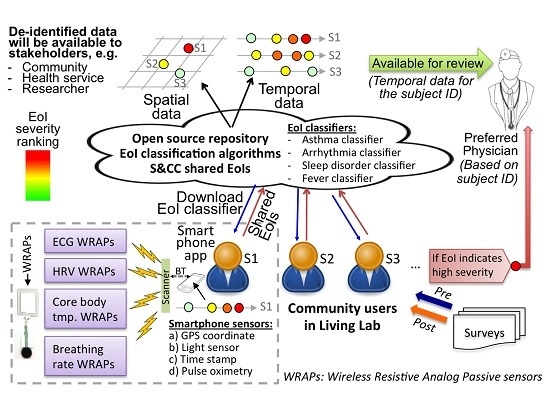
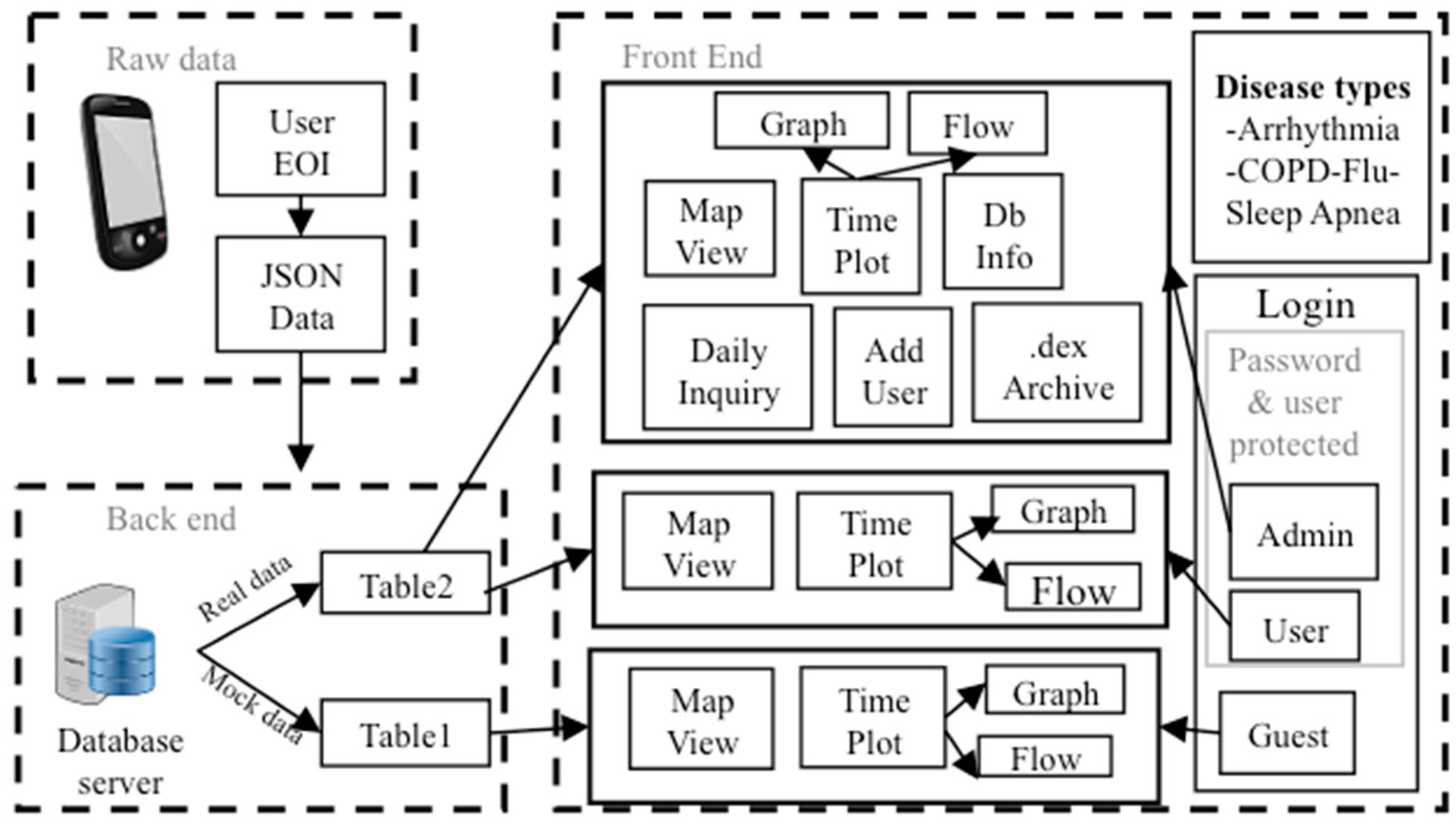
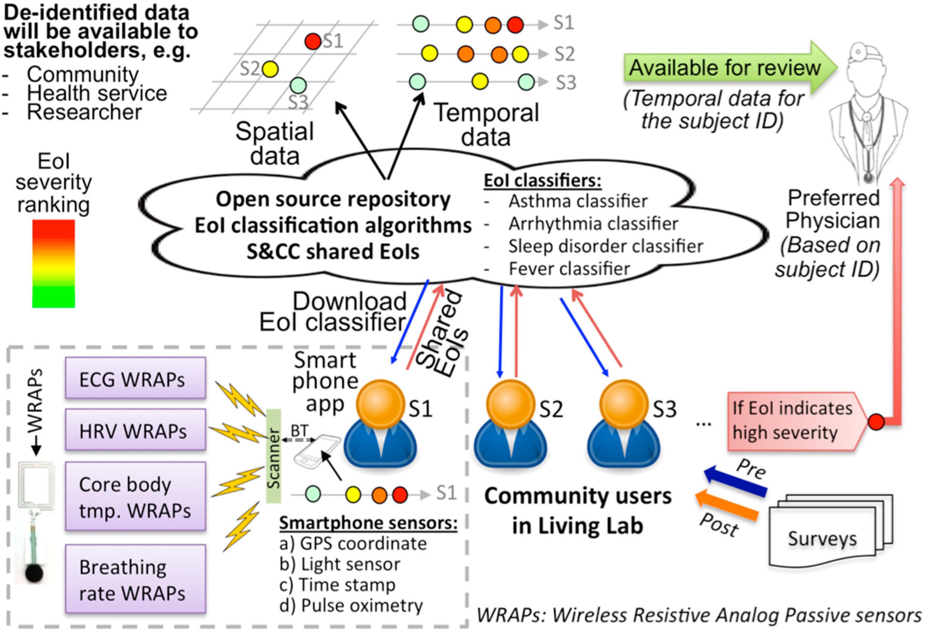
2.1. A. Overall System Description

The framework consists of the WRAP sensors for physiological data collection, a scanner to capture data, a smartphone app for computation of disease related Events-of-Interest (EoI) using real-time classification algorithms, and anonymous EoI submission to a custom SCC Health web-server for collective community health knowledge gathering and dissemination. The system will be deployed in a pilot study to collect user submitted EoI information anonymously for various health conditions and visualize the EoIs in spatial and temporal domains on the SCC Health web-server. The users will also participate in pre- and post-session (30-days) surveys regarding acceptability, wearability, usability, and related concerns. A conceptual diagram of the complete system framework is presented in Figure 1.
As the system will be studied with human subjects, an Institutional Review Board (IRB) approval was obtained. The IRB rules consider the device safety, usage, protocol, recruitment, and consents. The IRB was approved through the University of Memphis IRB committee (Approval Number: PRO-FY2017-474).

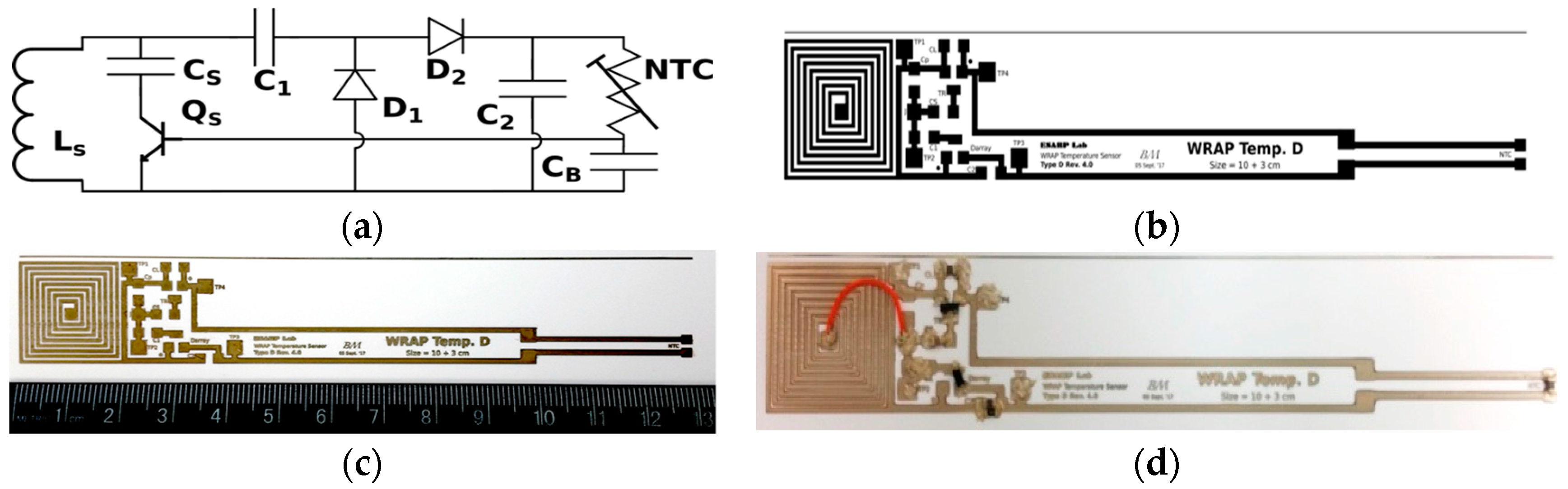
2.2. B. WRAP Sensor Operation Theory

The fully passive wireless sensor does not require its own power source; rather it utilizes the incident power from the wireless carrier signal of the scanner [36]. There are two approaches for this sensor design: magnetic induction suitable for near field, and RF backscattering suitable for far field [12]. In magnetic induction, the sensor receives the wireless signal, and modulates the carrier wave that is sensed by the scanner as a small change of voltage across or current through its coil. In backscattering, a portion of the RF signal from the scanner reflects from the dipole antenna of the sensor, depending on radar aperture size [10]. However, for body-worn sensors, inductive loading is a more appropriate solution due to non-ionizing radiation and proximity of the portable scanner to body-worn sensors [36]. For the simple WRAP sensor system [37,38], the effective impedance from the scanner side correlates to load resistance (RL) of a RLC parallel circuit, and is given by:
Z T x = X R x + j w L T x 1 j w ( C T x ) R T x
where
X R x = ( w M ) 2 Z R x
and
Z R x = j w L R x 1 j w ( C R x ) R L
Here, Z represents impedance, X represents reactance, M is the mutual inductance, and Tx is the primary (scanner) related whereas Rx is secondary (sensor) related parameter. For inductive loading, the ωr (=2πfr), the angular resonance frequency of the RLC parallel circuit, is given by [33]:
ω r = 1 L C ( R s L ) 2 .
Here R, L and C are the parallel resistance, inductance and capacitance, respectively, and RS is the intrinsic resistance of the impure inductor. For WRAP sensors printed with IJP, the sensor intrinsic resistance is significantly higher (e.g., for Ag ink used in this report, the average resistance of secondary coil for the given design was 21 Ω). For such systems with intrinsic resistance of primary and secondary coils (RS1 and RS2, respectively), the overall efficiency ( η ) of the inductive link can be given by [52]:
η = R r e f R r e f + R S 1 × Q 2 L Q L
where Rref is the reflected resistance from secondary to primary side, and can be expressed as:
R r e f = k 2 R S 1 Q 1 Q 2 L .
Here, k is the coupling factor between two coils, and Q1, Q2 and Q2L are the quality factors of primary, secondary without load, and secondary with load, respectively, and can be expressed as Q 1 = L 1 ω R S 1 ,   Q 2 = L 2 ω R S 2 ,   Q L R L L 2 ω ,   and   Q 2 L = Q 2 Q 2 + Q L . Here L1 and L2 are inductances of primary and secondary coils, respectively. For high sensitivity of the sensors, coil design should be optimized to maximize η [52].
The WRAP sensor design is such that the signal to be probed will cause change of RL. For instance, RL can be simply transducer resistance [37], or the resistance across a transistor [38,39] used to probe bioelectric or impedimetric signals. The carrier signal amplitude is modulated due to change of RL, and the modulated signals at the scanner correlate to the changes of RL. We have previously describes WRAP sensors based on this technique for physiological signal collection and bio-potential signal capture [37,38,39].
While this technique is useful for signals where the information is encoded differentially (e.g., heart beat signal only needs to identify the times when peak occurs, the absolute value is irrelevant), some signals contain information in absolute magnitude (e.g., body temperature). Absolute magnitude data collection is more challenging for WRAP sensors as the absolute magnitude of impedance loading is influenced by many factors such as modulation index, coil separation, and permeability of the medium, that can change at the time of deployment. Previously we have described a duel coil approach to collect absolute magnitude values from WRAP sensors [53]. However, the approach requires higher bandwidth due to use of a reference coil.
Here, we describe a new approach where the absolute magnitude value is encoded in time domain rather than magnitude. This is robust against artifactual variability, as those do not influence time domain change. Mathematically, this can be represented as f ( A ) T f ( t ) . To explain this, let us consider the schematic of a new WRAP temperature sensor (Type D) circuit shown in Figure 2a that transforms the signal change (temperature) to time domain (time delay) for higher sensitivity. The WRAP temperature sensor consists of an inkjet printed inductive coil, Ls, and a circuit consisting of discrete electronic components. The capacitor-diode pairs of C1-D1 and C2-D2 constitute a two-stage voltage doubler. The voltage is applied across a NTC (Negative Temperature Coefficient) temperature sensor and a capacitor, CB, which forms an RC time delay circuit. This causes the base voltage of NPN transistor Qs to be turned on after a certain delay. When turned on, Qs loads the inductive coil, Ls, with load impedance, Cs, in combination with the emitter–collector (on) resistance of Qs. This loading effect can be detected at the scanner coil as a signal transition, and the corresponding time delay can be calibrated with the temperature of NTC. The resistance (RNTC) of the NTC at ambient temperature (T) is given by:
R N T C = R 0 e x p B ( 1 / T 1 / T 0 )
where R0 is the resistance at ambient temperature T0 and B is the constant of thermistor given by,
B = l n   ( R / R 0 ) / ( 1 / T 1 / T 0 ) .
Hence, time delay (δ) for RC to charge by 63.2% can be expressed as,
δ = R N T C C B = R 0 C B e x p B ( 1 / T 1 / T 0 )
This nonlinear function will inversely relate temperature with the time delay, and can be decoded by simple linear regression analysis. However, due to the fact that the modulation index is a function of many factors (such as distance, displacement, and orientation between coils, permeability of the medium), the induced voltage at the sensor coil might vary and might change the transition time delay. The induced voltage also relates to the amount of voltage swing before and after transition. Thus, a more complex nonlinear classifier is needed for accurate measurement of temperature.

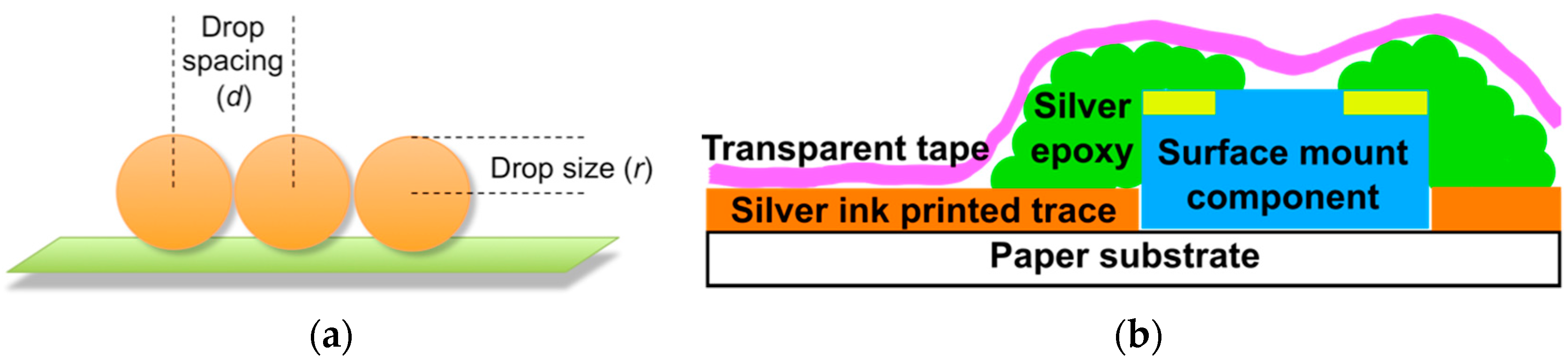
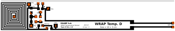
2.3. C. Inkjet Printed WRAP Sensors

The sensor layout, shown in Figure 2b, was generated with Inkscape software (freeware) in svg file format. In most electric circuit designs, a single layer is not sufficient and one or more jump wires are needed. This is a constraint for planar fabrication processes such as inkjet printing techniques. Effort was taken during the layout design to minimize the number of jump wires. After layout design, the svg file was exported to png format with a resolution of 1693 dpi to match the printer resolution. The png image was then converted to 1-bit monochrome bmp file format using Paint (Microsoft Corp., Redmond, WA, USA). This file was then imported by the printing software (Dimatix DMP tool) and converted to ptf format that can be printed with the inkjet printer (Figure 2c). The component population complexity and cost directly relates with the number of components, hence an effort was made to minimize the component requirement as well.
This WRAP temperature sensor (as shown in Figure 2a) requires 7 discrete components of 2-pins, and 1 discrete component of 3-pins, and 1 jumping wire. The component selected for Qs is MMBTH10, D1 and D2 are CDBF0130L, NTC is NCP21XV103J03RA (10 kΩ), and the values of capacitors are C1 = C2 = 0.47 µF, CB = 0.1 µF, and Cs = 0.22 µF (Figure 2d). The designed sensors shown are 13 cm long; however, the length is customizable (by extending the tail portion of NTC trace). The actual size for deployment can be individually tailored to the user's exact measurements and preference. The NTC sensor will be placed in the armpit, while the coil can wrap on top of the arm or chest—depending on the user’s choice.
The thicknesses of the IJP Ag traces are in the range of 1 µm to 2 µm, which can be manipulated by altering the drop size and drop spacing (Figure 3a). Increased drop size will result in thicker trace and vice versa. Printing of a thinner trace layer might lead to discontinuity, as ink tends to accumulate due to surface tension, while printing a thicker layer leads to a higher tendency to self peel-off due to mismatch of stress of the trace with that of the substrate. Hence a tradeoff must be made for the particular ink and the engineering needs. The entire process of a functional circuit development using IJP is schematically depicted in Figure 3b. The first step of the process is to print the silver traces on the paper substrate. After printing of the silver conductive trace using the printer, the ink is allowed to dry at room temperature for 5 min. Then, surface mount device (SMD) components are placed on the substrate at the required positions. An electrically conductive silver epoxy mixture is applied for connectivity between the printed trace and the SMD component pins. The silver epoxy is then cured with forced air for 24 h.
The printed WRAP sensors were developed by depositing conductive thin-film traces of silver nanoparticles on paper substrate (glossy photo–paper, 10.2 mil) on the glossy side utilizing a material deposition printer (Dimatix DMP-2831, FujiFilm Dimatix Inc., Santa Clara, CA, USA) using a ~40% loaded silver nanoparticle-based ink (Metalon JS-B40, Nanosilver Ink, Novacentrix, Austin, TX, USA). These printings were performed with 10 pL cartridges from Dimatix and all 16 nozzles were used for printing. The average sizes of the Ag nanoparticles were between 85 to 115 nm. The printing ink viscosities were between 3 to 10 cPa with 30 to 50% loading. The drop spacing of the printer was kept at 15 μm by setting the printer resolution to 1693 dpi. The trace widths for electrically conductive silver nanoparticle thin film were between 0.2 to 2.5 mm, as narrower traces had a higher tendency to result in discontinuity while wider traces led to self peel-off phenomenon. Relief cavities can be placed every 2.5 mm to reduce this self peel-off tendency.
The discrete surface mount devices (SMD) were electronically attached to these silver (Ag) traces on paper using low-temperature curable silver epoxy (8331S, MG Chemicals, Surrey, BC, Canada) with 1:1 of Part A and Part B. The components were cured for 24 h under forced air. Paper substrates cannot tolerate temperature curing process (~180 °C) or even low-temperature soldering (~137 °C).

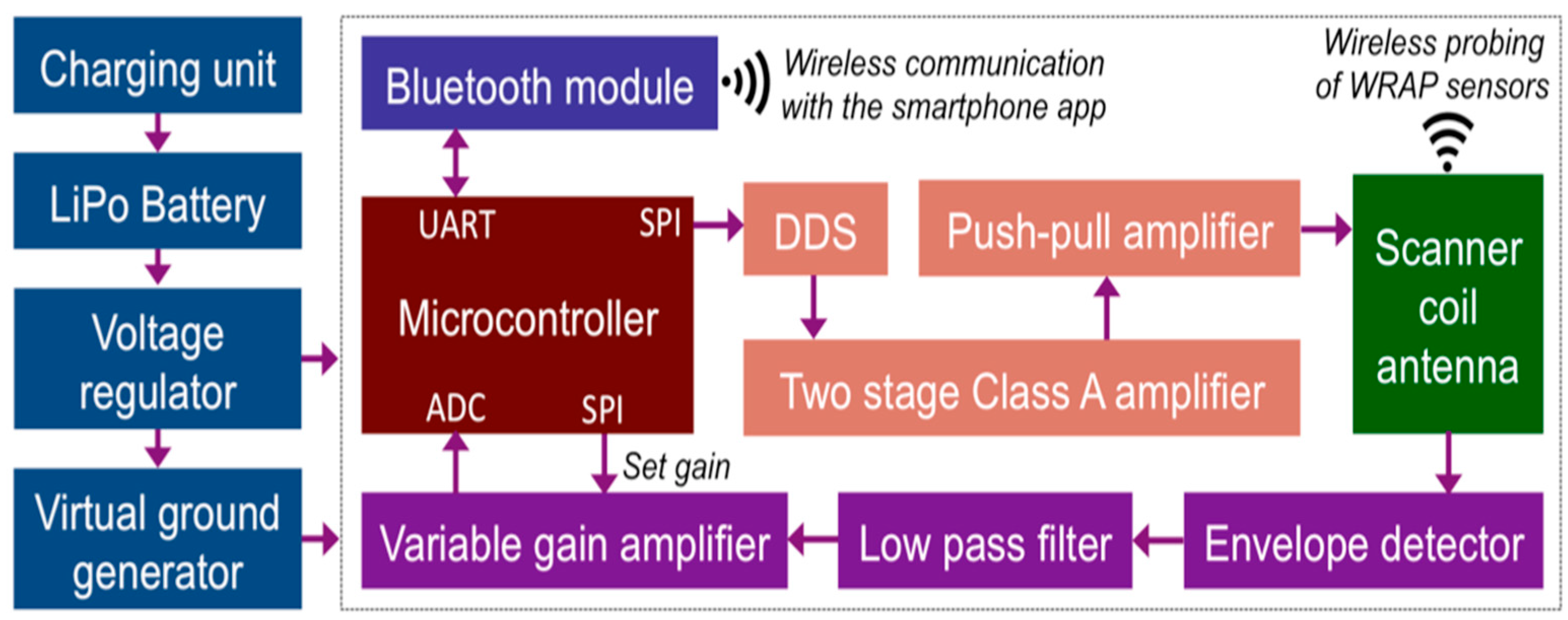
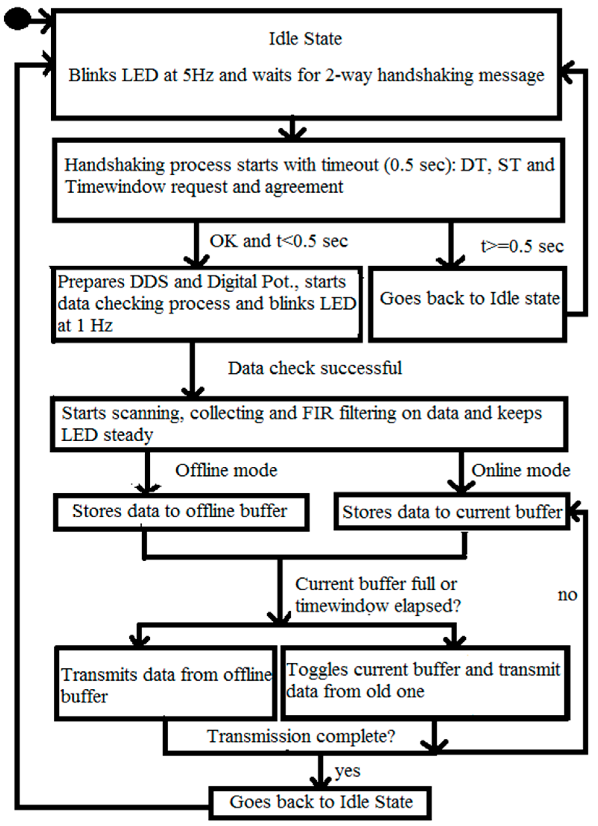
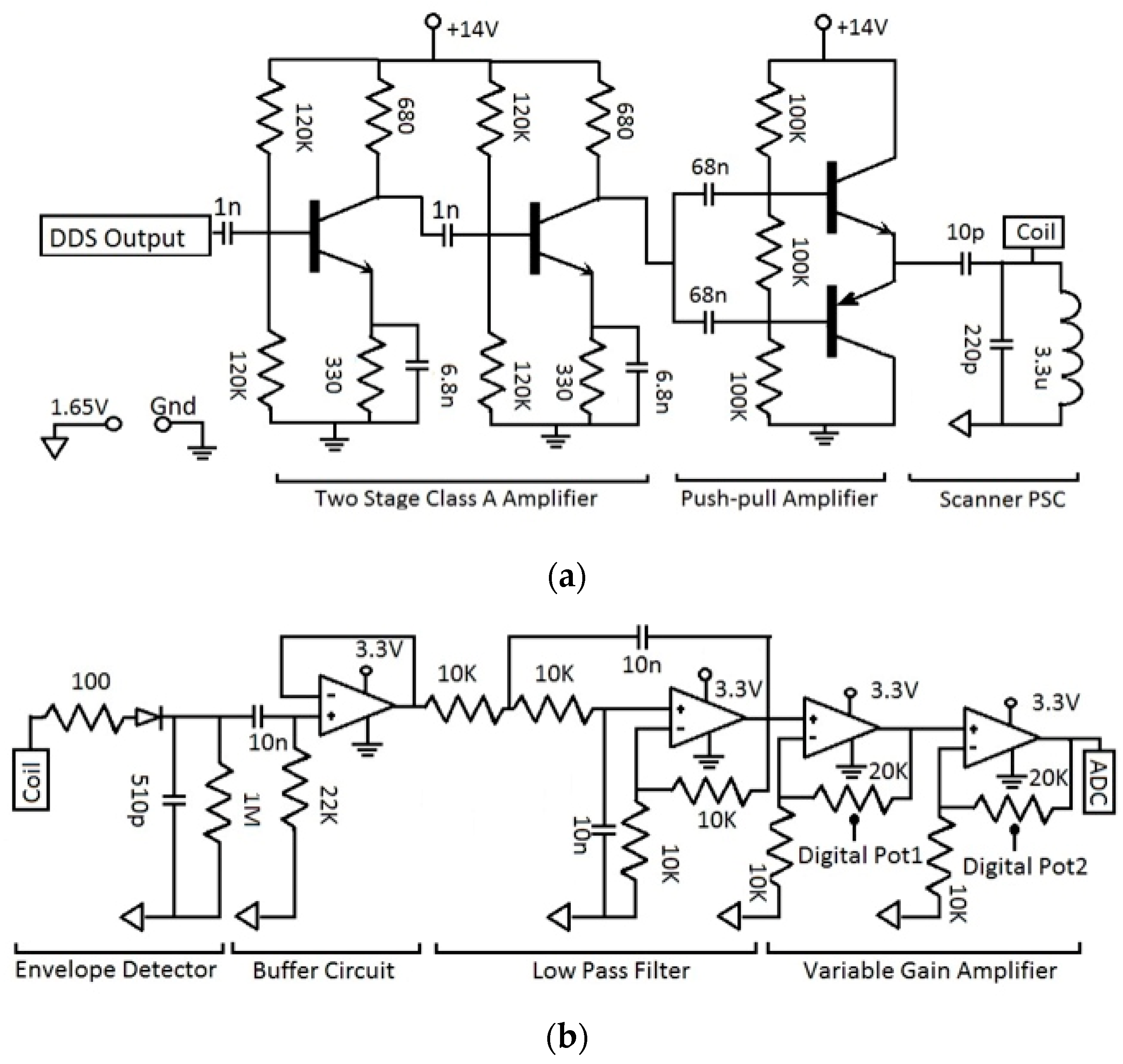
2.4. C. Wearable Scanner

The scanner device was prototyped in-house using embedded system technology. The schematic and PCB design was developed with Cadence Allegro software (Cadence Design Systems Inc., San Jose, CA, USA). The PCB was fabricated via OshPark fabrication service (https://oshpark.com/). The design contains an ultra low power microcontroller unit (MCU) from ST Microelectronics, a RF synthesizer, a transmit chain, a circulator T-junction, a loop antenna, a receive chain, a RF synthesizer, and an envelope detector. The hardware also has a power management unit, and a wireless (Bluetooth) communication unit compatible with smartphones.
The scanner board is controlled by a 32-bit low power flash microcontroller (STM32L476, ST Microelectronics) based on ARM Cortex-M processor (Figure 4). The microcontroller can request a 50 MHz low power Direct Digital Synthesizer (DDS) device (AD9834) to generate the required carrier wave in RF range. The scanner will use 13.56 MHz (ISM band) wireless signals in small burst mode (<1 ms) to capture signals from WRAP sensors. AD9834 can synthesize tones up to 37 MHz. However, at this prototyping phase, due to component mismatch, the maximum resonance frequency is observed to significantly deviate from this designed frequency, which will be addressed in subsequent revisions of the scanner design. The amplitude modulation of the carrier signal by the WRAP sensor is detected via an envelope detector followed by a low-pass filter. There is also a microcontroller controlled variable gain amplifier (VGA) to dynamically scale the signal in analog domain to maximize fidelity of ADC.
The scanner coil picks up the top envelope of the amplitude modulated signal by using an envelope detector with a Schottky diode, processes the signal first in analog, and later in digital domains, and finally transmits it to the smartphone appication (app) via a Class 2 Bluetooth module (RN-42, Microchip Technologies Inc., Chandler, AZ, USA) at 115.2 kbps using Serial Port Profile (SPP). The scanner analog circuit schematic is shown in Figure 5. The DDS output is first amplified with a two-stage Class-A amplifier and fed to a push-pull driver amplifier. To produce the required wiereless transmission energy, a 14 volt supply is used for this stage that will be generated with a voltage booster chip. The amplified RF carrier signal is fed to a Printed Spiral Coil (PSC) that we have previously optmized [52,54].
The modulated signal is also captured from this PSC and fed to an evelope detector composed of a diode and a capacitor. A buffer stage (realized with LMV792 dual opamp) follows to ensure that the evelope detector is not loaded by subsequent stages. A 2nd order Butterworth low-pass filter (cut off frequency of 1.5 kHz) minimizes high frequency ripple. The signal is then amplified (using MCP6002) with a two stage variable gain amplifier (VGA) (realized with AD5262) whose gain can be controlled by the microcontroller at run-time. These Digital Pots will allow us to maximize the analog signal to fit the ADC range for superior resolution. MCP6002 has a large Gain Band-Width product (GBW) compared to the RF signal that we are measuring, hence the gain can be increased significantly without instability. Finally, the analog signal is sampled by the 12-bit sigma-delta ADC of the microcontroller. The ADC sampling rate is 30 ksps.
The ADC is triggered by a timer to capture samples of analog signals, and the sampled data is then processed by the firmware. The firmware sequence diagram is shown in Figure 6. The sampled data from the ADC port first needs to be placed to the software buffer that maintains this constraint to safeguard against any data loss. The timing guarantee of ADC data fetch was guaranteed with a timer driven interrupt service routine (ISR) approach. We have implemented a mutex-buffer pair to resolve data overflow issues. Before inserting the data into the buffer, the ISR checks if the buffer is full. If the buffer is full, the active buffer is toggled and the full buffer data is sent to the app via Bluetooth (BT). The ISR also checks if the buffer is partially full when the requested time elapses, and in that case, transmits only that portion of the buffer. The data is transmitted to the BT through Universal Asynchronous Receiver Transmitter (UART) port of the microcontroller. The scanner board uses an LED indicator that turns on or blinks at various rates to indicate different stages, functioning (e.g., idle state, scanning state, and transmission state), or error of the firmware. The microcontroller is set to idle state if no activity is requested. The microcontroller wakes up when the app requests a data collection event. We have incorporated a custom double-handshaking protocol that allows the app to transmit the required information such as disease type (DT), sensor type (ST), and time duration of data collection (Timewindow). This information allows the scanner device to initialize. Then, it collects data from the WRAP sensor and transmits the data to the app.

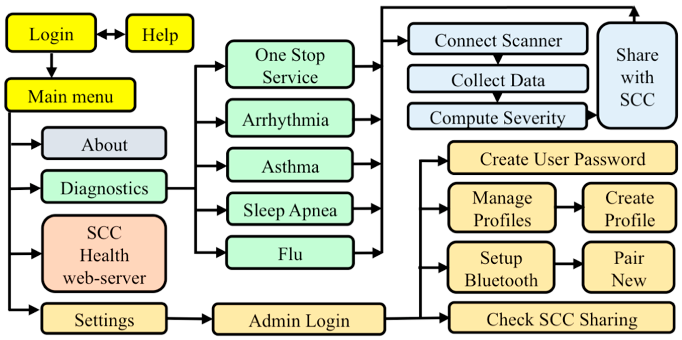
2.5. D. SCC Health Smartphone App

An Android based smartphone app was developed to collect data from the scanner, and to locally process the physiological signals using the EoI classification algorithms. The computed EoI severity will be displayed on the phone, and the user will have an option to submit the anonymized EoIs to the SCC Health web-server. A sequence diagram of different elements in the app is depicted in Figure 7. An SQLite database is used in the app that stores date and time of the test along with disease severity. It can help the physician to analyze the data for the particular disease condition at a later time, and will be directly transmitted to a medical doctor via SMS in case a very high severity is detected (see Figure 1).
For severity (EoI) computation, algorithms must be incorporated in the smartphone app to perform real-time computations. As an example, the temperature EoI computation is described here. At first, a medical doctor was consulted to understand the clinical severity of various core-body temperate (fever or flu). Based on the information, a text based severity label has been assigned to different ranges, e.g., temperature from 100.4 °F to 101.9 °F is assigned to “Low grade fever”. A complete list is provided in Table 1. To compute this core-body temperature, the auxiliary temperature data from the armpit sensor needs to be incremented by 2 °F. Furthermore, the medical doctor also provided notes for various temperature ranges (with 1 °F granularity) as shown in Table 1 that display the temperature and notes in the smartphone app based on user's core-body temperature. Using this information, EoI computation algorithms for flu were developed. For instance, a linear scale algorithm is shown in Table 1 where the lowest possible body temperature (97 °F) is assigned as EoI = 0, and maximum possible temperature (107 °F) is assigned as EoI = 1. Any temperature above 105 °F is considered extreme fever and 107 °F is considered a medical emergency. For these ranges, an alert will be displayed for the patient to seek immediate medical attention (e.g., ER) as well as a direct SMS can be transmitted to the medical doctor. As such, for flu EoI, the threshold for alert is set at 0.8 or above.
This algorithm will be stored in the server for download by the app when needed. As we develop this framework, in future, we will open the framework to researchers to submit their algorithms (which will go through a small validation phase with representative labeled data for classification to allow detection of unacceptable algorithms). Thus, users will be able to download various algorithms as needed. For instance, we have also developed a log-scale ranking for Flu severity computation. Both algorithms are available for the user to choose at the time of severity computation. The algorithms will be stored in the server in dex format, which can be accessed from the app when downloaded in the smartphone. The process will be a seamless experience for the user through a single click of a button.
For visualization purposes, we have assigned a dark green color to EoI = 0 (minimum), and dark red to EoI = 1 (maximum). The EoI color representations are graded based on the image shown in Table 1. The exact same color pallet is used in the SCC Health web-server for consistency. The color of EoIs provides a visual of severity that users can easily relate to.

2.6. E. SCC Health Web-Server

For visualization of submitted anonymized EoIs, we have developed a SCC Health web-server where submitted data are automatically stored in a database and can be interactively queried by users. The interaction diagram of the SCC Health web-server is shown in Figure 8. The EoIs computed from users' sensor data are formatted as JSON data when shared with SCC Health web-server. When the server receives this JSON data, it parses the required information to store in the server database. In addition to EoI value, this information also includes area code, disease type, timestamp, and patient ID number. The area code is assigned to each user based on their home address. This area code is arbitrarily generated at the time of grid assignment during the planning phase. All homes inside a grid will have the same unique area code. This adds a layer to privacy, as it is not possible from the visualization, or even the server data, to identify the user's exact home location.
After careful consideration of different visualization possibilities and scenarios, we have selected an arbitrary subject number with EoI severity change for temporal view and a grid method overlaying Google map for spatial view. Users will be able to visualize their own data from the smartphone app, but when they log in to the SCC Health web-server to visualize community data, they will not be able to distinguish their own data from others. In the temporal view, the users can select a date range and the type of disease, and can see the data in traditional graph format (where y-axis represents severity of the disease) or in flow format (where the color represents severity). In both temporal view options, the data depicts health status of the community members over time. The temporal flow plot shows the progression of disease (as per selection) on individuals (encoded with severity color code) over time (as per selection) that can identify worsening or improving overall community health.
Spatial data visualization via SCC webserver (e.g., Google Map overlay for spatial distribution of EoIs) is such that a subject’s exact location will not be identifiable to preserve privacy and confidentiality. The grid allows us to hide the exact location of the data submitter as a user can be located at any location within that grid (as opposed to circular representation, whose center can be determined). Furthermore, data within a grid is dynamically averaged using the following formula to determine overall severity (EoI) of the selected disease for the selected date range for that grid:
E o I a v i = 1 N u = 1   t o   N ( 1 M j = 1   t o   M E o I i , u , j )
where i is the grid number, u is the user number, N is the maximum number of users in that i-th grid who submitted EoIs for that particular disease within that timeframe, j is the number of times user u has submitted EoIs within that timeframe, and M is the maximum number of EoI submission of that user. During visualization, RGB codes are pre-computed for 101 discrete levels according to the color scheme given in Table 1, and EoIs are scaled and rounded from 0 to 100.

3. Results

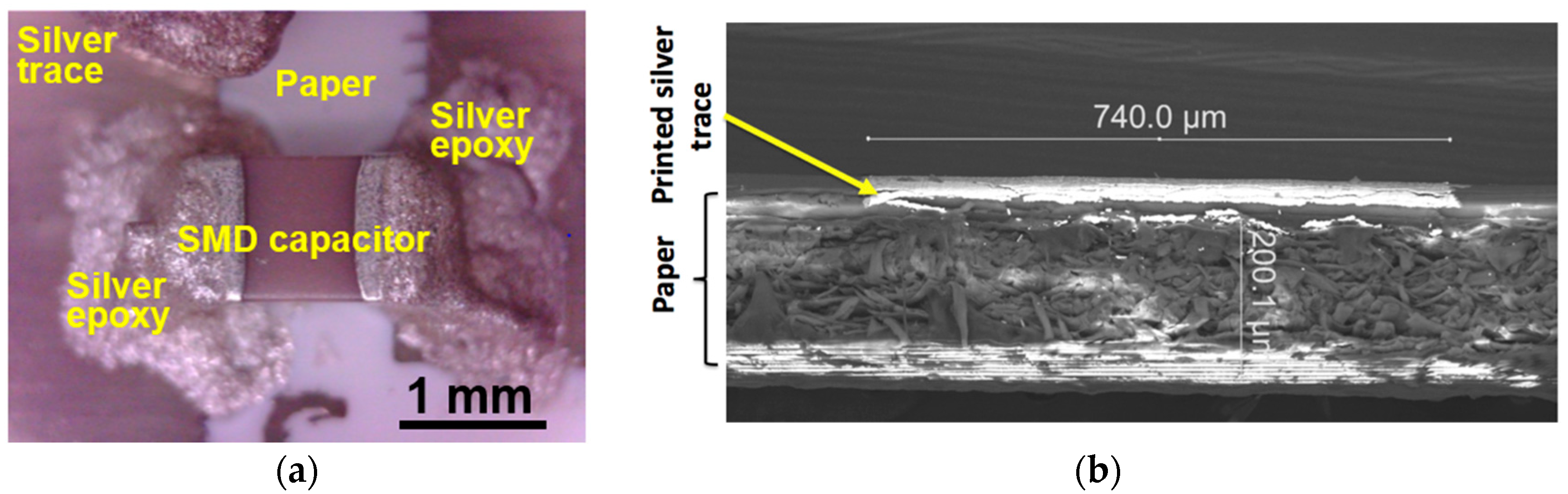
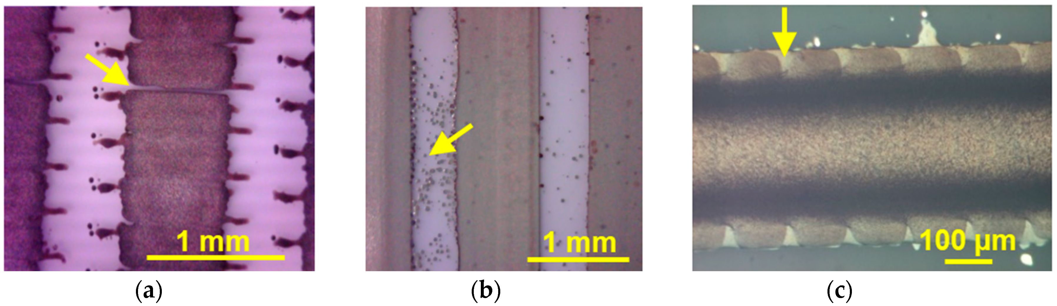
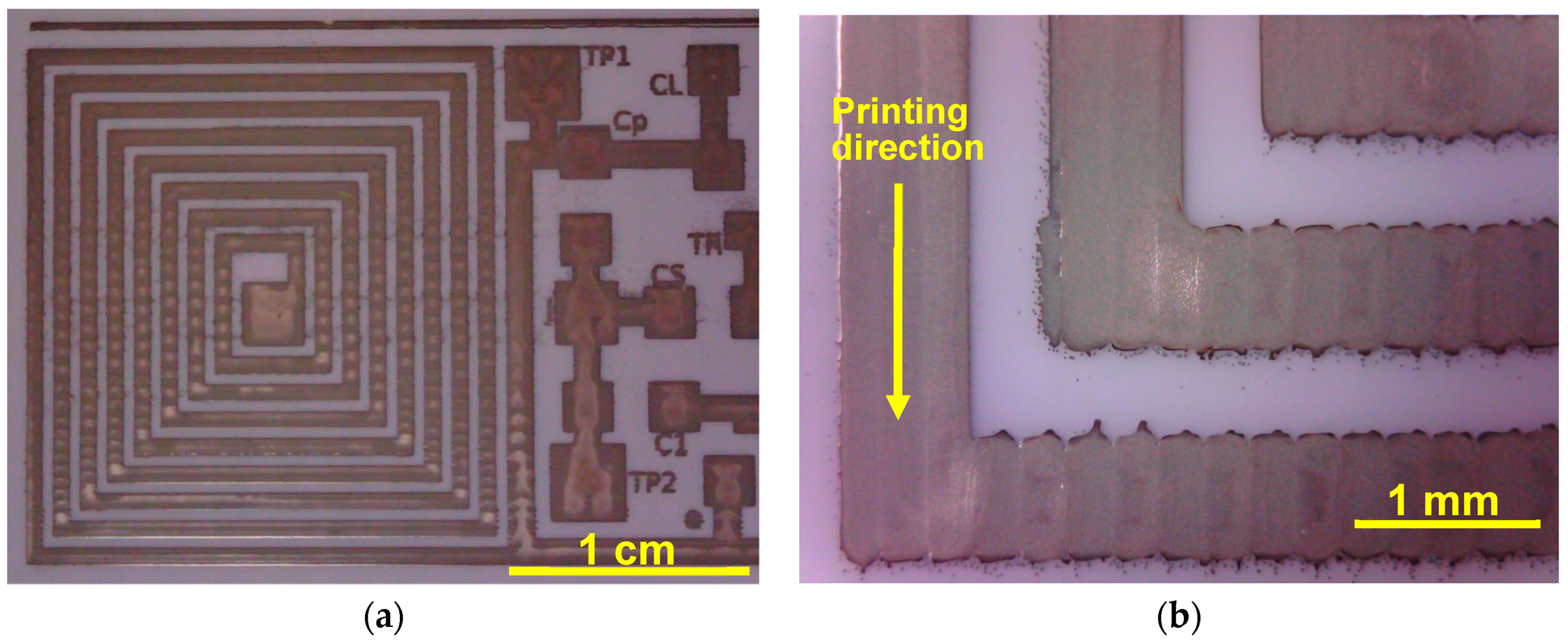
3.1. Printing Related Results

The printed WRAP temperature sensor on a paper substrate after drying of ink and after population of components is shown in Figure 2b,c. As this printer uses a MEMS based cartridge with precise droplet size (20 pL) and high resolution (20 µm), the printed sensors are sharply defined and consistent in deposited material properties (e.g., uniform thickness of traces). However, observations under optical microscope show interesting details of these IJP traces of the WRAP temperature sensor (Figure 9). For instance, although the IJP traces are observed to be crisp, higher magnification depicts characteristic imperfections of trace edges when the trace is in perpendicular direction to the printing direction (IJP cartridge prints along the direction shown). This imperfection of edges does not cause functionality issue.
More importantly, the Ag traces of IJP technique shows higher resistivity compared to copper (Cu) traces of traditional PCB, which degrades performance of the circuit at higher frequencies (e.g., RF frequency for WRAP sensors). The IJP traces with Ag B40 ink on paper substrate have a thickness between 1 to 2 µm and the average sheet resistivity was 21 mΩ/square, while the resistance of the printed loop antenna was 21 ± 3 Ω. The resistances of printed silver traces as measured between various pads (as indicated on the layout) are given in Table 2. These values are more than an order higher than typically observed for PCB (Cu traces) values. The increased resistances of traces have detrimental effects for WRAP sensors such as reduction of quality factor and increase of RF noise.
The population of components is performed with silver epoxy. An optical microscopic image is shown in Figure 10a depicting this silver epoxy connection of a discrete SMD component on an Ag trace printed on paper. Figure 10b shows a Scanning Electron Microscopy (SEM) image of a cross-sectional view of an Ag trace on a paper substrate. The thickness of paper substrate is 200 µm and the height of SMD components selected were less than 0.8 mm to keep the total thickness of the prototyped sensors to less than 1 mm.
Being a new technology, utilizing IJP is expected to encounter a variety of prototyping issues that need careful consideration during fabrication. Some of these issues can cause open or short of the traces leading to non-functional circuit. For instance, the inkjet printing process might lead to micro-gaps resulting in discontinuity (Figure 11a). Manipulation of the ink printing profile, such as drop-rate, can reduce probability of this type of error. For instance, we have found that printing at 10 kHz drop rate leads to a higher yield compared to printing at 80 kHz as prescribed by the ink manufacturer. However, printing at the lower rate increases the time required for printing. Other issues include misfired droplets due to partially blocked nozzles or accumulated ink near the nozzle opening of the cartridge (Figure 11b). In worst cases, this can lead to shorts between adjacent traces. The nozzle surface was wiped clean with ethanol dipped fibreless wipes. In addition, sufficient spacing of traces must be maintained to avoid shorting issue. Through numerous prototyping and testing experiments, we are forming a set of design rules for IJP on paper substrates (e.g., for 40% loaded Ag, our design rule is minimum trace width = 0.5 mm, minimum gap between traces = 0.4 mm, and maximum trace width = 2.5 mm). Figure 11c shows the rugged edges of the printed traces, resulting from drying of ink from fluidic state and accumulation of inks at the center of the trace due to surface tension. Although this does not affect functionality of the circuit, a quick drying surface or rapid sintering process can reduce this imperfection.

3.2. Wearable Scanner Device

The power consumption by the wearable scanner board is an important consideration for long duration of operation. The power consumption is tabulated in Table 3. The most power is consumed by the analog driver amplifier consisting of the two-stage Class A amplifier and the push-pull amplifier. Class A analog amplifier consumes 9.5 ± 0.5 mA while the push-pull analog amplifier consumes 18.5 ± 0.5 mA. The total power consumption during scanning is ~500 mW. For WRAP temperature sensor of Type D, the scanning can complete within 100 ms, hence energy consumed per scan is as low as 50 mJ.

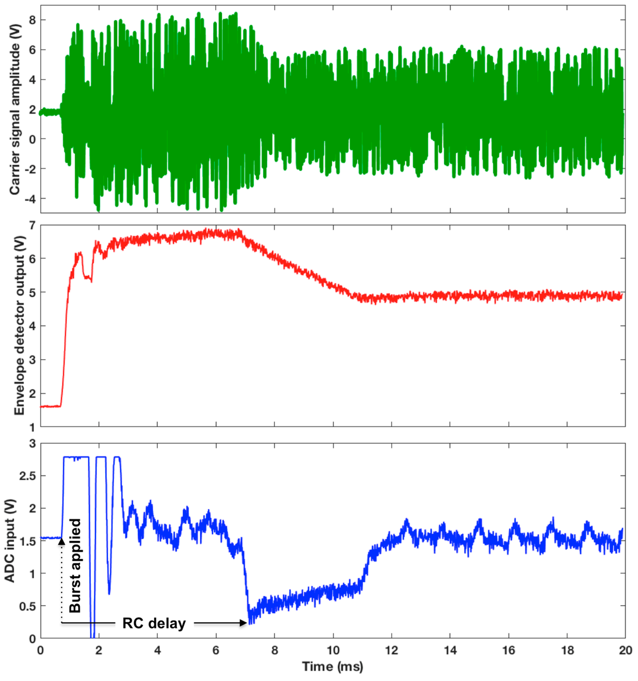
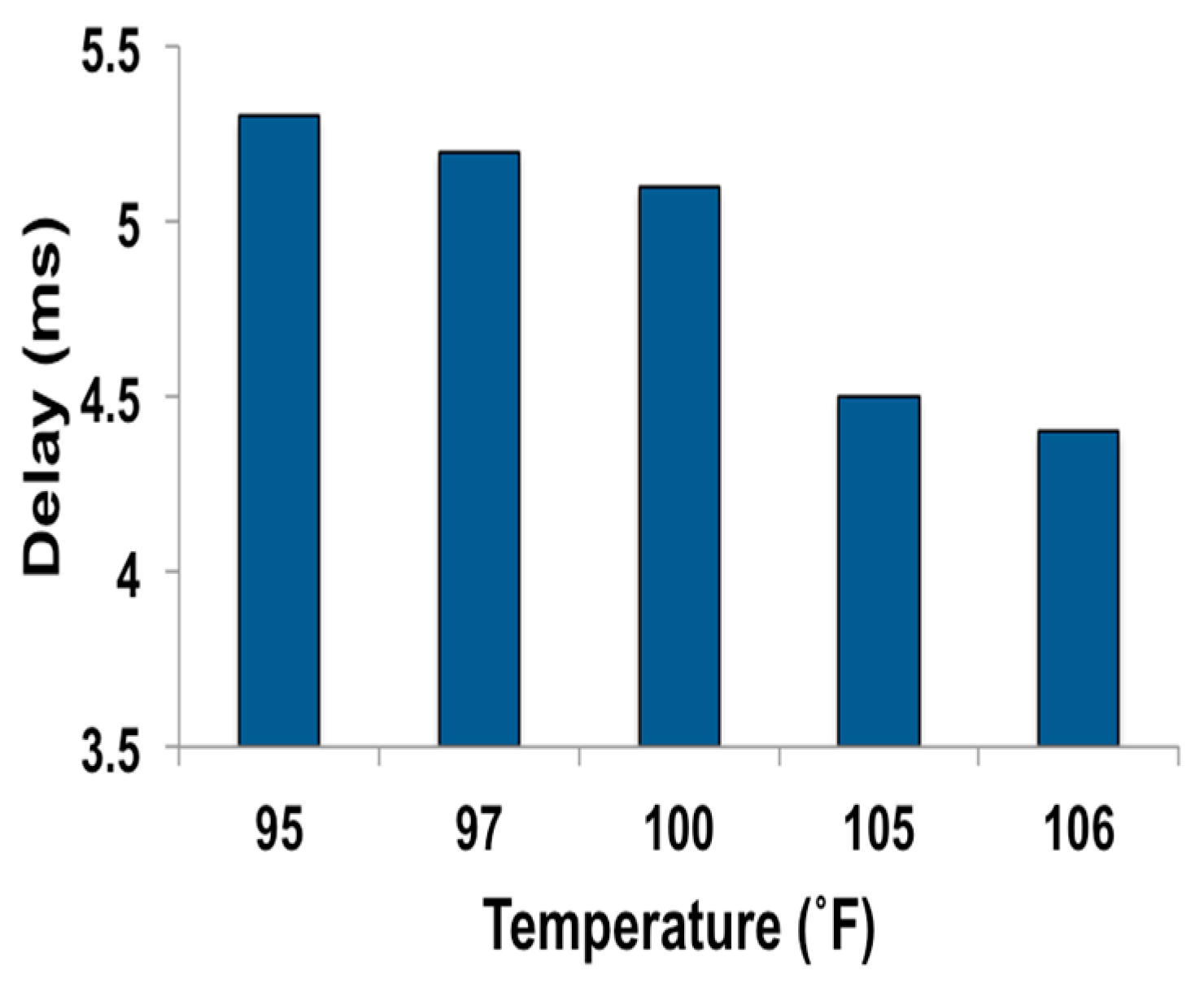
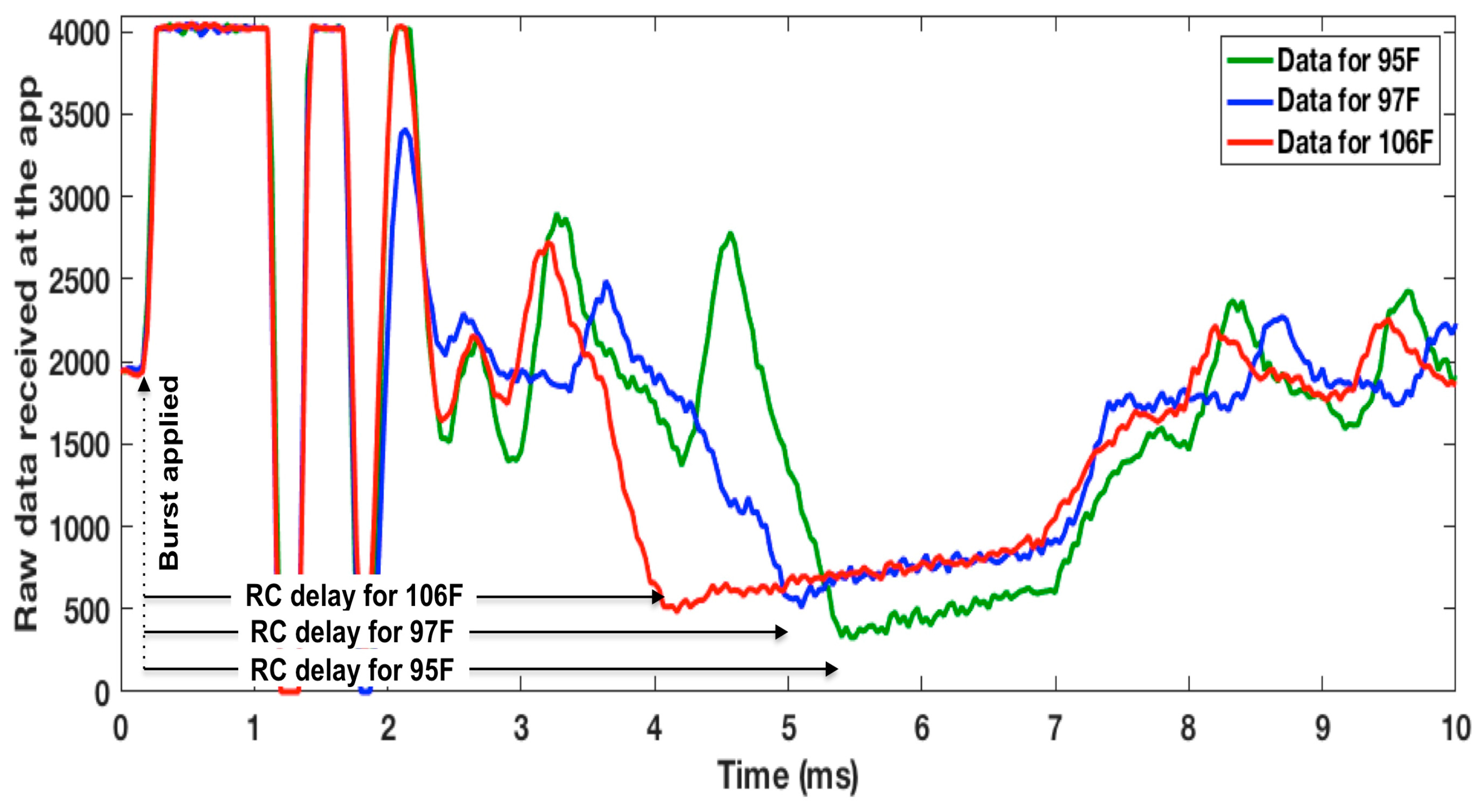
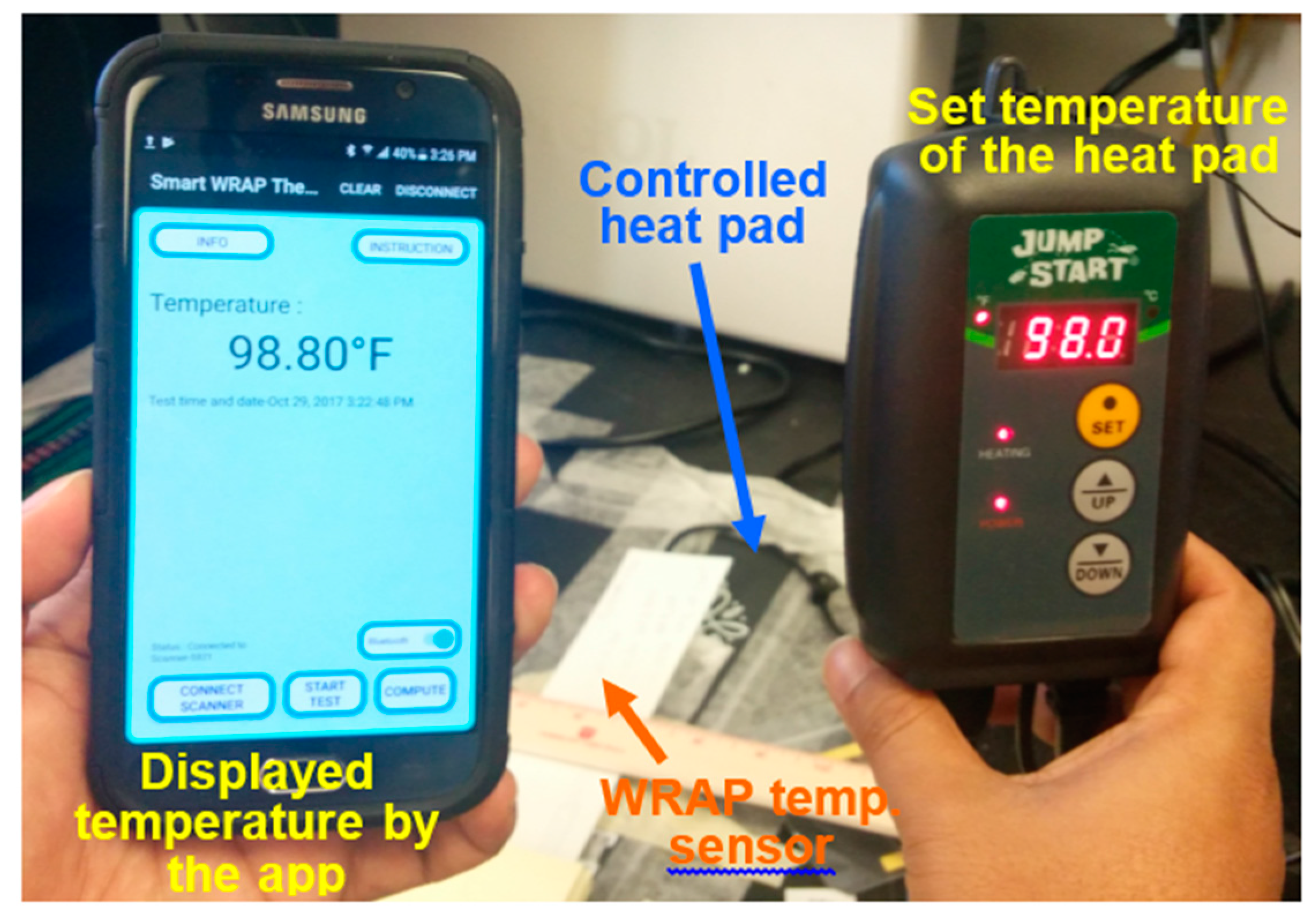
3.3. WRAP Sensor Test Results

The WRAP temperature sensor functional test setup is shown in Figure 12. The setup consists of a controllable temperature pad, a WRAP temperature sensor, a scanner prototype, a power supply, and an oscilloscope for signal probing at the ADC. Constant temperature was maintained with a temperature control module (iPower Heat Mat and Digital Thermostat Controller) that allows a controllable range from 68 °F to 108 °F. The NTC was placed on the mat, whereas the sensor coil portion is laid on the scanner coil. A burst of 1 s signal was applied and data was collected for the first 10 ms for further processing.
The WRAP temperature sensor Type D causes a transition of carrier signal by turning on the after a time delay set by RNTC (a function of temperature) and a fixed capacitor CB as described in the WRAP sensor theory section. To capture data from the sensor, a burst of 100 ms of the carrier signal is applied by the scanner device. Figure 13 shows the signals the carrier signal being generated by the DDS when the burst is applied (triggered by the microcontroller). The envelope of the carrier signal (top) changes at the time of transistor switching on after the time delay, which is a function of RNTC. This causes the envelope detector output to decrease at that time. This transition, after the analog filter and signal conditioning stage, causes the input signal at ADC to show a characteristic dip. Change of carrier amplitude after the RC time delay is apparent, which correspondingly causes signal transition at the envelope detector output and the input of the ADC fed through the analog signal conditioning circuit. The amplitude shift at the envelope detector results in this signal transition (dip) due to capacitive coupling and LPF. After digitization of this analog data by the ADC, data is transmitted by the microcontroller in the scanner board to the smartphone app via Bluetooth module.
A temporal plot of the received data at the smartphone app for different temperatures is shown in Figure 14. Clear distinctions of transition times (dip observed as the lowest points of the curves) are observed for different temperatures. This inverse nonlinear relationship is clearly observed. The start time depends on the RC time delay. The app can use a minima function after the initial transients to identify the time delay. A representative data collection snapshot is provided in Figure 15 that shows the set temperature of the heat pad using the controller (98 °F) and the detected temperature by the smartphone app (98.8 °F). The error is within tolerance of 1 °F, but we will further calibrate the system to reduce errors, for example by incorporating other prominent signal feature such as duration of the dip. Figure 16 shows a plot of various RC time delays captured for a range of temperature validating the functionality of the developed WRAP temperature sensors. An inverse relationship is observed with delay time (from the application of the pulse and the lowest point of the dip) and the corresponding temperature. This inverse relationship is expected due to the nature of NTC. This shows the proof-of-concept functionality; however this sensor is currently being further investigated for full characterization to determine the resolution and accuracy using complex machine learning algorithms.

3.4. Functional SCC Health App

Representative snapshots of various app graphical user interfaces (GUI) are shown in Figure 17. The app allows the user to connect to the portable scanner (via Bluetooth pairing), determine the WRAP sensor to be used for a particular disease, allow collection of data from the sensor, compute severity (EoI), and allows the user to share this EoI anonymously to the SCC Health webserver.

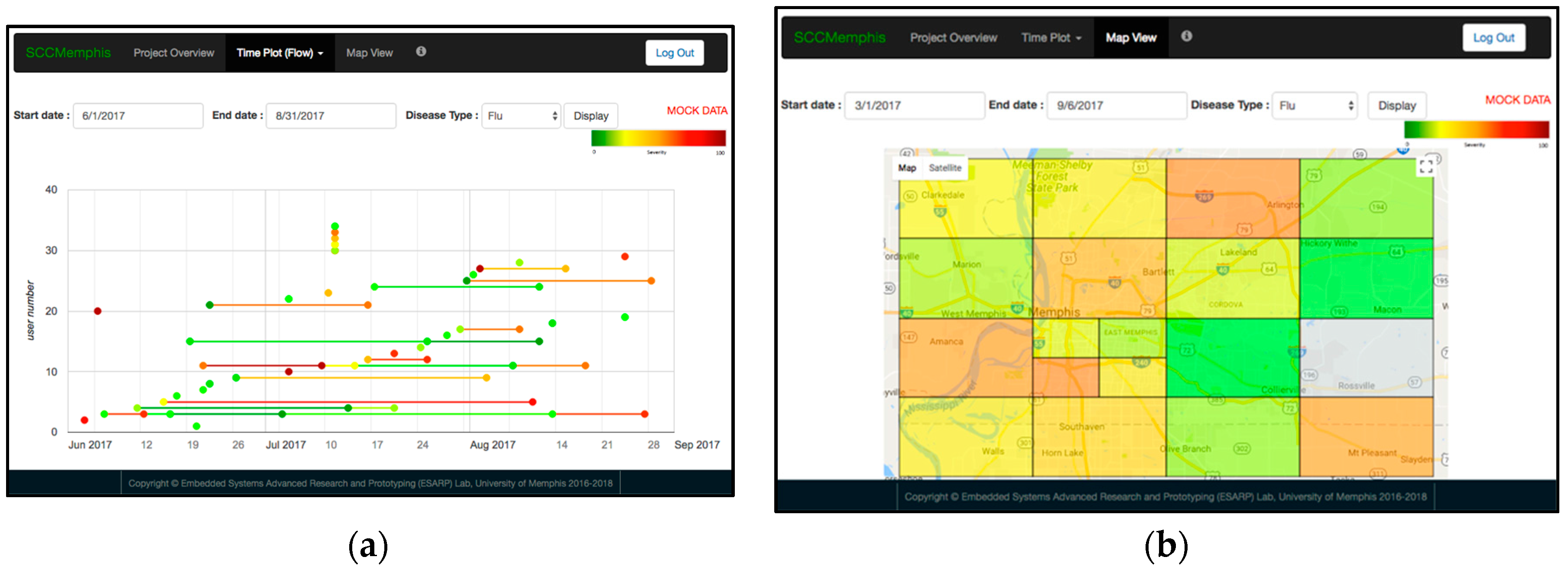
3.5. SCC Health Web-Server Test with Mock Data

Figure 18 shows spatial and temporal domain EoIs, where both plots represent severity in terms of color-coding as shown. The spatial plot (Map view) is overlaid on Google map that give a visual of disease distribution in various regions. Arbitrarily, we have selected a square grid format with smaller dimensions in densely populated areas (e.g., Memphis downtown). This severity color-coded plot can help identify specific regions needing more attention from public health and community organizations for disease specific targeted improvement of that portion of the community.

4. Discussions and Future Plan

Currently we are in the process of designing and testing other WRAP sensors, such as respiration sensors, heart rate sensors, and ECG sensors. All of these sensors use the same theory as discussed, but vary with transducer type, response nature, and sensor circuit design. All sensors will be prototyped on paper substrate and will be used as disposable body-worn patch electronic sensors. The scanner design is also being enhanced with the incorporation of an LCD display for ease of user interaction, battery charge status, and DC charging port for LiPo battery. A 3D printed packaging is also being developed to house the portable scanner. Algorithms for a few other diseases such as obstructive sleep apnea (OSA), chronic obstructive pulmonary disease (COPD), and arrhythmia are being developed as well.
The pilot study will include pre- and post-surveys to assess acceptability, wearability, usability, and related concerns. Before beginning the study, participants answer 11 questions assessing overall perceived health, education, experience monitoring their health, and experience with research. In addition, participants are asked about their familiarity and level of comfort with technology, expectations related to the technology used in the study, and level of comfort with sharing physiological data with individuals such as their medical doctor as well as on an anonymous website (such as SCC Health webserver). At the end of the 30-day study period, participants will answer 13 questions assessing any changes in their health status, whether pre-study expectations were met, their use of the study components, their level of comfort with using study components, and problems they may have experienced.
Recruitment of participants into the study (n = 12) uses partnerships with United Methodist Churches (UMC) in the greater Memphis, TN area. Meetings with men and women’s UMC groups along with outreach to individual UMC pastors and churches are being used to share information about the study and recruit potential participants.

5. Conclusions

IJP was utilized to fabricate completely functional WARP temperature sensor (Type D) circuits for physiological signal monitoring. The ability to develop thin film circuits on flexible substrates coupled with the simplicity of the WRAP sensors provides the wear-and-forget type body-worn sensors to monitor physiological signals. The WRAP sensors enjoy battery-less operation, thin and flexible prototyping, low component count, fast response time, and low RF power requirement and are particularly suitable for IJP technology. The prototypes were developed on flexible paper substrates as low-cost body-worn disposable electronic patches. The scanner probes these sensors wirelessly at 13.56 MHz using the inductive coupling principle, and the resistive transducer at the sensors modulates the amplitude of the reflected wave, which can be decoded with the envelope detector and subsequent circuitry. The data can be further analyzed by the smartphone app to compute severity (EoI). Anonymous sharing of these EoIs can be uploaded to the SCC Health webserver for knowledge gathering in both temporal and spatial domains. Self-monitoring of health also has broader implications including improvement of overall community health, and reduced hospital visits as well as the potential for substantial interaction by community members, thereby improving SCC community.

Acknowledgments

This material is based upon work supported by the National Science Foundation under Grant No. 1637250. This fund does not cover any cost of publication in open access.

Author Contributions

B.I.M. has developed the overall concept, oversee the project progress, manage the resources, developed the inkjet printed sensors, and wrote this paper; B.H. has contributed in community outreach, survey, and interaction with subjects; M.S.Z. has designed, prototyped, and tested the wearable scanner; M.J.R. has developed smartphone app, algorithms for severity computation, and tested the sensors with the scanner; S.A. has developed the webserver with spatial and temporal displays; and M.R. has provided disease related medical expertise.

Conflicts of Interest

The authors declare no conflict of interest. The funding sponsors had no role in the design of the study; in the collection, analyses, or interpretation of data; in the writing of the manuscript, and in the decision to publish the results.

References

  1. Riley, W.T.; Rivera, D.E.; Atienza, A.A.; Nilsen, W.; Allison, S.M.; Mermelstein, R. Health behavior models in the age of mobile interventions: Are our theories up to the task? Transl. Behav. Med. 2011, 1, 53–71. [Google Scholar] [CrossRef] [PubMed]
  2. Lazar, A.; Koehler, C.; Tanenbaum, J.; Nguyen, D.H. Why We Use and Abandon Smart Devices. In Proceedings of the ACM International Conference Pervasive and Ubiquitous Computing, Osaka, Japan, 7–11 September 2015; pp. 635–646. [Google Scholar]
  3. High Confidence Software and Systems Coordinating Group. Networking and Information Technology Research and Development Program. High-Confidence Medical Devices: Cyber-Physical Systems for 21st Century Health Care. Available online: http://www.nitrd.gov/About/MedDevice-FINAL1-web.pdf (accessed on 5 November 2017).
  4. Hu, L.; Wu, H.; Mantia, F.L.; Yang, Y.; Cui, Y. Thin, flexible secondary Li-Ion paper batteries. ACS Nano 2010, 4, 5843–5848. [Google Scholar] [CrossRef] [PubMed]
  5. Beeby, S.; White, N. Energy Harvesting for Autonomous Systems; Artech House: Norwood, MA, USA, 2014. [Google Scholar]
  6. Zhang, Y.; Zhang, F.; Shakhsheer, Y.; Silver, J.D.; Klinefelter, A.; Nagaraju, M.; Boley, J.; Pandey, J.; Shrivastava, A.; Carlson, E.J.; et al. A batteryless 19 μW MICS/ISM-band energy harvesting body sensor node SoC for ExG applications. IEEE J. Solid-State Circuits 2013, 48, 199–213. [Google Scholar] [CrossRef]
  7. Islam, S.K.; Fathy, A.; Wang, Y.; Kuhn, M.; Mahfouz, M. Hastle-free vitals. IEEE Microw. Mag. 2014, 15, S25–S33. [Google Scholar] [CrossRef]
  8. Occhiuzzi, C.; Caizzone, S.; Marrocco, G. Wireless sensing of things by passive RFID technology. IEEE Trans. Antenna Propag. 2012. Available online: https://iris.unipa.it/retrieve/handle/10447/100765/135912/10-Review.pdf (access on 5 November 2017).
  9. Yeager, D.J.; Powledge, P.S.; Prasad, R.; Wetherall, D.; Smith, J.R. Wirelessly-charged UHF tags for sensor data collection. In Proceedings of the 2008 IEEE International Conference on RFID, Las Vegas, NV, USA, 16–17 April 2008; pp. 320–327. [Google Scholar]
  10. Want, R. An Introduction to RFID Technology. IEEE Pervas. Comput. 2006, 5, 25–33. [Google Scholar] [CrossRef]
  11. Bae, J.; Song, K.; Lee, H.; Cho, H.; Yoo, H. A low-energy crystal-less double-FSK sensor node transceiver for wireless body-area network. IEEE J. Solid-State Circuits 2012, 47, 2678–2692. [Google Scholar] [CrossRef]
  12. Finkenzeller, K. The RFID Handbook: Fundamentals and Applications in Contactless Smart Cards and Identification; John Wiley and Sons: Hoboken, NJ, USA, 2003. [Google Scholar]
  13. Sawan, M.; Hu, Y.; Coulombe, J. Wireless smart implants dedicated to multichannel monitoring and microstimulation. IEEE Circuits Syst. Mag. 2005, 5, 21–39. [Google Scholar] [CrossRef]
  14. Bashirullah, R. Wireless implants. IEEE Microw. Mag. 2010, 11, S14–S23. [Google Scholar] [CrossRef]
  15. Thomas, S.J.; Besnoff, J.S.; Reynolds, M.S. Modulated backscatter for ultra-low power uplinks from wearable and implantable devices. In Proceedings of the 2012 ACM Workshop on Medical Communication Systems, New York, NY, USA, 13 August 2012; pp. 1–6. [Google Scholar]
  16. Nikitin, P.V.; Rao, K.V.S. Theory and measurement of backscattering from RFID tags. IEEE Antennas Propag. Mag. 2006, 48, 212–218. [Google Scholar] [CrossRef]
  17. Mamalis, B.; Gavalas, D.; Konstantopoulos, C.; Pantziou, G. Clustering in wireless sensor networks. In RFID and Sensor Networks: Architectures, Protocols, Security, and Integrations, 1st ed.; Zhang, Y., Ed.; CRC Press: Boca Raton, FL, USA, 2009; Chapter 12; pp. 323–353. [Google Scholar]
  18. Dementyev, A.; Smith, J.R. A wearable UHF RFID-based EEG system. In Proceedings of the 2013 IEEE International Conference on RFID, Penang, Malaysia, 30 April–2 May 2013; pp. 1–7. [Google Scholar]
  19. Wise, K.D.; Anderson, D.J.; Hetke, J.F.; Kipke, D.R.; Najafi, K. Wireless implantable microsystems: High-density electronic interfaces to the nervous system. Proc. IEEE 2004, 92, 76–97. [Google Scholar] [CrossRef]
  20. Wickamasinghe, A.; Ranasinghe, D.C.; Sample, A.P. Windware: Supporting ubiquitous computing with passive sensor enabled RFID. In Proceedings of the 2014 IEEE International Conference on RFID, Orlando, FL, USA, 8–10 April 2014; pp. 31–38. [Google Scholar]
  21. Robinson, E.J.H.; Smith, F.D.; Sullivan, K.M.E.; Franks, N.R. Do ants make direct comparisons? Proc. R. Soc. B 2009, 276, 2635–2641. [Google Scholar] [CrossRef] [PubMed]
  22. Poh, M.; Swenson, N.C.; Picard, R.W. A wearable sensor for unobtrusive, long-term assessment of electrodermal activity. IEEE Trans. Biomed. Eng. 2010, 57, 1243–1252. [Google Scholar] [PubMed]
  23. Popovic, Z.; Falkenstein, E.A.; Costinett, D.; Zane, R. Low-power far-field wireless powering for wireless sensors. Proc. IEEE 2013, 101, 1397–1409. [Google Scholar] [CrossRef]
  24. Falkenstein, E.; Costinett, D.; Zane, R.; Popovic, Z. Far-field RF-powered variable duty cycle wireless sensor platform. IEEE Trans. Circuits Syst. II Express Briefs 2011, 58, 822–826. [Google Scholar] [CrossRef]
  25. Mollazedeh, M.; Murrari, K.; Cauwenberghs, G.; Thakor, N.V. Wireless micropower instrumentation for multimodal acquisition of electrical and chemical neural activity. IEEE Trans. Biomed. Circuits Syst. 2009, 3, 388–397. [Google Scholar] [CrossRef] [PubMed]
  26. Yoo, J.; Yan, L.; Lee, S.; Kim, Y.; Yoo, H. A 5.2 mW self-configured wearable body sensor network controller and a 12 μW wirelessly powered sensor for a continuous health monitoring system. IEEE J. Solid-State Circuits 2010, 45, 178–188. [Google Scholar] [CrossRef]
  27. Towe, B.C. Passive Backscatter Biotelemetry for Neural Interfacing. In Proceedings of the 3rd International IEEE/EMBS Conference on Neural Engineering, Kohala Coast, HI, USA, 2–5 May 2007; pp. 144–147. [Google Scholar]
  28. Towe, B.C. Systems and Methods for Wireless Transmission of Biopotentials. U.S. Patent 2010/0198039 A1, 5 August 2010. [Google Scholar]
  29. Baldwin, H.A.; Depp, S.W.; Koelle, A.R.; Freyman, R.W. Interrogation, and Detection System. U.S. Patent 4075632, 21 February 1978. [Google Scholar]
  30. Schwerdt, H.N.; Xu, W.; Shekhar, S.; Abbaspour-Tamijani, A.; Towe, B.C.; Miranda, F.A.; Chae, J. A fully-pasive wireless microsystem for recording of neuropotentials using RF backscattering methods. J. Microelectromech. Syst. 2011, 20, 1119–1130. [Google Scholar] [CrossRef] [PubMed]
  31. Schwerdt, H.N.; Miranda, F.A.; Chae, J. Analysis of electromagnetic fields induced in operation of a wireless fully passive backscattering neurorecording microsystems in emulated human head tissue. IEEE Trans. Microw. Theory Tech. 2013, 61, 2170–2176. [Google Scholar] [CrossRef]
  32. Schwerdt, H.N.; Chae, J.; Miranda, F.A. Wireless performance of a fully passive neurorecording microsystem embedded in dispersive human head phantom. In Proceedings of the IEEE International Symposium on Antennas and Propagation, Chicago, IL, USA, 9 July 2012; pp. 1–2. [Google Scholar]
  33. Riistama, J.; Aittokallio, E.; Verho, J.; Lekkala, J. Totally passive wireless biopotential measurement sensor by utilizing inductively coupled resonance circuits. Sens. Actuators A 2010, 157, 313–321. [Google Scholar] [CrossRef]
  34. Luo, W.; Fu, Q.; Deng, J.; Yan, G.; Zhou, D.; Gong, S.; Hu, Y. An integrated passive impedance loaded SAW sensor. Sens. Actuators B Chem. 2013, 187, 215–220. [Google Scholar] [CrossRef]
  35. Karilainen, A.; Finnberg, T.; Uelzen, T.; Dembowski, K.; Månuller, J. Mobile Patient Monitoring Based on Impedance-Loaded SAW-Sensors. IEEE Trans. Ultrason. Ferroelectr. Freq. Control 2004, 51, 1464–1469. [Google Scholar] [CrossRef] [PubMed]
  36. Ferguson, J.E.; Redish, A.D. Wireless communication with implanted medical devices using the conductive properties of the body. Expert Rev. Med. Devices 2011, 8, 427–433. [Google Scholar] [CrossRef] [PubMed]
  37. Consul-Pacareu, S.; Arellano, D.; Morshed, B.I. Body-worn Fully-Passive Wireless Analog Sensors for Physiological Signal Capture through Load Modulation using Resistive Transducers. In Proceedings of the 2014 IEEE Healthcare Innovation and Point-of-Care Technologies Conference, Seattle, WA, USA, 8–10 October 2014; pp. 67–70. [Google Scholar]
  38. Consul-Pacareu, S.; Arellano, D.; Morshed, B.I. Body-worn Fully-Passive Wireless Analog Sensors for Biopotential Measurement through Load Modulation. In Proceedings of the 2015 IEEE Topical Conference on Biomedical Wireless Technologies, Networks, and Sensing Systems (BioWireleSS), San Diego, CA, USA, 25–28 January 2015; pp. 1–3. [Google Scholar]
  39. Morshed, B.I. Impedance Phlebography Based Pulse Sensing Using Inductively-Coupled Inkjet-Printed WRAP Sensor. In Proceedings of the Invited Paper, Commission B (Special Session: Wearable Antennas and Electronics), National Radio Science Meeting, Boulder, CO, USA, 4–6 January 2017. [Google Scholar]
  40. Patel, S.; Park, H.; Bonato, P.; Chan, L.; Rodgers, M. A review of wearable sensors and systems with application in rehabilitation. J. Neuroeng. Rehabil. 2012, 9, 1–17. [Google Scholar] [CrossRef] [PubMed] [Green Version]
  41. Zheng, Y.L.; Ding, X.R.; Poon, C.C.Y.; Lo, B.P.L.; Zhang, H.; Zhou, X.L.; Yang, G.Z.; Zhao, N.; Zhang, Y.T. Unobtrusive Sensing and Wearable Devices for Health Informatics. IEEE Trans. Biomed. Eng. 2014, 61, 1538–1554. [Google Scholar] [CrossRef] [PubMed]
  42. Frey, H.; Khan, H.R. Handbook of Thin Film Technology; Springer: Berlin/Heidelberg, Germany, 2015. [Google Scholar]
  43. Van Osch, T.H.J.; Percelaer, J.; de Laat, A.W.M.; Schubert, U.S. Inkjet printing of narrow conductive tracks on untreated polymeric substrates. Adv. Mater. 2008, 20, 343–345. [Google Scholar] [CrossRef]
  44. Niittynen, J.; Sowade, E.; Kang, H.; Baumann, R.R.; Mäntysalo, M. Comparison of laser and intense pulse light sintering (IPL) for inkjet-printed copper nanoparticle layers. Nat. Sci. Rep. 2015, 5, 8832. [Google Scholar] [CrossRef] [PubMed]
  45. Shaker, G.; Safavi-Naeini, S.; Sangary, N.; Tentzeris, M.M. Inkjet printing of ultrawideband (UWB) antennas on paper-based substrates. IEEE Antennas Wirel. Propag. Lett. 2011, 10, 111–114. [Google Scholar] [CrossRef]
  46. Cook, B.S.; Cooper, J.R.; Tentzeris, M.M. Multi-layer RF Capacitors on Flexible Substrates Utilizing Inkjet Printed Dielectric Polymers. IEEE Microw. Wirel. Compon. Lett. 2013, 23, 353–355. [Google Scholar] [CrossRef]
  47. Kung, B.J.; Lee, C.K.; Oh, J.H. All-inkjet-printed electrical components and circuit fabrication on a plastic substrate. Microelectron. Eng. 2012, 97, 251–254. [Google Scholar] [CrossRef]
  48. McKerrcher, G.; Perez, J.G.; Shamim, A. Fully Inkjet Printed RF Inductors and Capacitors Using Polymer Dielectric and Silver Conductive Ink with through Vias. IEEE Trans. Electron. Devices 2015, 62, 1002–1009. [Google Scholar] [CrossRef]
  49. Kim, D.H.; Lu, N.; Ma, R.; Kim, Y.S.; Kim, R.H.; Wang, S.; Wu, J.; Won, S.M.; Tao, H.; Islam, A.; et al. Epidermal electronics. Science 2011, 333, 838–843. [Google Scholar] [CrossRef] [PubMed]
  50. Xu, S.; Zhang, Y.; Jia, L.; Mathewson, K.E.; Jang, K.I.; Kim, J.; Fu, H.; Huang, X.; Chava, P.; Wang, R.; et al. Soft microfluidic assemblies of sensors, circuits, and radios for the skin. Science 2014, 344, 70–74. [Google Scholar] [CrossRef] [PubMed]
  51. Kim, D.; Ghaffari, R.; Lu, N.; Rogers, J.A. Flexible and stretchable electronics for biointegrated devices. Annu. Rev. Biomed. Eng. 2012, 14, 113–128. [Google Scholar] [CrossRef] [PubMed]
  52. Noroozi, B.; Morshed, B.I. PSC Optimization of 13.56-MHz Resistive Wireless Analog Passive Sensors. IEEE Trans. Microw. Theory Tech. 2017, 65, 3548–3555. [Google Scholar] [CrossRef]
  53. Morshed, B.I. Dual Coil for Remote Probing of Signals using Resistive Wireless Analog Passive Sensors (rWAPS). In Proceedings of the Invited Paper, Commission B, National Radio Science Meeting, Boulder, CO, USA, 6–9 January 2016. [Google Scholar]
  54. Noroozi, B.; Morshed, B.I. Formal Method for PSC Design Optimization of 13.56 MHz Resistive Wireless Analog Passive Sensors (rWAPS). Presented at the IEEE Radio and Wireless Week Conference, Austin, TX, USA, 24–27 January 2016. [Google Scholar]
Figure 1. A conceptual diagram depicting the overall system framework.
Jlpea 07 00026 g001
Figure 2. Wireless Resistive Analog Passive (WRAP) temperature sensor (a) schematic; (b) layout design; (c) inkjet printed layout on a paper substrate (13 cm length); and (d) component populated using silver epoxy for a fully functional sensor.
Jlpea 07 00026 g002
Figure 3. (a) The relationship of drop-spacing and drop size for inkjet printing (IJP) traces; (b) a cross-sectional drawing of the additive manufacturing process of the WRAP sensors (not to scale).
Jlpea 07 00026 g003
Figure 4. Functional block diagram of the wearable scanner device.
Jlpea 07 00026 g004
Figure 5. Schematic diagram of the analog circuit portion of the scanner. (a) The RF driver circuit of the scanner coil; (b) the envelope detector and signal processing circuit.
Jlpea 07 00026 g005
Figure 6. Firmware sequence diagram of the wearable scanner device.
Jlpea 07 00026 g006
Figure 7. Sequence diagram of the interfaces of the custom smartphone app.
Jlpea 07 00026 g007
Figure 8. Smart and Connected Communities (SCC) Health web-server interaction diagram.
Jlpea 07 00026 g008
Figure 9. (a) An optical microscope image of the coil section of the printed sensor; (b) magnified image shows smooth edges of IJP traces when printed along the direction of the printing and rugged edges when printed perpendicular to the direction of the printing.
Jlpea 07 00026 g009
Figure 10. (a) An optical microscope photograph of the silver epoxy connection of a discrete component on the printed Ag traces on paper; (b) SEM image showing a cross-sectional view of the printed silver trace on a paper substrate.
Jlpea 07 00026 g010
Figure 11. IJP Ag trace printing issues: (a) Micro-gap on traces resulting discontinuity; (b) misfired droplets due to partially blocked nozzles; and (c) rugged edges of a printed traces.
Jlpea 07 00026 g011
Figure 12. Experimental setup for data collection of a WRAP temperature senor using a scanner board. The controllable temperature heat pad is attached on the table under the sensor. (Inset) WRAP temperature sensor printed on paper can be easily flexed.
Jlpea 07 00026 g012
Figure 13. WRAP temperature sensor response captured by an oscilloscope for various stages of the signal during a burst applied to capture data from the sensor: (top) Carrier signal at the scanner coil, (middle) signal at the envelope detector, and (bottom) signal at the input of the ADC.
Jlpea 07 00026 g013
Figure 14. Received data of WRAP temperature sensor collected at the smartphone app for various temperatures depicting change of RC delay corresponding to the temperature.
Jlpea 07 00026 g014
Figure 15. Experimental functional verification of WRAP temperature sensor.
Jlpea 07 00026 g015
Figure 16. Captured delays for a various temperatures with fixed co-axial separation of the scanner and the WRAP temperature sensor coils.
Jlpea 07 00026 g016
Figure 17. Snapshots of various graphical user interfaces (GUI) of the custom smartphone app. Top-row left to right: Login screen, Main menu, Settings menu, Admin login screen, and Bluetooth setup menu. Bottom-row left to right: Diagnostics menu, One stop service menu, Sensor data collection menu, Severity (EoI) computation page, and Display of a temperature severity (EoI).
Jlpea 07 00026 g017
Figure 18. Temporal flow (a) and spatial (b) plots of EoI mock data at SCC Health web-server.
Jlpea 07 00026 g018
Table 1. Flu severity (Events-of-Interest [EoI]) assignment based on core-body temperature.
Temp. (°F)SeveritySuggestive PromptEoI RatingColor Code for EoI Ranking
97NormalNormal0Dark green
98NormalNormal0.1Green
99NormalNormal0.2Light green
100Low grade feverLow fever, Consider consulting your doctor0.3Green-yellow
101Low grade feverLow fever, Consider consulting your doctor0.4Yellow
102Intermediate feverMedium fever, consult your doctor0.5Yellow-orange
103High grade feverHigh fever, consult your doctor0.6Orange
104High grade feverHigh fever, consult your doctor0.7Orange-red
105Extreme feverVery high fever, consult your doctor immediately0.8Red
106Extreme feverVery high fever, consult your doctor immediately0.9Dark red
107Medical emergencyExtremely high fever, consult your doctor immediately1.0Dark red-Maroon
Table 2. Measured resistances of printed traces among various pads of WRAP temperature sensors.
Jlpea 07 00026 i001
PadsR (Ω)PadsR (Ω)PadsR (Ω)PadsR (Ω)PadsR (Ω)PadsR (Ω)
A-B13.3A-D13.4E-F0.1H-I2.3K-L0.2N-O0.1
A-C13.2B-D0.3E-G2.6H-J2.6K-M0.3P-Q0.1
B-C0.9C-D1.0F-G2.6I-J0.4L-M0.1
Table 3. Power consumption of various blocks of the wearable scanner device.
Scanner DevicePower Consumption
Microcontroller board with DDS on94.5 mW
Microcontroller board with DDS off72.9 mW
Analog amplifier406 mW

