Forwarding Path Limitation and Instruction Allocation for In-Order Processor with ALU Cascading

1
Department of Computer Science, Faculty of Informatics, Kogakuin University, 1-24-2 Nishi-shinjuku, Shinjuku-ku, Tokyo 163-8677, Japan
2
Department of Computer Science and Engineering, Toyohashi University of Technology, 1-1 Hibarigaoka Tenpaku-cho, Toyohashi-shi, Aichi-ken 441-8580, Japan
3
Advanced Networking Division, Information Technology Center, Nagoya University, Furo-cho, Chikusa-ku, Nagoya-shi, Aichi-ken 464-8601, Japan
*
Author to whom correspondence should be addressed.
J. Low Power Electron. Appl. 2017, 7(4), 32; https://doi.org/10.3390/jlpea7040032
Submission received: 6 November 2017
/
Revised: 5 December 2017
/
Accepted: 12 December 2017
/
Published: 14 December 2017
Abstract
:Much research focuses on many-core processors, which possess a vast number of cores. Their area, energy consumption, and performance have a tendency to be proportional to the number of cores. It is better to utilize in-order (IO) execution for better area/energy efficiency. However, expanding two-way IO to three-way IO offers very little improvement, since data dependency limits the effectiveness. In addition, if the core is changed from IO to out-of-order (OoO) execution to improve Instruction Per Cycle(IPC), area and energy consumption increases significantly. The combination of IO execution and Arithmetic Logic Unit(ALU) cascading is an effective solution to alleviate this problem. However, ALU cascading is implemented by complex bypass circuits because it requires a connection between all outputs and all inputs of all ALUs. The hardware complexity of the bypass circuits increases area, energy consumption, and delay. In this study, we proposed a mechanism that limits the number of the forwarding paths and allocates instructions to ALUs in accordance with the limited paths. This mechanism scales down bypass circuits to reduce the hardware complexity. Our evaluation results show that our proposed mechanism can reduce the area by 38.7%, the energy by 41.1%, and the delay by 23.2% with very little IPC loss on average, as compared with the conventional mechanism.
1. Introduction
Until recently, increases in clock frequency have raised the processing speed of processors. However, this method has reached its improvement limit. In addition, energy consumption has grown in proportion as the processing speed rises. Today, much research focuses on many-core processors, which have a vast number of cores inside. Their area and energy consumption have a tendency to be proportional to the number of cores.
It is better to utilize in-order (IO) execution for its good area/energy efficiency compared to out-of-order (OoO) execution. IO execution is a method that executes instructions in program order. If the execution width of the processor is two-way, the processor executes two instructions per single clock cycle. If two consecutive instructions are not data-dependent, it is possible to execute them in one cycle. If not, the dependency source instruction (denoted as “producer”) is executed in a cycle, and then the dependency destination instruction (denoted as “consumer”) is executed in the subsequent cycle.
The one-way or two-way IO processor is used as a core for the many-core processor and is often used for a high-end embedded system. It might seem to be a solution for further performance to expand two-way IO to three-way. However, three-way IO execution offers little improvement, since data dependency limits the effectiveness.
The out-of-order execution can overcome this limitation. This method executes instructions out of program order when they are ready in the pool of instructions which are provided in program order. Therefore, the OoO execution can considerably increase the number of executable instructions per cycle to improve the IPC compared with IO execution. The examples for OoO core are Intel Atom [1] and ARM Cortex-A15 [2]. However, this method increases area and energy significantly.
To alleviate this problem, in previous work [3], we proposed to adopt the combination of IO execution and ALU cascading and we confirmed that a three-way IO core with ALU cascading gives better performance than a two-way OoO core because of the combination and the shorter pipeline stages which was enabled by the IO execution.
ALU cascading is a technique that forwards the result of a producer to one or more consumers via bypass circuits that connect the output of an ALU to the inputs of other ALUs. It is able to execute a producer and one or more consumers in one cycle if the producer is executed in the first half of the clock and the consumers are executed in the latter half. Unfortunately, ALU cascading is implemented by complex bypass circuits because it requires a connection between all outputs and all inputs of all ALUs. The hardware complexity of the bypass circuits increases area, energy, and delay.
In this paper, we focus on the low utilization efficiency of the forwarding paths provided by the bypass circuits. To reduce hardware complexity, we propose a novel ALU cascading mechanism, which limits the number of the forwarding paths and allocates instructions to ALUs in accordance with the limited paths. (The work [4] is an interim report of the study tackled in this paper. This paper brings the interim report to completion by reconstructing all the descriptions and developing the contents.)
2. ALU Cascading
While higher performance is required, the most recent processors are face and have to deal with the problems of excess energy consumption and heat generation for longer battery life and lower cooling costs. We focus on the Dynamic Voltage and Frequency Scaling (DVFS) as one of the solutions for these restrictions. DVFS reduces clock frequency and power supply voltage according to reduction in the processor load. Some latest processors can operate with such a low supply voltage of less than one volt. However, different from the frequency, the variation range of the supply voltage is relatively very narrow. Therefore, when the frequency is lower than some point, the processor cannot degrade the power supply voltage due to the narrow variable range, but can degrade the frequency. Consequently, idle time occurs after the execution of the producer on an ALU in the clock cycle. If the idle time is sufficiently long, ALU cascading allows another ALU to execute the consumer.
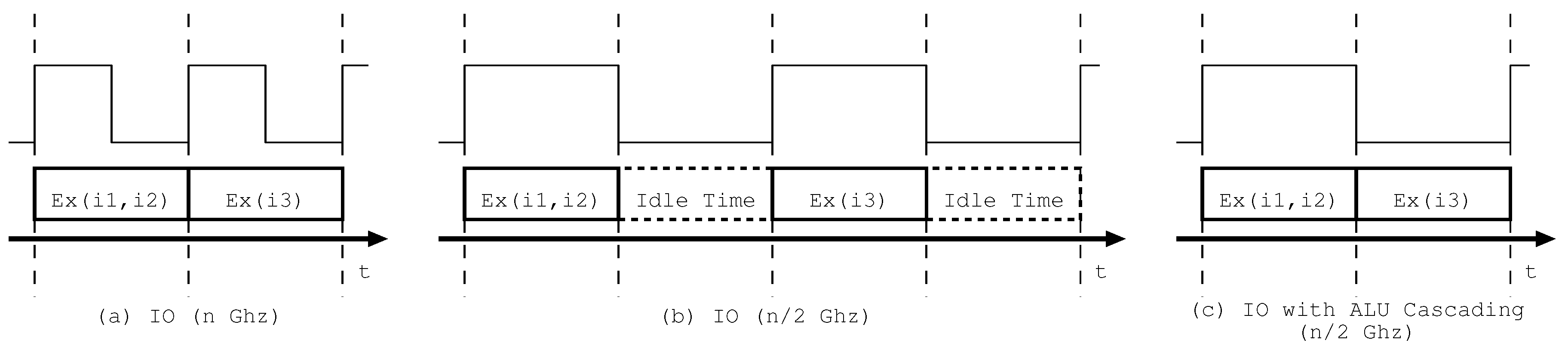
We illustrate the details of ALU cascading by assuming a three-way IO processor. Figure 1a–c shows the operation timings of instructions on ALUs at the different frequencies. We use instructions i1, i2, and i3: i1 and i3 are data dependent and i2 is data independent. Figure 1a shows the operation timing of i1–i3 when the operation time is the same as the clock cycle time and the supply voltage reaches the lower limit. The producer i1 and the data-independent i2 are executed in the first cycle, and then consumer i3 is executed in the second cycle, where “Ex(ix,iy)” means that instruction ix and iy are executed on ALUs.
Figure 1b,c shows the operation timings with and without ALU cascading when the frequency is reduced to half with maintaining the same voltage due to half the processor load and the lower limit of the supply voltage. The operation time of each instruction does not change but the cycle time increases twofold. Therefore, in Figure 1b, idle time occurs in the second half of each clock cycle. On the other hand, in Figure 1c, all instructions are executed in the same cycle by using the ALU cascading, although i1 and i2 are executed in the first half of the clock and i3 is executed in the second half of the clock. The above indicates that ALU cascading improves the utilization efficiency of clock cycle time.
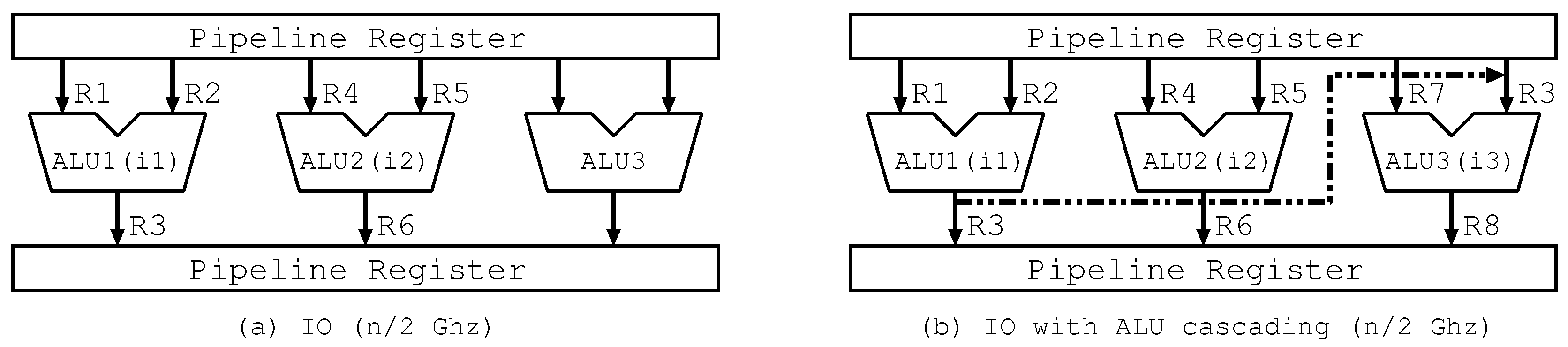
Figure 2a,b shows the executed instructions and the data flow of instructions on three ALUs with/without ALU cascading. In the figure, “ALUx (in)” means ALUx executing in. In Figure 2b, we depict only an actually used forwarding path to facilitate understanding. We use the same assumption as that in Figure 1. Besides, we determine the number of ALUs in accordance with the number of ways and show the source/destination register numbers of i1–i3 instead of actual register data in the figure. It should be noted that the destination register number of producer i1 is the same as the right side source register number of consumer i3. The operations in Figure 2a,b correspond to those in the first cycle in Figure 1b,c, respectively.
Figure 2a shows that i1 and i2 are executed on two ALUs in 1st cycle, while Figure 2b shows that i1–i3 are executed on three ALUs in the same cycle by forwarding the register data of R3 from i1 to i3 via the bypass circuits. The above clearly indicates that ALU cascading efficiently utilizes ALU resources.
The timing adopted in the proposed schemes is as follows. When the workload of the processor decreases, DVFS recedes clock frequency of the processor. Typical DVFS also reduces supply voltage in proportion to the clock frequency reduction. However, recently, due to process technology advancement, current processor operates with comparatively low supply voltage so that there’s less space to reduce supply voltage. In such case, the processor has to leave idle time after the clock frequency reduction as shown in transition from Figure 1a to Figure 1b. ALU cascading utilizes this idle time effectively by filling the idle time with execution of following data dependent instruction as shown in Figure 1c. The execution with ALU cascading is introduces in Figure 2. Assuming that there is data dependency between i1 and i3 through R3, Figure 2a shows execution without ALU cascading. The processor operates with in-order execution so that the processor cannot fill ALU3. On the other hand, as shown in Figure 2b, the processor can fill ALU3 with i3 by utilizing ALU cascading path between ALU1 and ALU3. In this case, i1 and i2 are executed in first half of the clock cycle, as shown in Figure 1c, then R3, the result of i1, is transferred to the input of ALU3. After that, i3 is executed in latter half of the clock cycle, as shown in Figure 1c with obtained R3.
The previous work [3] proposed using the combination of IO execution and ALU cascading rather than OoO execution from the view point of hardware simplicity. In addition, it performed the IPC evaluations of two models: x-way OoO model and x-way y-chain IO model, where x indicates the issue width, y means the max depth of a chain of forwarding paths. For example, in the three-way one-chain IO, if i1–i3 have sequential dependency, which means that i3 depends on i2 and i2 depends on i1, only i1 and i2 are issued because the max chain depth is 1. In the evaluation, the Simple Scalar Tool Set [5] and SPEC2000 benchmarks were used.
The evaluation results confirmed the following: (1) The appropriate chain depth is 1 for the three-way IO core with ALU cascading because three consecutive instructions rarely have the sequential data dependency. (2) The three-way one-chain IO core outperforms the two-way OoO core, which is used in such as Intel Atom core, because of the ALU cascading and smaller branch prediction miss penalty arising from the hardware simplicity of IO core. (3) The four-way one-chain IO core cannot exceed but is comparable with the three-way OoO core, which is used in such as ARM Cortex-A15 because of the same reason as described in (2). The above confirmations indicate that it is better to adopt the three- or four-way IO core with ALU cascading if we want to achieve high IPC without introducing the hardware complexity of an OoO core.
3. Related Work
There are some studies about adopting ALU cascading to the processors. The following are several studies about static ALU cascading adoption which are under the concept level. Sazeides et al. proved the performance potential of ALU cascading under SPARC V8 architecture [6]. The call ALU cascading is data collapsing and proves its potential under assuming ideal ALU cascading. Based on this concept, Kise et al. tried to achieve low power architecture by ALU cascading [7] and Meng et al. tried to improve IPC in superscalar processor [8]. As an abaxial use of ALU cascading, Watanabe et al. use ALU cascading to alleviate circuit delay variations from semiconductor process variations [9].
To adopt ALU cascading to under practical assumption, some dynamic ALU cascading adoption has been tried. Ozawa et al. tried to adopt ALU cascading to asynchronous superscalar processor [10,11]. The processor issues several instructions, which are fetched simultaneously, without considering data dependencies. To resolve the data dependency, the execution stage of the processor checks data dependence and connects an output of an ALU into an input of the other ALU. The cycle time of the execution stage is automatically extended because the processor is running under asynchronous operation.
Sasaki et al. propose ALU cascading relationship in decode stage and store it to instruction window of out-of-order processor [12]. In this way, they realized ALU cascading in synchronous out-of-order processor under low clock frequency. A similar instruction combining method is used for relaxing instruction scheduling [13,14]. Yao et al. propose dynamic ALU cascading scheduling in the instruction window of out-of-order processor [15]. They wake up cascading candidate instructions with two prior dependencies to issue both prior instruction and latter instruction in ALU cascading in the same clock cycle.
On the other hand, different from architecture level research above, some device level research has also been presented. Amrutur et al. evaluated some power efficient across a large range of computation loads on advanced process nodes with large process variations [16]. Lin et al. tried to implement DVS on algorithm and device level [17]. They designed and evaluated power saving scheduling algorithm for real-time systems in embedded system.
4. Our Proposed Approach
4.1. Principle
In the previous study, we proposed to apply ALU cascading to IO core that is relatively simple in the hardware complexity compared with OoO core, and reported that the proposal is effective and one-chain is sufficient for the proposal based on the IPC evaluation results.
However, ALU cascading has a problem in that the complex bypass circuits are required to connect the outputs and inputs of all ALUs for forwarding data between dependent instructions, although the previous study performed neither discussion nor proposal about concrete bypass circuits. The hardware complexity of them grows according to the number of ALUs, resulting in larger area, higher energy, and longer delay.
Figure 3 illustrates the forwarding paths in conventional ALU cascading, which is also called “Full Path” in this paper. In this figure, we assume a three-way core with three ALUs and use three instructions i1–i3: i3 depends on i1 and i2 does not depend on the others. To facilitate understanding of our principle, the figure omits the bypass circuits including wires and multiplexers and shows only the forwarding paths provided by the omitted ones. As shown in the figure, Full Path prepares all the possible forwarding paths that connect from the output of each ALU to the inputs of the other ALUs, scaling up the bypass circuits. However, the actually used paths are only one: the path from the ALU1 to the ALU3. This confirms that, even though most of the bypass circuits are not used for data forwarding in each cycle, they adversely affect area, energy, and delay.
Even if ALU cascading is applied, a Full Path model is required in in-order execution. For example, the forwarding path of ALU1-ALU2, ALU1-ALU3, and ALU2-ALU3 are not enough in Figure 3. A detailed example is as follows. Postulate that an instruction remains in the ALU3 of a three-way Full Path model, such as that shown in Figure 3, since it is not executed by data dependence and limitation of the number of data forwarding. In the next cycle, subsequent instructions are already filled in pipeline of ALU1 and ALU2 so that they are filled into ALU1 and ALU2. The instruction might have data dependence on the remaining instruction on ALU3. In this case, the execution result of the third ALU is forwarded to the previous ALUs. For the above reasons, forwarding paths need to be connected to previous ALUs.
IPC improvements are saturating even if a processor is expanded to greater than two-way. The IO execution normally adopts two-way since the data dependencies of instructions severely limit instruction level parallelism. There is rarely no data dependency between three consecutive instructions when an IO processor executes a program. This means that three or more ALUs do not concurrently operate. Therefore IPC enhancement is below 1% if the execution width is increased from two-way. To address this problem, in the previous study [3], we proposed the utilization of ALU cascading in the IO execution.
In this paper, we handle the problem of bypass circuits and propose a novel mechanism that reduces the hardware complexity of them by instruction allocation and forwarding path limitation. First, we focus on the low utilization efficiency of the forwarding paths shown in Figure 3. This is because the number of actual forwarding paths is strictly restricted by the issue width and the property of programs (the previous work reported that three-way IO core mostly needs at most one-chain depth of forwarding paths), while Full Path increases the possible forwarding paths according to the issue width. This obviously indicates that the increase in the issue width furthermore reduces path utilization efficiency. Therefore, to address the above problem, we propose to: (1) limit the forwarding paths to scale down the bypass circuits; and (2) allocate instructions to ALUs to perform the data forwarding on the limited ones.
Figure 4 illustrates the allocation paths and the forwarding paths in our proposed ALU cascading, which is also called “Lim Path” in this paper. In addition, we use the term “Lim Path(ALUx-y)”, which means the forwarding paths are limited to only the path from ALUx to ALUy. Therefore, the ALU cascading in the figure is called “Lim Path(ALU1-2)”.
Firstly, the allocation circuit performs the instruction allocation to change the placement of the instructions in order to perform the data forwarding on the limited ones. Although each instruction has various information—opcode, register numbers, register data, data dependency, etc.—the figure shows only register numbers (denoted as “rn”) and register data (denoted as “Rn”) on the paths to facilitate understanding of our principle in the figure.
Secondly, the register file is accessed by register numbers and register data are acquired. The register file has six read ports since the decode width is 3 and the number of source operands are 2. The length of register number is 5 bit and the length of register data is 64 bit. The above parameters except for decode width are determined by the Alpha ISA that we assume in this paper. The read ports of the register file are associated with the inputs of ALUs. For example, the register data from read port 1 is sent to the left side input of ALU1. Therefore, the instruction allocation can be performed before register file read.
Lastly, the producer i1 and the independent instruction i2 are executed on the ALU1 and ALU3, the result of i1 is forwarded to the left side input of ALU2, and then i3 is executed on ALU2.
The points in the figure are as follows. Our proposed mechanism limits the forwarding paths to only one: the path from the ALU1 to the ALU2, successfully scaling down the bypass circuits. Although the paths are limited, the allocation circuit appropriately allocates the instructions, enabling one-chain data forwarding. The allocation circuit is an additional cost. However, it can be suppressed since the volume of instruction information processed during the instruction allocation is smaller than that processed during the data forwarding.
4.2. Hardware Mechanism
The proposed mechanism includes the allocation circuit and the bypass circuits.
4.2.1. Allocation Circuit
The allocation circuit is a crossbar switch placed in front of the register file and it changes the instruction placement, which determines on which ALU each instruction is executed, according to the information relating limited paths and data dependency. The data dependence information is already used by the existing mechanisms such as multi-way in-order execution and the conventional ALU cascading. Therefore, we assume that the additional circuits are not required for generating the data dependence information, which is sent to the allocation circuit.
For a detailed explanation, we assume the following machine state: there are ALU1, ALU2, and ALU3; only the output of ALU1 is connected with the inputs of ALU2; and the instruction placement {i1, i2, and i3} is the input of the allocation circuit. In this state, the examples of data dependence and the instruction allocation are as follows.
- i2 depends on i1The placement is not changed: {i1, i2, and i3}.
- i3 depends on i1It is changed to {i1, i3, and i2}.
- i3 depends on i2It is changed to {i2, i3, and i1}.
- both i2 and i3 depend on i1The replacement is not changed. However, i3 is not issued since there is only one forwarding path.
- i3 depend on both i1 and i2The replacement is not changed. However, i3 is not issued because of the same reason as the above.
- i3 depend on i2 and i2 depends on i1The replacement is not changed. However, i3 is not issued because of the same reason as the above.
In this paper, we treat only one-chain forwarding. Therefore, more than two-chain forwarding is not performed such as the sixth example above. As shown in the first to fifth examples above, there are different patterns of one-chain: one producer and one consumer; one producer and n consumers (); and two producers and one consumer, where the max value of n is determined by the issue width while the max number of producers is two since the max number of source operands is two in the assumed ISA. However, there are a many number of patterns for the discussion. Therefore, in this paper, we choose the following patterns: (1) one producer and one consumer; and (2) one producer and two consumers (the evaluation results in Section 5 confirm that the chosen patterns achieve sufficiently high IPC).
It takes time for the allocation circuit to allocate instructions. However, we assume the delay of the allocation circuit does not affect the cycle time due to the following reason. The register file is accessed by the decoded and executed instructions. If the producer is executed and the consumer is decoded, the read/write operations of the same register can be performed in the same cycle. To process the operations correctly, the register data is written to the register file in the first half of the clock, and then it is read from there in the second half [18]. This implementation of the register file allows the allocation circuit to operate in parallel with the write operation. (If the delay of the allocation circuit is very large, it may exceed the time period of the first half of the clock, resulting in the adverse influence on the clock cycle. However, the evaluation results in Section 5 confirm that the delay of the allocation circuit is small.)
4.2.2. Bypass Circuits
This section describes the bypass circuits of both the conventional mechanism (Full Path) and our proposed mechanism (Lim Path). The parameters of the mechanisms are way, chain depth, and chain width, where chain width means the maximum number of chains. Since the number of combinations of parameters is too many, we choose a part of them for discussion. In addition, as already mentioned, the patterns of one-chain are limited to: (1) one producer and one consumer; and (2) one producer and two consumers.
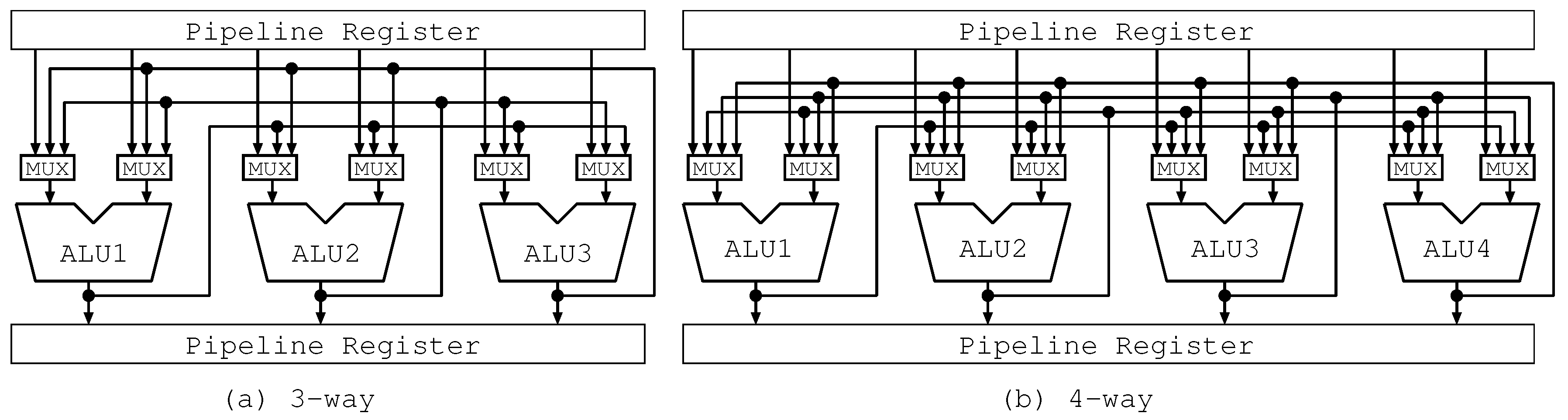
Firstly, we depict the cases of three-way in Figure 5a, Figure 6a and Figure 7a. Figure 5a shows the bypass circuits of the three-way Full Path. The bypass circuits connect the output of each ALU and the inputs of the other ones. They include the long wires corresponding to all the possible forwarding paths and six multiplexers with three inputs located at all the input sides of ALUs. Each multiplexer selects one among three inputs: an operand from the pipeline register and two operands forwarded from the other ALUs.
On the other hand, Figure 6a and Figure 7a show the bypass circuits of the three-way Lim Path(ALU1-2,ALU1-3) and the three-way Lim Path(ALU1-2), respectively. In Figure 6a, there is a long wire and 4 multiplexers with two inputs. Each multiplexer selects one among two inputs: an operand from the pipeline register and one forwarded from another ALU. In Figure 7a, the number of multiplexers is reduced to a half. It implies reducing the number of long wires and capacitive loads, resulting in good influence on clock frequency. As shown in these figures, our proposed mechanism reduces the complexity of bypass circuits.
Secondly, we represent the cases of four-way in Figure 5b, Figure 6b and Figure 7b. Figure 5b shows the bypass circuits of the four-way Full Path. This figure is similar to Figure 5a. However, according to the increase in way, the Full Path increases the scale of the bypass circuits: the number of wires; the number of multiplexers; and the input size of multiplexers.
On the other hand, Figure 6b and Figure 7b, which correspond to Figure 6a and Figure 7a, show the bypass circuits of the four-way Lim Path(ALU1-2,ALU1-3) and the four-way Lim Path(ALU1-2,ALU3-4), respectively. In Figure 6b, the bypass circuits are the same as those in Figure 6a. In Figure 7b, there are two one-chain forwarding paths. Each of them is the same as that in Figure 7a. Similar to the three-way Lim Path, four-way Lim Path reduces the scale of the bypass circuits more than four-way Full Path.
Bypass circuits consists of plural multiplexer which chooses one output between two inputs. On the other hand, allocation circuit is single crossbar switch which choose plural outputs from plural inputs. The circuit receives an instruction allocation information and data of instructions which is executed at appropriate ALU in next cycle. Then, the circuit allocates instruction data to each output based on allocation information.
5. Evaluation
5.1. Evaluation Environment
To confirm the positive and negative impacts of our mechanism, we evaluate the conventional and our proposed mechanisms. The evaluation items are as follows.
- Area
- Energy
- Delay
- Instructions Per Cycle (IPC) of the core
The area, energy, and delay were evaluated as follows. Firstly, we wrote the mechanisms in Verilog HDL. Secondly, we used Synopsys Design Compiler to perform logic synthesis on them. At this point, the results of area and delay were obtained. Lastly, we used Synopsys Prime Time to acquire energy measurement. The above evaluations used the standard-cell library for the Rohm 180-nm process. This process is still currently used for low commercial power LSI, although it is an old one because it does not require complicated manufacture process until packaging. The discussion of our research is based on such a field. In addition, this process could be used for chip trial production of Rohm Co., Ltd. (Kyoto Prefecture, Japan).
The IPC was evaluated as explained below. We used the revised processor simulator in the Simple Scalar Tool Set [5] and the SPEC2000 and SPEC2006 benchmarks. Each benchmark program includes the initialization phase. Therefore, firstly, 2 billion instructions were skipped. Secondly, 500 million instructions were executed for the evaluation.
Table 1 shows the processor configuration. The first four parameters were used for the evaluation of area, energy, and delay. Among them, the first two are commonly used for Full Path and Lim Path and the rest are used only for Lim Path. In the cases of three- and four-way Lim Paths, we used the patterns of one-chain forwarding shown in Figure 6a,b and Figure 7a,b. The chain depth in the Full Path model is limited to one based on the result of previous work [3] which is described in end of Section 2.
All the parameters are used for evaluating the IPC. They determine the configuration of the processors with the conventional and our proposed mechanisms. In the table, the variable n is common for the fetch, decode, issue, and commit widths and the number of integer ALUs (denoted as “iALUs”). In addition, n is the same as the execution width, which is 3 or 4.
5.2. Area, Energy, and Delay
As mentioned in Section 5.1, area and delay results are obtained when Synopsys Design Compiler performs logic synthesis. On the other hand, power results are obtained by running Synopsys Prime Time. The power related synthesis parameters are as follows.
- Operating Conditions: typical323
- Wire Load Model Mode: top324
- Global Operating Voltage: 1.8325
- Load for all outputs: 0.02315043326
Compared with Full Path, Lim Path has a good influence on the area, the energy, and the delay due to the limitation of the forwarding paths.
Figure 8, Figure 9 and Figure 10 show the area, the energy consumption, and the delay, respectively, of the Full Path and Lim Path. As noted before, we varied the number of ways from two to three and the combinations of bypass circuits. The above results are obtained by evaluating both the allocation circuit and the bypass circuits which construct Lim Path.
In Figure 8, the horizontal axis shows the number of ways. The vertical axis indicates the area. Each group of several bars represents the normalized area for different combinations of forwarding paths. In each group, the area of Lim Path is normalized by that of Full Path with the same way. Therefore, the area of Full Path is always 100%. Each bar of Lim Path has two parts: a “Allocation” part and a “Bypass” part, which, respectively, indicate the energy of the allocation circuit and that of the bypass circuits.
Figure 8, Figure 9 and Figure 10 are the same figures, excluding that their axes indicate different evaluation items, and only in Figure 10, a “Allocation” part is separated from the upper side on a “Bypass” part. (The bypass circuit and the allocation circuit operate in the different stages. In addition, the operation timings of them do not interfere with each other.)
Figure 8 and Figure 9 confirm that Lim Path reduces the area and the energy consumption in comparison with Full Path. The Lim Path scales down bypass circuits, decreasing the area and the energy. On the other hand, it requires the allocation circuit which is an extra cost, increasing the area and the energy. However, the hardware cost reduction of Lim Path by shrinking bypass circuit exceeds additional hardware cost for instruction reorder mechanism in decode stage. As a result, LimPath can reduce hardware cost and power consumption of ALU cascading mechanism.
The reduction rates of area, energy and delay reach 44.8%, 50.7% and 21.4%, respectively, when the three-way Lim Path(ALU1-2) is adopted. Results of the other organizations are as follows. Three-way Lim Path(ALU1-2, ALU1-3) reduces 24.4% area, 28.6% energy and 27.9% delay. Four-way Lim Path(ALU1-2, ALU3-4) reduces 42.6% area, 39.4% energy and 13.2% delay. Four-way Lim Path(ALU1-2, ALU1-3) reduces 43.1% area, 45.9% energy and 30.3% delay. These average are 38.7% area, 41.1% energy and 23.2% delay.
Figure 10 confirms that Lim Path reduces the delay of bypass circuits as compared to Full Path. This is because Lim Path scales down bypass circuits. The reduction rates of the delay reaches 21.4% when the three-way Lim Path(ALU1-2) is adopted. Although the scale of circuit is larger , the delay of three-way LimPath(ALU1-2, ALU1-3) is smaller than three-way LimPath(ALU1-2). In some case, logic synthesis tool outputs more optimized results under adding some additional logics because logic synthesis tool utilizes random number in optimization phase to evacuate from local optimal optimum and additional logics sometimes gives good effect for randomness in optimization. We think that this result contains such a type of phenomenon.
In addition, Figure 10 shows that the allocation delay is sufficiently small as compared with the bypass delay. Furthermore, as described in Section 4.2.1, the allocation circuit operates during the write operation of the register file. Therefore, we judge that the delay does not affect the clock cycle time.
5.3. IPC
Compared with Full Path ALU cascading, Lim Path might have a bad influence on the IPC because of the limitation of the forwarding paths. In this section, we show how the IPC is affected by Lim Path. As mentioned in the previous section, we varied the parameters of ALU cascading.
Figure 11 shows the IPC improvement rate of the IO processors with Full Path and Lim Path compared with those without ALU cascading mechanism. Figure 11a,b indicates the cases of three- and four-way, respectively. In Figure 11, the horizontal axis shows the SPEC2000 programs, their average, the SPEC2006 programs, and their average. The vertical axis shows the IPC improvement rate of Lim Path and Full Path over no ALU cascading. Each group of several bars represents the IPC improvement rate for different combinations of forwarding paths. It should be noted that, in Figure 11a, the results of three-way Lim Path(ALU1-2,ALU1-3) are not shown, since the three-way Lim Path(ALU1-2,ALU1-3) can provide almost the same function as the three-way Full Path.
On the other hand, Figure 12 shows ratio of canceled ALU cascading due to path limitation. If the ratio is 0%, it means that no data forwarding is canceled. Figure 12a,b corresponds to Figure 11a,b. The differences between Figure 12 and Figure 11 are as follows: in Figure 12, the vertical axis shows canceled ratio which is represented as the number of canceled ALU cascading candidate divided by the number of ALU cascading execution under no path limitation; the results of Full Path are omitted.
Figure 11 confirms that there are negligible differences between Lim Path and Full Path. In this figure, the IPC difference is less than 0.3 points on average. Therefore, we can say that Lim Path sustains almost the same IPC as that of Full Path. Comparing Figure 11a and Figure 12a, we can see that the IPC degradation due to Path Lim is directly connected to the canceled ratio.
On the other hand, comparing Figure 11a and Figure 12a, we can see that most of the IPC degradation is connected to the canceled ratio. However, there are some strange points as follows. Hmmer and omnetpp show less IPC degradation compared to their canceled ratio. In those cases, the canceled ALU cascading is less sensitive for IPC, since it is considered that instructions with enough slack are affected by the cancellation, where “slack” is the maximum number of cycles by which the start of the corresponding instruction can be delayed without influencing other instructions. Vortex shows higher IPC degradation in Lim Path(ALU1-2,ALU3-4), even if its canceled ratio is smaller than that of Lim Path(ALU1-2,ALU1-3). Perhaps, it contains critical instruction sequence which is suitable for Lim Path(ALU1-2,ALU3-4), where “critical” means that slack of the corresponding instruction is 0.
Based on all the above results, our proposed mechanism is enough to largely reduce area, energy, and delay with very little IPC loss on average.
6. Conclusions
The combination of IO execution and ALU cascading is an effective solution to improve the performance without introducing the OoO execution. However, ALU cascading is implemented by complex bypass circuits that form the forwarding paths between all outputs and all inputs of ALUs. The hardware complexity of the bypass circuits increases area, energy consumption, and delay.
In this study, we focused on the low utilization efficiency of the forwarding paths and we proposed a mechanism which limits the number of the forwarding paths and allocates instructions to ALUs in accordance with the limited paths. This mechanism scales down bypass circuits to reduce overall hardware complexity.
Our proposed mechanism has positive and negative impacts. To confirm them, we evaluated conventional and our proposed mechanisms. The evaluation results confirmed that our proposal reduces the area by 38.7%, the energy by 41.1%, and the delay by 23.2%, with almost the same IPC on average as compared with the conventional mechanism.
Our research assumes typical 32x32 64-bit register file. The proposed mechanism could not be applied if different size is required. In such a case, it is required to modify the mechanism.
Acknowledgments
A part of this research was supported by JSPS KAKENHI Grant Number 25330060 and 26330063, VLSI Design and Education Center (VDEC), and the University of Tokyo in collaboration with Synopsys, Inc.
Author Contributions
R. Kobayashi and A. Suzuki conceived and designed the experiments; A. Suzuki performed the experiments; R. Kobayashi and H. Shimada analyzed the data; H. Shimada contributed reagents/materials/analysis tools; R. Kobayashi and A. Suzuki wrote the paper.
Conflicts of Interest
The authors declare no conflict of interest. The founding sponsors had no role in the design of the study; in the collection, analyses, or interpretation of data; in the writing of the manuscript, and in the decision to publish the results.
References
- Intel Corporation. Intel Atom Processor Z3600 and Z3700 Series Datasheet Revision 002; Intel Corporation: Santa Clara, CA, USA, 2014. [Google Scholar]
- ARM Inc. ARM Cortex-A15 MPCore Processor Revision r4p0; ARM Inc.: Cambridge, UK, 2013. [Google Scholar]
- Shimada, H.; Kobayashi, R. Study of Processor Core for Many-core Architecture Combining ALU Cascading and 3-way In-order Execution. IEICE Tech. Rep. 2014, 114, 37–42. (In Japanese) [Google Scholar]
- Suzuki, A.; Kobayashi, R.; Shimada, H. Instruction Rearrangement and Path Limitation for ALU Cascading. In Proceedings of the 2016 International Conference on Advanced Informatics: Concepts, Theory and Application, Computational Science & Engineering, George Town, Malaysia, 16–19 August 2016. [Google Scholar]
- Burger, D.; Austin, T.M. The SimpleScalar Tool Set, Version 2.0; Technical Report CS-TR-97-1342; University of Wisconsin-Madison: Madison, WI, USA, 1997. [Google Scholar]
- Sazeides, Y.; Vassiliadis, S.; Smith, J.E. The Performance Potential of Data Dependence Speculation & Collapsing. In Proceedings of the 29th Annual IEEE/ACM International Symposium on Microarchitecture, Paris, France, 2–4 December 1996; pp. 238–477. [Google Scholar]
- Kise, K.; Katagiri, T.; Honda, H.; Yuba, T. A Super Instruction-Flow Architecture for High Performance and Low-Power Processors. In Proceedings of the Innovative Architecture for Future Generation High-Performance Processors and Systems (IWIA’04), Maui, HI, USA, 12–14 January 2004; pp. 10–19. [Google Scholar]
- Meng, L.; Oyanagi, S. Dynamic RENAME Technique and CHAIN Technique in a Superscalar Processor (Japanese). In Proceedings of the H18 IPSJ Kansai Chapter Convention, Ankleshwar, India, 23–24 September 2006; pp. 207–210. [Google Scholar]
- Watanabe, S.; Hashimoto, M.; Sato, T. ALU Cascading for Improving Timing Yield (Japanese). In Proceedings of the the Annual Symposium on Advanced Computing Systems and Infrastructures SACSIS 2008, Tsukuba, Japan, 11–13 June 2008; pp. 115–122. [Google Scholar]
- Ozawa, M.; Imai, M.; Ueno, Y.; Nakamura, H.; Nanya, T. Performance Evaluation of Cascade ALU Architecture for Asynchronous Super-Scalar Processors. In Proceedings of the Seventh International Symposium on Asynchronous Circuits and Systems, Salt Lake City, UT, USA, 11–14 March 2001; pp. 162–172. [Google Scholar]
- Ozawa, M.; Nakamura, H.; Nanya, T. Cascade ALU Architecture: Preserving Performance Scalability with Power Consumption Suppressed. In Proceedings of the Low-Power and High-Speed Chips (COOL Chips V), Tokyo, Japan, 18–20 April 2002; pp. 171–185. [Google Scholar]
- Sasaki, H.; Kondo, M.; Nakamura, H. Instruction Grouping: Providing an Efficient Execution Using Dependence Information (Japanese). In IPSJ SIG Notes; 2006-ARC-170; Information Processing Society of Japan: Tokyo, Japan, 2006; pp. 73–78. [Google Scholar]
- Kim, I.; Lipasti, M.H. Macro-op Scheduling: Relaxing Scheduling Loop Constraints. In Proceedings of the 36th Annual IEEE/ACM International Symposium on Microarchitecture, San Diego, CA, USA, 5 December 2003; pp. 277–290. [Google Scholar]
- Hu, S.; Kim, I.; Lipasti, M.H.; Smith, J.E. An Approach for Implementing Efficient Superscalar CISC Processors. In Proceedings of the The Twelfth International Symposium on High-Performance Computer Architecture, Austin, TX, USA, 11–15 February 2006; pp. 41–42. [Google Scholar]
- Yao, J.; Ogata, K.; Shimada, H.; Miwa, S.; Nakashima, H.; Tomita, S. An Instruction Scheduler for Dynamic ALU Cascading Adoption. IPSJ Trans. Adv. Comput. Syst. 2009, 2, 30–47. [Google Scholar] [CrossRef]
- Amrutur, B.; Mehta, N.; Dwivedi, S.; Gupte, A. A Practical Framework to Study Low-Power Scheduling Algorithms on Real-Time and Embedded Systems. J. Low Power Electron. Appl. 2011, 4, 261–276. [Google Scholar] [CrossRef]
- Lin, J.; Albert, M.K.; Song, W. Performance Evaluation of Cascade ALU Architecture for Asynchronous Super-Scalar Processors. J. Low Power Electron. Appl. 2014, 1, 90–109. [Google Scholar] [CrossRef] [Green Version]
- Patterson, D.A.; Hennessy, J.L. Computer Organization And Design: The Hardware/Software Interface, 4th ed.; Morgan Kaufmann Publishers, Inc.: Burlington, MA, USA, 2008. [Google Scholar]
Figure 1.
Operation timings of instructions on ALUs.

Figure 2.
Executed instructions and data flow.

Figure 3.
Forwarding paths of Full Path.
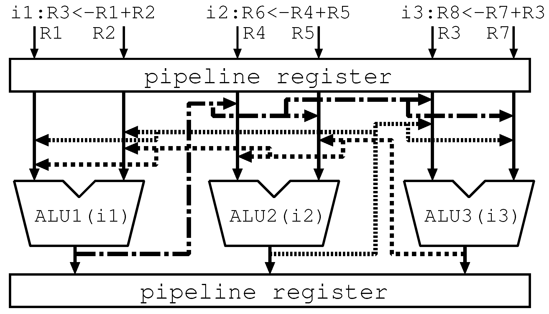
Figure 4.
Allocation and Forwarding paths of Lim Path.
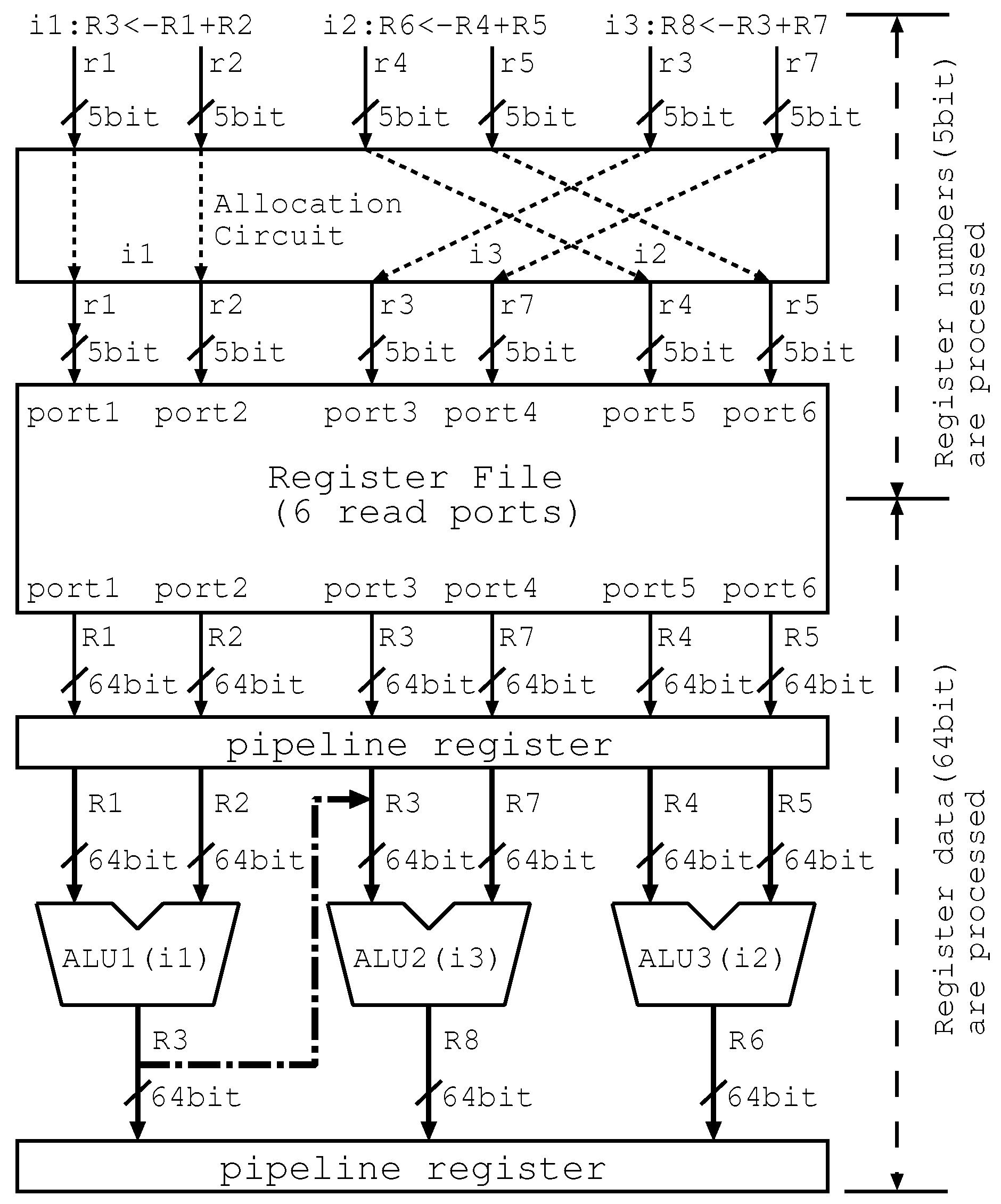
Figure 5.
Bypass Circuits of Full Path.

Figure 6.
Bypass Circuits of Lim Path(1 Output to 2 ALU).
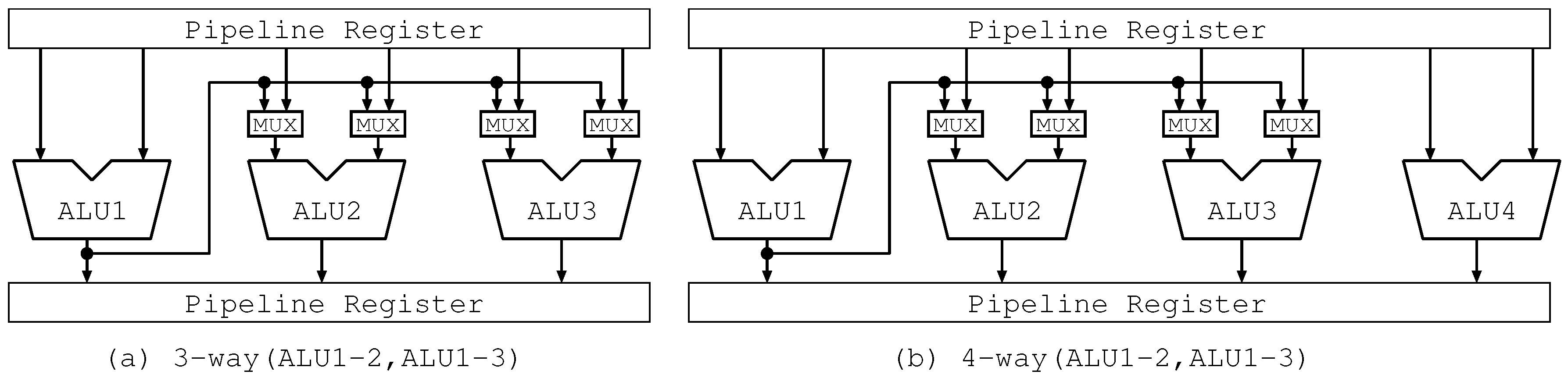
Figure 7.
Bypass Circuits of Lim Path(1 Output to 1 ALU).
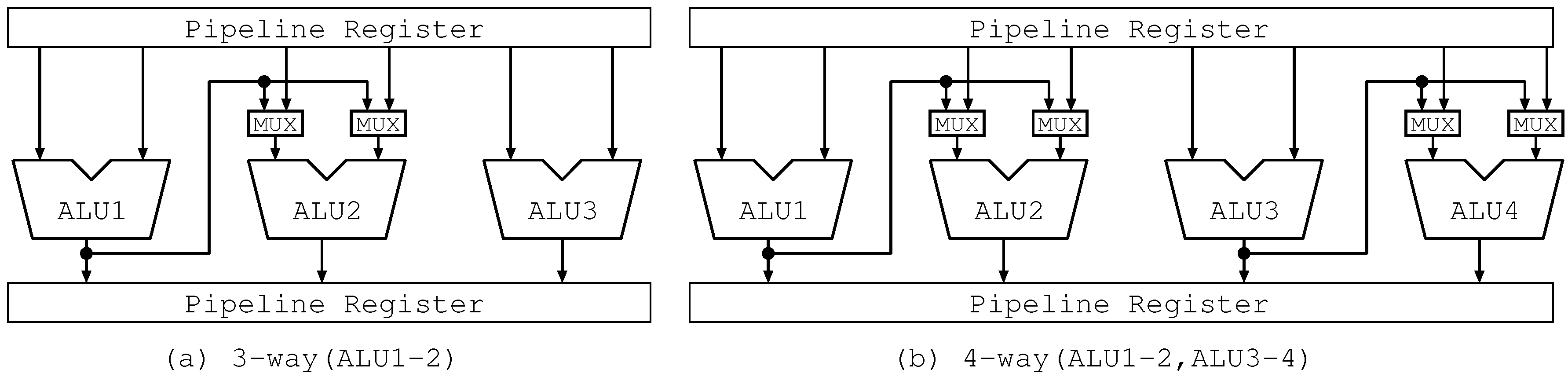
Figure 8.
Area of ALU Cascading Mechanism.

Figure 9.
Energy of ALU Cascading Mechanism.

Figure 10.
Delay of ALU Cascading Mechanism.
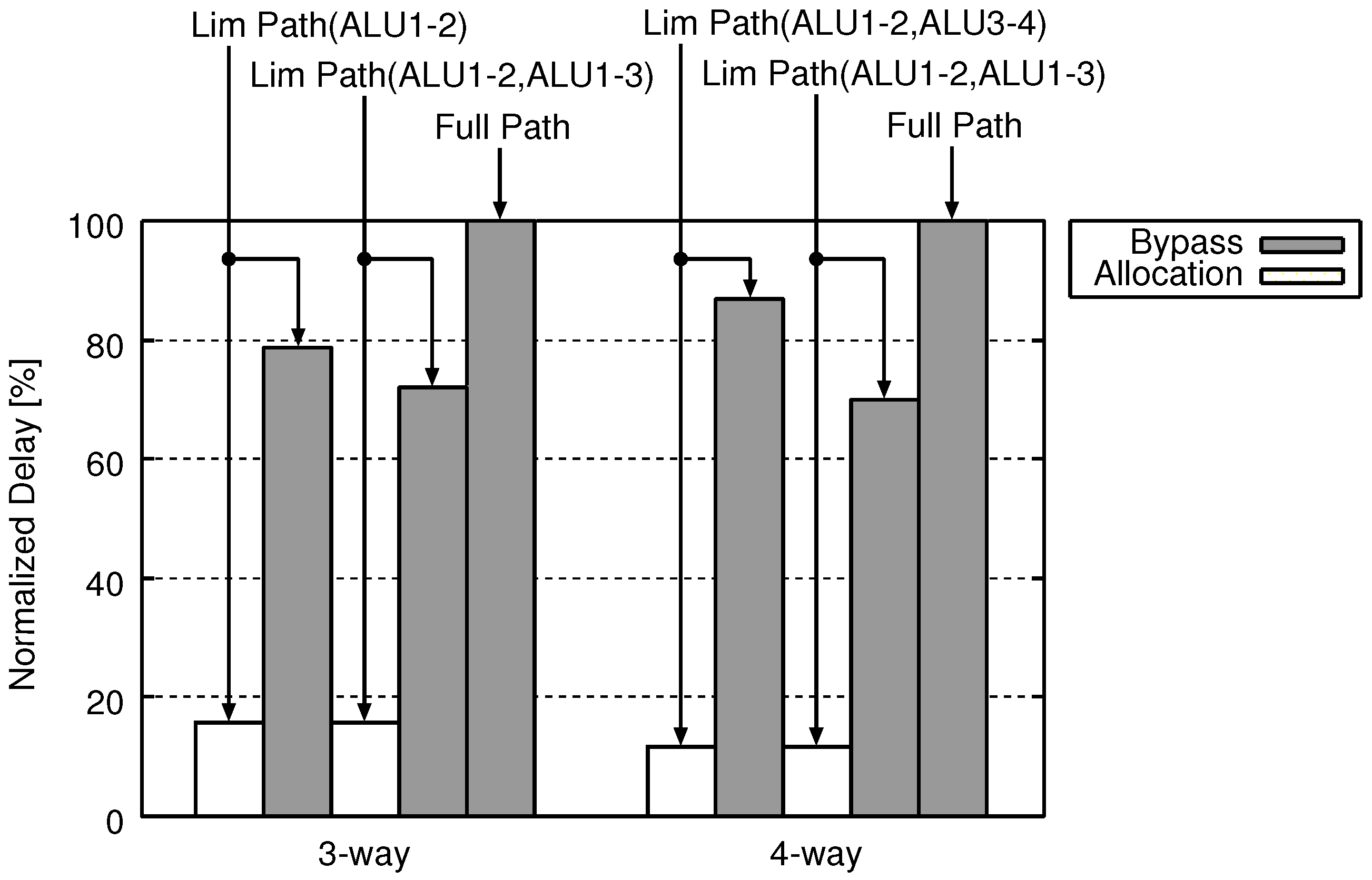
Figure 11.
IPC improvement due to ALU Cascading: (a) three-way; and (b) four-way.

Figure 12.
Cascading cancellation due to Lim Path: (a) three-way; and (b) four-way.


Table 1.
In-order Processor configurations.
| Execution Width | 3, 4-way |
| Data Width | 64-bit |
| Chain Depth | 1-chain |
| Chain Width | 1, 2 |
| Fetch Width | n instruction/cycle |
| Decode Width | n instruction/cycle |
| Issue Width | n instruction/cycle |
| Commit Width | n instruction/cycle |
| Functional Unit | n iALU, 2 iMULT/DIV, n fpALU, |
| 2 fpMULT/DIV/SQRT | |
| L1 I-cache | 32KB, 8 way, 32 byte cache line, |
| 2 cycle hit latency, | |
| L1 D-cache | 32KB, 8 way, 32 byte cache line, |
| 2 cycle hit latency | |
| L2 cache | 1MB, 16 way, 64 byte cache line, |
| 12 cycle hit latency | |
| Main memory | 8 byte/cycle band width, |
| 72 cycle first hit latency, | |
| 1 cycle burst interval | |
| L1 I-TLB | 32 entry, 4 way, 4KB page, |
| 80 cycle first hit latency | |
| L1 D-TLB | 64 entry, 4 way, 4KB page, |
| 80 cycle first hit latency | |
| Branch predictor | gshare (13 bit history, 32K entry PHT), |
| 4096 entry BTB, 32 entry RAS, | |
| 7 cycle miss penalty |
© 2017 by the authors. Licensee MDPI, Basel, Switzerland. This article is an open access article distributed under the terms and conditions of the Creative Commons Attribution (CC BY) license (http://creativecommons.org/licenses/by/4.0/).
Share and Cite
MDPI and ACS Style
Kobayashi, R.; Suzuki, A.; Shimada, H. Forwarding Path Limitation and Instruction Allocation for In-Order Processor with ALU Cascading. J. Low Power Electron. Appl. 2017, 7, 32. https://doi.org/10.3390/jlpea7040032
AMA Style
Kobayashi R, Suzuki A, Shimada H. Forwarding Path Limitation and Instruction Allocation for In-Order Processor with ALU Cascading. Journal of Low Power Electronics and Applications. 2017; 7(4):32. https://doi.org/10.3390/jlpea7040032
Chicago/Turabian StyleKobayashi, Ryotaro, Anri Suzuki, and Hajime Shimada. 2017. "Forwarding Path Limitation and Instruction Allocation for In-Order Processor with ALU Cascading" Journal of Low Power Electronics and Applications 7, no. 4: 32. https://doi.org/10.3390/jlpea7040032
Note that from the first issue of 2016, this journal uses article numbers instead of page numbers. See further details here.