A Performance of the Soft-Charging Operation in Series of Step-Up Power Switched-Capacitor Converters

Daniel Felix Ritchie School of Engineering & Computer Science, University of Denver, 2155 E Wesley Ave, Denver, CO 80208, USA
*
Author to whom correspondence should be addressed.
J. Low Power Electron. Appl. 2018, 8(1), 8; https://doi.org/10.3390/jlpea8010008
Submission received: 8 February 2018
/
Revised: 3 March 2018
/
Accepted: 11 March 2018
/
Published: 12 March 2018
Abstract
:Due to their high power density and appropriateness for small circuits integration, switched-capacitor (SC) converters have gotten more interests. Applying the soft-charging technique effectively eliminates the current transient that results in a higher power density and a higher fundamental efficiency. Achieving the complete soft-charging operation is impossible by using the conventional control diagram for any SC converter topology. In this paper, we proposed a split-phase control to achieve the complete soft-charging operation in a power switched-capacitor (PSC) converter. The proposed control diagram was designed for a 1-to-4 PSC converter (two-level of the PSC converter). The implemented split-phase diagram successfully controls eight switches to exhibit eight modes of operation. In addition to the current transient elimination, the complete soft-charging allows us to reduce capacitor sizes. However, reducing capacitor size negatively increases the output voltage ripple; hence, an output LC filter is needed. The complete soft-charging achievement accomplishes a 96% efficiency due to the lower output impedance and the dead time switching. LT-Spice software has been used to verify the proposed control and the results were compared with hard-charging and incomplete soft-charging operations.
1. Introduction
DC-to-DC converters are commonly designed with magnetic elements for energy storing purposes. Designing a DC-to-DC converter with magnetic components such as an inductor leads to low power density due to the inductor bulky size. An increase in the power density of DC-to-DC converters requires a higher switching frequency () since the inductor size is inversely proportionate to the switching frequency. Increasing the can solve the problem partially; however, it will cause a switching loss produced by semiconductor elements. A growth in switching loss is conversely proportional to the converter efficiency [1,2]. High power density and high efficiency are two significant requirements for designing a DC-to-DC converter functional for tiny electronic circuit integration.
To satisfy these desires, the DC-to-DC switched-capacitors (SC) converters are widespread for on-chip integration. Because the DC-to-DC SC converters contain only capacitors and switches, they have a high-power density. Charging and discharging the capacitors allow the electric charge to flow from the input to the output to accomplish voltage regulation by alternating the switches states. In addition to the high-power density, the SC converters tend to maintain the efficiency at a high voltage gain. Because of their numerous topologies, analysis of the SC converters has been considered a challenging task. The SC analysis has been generalized in [3]. Two operation states occur in most types of SC converter, which are charging and discharging modes. The total charge of the charging mode is assumed to equal the total charge in the discharging mode [3]. By studying the charge flow, the SC converter voltage gain, the slow switching limit (SSL), and the fast switching limit (FSL) can be obtained. The output impedance at the SSL limit is proportional to the switching frequency, and the capacitors’ sizes while the output impedance at the FSL limit depends on the switches resistance [4].
However, the SC converters are not ideal or without drawbacks. For instance, providing a higher voltage gain is unlikely to be achieved with SC converters. Furthermore, the SC converters cannot normalize the output voltage in a lossless approach due to the resistors [5,6,7,8]. The proposed step-up PSC converter has demonstrated a higher gain voltage at a smaller number of elements compared to other SC topologies. The PSC converter has a gain voltage where is the number of stages. Each added stage requires two additional capacitors and four more switches [7]. Unlike the other SC converters’ topologies, the number of operation modes increase with the number of levels. Each level of the PSC converter has two operation modes. For instance, the 1-to-4 PSC converter (two-levels) as in Figure 1 operates in four operation modes, where three-levels operate in six operation modes. To achieve a superior efficiency achievement purpose, it is recommended that SC converters are designed with resonant soft-switching techniques. However, designing resonant SC converters requires additional components, and hence a reduction in the power density is possible [9,10,11,12,13,14,15,16,17].
The work in [18,19,20,21,22,23,24] proposed an alternative way of soft switching which is called a soft-charging operation. The main advantage of applying the soft-charging technique instead of soft-switching is it is not essential to add more components to optimize the fundamental efficiency [18]. Eliminating the current transient to increase the fundamental efficiency and the power density are the major functions of the soft-charging technique. In conventional operation (hard-charging), there are two ways to reduce the current transient, either by large capacitors selection or a higher . However, these two implementations reduce the power density and the fundamental efficiency respectively. To overcome the current transient issue, the complete soft-charging techniques are proposed to achieve that with a lower and smaller capacitors [22]. Resizing the capacitors in soft-charging techniques can be done theoretically by analyzing the voltage change and charge flow for each capacitor. In addition to resizing the capacitors, the output capacitor is eliminated in the soft-charging technique. Incomplete soft-charging and complete soft-charging are the two types of soft-charging. One significant difference between them is the complete soft-charging operation operates in a split-phase control diagram. The proposed control for Dickson SC converter [23] splits each operation mode into two modes, which are the conventional modes besides the transition modes.
In this paper, the complete soft-charging operation has been applied to the proposed PSC converter in [7]. A control diagram has been proposed to achieve a complete soft-charging in a 1-to-4 PSC converter. Achieving the complete soft-charging shows an output impedance reduction and a superior efficiency achievement to the 1-to-4 PSC converter. In addition, the split-phase successfully recovered the current transient. The reason for that is due to the dead time of the control diagram. However, reducing the capacitor size caused a high output voltage ripple. To overcome the ripple issues, an output LC filter has been inserted into the 1-to-4 PSC converter. The rest of the paper will be organized as follows: Section 2 will contain series of PSC converters, topology, and operation, and then the incomplete soft-charging operation of the second order PSC converter comes in Section 3. In Section 4, the complete soft-charging operation of the second order PSC converter is described. The result and discussion come in Section 5 before the conclusion.
2. A Series of PSC Converters
2.1. A Second-Order PSC Converter; Topology and Operation
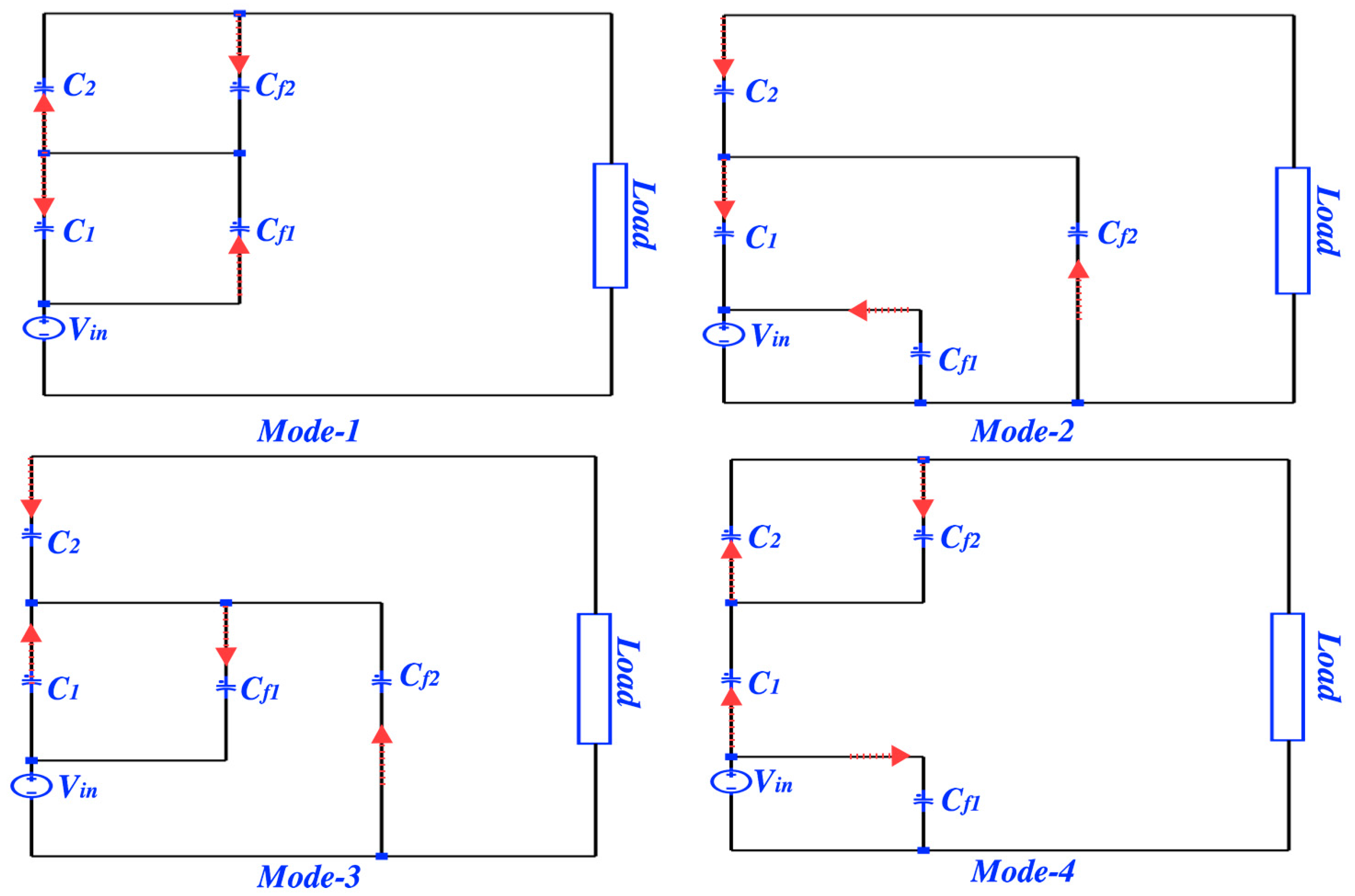
Figure 1 shows the topology of the 1-to-4 PSC converter and its control signals [7]. The control diagram in Figure 2a shows how four modes of operation are possible. The operation modes come in the following sequence: Mode-1, Mode-2, Mode-3, Mode-4, and Mode-1. In each mode, the capacitors are connected differently for voltage regulation purposes. In Mode-1 the flying capacitor is charging; however, flying capacitor is discharging. In Mode-2, both flying capacitors and are discharging, whereas they are both charging in Mode-4. In Mode-3 is discharging whereas is charging. To find the voltage gain of the proposed converter, each mode has a total charge that can be derived from the following equations.
where is the number of modes 1, 2, 3 and 4. From Mode-1 Figure 2
by substituting (2), (3) and (4) in (1) we get the total charge of Mode-1 (5)
To find the total charge of the rest of the modes, the same steps can be repeated
In the steady state operation, the total charge of any two modes is assumed to be equal. In this work, we assumed that
By simplifying (9) and (10) we get
By combining (11) and (12), the 1-to-4 PSC converter’s voltage gain can be calculated (13)
The general form of the proposed converter is
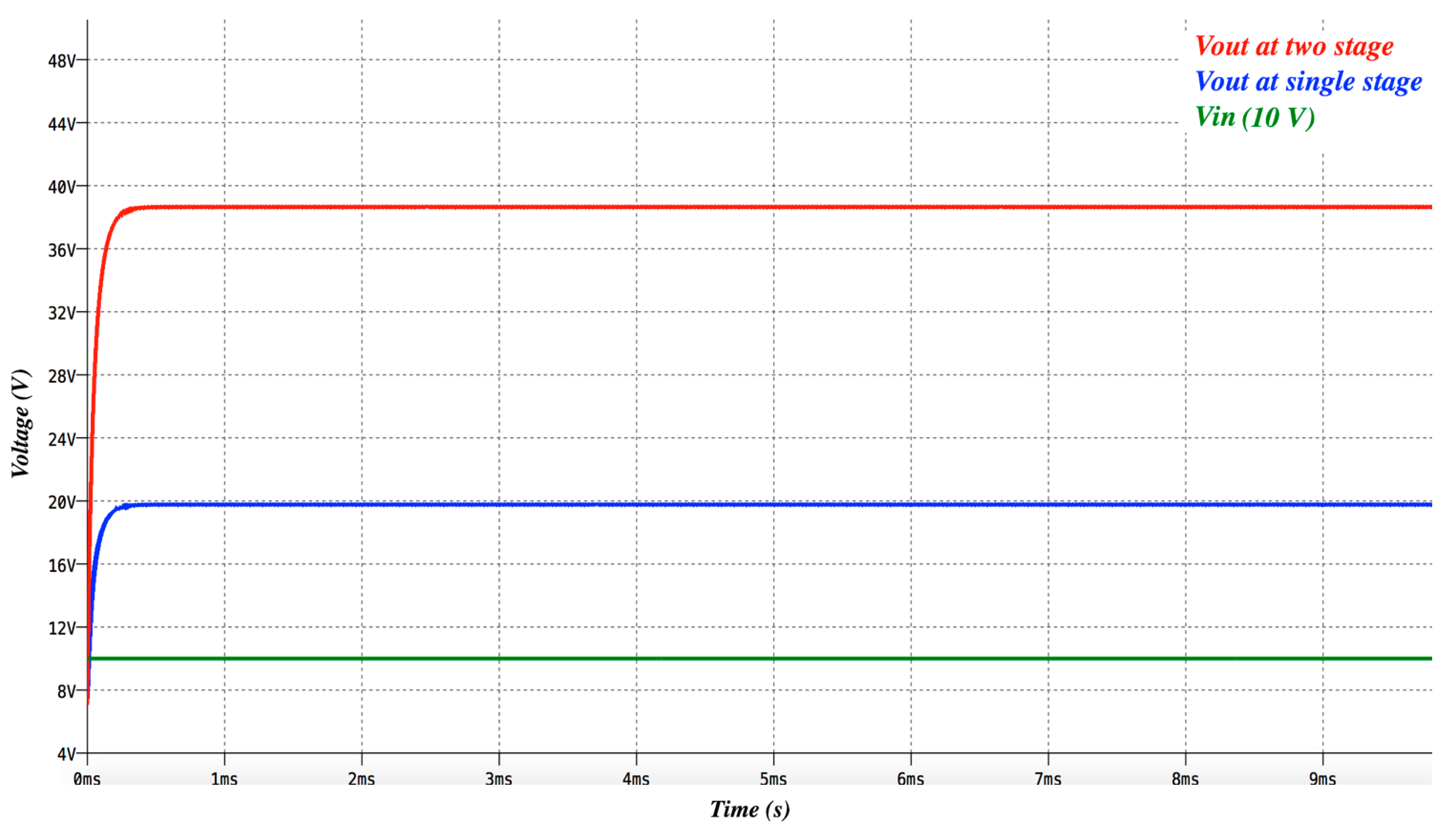
where is the number of the stage. The output voltages of the one and two stages of PSC converter are presented in Figure 3.
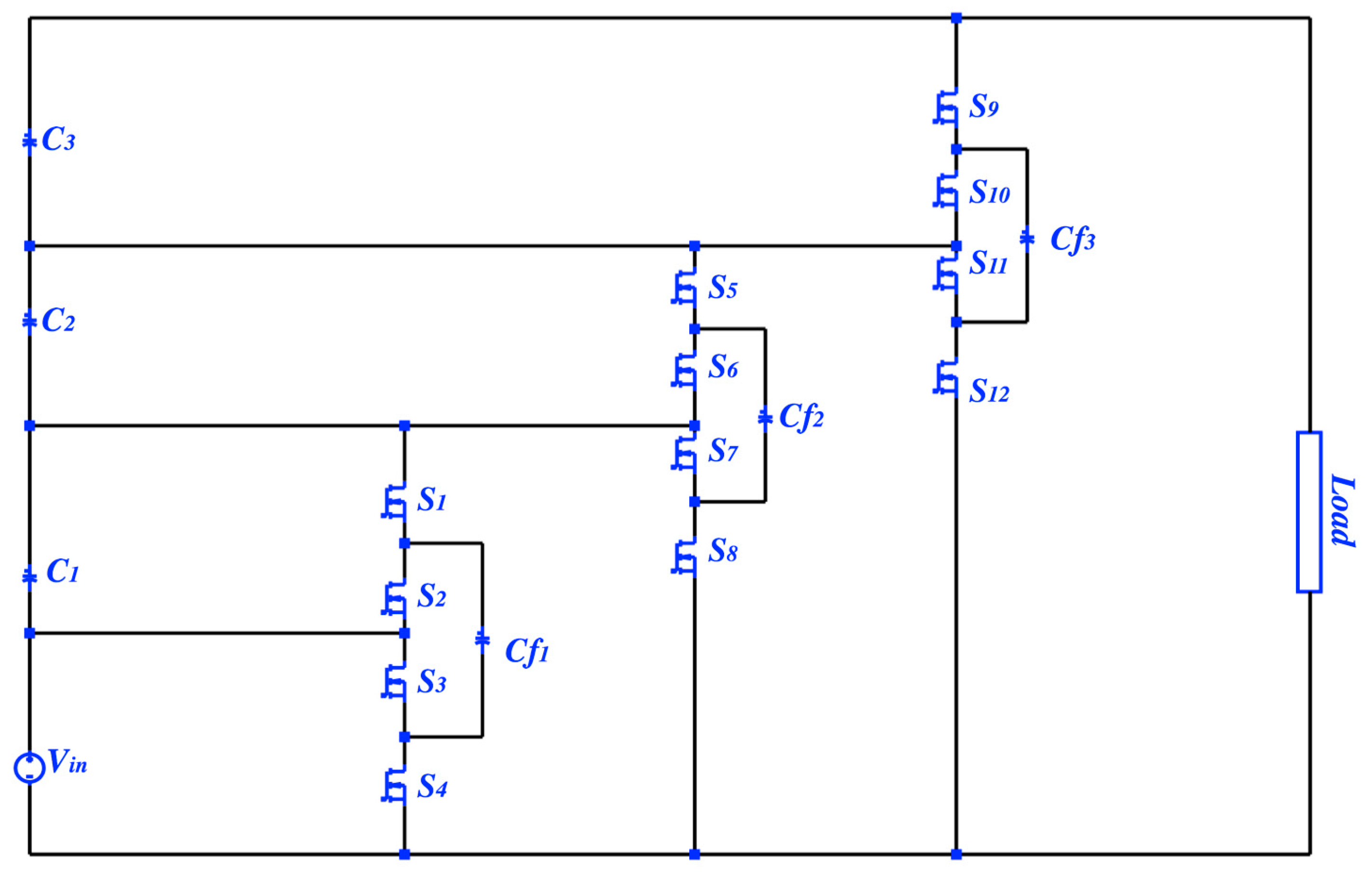
For each added stage, two capacitors and four switches are needed. Figure 4 presents three stages of the proposed converter with 1-to-8 conversion ratio.
2.2. Slow-Switching Limit Impedance ()
The SC converters suffer from losses related to the switches and the capacitors’ charging or discharging process. This capacitors’ loss can be characterized as an output impedance that is called a slow switching limit impedance, . The charge flow analysis of the four modes has been applied to find the charge multiplier of the four capacitors
In [18,19,20,21,22] a useful technique was used to find the charge flow vectors of all the operation modes. For the ith mode, KCL can be derived by (17)
where is reduced incidence matrices of the four modes of 1-to-4 PSC converter. Each row in corresponds to an independent KCL equation. The number of independent KCL equations can be derived by the number of nodes. Each element in the circuit has two nodes related to its positive and negative terminals as in Figure 5 [24,25].
To find the charge flow’s vectors, (17) can be solved for .
The total output charge with respect to the output charge can be found in (18)
The total output charge with respect to the input charge is
By using (21), (19) can be rewritten with respect to the output charge (22)
By applying (15), the charge multipliers are presented in (23)
Then by using Tellegen’s theorem, can be found for our proposed design (24).
where
2.3. Fast-Switching Limit Impedance
Another important parameter can be determined by analyzing the SC converter to find the fast switching limit (). In the SC converter, two parameters are responsible for increasing the efficiency, which are a high switching frequency and a large capacitor size. The depends on the switches’ as in the following equation
where is the charge multiplier of eight switches in the 1-to-4 PSC converter.
3. An Incomplete Soft-Charging Operation of the Second Order PSC Converter
For more convenience, a constant output current source is used as an output load in the soft-charging analysis [18,19,20,21]. In addition, the PSC converter is designed with a lossless output capacitor to recover the voltage differences. The current transient and the voltage mismatch dispersions are the essential benefits of the soft-charging technique. However in the hard-charging operation, requirements of a higher switching frequency or a larger capacitor selection are needed to eliminate the current transient. To determine the flowing charge and the changing capacitors’ voltage for the 1-to-4 PSC converter, we applied a KCL. Corresponding to the timing diagram in Figure 2a, four operation modes are presented in Figure 2b. The elements of each circuit in Figure 2b, which are , can be written in a voltage vector form.
Each phase in Figure 2b has four possible loops that can be expressed in a reduced matrix loop (29) [24]
the reduced matrix’s loops for the four modes can be written as in (29),
At the end of each mode, the voltage vectors become
where is the voltage change related to the load received charge. From (28) and (30), we have
In the steady state assumption, the total voltages changes for the four operation modes equal zero.
since is a constant DC source, then . To satisfy a row with is added to
where are null spaces of the modified matrices (after adding ).
The voltage change can be calculated by
where , , , , and can be found by (36), and are the reduced form of and (after eliminating the last row corresponding to ). The is zero at an inductive load case.
Now (35) can be solved to calculate .
From (19) and (38) the capacitor sizes can be found by (39)
4. A Complete Soft-Charging Operation of the Second Order PSC Converter
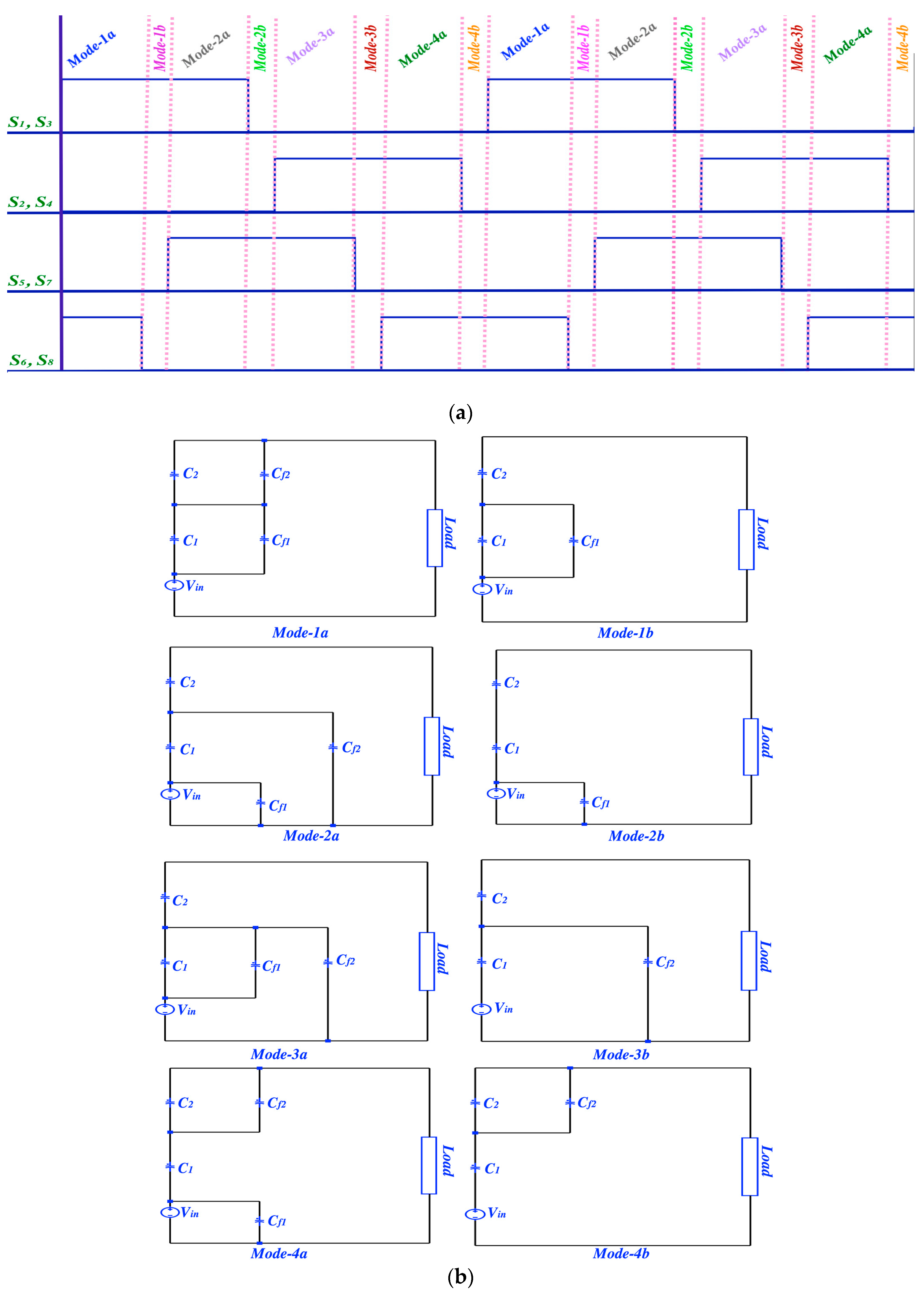
The complete soft-charging analysis can be satisfied if and only if the KVL exists at all operation modes including the four transitions modes. In this section, we proposed a split-phase control for the 1-to-4 PSC converter. The control diagram in Figure 6a allows eight modes of operation to exist as in Figure 6b. Four of those modes are the same as the four modes of the conventional PSC converter Figure 2b where the new four modes are basically the transition modes. The same procedures as applied for the incomplete soft-charging are repeated in this section. The and matrices Mode-1a, Mode-2a, Mode-3a and Mode-4a are the same matrices as in Section 2. Since the extra four transition modes have three capacitors then only two KVL loops are possible for matrices, which are presented as in following reduced loop.
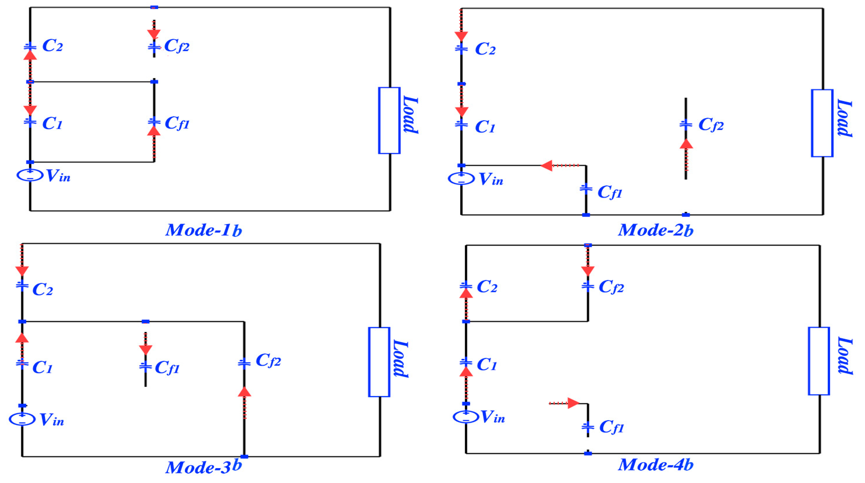
Although the transition modes contain three capacitors, their charge flow directions are the same as the charge flow direction of the basic modes as in Figure 5. However, the number of nodes in the transition modes is five instead of four due to the floating capacitor terminals. Since both terminals are floating, they are considered one node and expressed in an extra row in . By using (17), the reduced matrices of the transition modes as in Figure 7 are presented as following (41).
By applying the (17) the charge flow of the eight modes are
from (42), the last rows represent the output delivered charge. The total input charge equals 16 which is the sum of the input charges for all eight modes (42). The duty cycle of each mode to achieve a complete soft-charging is calculated in (43). Each mode has a certain duty cycle where the sum of the modes’ duty cycles completes one period of the proposed split-phase control in Figure 6a.
The complete soft-charging operation allows us to resize the capacitors; however, small capacitor selection can result in a higher voltage ripple. To overcome the voltage’s ripple, an output LC filter can be added to the output stage of the PSC converter. Figure 8 shows a 1-to-4 PSC with an output LC filter.
5. Results and Discussion
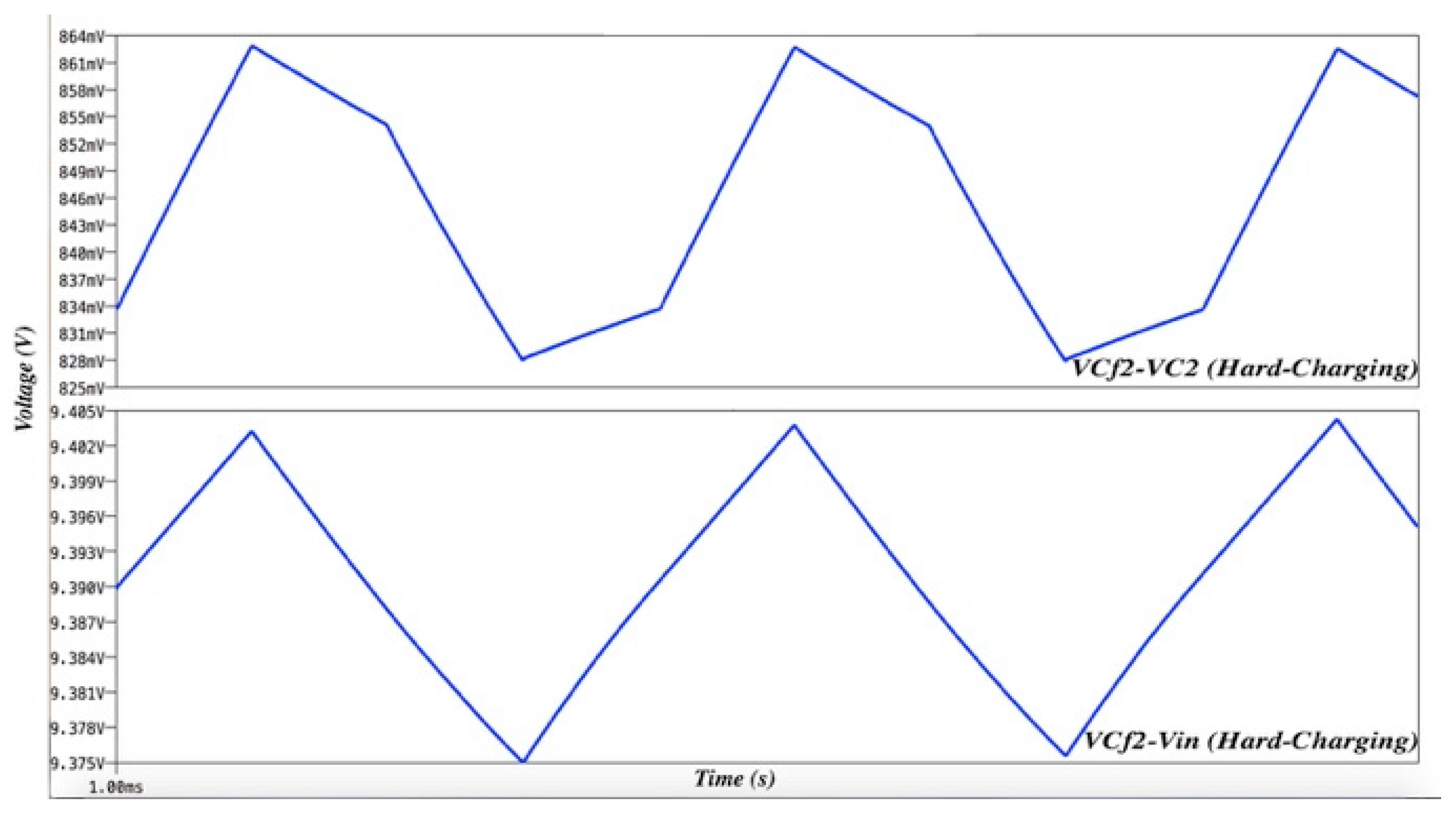
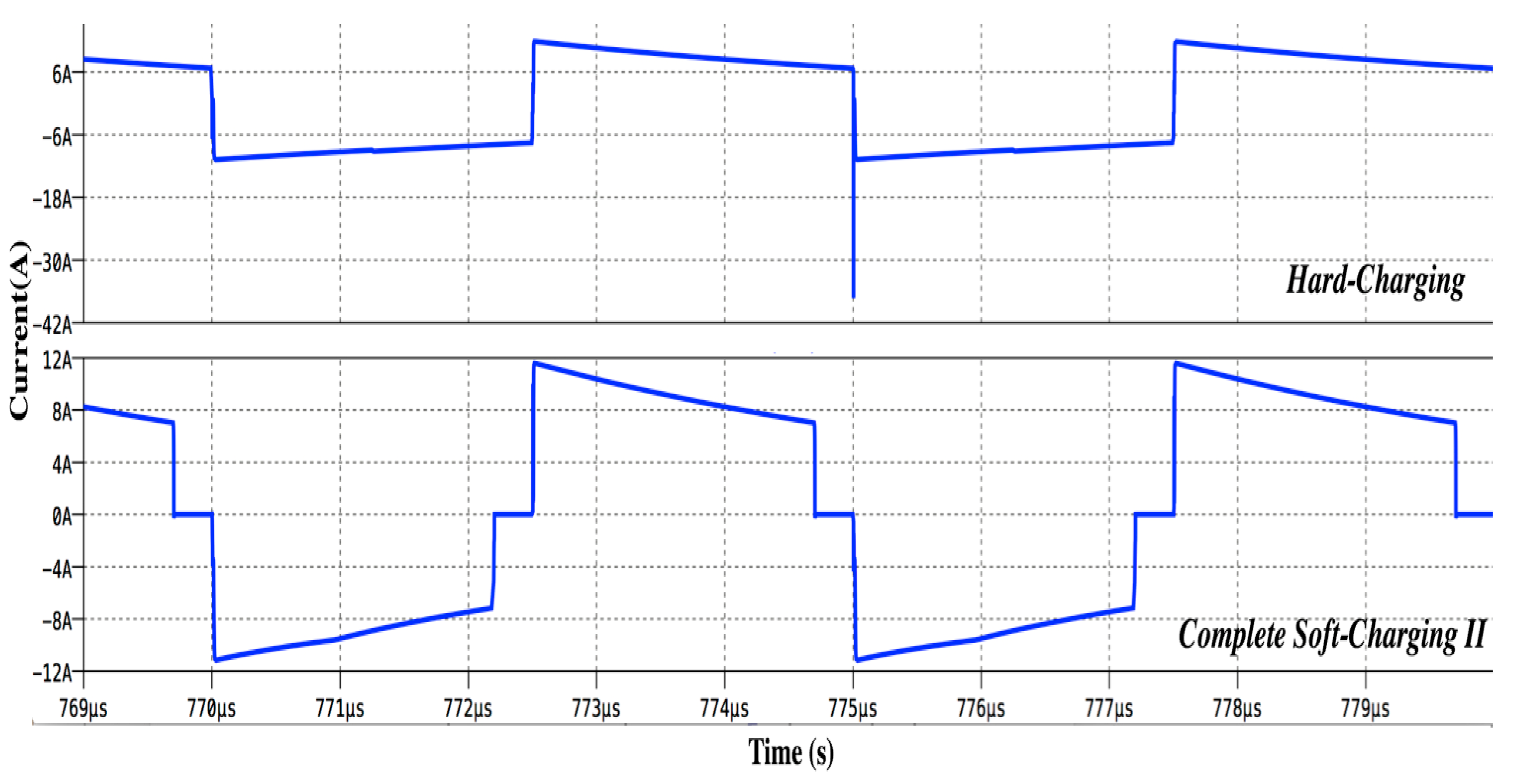
The simulation design has been completed to determine the proposed split-phase control for the 1-to-4 PSC converter. The proposed split-phase control successfully supports the 1-to-4 PSC converter to achieve its complete soft-charging operation. Eight operation modes are approached in the following sequences, Mode 1-a, Mode 1-b, Mode 2-a, Mode 2-b, Mode 3-a, Mode 3-b, Mode 4-a and Mode 4-b in the soft-charging operation. However, only four operation modes were possible by controlling them conventionally, Figure 2. The scheme needs eight switches and four capacitors to rate a 40 V nominal output voltage with a supplied voltage of 10 V. The voltage stresses across the switches either 0.25 or 0.5 as. Due to the switches’ stresses and the rated output voltage, all eight switches are selected to rate 40 V. Direct comparisons among four operation techniques, which are hard-charging, incomplete soft-charging, complete soft-charging-I and complete soft-charging-II, are presented in this section. In the hard-charging approach, , , and are selected equally with a capacitance equal to 188 µF. Corresponding to (38), and have the lowest voltage change; and have the highest voltage change. Hence by using (39) and are selected differently (Section 3 and Section 4). In the incomplete soft-charging and complete soft-charging-I operations, and have a size equals to half of the and as in Table 1 which are 90 µF and 188 µF respectively. Due to the switching dead time, the proposed split-phase control allows for more decrease of and sizes. The converter with reduced capacitors is referred to as a complete soft-charging-II in Table 2. Reducing the capacitors sizes outcomes in a lower output impedance. Figure 9 shows the output impedance versus the switching frequency at hard-charging, incomplete soft-charging and complete soft-charging-II. It can be clearly seen that the output impedance eventually decreases at a higher switching frequency selection. However, unlike the hard-charging operation, applying the complete soft-charging-II technique keeps the output impedance almost constant at varied switching frequencies. Having an almost constant output impedance means the 1-to-4 PSC converter participates the FSL limits at a lower . Moreover, the split-phase control helps to eliminate the voltage mismatch between any two parallel capacitors. The voltage mismatch between and has been recovered by applying split-phase control as in Figure 10 and Figure 11. In addition to eliminating the voltage mismatch, the complete soft-charging removes the current transient in the flying capacitors as in Figure 12. The decrease of the output impedance and the dead time switching should effectively recover the fundamental efficiency. However, reducing capacitor size causes an undesired higher output voltage ripple. To overcome the output voltage ripple, an output filter was added to the PSC converter as presented in Figure 9. (44), shows an equation to determine where is the equivalent capacitance in the 1-to-4 PSC converter [22].
The general output impedance in the SC converters can be calculated by using (45) [22]
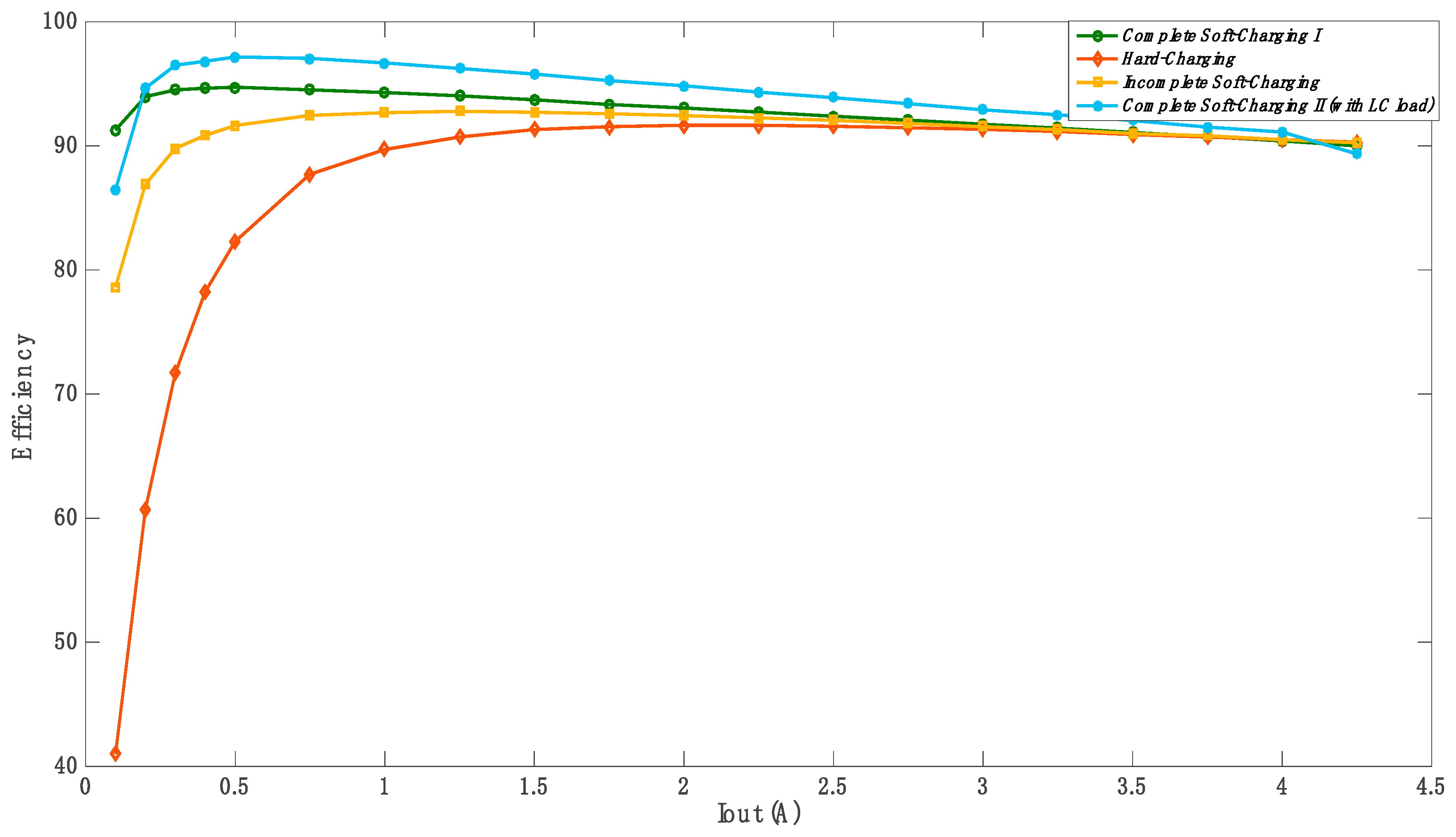
Figure 13 shows the 1-to-4 PSC efficiency against the in four compared operations. The highest achieved efficiency occurs at the complete soft-charging-II with the filter insertion. Adding the filter could decrease the efficiency; however, this reduction is small compared to the high increase of the efficiency by using the soft-charging-II operation.
6. Conclusions
The proposed split-phase control allows the 1-to-4 PSC converter to operate in the complete soft-charging operation. The elimination of the current transient excellently increases both the efficiency and the power density. In addition to the output impedance reduction, the complete soft-charging operation leads to eliminating the voltage mismatch between any parallel capacitors. A theoretical analysis was successfully applied for resizing the capacitors in the soft-charging approach. Beyond the resizing approach, the theoretical analysis productively helps to calculate the duty cycles for each operation mode. The dead time of the proposed control diagram is the main reason behind achieving superior efficiency due to smaller switching losses and lower output impedance. However, a lower capacitor size causes a higher output voltage ripple. An output LC filter was added to the 1-to-4 PSC converter to reduce the output voltage ripple. Although adding the LC filter could cause a small loss; however, this loss is not effective to the efficiency which has been efficaciously increased by using the complete soft-charging-II technique.
Acknowledgments
We would like to thank Daniel Felix Ritchie School of Engineering & Computer Science, University of Denver, for supporting us to successfully complete this work.
Author Contributions
Ayoob Alateeq conceived and designed the experiments; Ayoob Alateeq performed the experiment simulations; Ayoob Alateeq, Yasser Almalaq and Mohammad Matin analyzed the result; Ayoob Alateeq wrote the paper.
Conflicts of Interest
The authors declare no conflict of interest.
References
- Almalaq, Y.; Alateeq, A.; Matin, M. Non-isolated high gain switched inductor DC-DC multilevel cuk converter for photovoltaic applications. In Proceedings of the 2017 North American Power Symposium (NAPS), Morgantown, WV, USA, 17–19 September 2017. [Google Scholar]
- Seeman, M.D.; Sanders, S.R. Analysis and Optimization of Switched-Capacitor DC–DC Converters. IEEE Trans. Power Electron. 2008, 23, 841–851. [Google Scholar] [CrossRef]
- Alateeq, A.; Almalaq, Y.; Matin, M. Using SiC MOSFET in switched-capacitor converter for high voltage applications. In Proceedings of the 2016 North American Power Symposium (NAPS), Denver, CO, USA, 18–20 September 2016; pp. 1–5. [Google Scholar]
- Xiong, S.; Wong, S.C.; Tan, S.C. A series of exponential step-down switched-capacitor converters and their applications in two-stage converters. In Proceedings of the 2013 IEEE International Symposium on Circuits and Systems (ISCAS2013), Beijing, China, 19–23 May 2013; pp. 701–704. [Google Scholar]
- Xiong, S.; Wong, S.C.; Tan, S.C.; Tse, C.K. Optimal Design of Complex Switched-Capacitor Converters via Energy-Flow-Path Analysis. IEEE Trans. Power Electron. 2017, 32, 1170–1185. [Google Scholar] [CrossRef]
- Xiong, S.; Wong, S.C.; Tan, S.C.; Tse, C.K. A Family of Exponential Step-Down Switched-Capacitor Converters and Their Applications in Two-Stage Converters. IEEE Trans. Power Electron. 2014, 29, 1870–1880. [Google Scholar] [CrossRef] [Green Version]
- Alateeq, A.S.; Almalaq, Y.A.; Matin, M.A. Modeling and simulation of GaN step-up power switched capacitor converter. In Proceedings of the Wide Bandgap Power Devices and Applications II, San Diego, CA, USA, 7–8 August 2017. [Google Scholar]
- Kesarwani, K.; Sangwan, R.; Stauth, J.T. Resonant-Switched Capacitor Converters for Chip-Scale Power Delivery: Design and Implementation. IEEE Trans. Power Electron. 2015, 30, 6966–6977. [Google Scholar] [CrossRef]
- Cheng, K. New generation of switched capacitor converters. In Proceedings of the 29th IEEE Annual Power Power Electronics Specialists Conference, Fukuoka, Japan, 22 May 1998; Volume 2, pp. 1529–1535. [Google Scholar]
- Zhang, Y.; Gao, Y.; Zhou, L.; Sumner, M. A Switched-Capacitor Bidirectional DC-DC Converter with Wide Voltage Gain Range for Electric Vehicles with Hybrid Energy Sources. IEEE Trans. Power Electron. 2018. [Google Scholar] [CrossRef]
- Keiser, O.; Steimer, P.K.; Kolar, J.W. High power resonant Switched-Capacitor step-down converter. In Proceedings of the 2008 IEEE Power Electronics Specialists Conference, Rhodes, Greece, 15–19 June 2008; pp. 2772–2777. [Google Scholar]
- Shang, Y.; Cui, N.; Zhang, Q.; Zhang, C. A battery equalizer with zero-current switching and zero-voltage gap among cells based on three-resonant-state LC converters. In Proceedings of the 2017 IEEE Applied Power Electronics Conference and Exposition (APEC), Tampa, FL, USA, 26–30 March 2017; pp. 1647–1651. [Google Scholar]
- Beiranvand, R. Regulating the Output Voltage of the Resonant Switched-Capacitor Converters below Their Resonant Frequencies. IEEE Trans. Ind. Electron. 2017, 64, 5236–5249. [Google Scholar] [CrossRef]
- Shen, M. A zero voltage switching switched capacitor voltage doubler. In Proceedings of the 2012 IEEE International Symposium on Industrial Electronics, Hangzhou, China, 28–31 May 2012; pp. 131–136. [Google Scholar]
- Lim, S.; Otten, D.M.; Perreault, D.J. Power conversion architecture for grid interface at high switching frequency. In Proceedings of the IEEE Applied Power Electronics Conference and Exposition, Fort Worth, TX, USA, 16–20 March 2014; pp. 1838–1845. [Google Scholar]
- Arntzen, B.; Maksimovic, D. Switched-capacitor DC/DC converters with resonant gate drive. IEEE Trans. Power Electron. 1998, 13, 892–902. [Google Scholar] [CrossRef]
- Yang, J.W.; Do, H.L. Soft-Switching Bidirectional DC-DC Converter Using a Lossless Active Snubber. IEEE Trans. Circuits Syst. I Regul. Pap. 2014, 61, 1588–1596. [Google Scholar] [CrossRef]
- Lei, Y.; Pilawa-Podgurski, R.C.N. Analysis of Switched-capacitor DC-DC Converters in Soft-charging Operation. In Proceedings of the 2013 IEEE 14th Workshop on Control and Modeling for Power Electronics (COMPEL), Salt Lake City, UT, USA, 23–26 June 2013; pp. 1–7. [Google Scholar]
- Lei, Y.; May, R.; Pilawa-Podgurski, R.C.N. Split-phase control: Achieving complete soft-charging operation of a dickson switched-capacitor converter. In Proceedings of the 2014 IEEE 15th Workshop on Control and Modeling for Power Electronics (COMPEL), Cantabria, Spain, 22–25 June 2014; pp. 1–7. [Google Scholar]
- Lei, Y.; Pilawa-Podgurski, R.C.N. A General Method for Analyzing Resonant and Soft-Charging Operation of Switched-Capacitor Converters. IEEE Trans. Power Electron. 2015, 30, 5650–5664. [Google Scholar] [CrossRef]
- May, R. Analysis of Soft Charging Switched Capacitor Power Converters. Master’s Thesis, University of Illinois, Urbana Champaign, IL, USA, August 2013. [Google Scholar]
- Lei, Y.; May, R.; Pilawa-Podgurski, R. Split-Phase Control: Achieving Complete Soft-Charging Operation of a Dickson Switched-Capacitor Converter. IEEE Trans. Power Electron. 2016, 31, 770–782. [Google Scholar] [CrossRef]
- Lei, Y. High Performance Power Converters Leveraging Capacitor-Based Energy Transfer. Ph.D. Thesis, University of Illinois, Urbana Champaign, IL, USA, 2017. [Google Scholar]
- Chua, L.O.; Desoer, C.A.; Kuh, E.S. Linear and Nonlinear Circuits; McGraw-Hill Book Company: New York, NY, USA, 1987. [Google Scholar]
- Henry, J.M.; Kimball, J.W. Switched-Capacitor Converter State Model Generator. IEEE Trans. Power Electron. 2012, 27, 2415–2425. [Google Scholar] [CrossRef]
Figure 1.
A 1-to-4 PSC topology (two-stage).
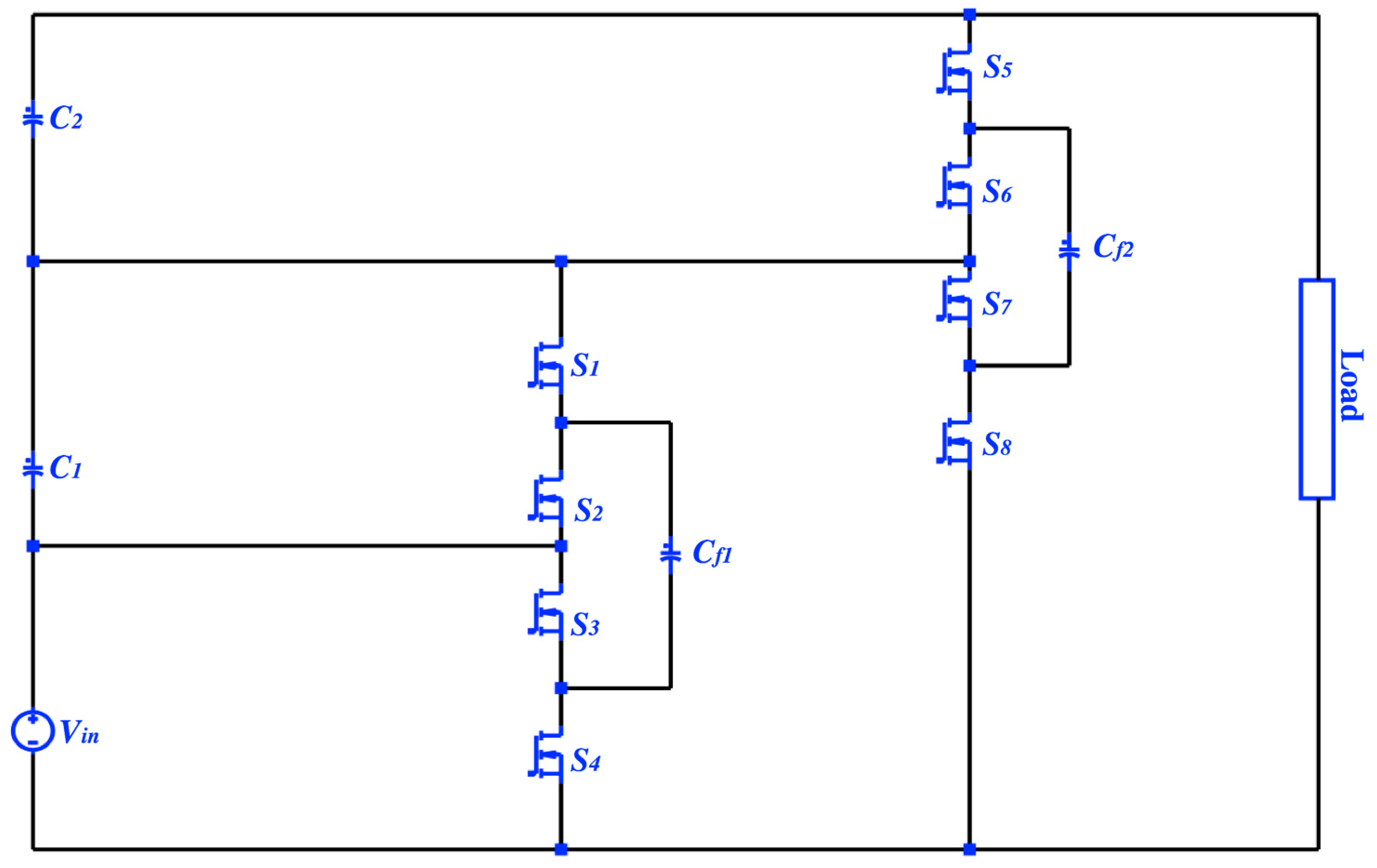
Figure 2.
(a) Timing diagram of a 1-to-4 PSC topology; (b) four-mode operation of a 1-to-4 PSC converter.
Figure 2.
(a) Timing diagram of a 1-to-4 PSC topology; (b) four-mode operation of a 1-to-4 PSC converter.
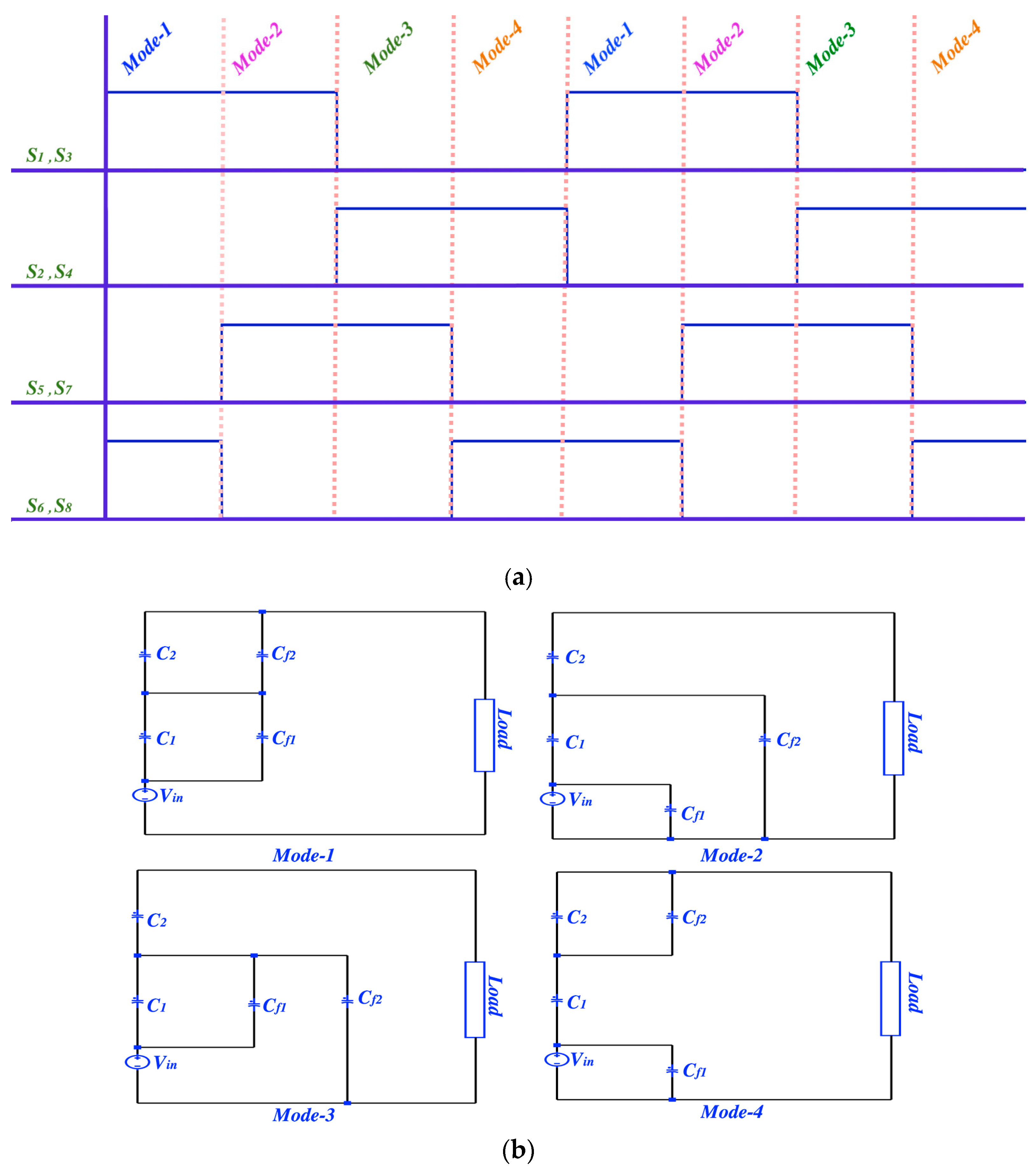
Figure 3.
The input and output voltages of a 1-to-4 and 1-to-2 of the proposed PSC converter.

Figure 4.
A 1-to-8 PSC topology (three-stage).

Figure 5.
The charge flow for the operation modes in the 1-to-4 PSC converter.

Figure 6.
(a) A proposed timing diagram to achieve a complete soft-charging in the 1-to-4 PSC converter; (b) eight operation modes of the 1-to-4 PSC converter in the complete soft-charging technique.
Figure 6.
(a) A proposed timing diagram to achieve a complete soft-charging in the 1-to-4 PSC converter; (b) eight operation modes of the 1-to-4 PSC converter in the complete soft-charging technique.

Figure 7.
The charge flow for the operation modes in the 1-to-4 PSC converter.

Figure 8.
The 1-to-4 PSC topology with an output LC filter.
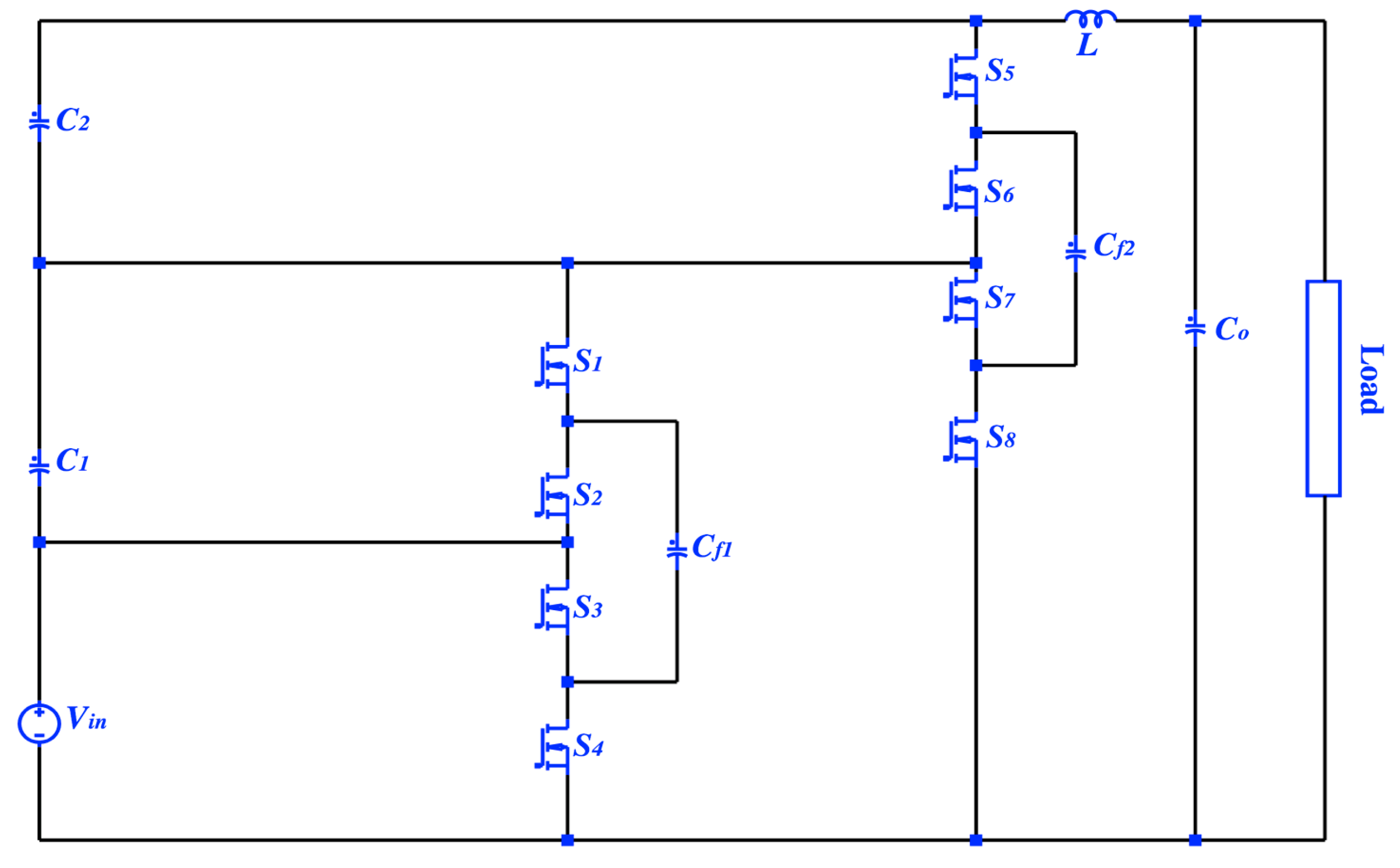
Figure 9.
Simulation output impedance of the 1-to-4 PSC converter vs. the switching frequency at three charging methods: hard-charging, incomplete soft-charging, complete soft-charging II.
Figure 9.
Simulation output impedance of the 1-to-4 PSC converter vs. the switching frequency at three charging methods: hard-charging, incomplete soft-charging, complete soft-charging II.
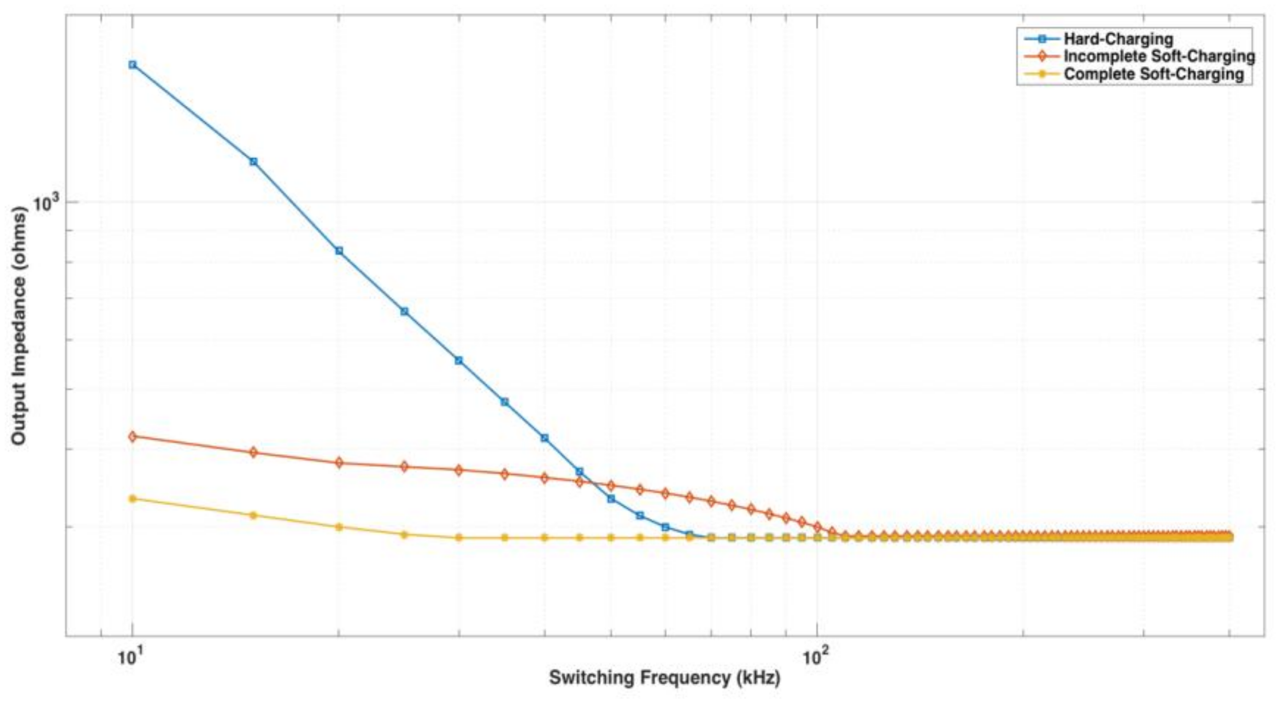
Figure 10.
Capacitor voltage mismatch during hard-charging between and .

Figure 11.
The elimination of the capacitor voltage mismatch during complete soft-charging II between and .
Figure 11.
The elimination of the capacitor voltage mismatch during complete soft-charging II between and .
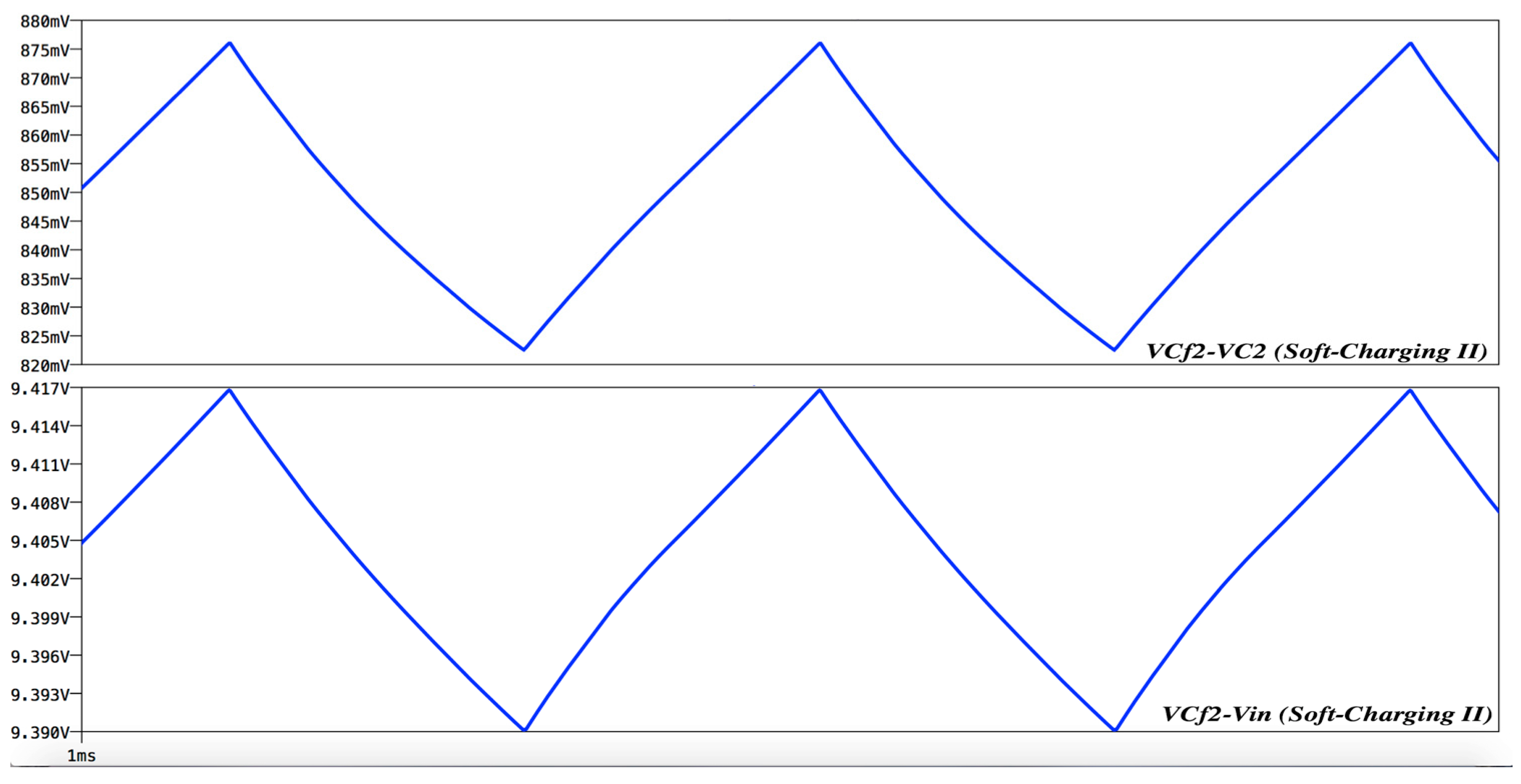
Figure 12.
The current waveform of shows the transient in the hard-charging was eliminated by applying the complete soft-charging II.
Figure 12.
The current waveform of shows the transient in the hard-charging was eliminated by applying the complete soft-charging II.

Figure 13.
The PSC converter efficiency vs. the rated power at different operation techniques: hard-charging, incomplete soft-charging, complete soft-charging I and complete soft-charging II (with LC filter).
Figure 13.
The PSC converter efficiency vs. the rated power at different operation techniques: hard-charging, incomplete soft-charging, complete soft-charging I and complete soft-charging II (with LC filter).

Table 1.
Equation of the voltage stress on all semiconductor and capacitors.
| Elements | Equation |
|---|---|
Table 2.
Simulation parameters.
| Parameter | Value |
|---|---|
| 10 V | |
| 200 KHz | |
| 188 µF | |
| 94 µF | |
| 188 µF | |
| 20 µF | |
| 40 µF | |
| 200 µF | |
| L of LC filter | 50 nH |
© 2018 by the authors. Licensee MDPI, Basel, Switzerland. This article is an open access article distributed under the terms and conditions of the Creative Commons Attribution (CC BY) license (http://creativecommons.org/licenses/by/4.0/).
Share and Cite
MDPI and ACS Style
Alateeq, A.; Almalaq, Y.; Matin, M. A Performance of the Soft-Charging Operation in Series of Step-Up Power Switched-Capacitor Converters. J. Low Power Electron. Appl. 2018, 8, 8. https://doi.org/10.3390/jlpea8010008
AMA Style
Alateeq A, Almalaq Y, Matin M. A Performance of the Soft-Charging Operation in Series of Step-Up Power Switched-Capacitor Converters. Journal of Low Power Electronics and Applications. 2018; 8(1):8. https://doi.org/10.3390/jlpea8010008
Chicago/Turabian StyleAlateeq, Ayoob, Yasser Almalaq, and Mohammad Matin. 2018. "A Performance of the Soft-Charging Operation in Series of Step-Up Power Switched-Capacitor Converters" Journal of Low Power Electronics and Applications 8, no. 1: 8. https://doi.org/10.3390/jlpea8010008
Note that from the first issue of 2016, this journal uses article numbers instead of page numbers. See further details here.