Review

Variability and Reliability of Single-Walled Carbon Nanotube Field Effect Transistors

by
Ahmad Ehteshamul Islam
1,2
1
Soft Matter Materials Branch, Materials and Manufacturing Directorate, Air Force Research Laboratory, Wright-Patterson Air Force Base, Dayton, OH 45433, USA
2
Biological and Nanoscale Technologies, UES Inc., Dayton, OH 45432, USA 
Electronics 2013, 2(4), 332-367; https://doi.org/10.3390/electronics2040332
Submission received: 26 August 2013 / Revised: 17 September 2013 / Accepted: 18 September 2013 / Published: 30 September 2013
(This article belongs to the Special Issue Carbon Nanoelectronics)

Abstract

:
Excellent electrical performance and extreme sensitivity to chemical species in semiconducting Single-Walled Carbon NanoTubes (s-SWCNTs) motivated the study of using them to replace silicon as a next generation field effect transistor (FET) for electronic, optoelectronic, and biological applications. In addition, use of SWCNTs in the recently studied flexible electronics appears more promising because of SWCNTs’ inherent flexibility and superior electrical performance over silicon-based materials. All these applications require SWCNT-FETs to have a wafer-scale uniform and reliable performance over time to a level that is at least comparable with the currently used silicon-based nanoscale FETs. Due to similarity in device configuration and its operation, SWCNT-FET inherits most of the variability and reliability concerns of silicon-based FETs, namely the ones originating from line edge roughness, metal work-function variation, oxide defects, etc. Additional challenges arise from the lack of chirality control in as-grown and post-processed SWCNTs and also from the presence of unstable hydroxyl (–OH) groups near the interface of SWCNT and dielectric. In this review article, we discuss these variability and reliability origins in SWCNT-FETs. Proposed solutions for mitigating each of these sources are presented and a future perspective is provided in general, which are required for commercial use of SWCNT-FETs in future nanoelectronic applications.

Graphical Abstract

1. Introduction

Single-Walled Carbon NanoTubes (SWCNTs) were first discovered in 1991 [1] and their electronic properties depend on the directions at which two-dimensional graphene stripes are (hypothetically) rolled to make SWCNTs [2,3,4]. When a SWCNT is defined by rolling a graphene layer and by joining any of the solid symbols of Figure 1a with the lattice origin (a1,a2) = (0,0), resultant SWCNT will have metallic properties with no bandgap in the energy vs. density of the state’s relationship (Figure 1b). On the other hand, SWCNTs defined by joining the open symbols of Figure 1a with the lattice origin will have semiconducting properties with bandgaps (Figure 1c,d) that can be expressed as [2,3]:
Electronics 02 00332 i001
In Equation (1), d is the diameter of SWCNT and equals √3aC-C/π × √(n2 + nm + m2), (n,m) is the chiral index designating the distance between the open symbols and the lattice origin via chiral vector Electronics 02 00332 i004 
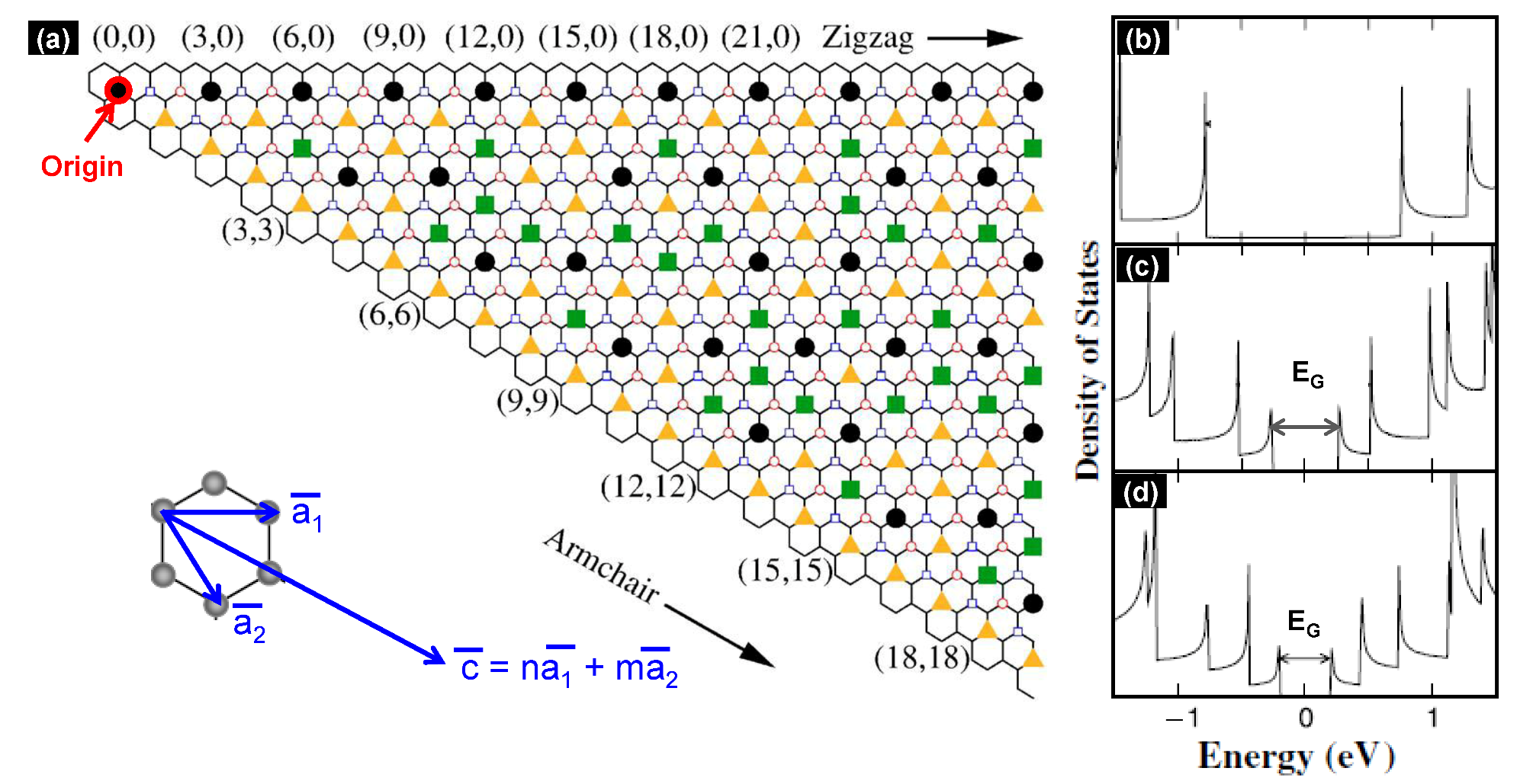
(Figure 1a), aC-C = 0.142 nm is the C–C bond length, t ~ −3 eV is the C–C bonding energy. SWCNTs with n = m are called armchair nanotubes and always show metallic behavior, whereas SWCNTs with nm either show metallic behavior for mod (nm)/3 = 0 or semiconducting behavior for mod (nm)/3 = 1, 2. SWCNTs with m = 0 are called zigzag nanotubes and the rest with nm ≠ 0 are called chiral nanotubes.
Semiconducting SWCNTs (s-SWCNTs) are of particular interest for future electronic devices, where s-SWCNTs act as a channel in conventional field effect transistor (FET) configuration. Carrier mobility in such s-SWCNT-FETs can be as high as ~105 cm2/V-s [5,6], which outperforms similar values in current-day FETs. In addition, the ultra-thin s-SWCNT layer that forms the channel of FET offers better electrostatic gate control, hence less short channel effect compared to classical silicon-based FETs [7]. Such ultra-thin layers also offer extreme mechanical flexibility to the resultant electronic device, thereby promoting the best platform for future flexible electronic devices [8,9], which are currently being manufactured using FETs made on thin silicon substrates [10,11]. Use of s-SWCNTs as channels, m-SWCNTs as contacts [12] and memory elements [13], SWCNT network [14,15] or single s-SWCNT [16,17] as memory, and CNT fabrics as coaxial cable [18] may open up the possibility of having “all-CNT” electronics for high performance applications. In addition to electronics, SWCNT-FETs are also considered as chemical-/bio-sensors because of their higher surface-to-volume ratio that reduces response time [19] and extreme sensitivity [20,21], and their selectivity [20] to chemical and biological species.
To enable all these applications stated in the last paragraph, SWCNT-FETs and memories not only require superior performance, but also require a controlled level of variability and reliability. Such controllability has to ensure that performance of associated devices does not drop below a certain limit, which can be compensated through circuit design via guard bands [22,23]. Figure 2 schematically explains the extent of guard band that is used in circuit design for handling variability and reliability. Devices have different variability sources that give rise to time-zero variation in device performance around its mean value. In addition, during the operation of the device, its performance degrades over time and such degradation comes with its own statistical variation. Based on this knowledge, circuits are designed with such devices considering that the tail of the performance distribution at the end of intended lifetime will not go beyond a certain limit—thus, the designed circuits are guard-banded against performance variations. As device performance improves via Moore’s law scaling [24], device design is continuously modified to minimize guard-band such that the devices can be operated at higher performance without compromising the lifetime.
Figure 1. (a) Two-dimensional graphene lattice for defining structures of (n,m) Single-Walled Carbon NanoTubes (SWCNTs) (reprinted with permission from Ref. [3]; © 2005 by the American Physical Society.). Definition of lattice vectors a1, a2 with respect to carbon atoms in the graphene lattice is shown in the bottom part of the figure. SWCNTs can be formed by rolling this sheet to join the origin (a1,a2) = (0,0) with other points. Joining the open symbols with the origin makes semiconducting SWCNTs, while joining the solid symbols with the origin makes metallic SWCNTs. (b) Density of states (DOS) vs. energy plot obtained using a tight binding model [4] for an armchair (10, 10) SWCNT having metallic property. (c,d) DOS + energy plot for a chiral (11, 9) SWCNT and a zigzag (22, 0) SWCNT. Both these SWCNTs have semiconducting properties and a chirality-dependent band gap (EG) defined using Equation (1). (bd) are reprinted with permission from Ref. [4]; © 2003 IOP Publishing Ltd and Deutsche Physikalische Gesellschaft, Published under a CC BY-NC-SA license.
Electronics 02 00332 g001
In this review article, we will discuss different aspects of variability and reliability in SWCNT-FETs that will eventually define guard-band in such devices. Section 2 discusses the configurations and performance of SWCNT-FETs that has potential use in future electronics. Section 3 highlights the sources of variability in SWCNT-FETs and the current solutions to control them. Section 4 performs a similar review for the reliability sources. Section 5 summarizes the paper and provides brief guidelines for improving variability and reliability phenomena in SWCNT-FETs based on current understanding of CNT growth conditions and device fabrication challenges.
Figure 2. Schematic representation of the amount of guard-band that is used in electronics for handling process (or time-zero) variation and reliability (time dependent variation) in device performance. The performance of a device has a distribution over and above its mean value and it degrades over time. Once of the tail of performance distribution for the device reaches the guard-band margin, the associated device is designed to fail.
Electronics 02 00332 g002

2. Configurations and Performance of SWCNT-FET

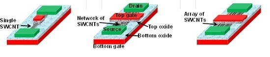
2.1. Device Geometry

For FET applications, SWCNTs are commonly grown in random networks or aligned arrays using metal catalyst placed on SiO2 [9,12,25,26]. Alternately, SWCNTs are drop-casted from solution on SiO2 [27,28,29] or hafnium dioxide (HfO2) [30,31] and assembled in random networks [27,28,29] or parallel arrays [31,32] via coating of self-assembled monolayers on oxides. Bottom-gated FETs with thick SiO2 as gate dielectric and heavily doped silicon as gate are widely used test configurations for SWCNT-FETs. Such bottom-gated structures though are suitable for bio-/chemical-sensing applications [20,21,33], top-gated geometry with thin, high-κ gate dielectric is preferred for high performance electronics [34,35]. (In some novel SWCNT-FETs, local bottom-gating [36], lateral gating with suspended SWCNTs [37], and surround-gate geometries [38] are also used for high performance electronics.) Measurement of SWCNT properties (e.g., conductivity, mobility, contact resistance of individual SWCNTs and their diameter dependence) by applying suitable bias at source, drain, and gate terminals involves fabrication of single SWCNT-FET. Schematic of such a FET in dual-gate (i.e., having top and bottom gate with suitable gate oxides) configuration is shown in Figure 3a. Such single SWCNT-FET, however, cannot provide the amount of current required for different applications, e.g., ~mA per µm of channel width is required for high performance electronics [35]. Current in SWCNT-FETs can be increased either by having a network (Figure 3b) or an aligned array (Figure 3c) of SWCNTs’ bridging sources and drain terminals. Magnitude of current in these configurations depends on the density of SWCNTs (per unit area for network SWCNTs of Figure 3b or per unit width across the length of SWCNTs for aligned SWCNTs of Figure 3c), diameter of SWCNTs, chirality of SWCNTs, and electrostatic coupling on SWCNTs via gate. For network SWCNT-FETs, current additionally depends on the charge transfer efficiency across different SWCNTs in the network [39,40,41].
Figure 3. Schematic representation of SWCNT-based field effect transistor (FETs) in top- and bottom-gated configuration for (a) single SWCNT, (b) SWCNT networks, and (c) aligned array SWCNTs. Generally, SWCNTs are grown or coated on oxides and then the source, drain, top oxide and top gate are formed on top of them via lithography. Though the schematics here show partial coverage of SWCNTs in between source and drain, the actual top-gate SWCNT-FET application uses full coverage of SWCNTs.
Electronics 02 00332 g003

2.2. Materials for SWCNT-FETs

As mentioned before, SWCNTs are grown on insulating substrates like SiO2, quartz, sapphire, etc. using metal (e.g., Fe, Ni, Co and their alloys) nanoparticles as catalyst. Length, diameter distribution, and chirality of grown SWCNTs vary among the growth methods being used [42,43]. In general, for as-grown SWCNTs, length varies from ~1 µm to several 100 µm, diameter ranges between ~0.7 nm and ~5 nm [26,44,45,46], density is approximately 14–200 per μm2 for network SWCNTs [12,31] and ~2–45 per µm across the length of the SWCNT for aligned SWCNTs [26,31,44,47,48], and chirality varies randomly. Long SWCNTs (>100 µm) are only obtained during chemical vapor deposition (CVD) on stable temperature- (ST-) cut quartz substrates [25,49]. Diameter and chirality of as-grown SWCNTs can be sorted by dissolving SWCNTs in surfactants and then using post-processing techniques like ultra-centrifugation [50], gel electrophoresis [51], chromatography [52]. Such solution-processed, sorted SWCNTs can be assembled into a high-density compact film via Langmuir-Blodgett method [35]. However, solution-processing breaks SWCNTs into small segments (~µm or less) and reduces the carrier mobility or conductivity of SWCNTs (down to ~1–20 cm2/V-sec [35,46] with a maximum of ~200–300 cm2/V-sec [28,53]). An alternative approach of maintaining the integrity of SWCNTs in terms of length (up to several hundreds of µm) and carrier mobility (>1000 cm2/V-sec) is to coat horizontally aligned SWCNTs with a molecular film and use thermo-lithography (thermal analogous of photo-lithography) to etch-off m-SWCNTs from the substrate [54]. Remaining s-SWCNTs have a low density; however, there is potential for density improvement via multiple transfers [55,56].
In addition to the requirement of having substrates with high density s-SWCNTs, future electronic devices require appropriate doping in s-SWCNTs to control their conduction. Absence of molecular doping in SWCNTs, however, necessitates the use of metals with lower (higher) work-functions to conduct electrons (holes) through the SWCNTs, hence make n- (p-) type SWCNT-FETs. Palladium (Pd) with work-function of ~5.1 eV is generally used as source/drain contacts for making p-type SWCNT-FETs that allows hole flow from contacts into and out of the SWCNT via Schottky contacts for d < 1 nm SWCNTs and via ohmic contact for d > 1 nm SWCNTs [57,58,59]. Presence of negatively charged hydroxyl (-OH) groups at SWCNTs interface also makes the p-type conduction in SWCNT-FETs easier. N-type or electron conduction in SWCNTs, on the other hand, can be enabled using calcium (Ca) and scandium (Sc) source/drain contacts with work-functions ~3–4 eV [60,61]. In such case, conduction can be further enhanced via electrostatic doping with high-κ oxides [38,62].

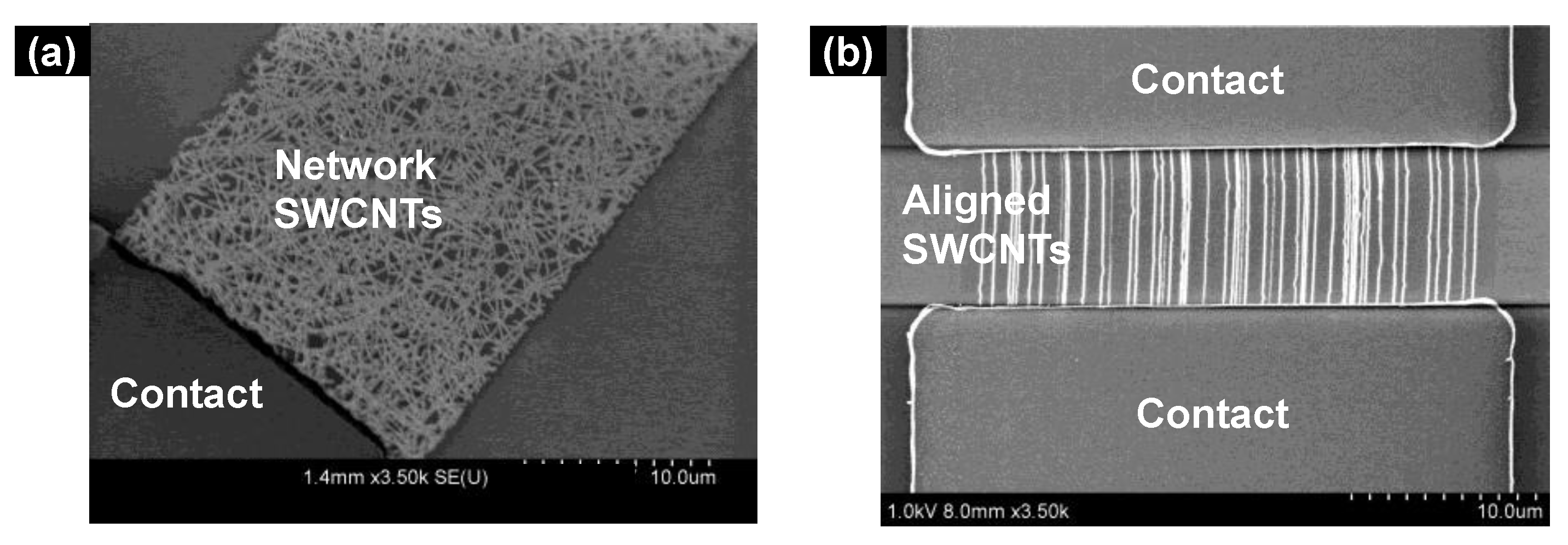
2.3. FETs with Single SWCNT

Current-voltage (I-V) characteristics of FETs with single s-SWCNT have reasonably good switching behavior in the measured transfer characteristics (i.e., drain current (Ids) vs. gate voltage (Vg) characteristics, as shown in Figure 4a) and good saturation in output characteristics (i.e., Ids vs. drain to source voltage (Vds) characteristics, as shown in Figure 4b) for any channel length (Lch) down to ~10 nm [63]. These FETs have predominant p-type behavior because of the natural presence of –OH groups at the interface of SWCNTs. On-current (Ion; defined as Ids at a certain high |VgVt|, where Vt is the threshold voltage of a FET) and off-current (Ioff; defined as the minimum of Ids) in these FETs with single s-SWCNT show variation with d and source/drain contact material being used. Contacts with higher work-function (ΦWF) can inject holes into the valence bands of s-SWCNTs more easily and have larger Ion and Ioff (Figure 4c,d); [44,58,59]), especially for larger diameter s-SWCNTs that have smaller band-gap, Eg (see Equation (1)) and hence have negligible hole injection barrier at the metal/s-SWCNT interface. Therefore, contacts play a major role in the conduction of SWCNT-FETs and are considered to have dominant contribution in limiting Ids in the near ballistic limit [28,63], when Lch is much less than the channel mean free path that defines mobility. Sub-threshold slope (SS; defined as ∂Vg/∂(log10Ids) in the region with Vg << Vt) for FETs with single s-SWCNT varies from ~80–95 mV/dec and increases with a decrease in Lch due to ambipolar conduction [64]. (Use of appropriate chemical coating on SWCNT in a dual-gate device configuration can reduce SS to 63 mV/dec [65], which is close to the theoretical limit of SS = 2.3kBT/q ~ 60 mV/dec at room temperature for a FET [66]; here, kB is the Boltzmann constant, T is temperature in °K, and q is the electron charge.) Hole effective mobility (μeff,h) of s-SWNTs ranges from ~103–105 cm2/V-sec [5,6,25,63,67] and increases with d [5]. Such μeff,h value depends on CNT growth conditions and is better for CVD-grown CNTs compared to solution-processed CNTs [28].
In contrary to s-SWNTs, FETs with single metallic (m-) SWCNT-FETs have very small gate modulation and show ambipolar behavior with a smaller n-type tail (Figure 5a). Such gate modulation is often attributed to the presence of Mott-insulating states [68] and/or strain-induced bandgap [69] in m-SWCNTs. FETs with s-SWCNTs also show ambipolar behavior, more significantly at higher |VDS| and for larger diameter s-SWCNTs (Figure 5b) due to band-to-band tunneling (BTBT) [70].

2.4. FETs with Multiple SWCNTs

Multiple SWCNTs in FET’s channel are either arranged randomly as network or aligned parallel to each other bridging source and drain. Network SWCNT-FETs can be made using CVD-grown SWCNTs with mixed chiralities (Figure 6a shows a scanning electron microscope (SEM) image for one such bottom-gated FET near a source/drain contact). These FETs have low on/off ratio, unless the conduction through metallic SWCNTs is turned off via periodic stripping [9]. An alternate way of improving on/off ratio is to use solution-processed, chirality sorted s-SWCNTs for making FETs. However, such FETs show lower conductance compared to CVD-grown SWCNTs because of the presence of structural defects [28].
Figure 4. (a) Transfer or Ids-Vg and (b) output or Ids-Vds characteristics of single s-SWCNT-FETs (reprinted by permission from Macmillan Publishers Ltd: Nature Nanotechnology [63], © 2010). Diameter dependence of (c) on-current Ion and (d) off-current Ioff for s-SWCNT-FETs using different types of metals (palladium: Pd, copper: Cu, titanium: Ti) as source/drain (reprinted with permission from Ref. [58], © 2006 American Chemical Society.). In general, easier hole conduction for higher work-function (ΦWF) contact metals like Pd results higher Ion and Ioff for associated FETs.
Electronics 02 00332 g004
Network SWCNTs have impedances at the junctions of different SWCNTs; consequently, they have lower conductance and are suitable only for applications like non-volatile memories [14,15]. Parallel arrangement of aligned SWCNTs resolves the issue with junction impedance and promises applications of SWCNTs in high performance radio frequency (RF) electronics [47,71,72], and transparent electronics [73,74]. Figure 6b shows a SEM image of one such top-gated FET before gate dielectric and gate metal formation. These aligned array SWCNT-FETs are either fabricated by growing SWCNTs via CVD on special types of quartz or sapphire substrates, whose crystal orientations [49] and/or step-edges [75,76] help parallel alignment (with less than 0.1% imperfection [77]) of d ~ 0.7~3 nm SWCNTs [26,44,45], or fabricated by aligning solution-processed SWCNTs via dielectrophoresis [46]. CVD-grown SWCNTs are long (with a length of several hundreds of µm [77]) and have high conductivity [5,25,63,67], however, require the use of post-processing techniques like thermo-lithography [54] and laser irradiation [78] for removal of m-SWNTs, or electrical breakdown [79] for breaking the continuity of m-SWNTs, and hence, cause FETs to use the remaining s-SWNTs.
Figure 5. (a) Transfer characteristics of single metallic (m-) SWCNT-FETs showing ambipolar behavior (reprinted with permission from Ref. [44]; © 2012, AIP Publishing LLC). (b) Ambipolar behavior is also observed for FETs with a d ~ 1.7 nm s-SWCNT and at larger Vds (reprinted with permission from Macmillan Publishers Ltd: Nature Nanotechnology [54], © 2013).
Electronics 02 00332 g005
Figure 6. Scanning electron micrograph (SEM) of (a) random network of SWCNTs near one of the source/drain contact and (b) horizontally aligned SWCNTs bridging source/drain contacts.
Electronics 02 00332 g006

3. Variability in SWCNT-FETs

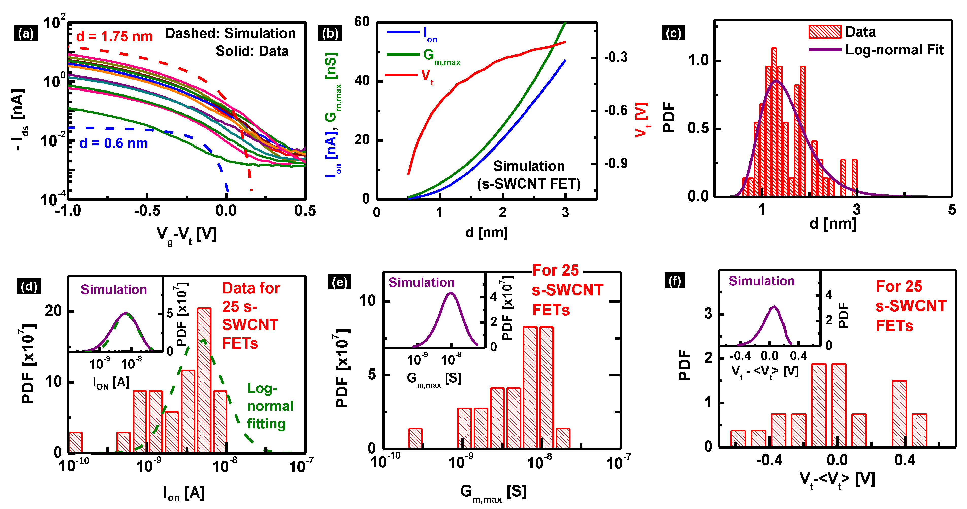
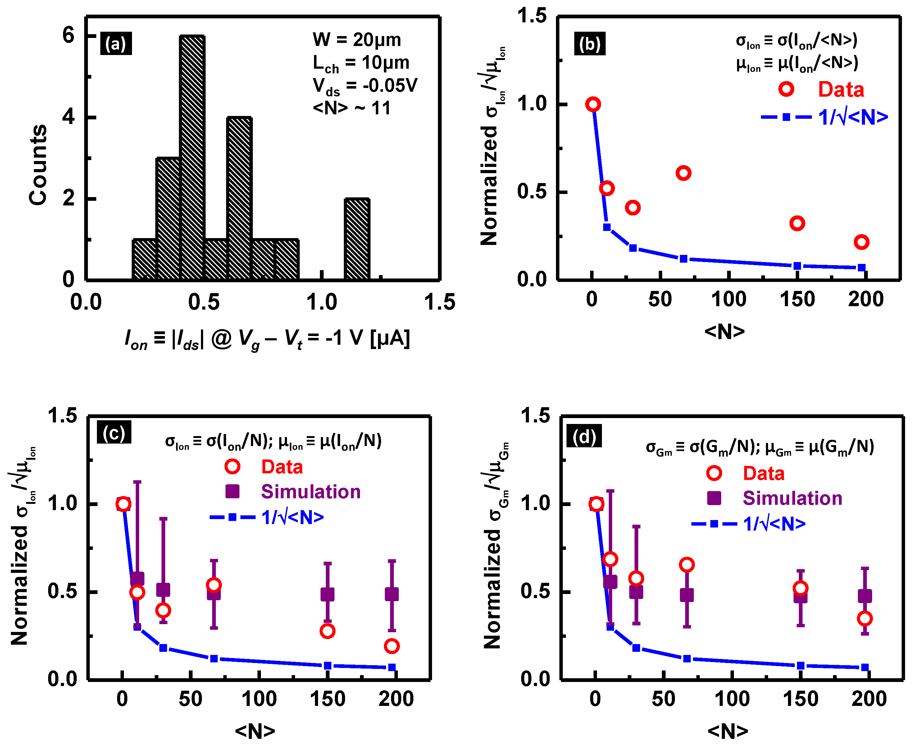
3.1. Variability in FETs with Single SWCNT

Performance variation in FETs with single s-SWCNT arises from the variation in d, contact and gate metals’ ΦWF, Lch, Tox (oxide thickness), and interface and oxide defects from one FET to another. For FETs with Lch>µm, variation in d can give rise to several orders of magnitude change in Ids, as shown in Figure 7a for small Vds = −50 mV. One can simulate such transfer characteristics for different d (dashed lines in Figure 7a) by considering the conductance of the FET (Gds) as a series combination of conductances of s-SWCNT (Gss; see Ref. [44] for appropriate expressions) and contact (Gc = Gc0Tc; where Tc is the transmission probability of carriers near the source/drain contact) with components from both electron (e) and hole (h), i.e.,
Electronics 02 00332 i002
and hence, calculate Ids using Ids = Gds × Vds. Simulated results for 0.6 nm < d < 1.75 nm are consistent with measurement at Vg < Vt, where Gss dominates Gds. The differences in the region of Vg > Vt, where Gc dominates Gds, partly reflect variation in the fixed component of Gc [80] that is not considered in simulation and also reflect Ids measurement limitation set at ~pA. Plots of diameter dependence of Ion (≡Ids @ VgVt = −1V, Vds = 50 mV), maximum transconductance Gm,max (≡max |∂Ids/∂Vg|), and Vt (Figure 7b) provide additional detail about the origin of performance variation in s-SWCNT FET. At large diameters, when the transmission of carriers through the Schottky barrier near the contacts is unity, variation of Ion ~ d and Gm,max ~ d2 originates from the diameter dependence of μeff in s-SWNTs [5,81,82]. Similarly, variation of Vt (≡Vg @ |Ids| = |Ids,max|/100) with d follows that of Ion. At small diameters, non-linear dependence of transmission through the contact Schottky barrier leads to a non-linear variation in Ion, Gm,max, and Vt with d.
Simulated Ion, Gm,max, and Vt distributions (calculated using diameter distribution of Figure 7c and variations of Ion, Gm,max, and Vt vs. d from Figure 7b) suggest good consistency with respective measurements (Figure 7d–f). Similar to the diameter distribution of Figure 7c, Ion distribution fits log-normal statistics, except near the lower tails of the distribution where transport through the contacts’ Schottky barrier with Tc < 1 dominates Ids. Measured Vt − <Vt> distribution (where <Vt> is the average of the distribution) is wider than the simulated one due to the extra contributions from defects [16,83] and gate ΦWF [84,85] variations that is not considered in the simulation. Passivation of SWCNT interface using hydrophobic self-assembled monolayers (SAMs) can tighten the Vt distribution by reducing hydroxyl (–OH) group related interface defects [86]. Figure 8a demonstrates utility of such SAM-based approach for reducing Vt distribution, where Lch << µm s-SWCNT FETs are made using solution-processed SWCNTs and passivated with hexamethyldisilazane (HMDS). As in CVD-grown s-SWCNTs, distribution in Gm (Figure 8b) for such solution-processed s-SWCNT FETs follows that of diameter (Figure 8c). In addition, contact resistance Rc = 1/Gc in such small Lch s-SWCNT FETs plays a dominant role in transport. Distribution of Rc (Figure 8d) arises from variations in Tc with d [28] and also from variations in the contact’s ΦWF. In contrary, FETs with m-SWCNT and similar Lch have tighter Rc distribution [28]; however, they still suffer from variations in Ids (Figure 8e) and, hence, Gm (Figure 8f). Since m-SWCNTs are unattractive for high performance electronics applications requiring high Ion/Ioff, parametric variations in m-SWCNT FETs are not well studied.

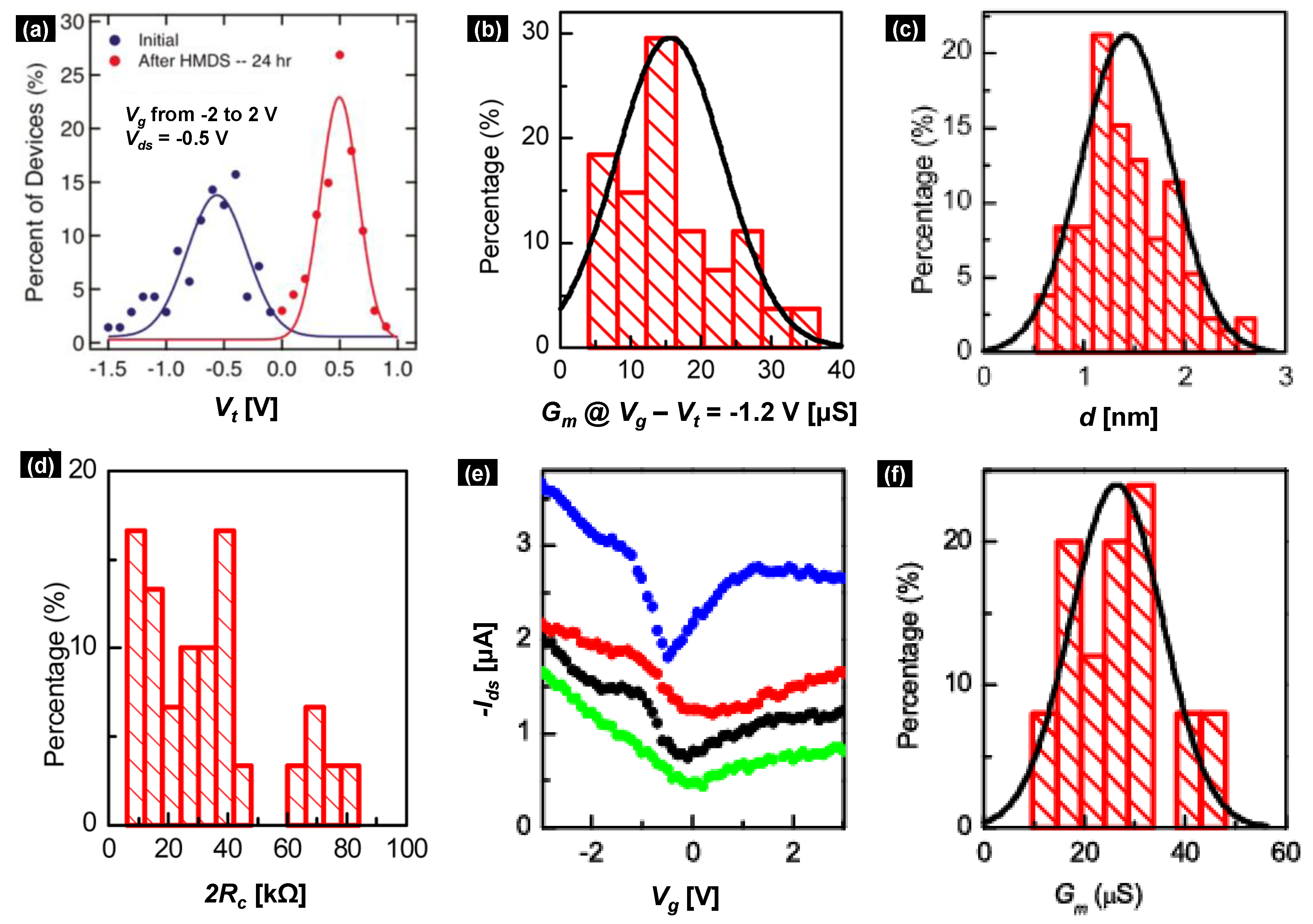
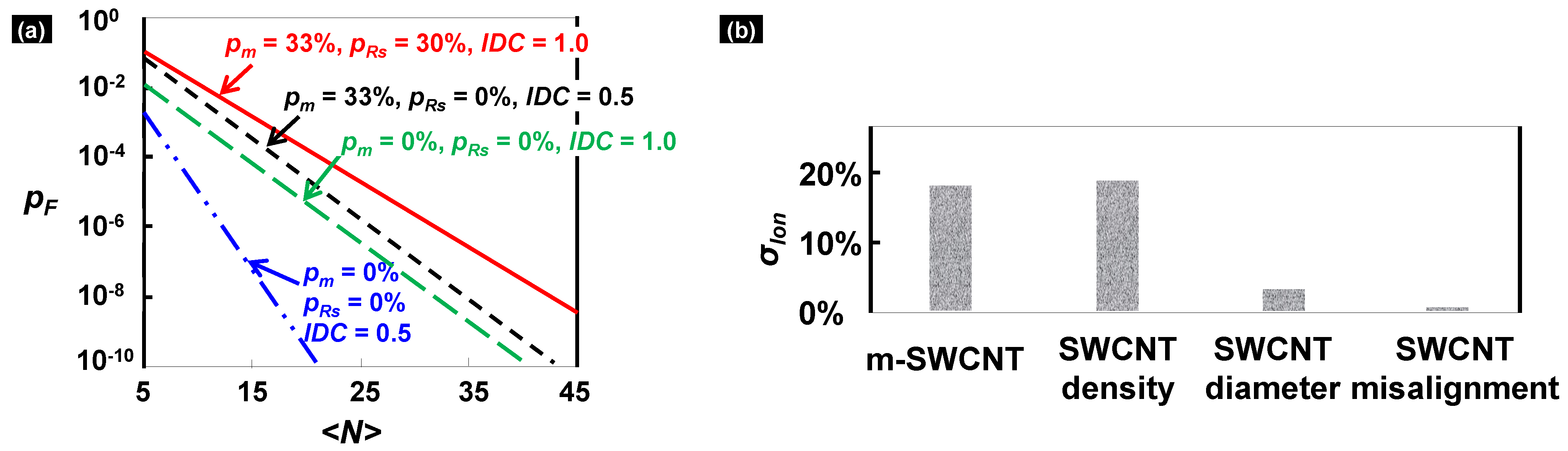
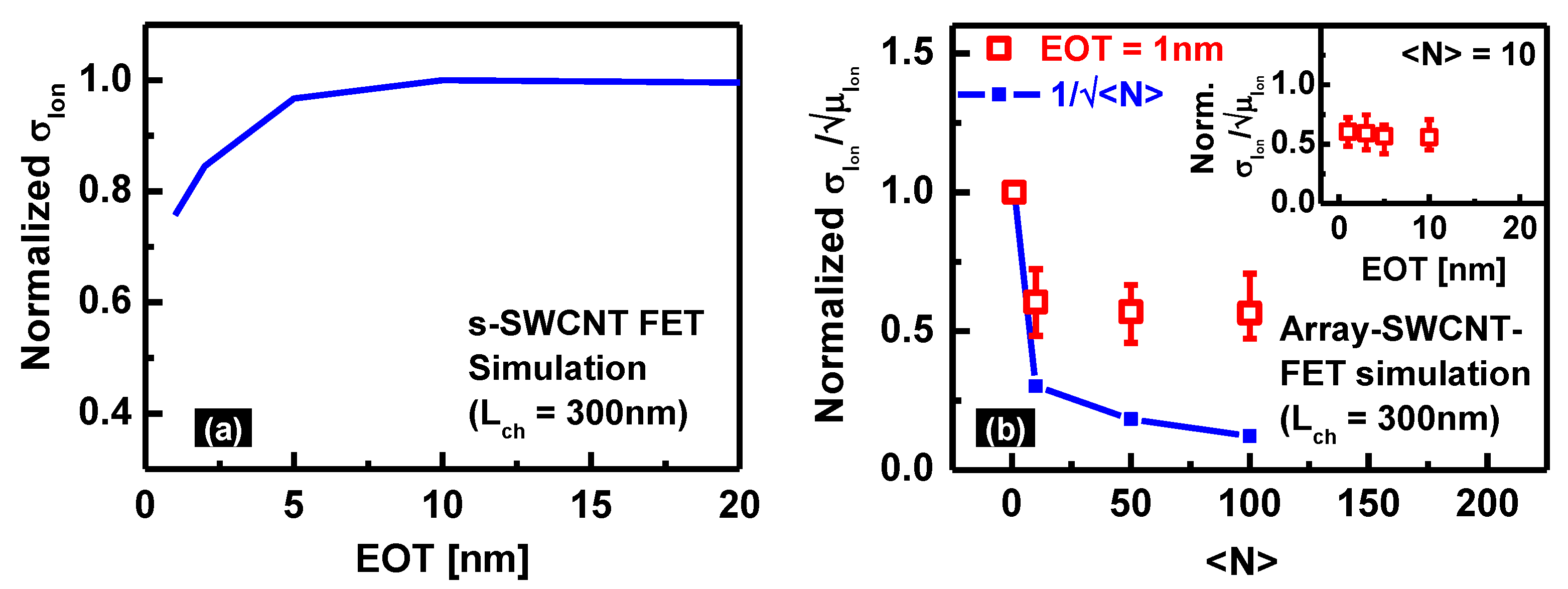
3.2. Variability in FETs with Multiple SWCNTs

Similar to single SWCNT-FETs, performance variation in FETs with multiple SWCNTs originates from variations in d, ΦWF, Lch, Tox, and defects [87,88,89]. A simple translation of single SWCNT-FET analysis to multiple SWCNT-FET; however, they cannot explain related variations, mostly because of the added complexity coming from variations in the arrangements and types of multiple SWCNTs bridging source/drain contacts. Multiple SWCNT FETs can have random network or aligned SWCNTs with varied density of m- and s-SWCNTs, a wide range of variations in the orientation of SWCNT and its crossings (especially for network SWCNT FET), and a wide distribution in d. This section discusses performance variation in aligned array SWCNT-FETs that have significant promise for high performance device applications. Such FETs have negligible variation in SWCNT’s orientation [77] and also have negligible SWCNT crossings (Figure 6b). For a discussion on variabilities coming from SWCNT’s orientation and crossings, which are more relevant for network SWCNT-FETs, please refer to Ref. [41].
Figure 7. (a) Measured Ids vs. VgVt (VtVg @ |Ids| = |Ids,max|/100) characteristics for single s-SWCNT FETs (Lch ~ 10 μm, Vds = −50 mV) is within the simulated results for d = 0.6 nm and d = 1.75nm FETs. (b) Simulated Ion (≡|Ids|@ VgVt = −1 V, Vds = −50 mV), Gm,max (≡max(∂Ids/∂Vg)), and Vt vs. d for s-SWCNT FETs. (c) Diameter distribution that is used to simulate performance distributions of s-SWCNT FETs in (df). Measured distributions of (d) Ion, (e) Gm,max, and (f) Vt for s-SWCNT FETs agree well with the simulated distributions (insets). For (f), <Vt> is the average of Vt distribution. These figures are reprinted with permission from Ref. [44]; © 2012, AIP Publishing LLC.
Electronics 02 00332 g007
Solution-processed SWCNTs that are widely used for fabrication of FETs with network and partially aligned SWCNTs have yet to reach the target of 100% chiral selectivity. Some of the resultant FETs, therefore, have high on/off ratios when SWCNT density within the FET is low [35,46]. On the other hand, high performance electronics demand the availability of CVD-grown SWCNTs that always come with a mixture of m- and s-SWCNTs and require the application of post-processing techniques (e.g., electrical breakdown [79], gas-phase reaction [90], thermo-lithography [54]) for having high on/off ratio in multiple SWCNT FETs. In some cases, application of post-processing techniques like electrical breakdown [79] and gas-phase reaction [90] also leads to unwanted removal of s-SWCNTs and, hence, performance degradation or even transistor failure [91]. Considering pm as the probability of a single SWCNT in the FET being metallic, pRs as the probability of s-SWCNT being removed via post-processing, IDC as the index of dispersion in SWCNT count within the FET, one can simulate the failure probability (pF) for FETs with aligned SWCNTs at different SWCNT densities (Figure 9a). Such analysis, however, ignores a well-known aspect of ‘inferential statistics’ [92], i.e., the distributions of SWCNT density and d in macro-scale (population distributions) is not always same as the distributions in micro-scale (sample distributions). As such, performance variability from diameter variations were expected to diminish for high density multiple SWCNT FETs via statistical averaging [25,41,91], making SWCNT density and m-SWCNT’s presence as the major contributors to performance variations (Figure 9b) [91].
Figure 8. (a) Treatment of hexamethyldisilazane (HMDS) for 24 h narrows the Vt distribution significantly. Vg was swept from −2 V to 2 V for p-type, solution-processed s-SWCNT FETs during this measurement. Measured (b) Gm distribution and (c) diameter distribution for similar solution-processed, s-SWCNT FETs that has small channel length (Lch = 150 nm). (d) Extracted contact resistance (Rc) distribution for Lch = 150 nm, solution-processed s-SWCNT FETs. (e) Transfer characteristics and (f) Gm distribution for solution-processed, m-SWCNT FETs. (ac) and (df) are reprinted with permission from Refs. [28] and [86], respectively; © 2012 American Chemical Society.
Electronics 02 00332 g008
We performed a comprehensive experimental and theoretical study on FETs with aligned array SWCNTs [44] and ruled out the presence of statistical averaging in aligned-array SWCNT-FETs. Figure 10a plots distribution of Ion (measured at a Vg − Vt = −1 V) for aligned array-SWCNT FETs having <N> ~ 11 SWCNTs, where <N> = <ρ>W is nominal number of SWCNT within the FET, W is the channel width, and <ρ> is the average SWCNT density on the substrate per µm across the length of the nanotubes. Since variation in Ion follows Poisson statistics [44], we account for changes in µIon (that arises from variation in sample preparation) from one set of array-SWCNT FET to another by dividing the standard deviation of Ion/<N> (σIon) with √µIon (where µIon is the average of Ion/<N>). Calculated σIon/√µIon, normalized with respect to the same value measured for FETs with single SWCNT, shows a small reduction with the increase in <N> (Figure 10b). If the diameter and density distributions of SWCNT for each array-SWCNT FETs (sample distribution) were the same as the wafer-level distribution (population distribution) of these parameters, as per central limit theorem [92], the normalized standard deviation should have reduced as 1/√<N> due to statistical averaging. The existence of deviation from 1/√<N>, therefore, suggests significant variations in SWCNTs’ density and diameter across the wafer, as was confirmed via extensive atomic force microscopy (AFM) at different locations over a macroscopic area of ST-cut quartz substrate that had CVD-grown aligned arrays of SWCNTs [44].
Figure 9. (a) Variation in failure probability (pF; defined as probability of having no s-SWCNT within the FET) of m-SWCNT removed (via post-processing) aligned-array SWCNT-FETs with <N> (defined as the average number of SWCNTs within the FET before post-processing). Simulation is performed for different values of pm (defined as the probability of having m-SWCNT within the FET before post-processing), pRs (defined as the probability of s-SWCNT removal via post-processing), and IDC (index of dispersion in SWCNT count). (b) Different variation sources like the presence of m-SWCNT before post-processing, SWCNTs’ density, diameter, and misalignment contributes differently to the overall variation in standard deviation of Ion (σIon). Simulation suggests that the presence of m-SWCNT and density distribution are the key variability sources in SWCNT FETs. These figures are plotted using data from Ref. [91].
Electronics 02 00332 g009
To clarify the differences between measured σIon/√µIon and expected 1/√<N> dependency, measured diameter and density variations across the wafer are used first to calibrate the variations measured at the microscopic level (i.e., electronic properties of single-SWNT-FETs, as discussed in section 3.1). Later, the rules of “inferential statistics” [92] is used to analyze variations at the macroscopic level (i.e., for array SWCNT FETs). Here, density variation is eliminated by counting the number of SWCNTs (N) for each array-SWNT FET and then using (Ids/N) − Vg characteristics for standard deviation calculation. Even after accounting for density variation, calculated σIon at different <N> (normalized to its value for <N> = 1) shows significant deviation from 1/√<N> scaling (Figure 10c). Such deviation suggests SWCNT density variation as a minor contributor to performance variation, thus contradicting the results of Refs. [25,41,91]. Finally, Ids-Vg characteristics of array-SWCNT FETs are simulated for different <N> by considering experimentally calibrated diameter dependence of single-SWCNT FETs’s Ids-Vg characteristics (Figure 7a) and measured (wafer-scale) density, diameter distributions of SWCNT. Figure 10c,d show normalized standard deviations of Ion (σIon) and Gm,max (σGm), as simulated for different <N> and their comparison to measured quantities. Since the sample sizes in measuring the standard deviations were small (~17–35), simulated standard deviations show a range of magnitudes for similar sample sizes within which the measured data points fits in. (The simulation framework [44], used for calculating σIon and σGm of array-SWCNT FETs, neglects contributions from m-SWCNTs. However, the procedure is suitable for demonstrating the importance of wafer-level variations in diameter and density).
Figure 10. (a) Distribution of Ion among array-SWCNT FETs with mean SWCNT density <N> ~ 11. (b) Normalized standard deviation of Ion (σIon) vs. <N> deviates from 1/√<N> scaling or central limit theorem. Normalized (c) σIon and (d) σGm for array-SWCNT FETs, where the effect of SWCNT density variation is removed by counting N for each FET and then calculating the standard deviations using Ids/NVg characteristics of each FET. Variations in σIon and σGm still differs from 1/√<N> and required the consideration of wafer-scale diameter distribution for matching experimental trends via detailed simulation. Figures are reprinted with permission from Ref. [44]; © 2012, AIP Publishing LLC.
Electronics 02 00332 g010
Recently, use of smaller equivalent oxide thickness (EOTεSiO2HKTox; where εSiO2, εHK are dielectric constants of SiO2 and high-κ dielectrics, respectively) has been shown to reduce the performance variation in FETs with single s-SWCNTs [93]. Decreasing EOT reduces the width of the Schottky barrier near the SWCNT and source/drain junction [57] and removes the long negative tails in the Ion distribution [44]. Moreover, as Lch approaches the carrier mean-free path of SWCNT, Ids saturates for large diameter SWCNTs and hence diameter dependence of Ids is less pronounced [44]. Both these effects are studied by simulating small-scale array-SWCNT-FETs with EOT ~ 1 nm and Lch = 300nm. (Here, simulated Ids-Vg [44] is calibrated with measurements of Ref. [63]). Simulation suggests a decrease in σIon for FETs with <N> = 1 with decreasing EOT (Figure 11a). However, at larger <N>, neither EOT nor Lch scaling could improve the statistics because the effects of variations in density and diameter remain significant (Figure 11b). Therefore, narrowing diameter and density distributions are identified as the main areas for improvement via advanced growth and/or purification techniques to reduce performance variation in multiple-SWCNT FETs.
Figure 11. (a) Oxide scaling of s-SWCNT FET reduces σIon (normalized by its value at equivalent oxide thickness (EOT = 20nm), as observed in Ref. [93]. (b) Normalized σIon (i.e., σIon/σIon,<N>=1) differs from 1/√<N> scaling for EOT = 1 nm array-SWNT FETs and show negligible effect of oxide scaling at fixed <N> (inset). Figures are reprinted with permission from Ref. [44]; © 2012, AIP Publishing LLC.
Electronics 02 00332 g011

4. Reliability of SWCNT-FETs

Reliability (i.e., device performance degradation) for any device can be interpreted by understanding its origin. For SWCNT-FETs, degradation arises from defects at the interface of SWCNT/oxide and also from defects within the oxide. Trapping and detrapping of carriers (i.e., electrons and holes) into and out of these defects changes performance parameters like Vt, Ids, Gm, etc. over time [94,95,96] and also causes hysteresis in the measured Ids-Vg characteristics [83]. In addition to these interface and oxide defects, performance of SWCNT-FET is also affected by topological or Stone-Wales defects [97,98]. They affect the transport of carriers through SWCNT; hence, they lower the mobility of associated FETs. On the other hand, controlled introduction of defects via UV/ozone/chemical treatment [99], doping [20,100], etc. enable the application of SWCNTs as sensors by providing low-energy adsorption sites for introduction of chemical species. These structural defects, however, do not evolve with time during the operation of SWCNT-FET, hence do not affect reliability.
In this section, we discuss the nature of interface (section 4.1) and oxide (section 4.2) defects in SWCNT-FETs and show how these defects raise reliability concerns such as hysteresis (section 4.3), low-frequency noise (section 4.4), radiation damage (section 4.5), and time-dependent performance degradation (section 4.6). These interface and oxide defects though cause reliability concerns at different quantities depending on the orientation and density of SWCNTs within the FET, the qualitative features of reliability remain the same for any orientation and density, as studied in context of hysteresis and performance degradation in Ref. [94]. Therefore, in contrary to Section 3, where variability of FETs with single and multiple SWCNTs is discussed separately, a general discussion of reliability without reference to SWCNTs’ density and orientation within the FET is sufficient for this section.

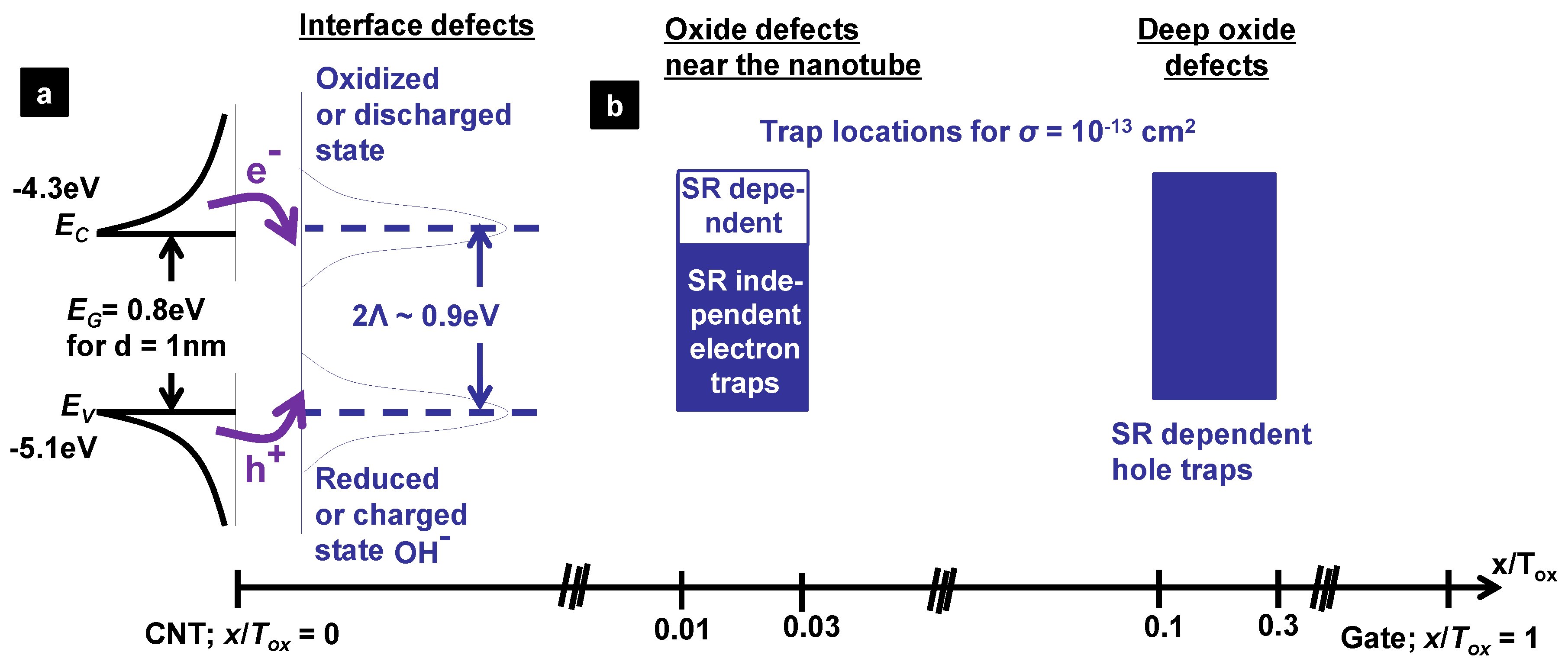
4.1. Interface Defects in SWCNT-FETs

Hydroxyl group (–OH), commonly present at any oxide surface [101,102], is the source of interface defects in SWCNT-FET [83,103,104]. Physisorbed water molecules and oxygen, present at the SWCNT/oxide in ambient condition, control –OH density [102] through electrochemical reaction: O2 + 4H+ + 4e ↔ 2H2O [102,105]. These –OH groups or interface defects surround SWCNTs laying on SiO2 surface (Figure 12a) and can give rise to large hysteresis in measured Ids-Vg characteristics [83,103,104], as well as potential time-dependent degradation in measured current [95,96]. Application of positive Vgs negatively charges –OH groups via electron capture from SWCNT positively shifts Vt and enhances hole conduction in commonly used p-type SWCNT-FET. Application of negative Vg, on the other hand, discharges the –OH group into neutral state, negatively shifts Vt and reduces hole conduction. Marcus-Garischer theory is generally used for modeling charging into or discharging from interface defects in SWCNT-FETs [94,105].
High temperature annealing under vacuum can reduce –OH groups [83,104] by eliminating water molecules at temperatures >190 °C [101]. Annealing at even higher temperature (at >1000 °C [101]) in vacuum would have completely removed the –OH groups; however, they have never been tested because of the high potential for damage to the SWCNTs and to the characterization system at such high temperatures. In addition to annealing in vacuum, –OH group or interface defects can also be reduced by using poly-methyl methacrylate (PMMA) encapsulation with thermal annealing [83] or by growing SWCNTs on different types of hydrophobic surfaces like octadecyltrichlorosilanated-SiO2 [103,106], hexamethyldisilazanized-SiO2 [86], octachlorotrisiloxane-capped organic dielectrics [107], etc.

4.2. Oxide Defects in SWCNT-FETs

Defects that are present within the gate dielectric, either near the SWCNTs or deep into the dielectric, also affect device performance. These oxide defects are broken bonds (Figure 12b) and pre-exist within the amorphous oxide network at various quantities, depending on the type of oxidation being performed. These pre-existing oxide defects can be annealed, for example, at high temperatures in hydrogen ambient [108]. Oxide defects are also generated near the vicinity of SWCNT during its growth, unless appropriate measures are taken to reduce the defects by running the growth in an inert environment [94]. In addition to the pre-existing ones, oxide defects are also generated during operation of FETs and causes dielectric breakdown [109,110,111]. The nature and origin of these oxide defects have been studied extensively using electron paramagnetic resonance [112,113], stress-induced leakage current [109], sweep-rate dependent Ids-Vg hysteresis [94], and optical excitation [114]. Unlike interface defects in SWCNT-FET, oxide defects are ambipolar and can either switch between negative and neutral charged states (i.e., act as electron traps) or switch between positive and neutral charged states (i.e., act as hole traps) [115]—thus, showing a wide range of reliability concerns as discussed below.
Figure 12. (a) Schematic representation of hydroxyl (–OH) group present at the surface of silicon dioxide on which SWCNTs are grown or placed. These –OH groups act as interface defect in SWCNT FETs. (b) Schematic representation of oxygen-vacancy related oxide defects [113] within silicon dioxide. (c) Transfer characteristics of s-SWCNT FET show large hysteresis between Vg sweeps performed in positive to negative and negative to positive directions. Measured hysteresis depends on sweep rate of Vg. (a,c) are reprinted with permission from Ref. [83]; © 2003 American Chemical Society.
Electronics 02 00332 g012

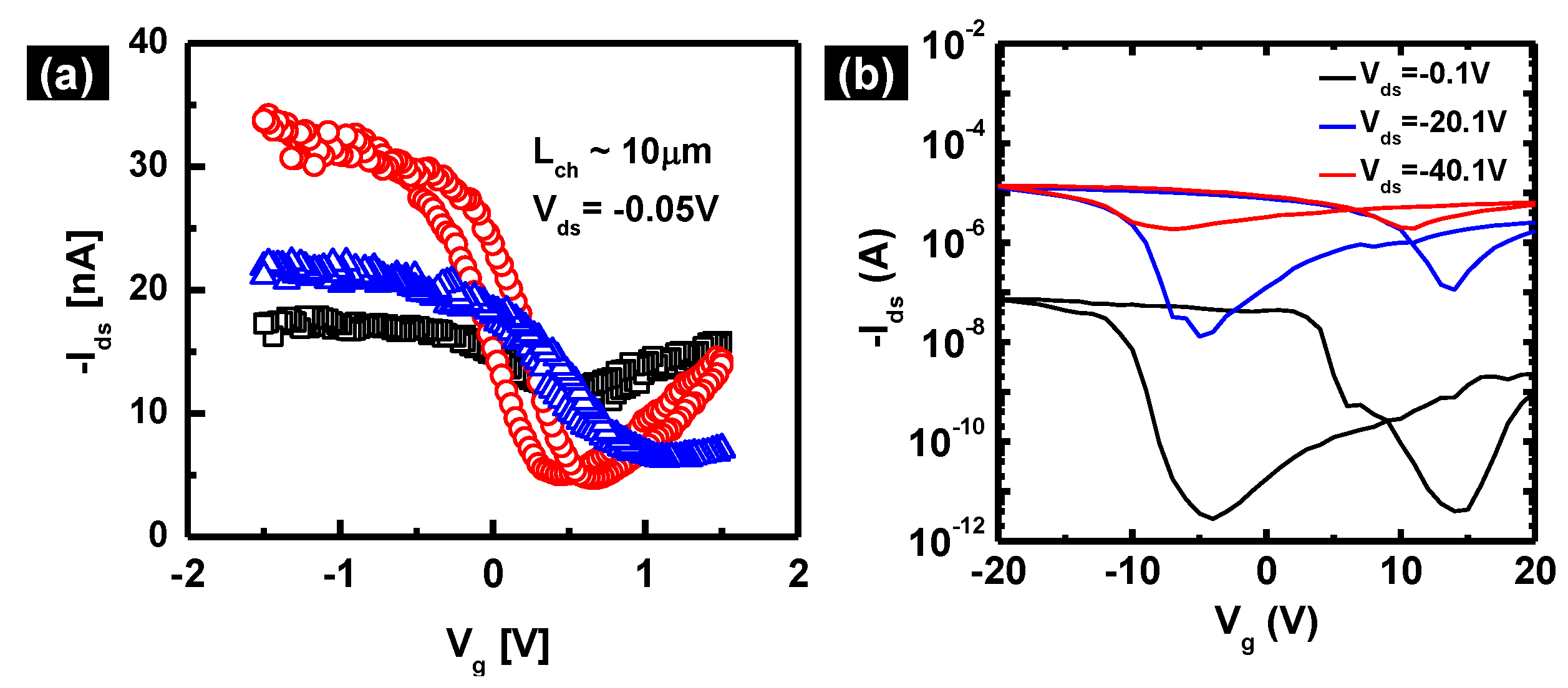
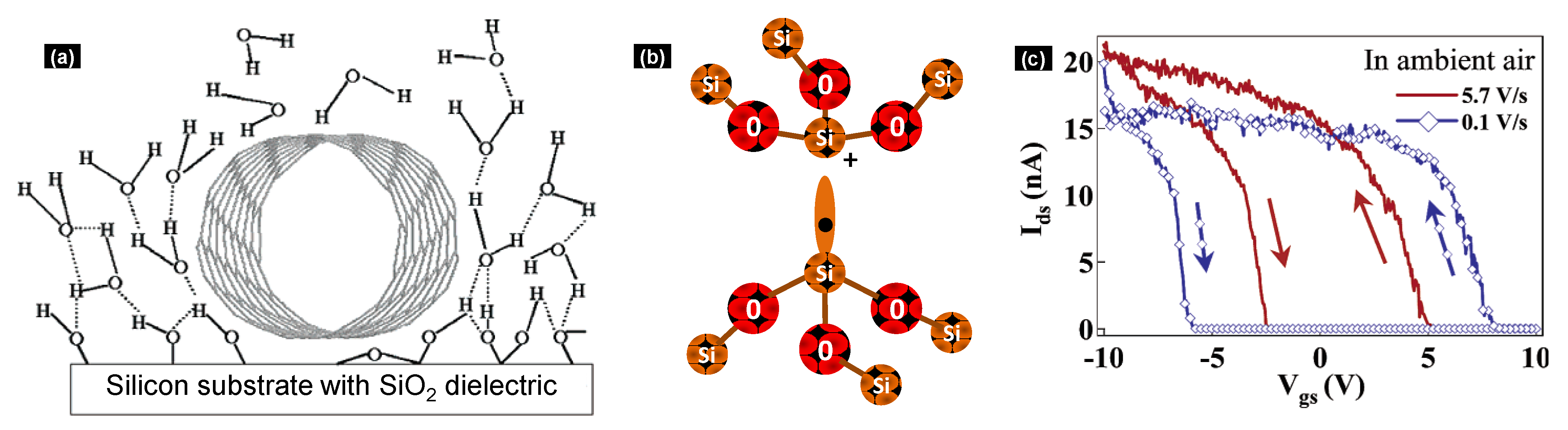
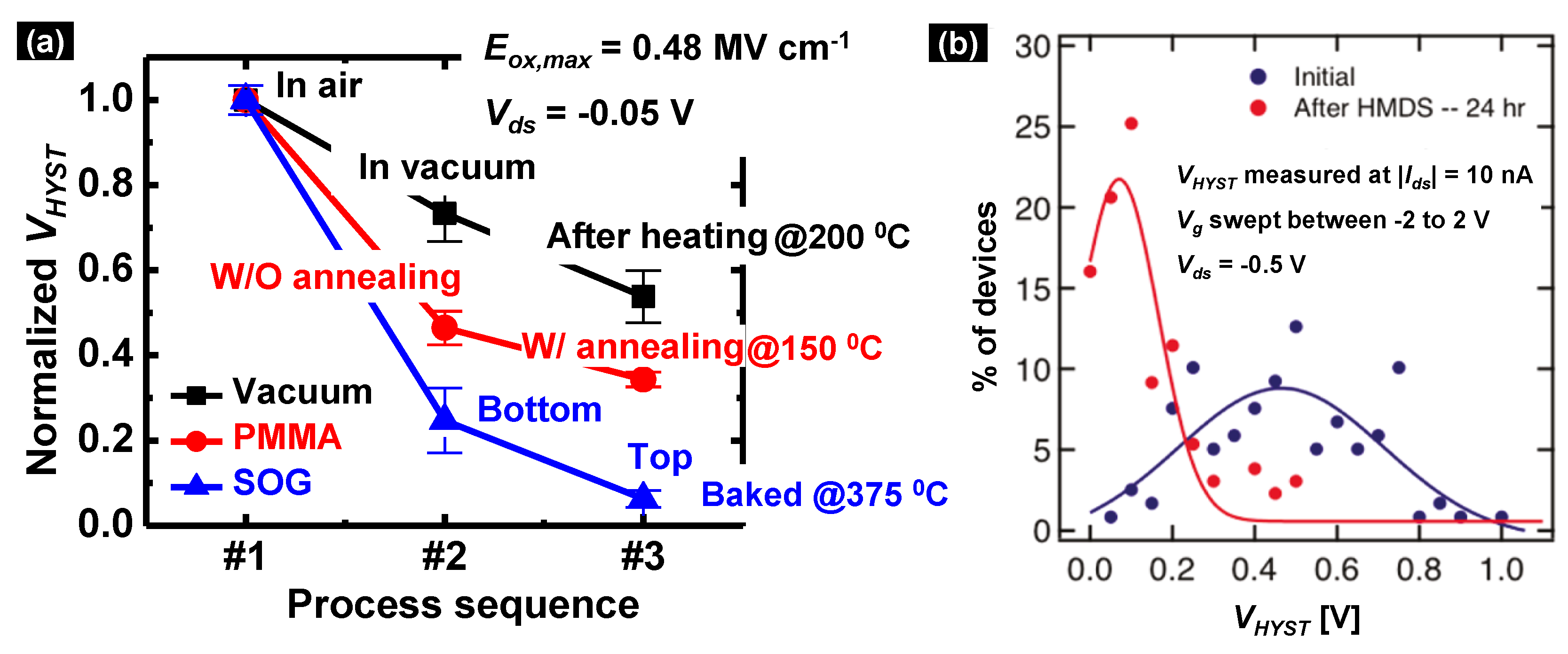
4.3. Hysteresis in SWCNT-FETs

Large hysteresis in Ids-Vg characteristics is a common phenomenon in SWCNT-FET and its magnitude depends on the concentration of defects in the FET [83,94], density of SWCNT [116], and also on the magnitude [94,107,117] and sweep-rate of Vg [83,94] (Figure 12c). Two stable charged and discharged states for the defects and switching between these states by application of appropriate Vg is the origin of hysteresis. Though such hysteresis promises memory applications using SWCNT, it is detrimental for device applications.
As mentioned before, both interface and oxide defects can give rise to hysteresis in SWCNT-FET. According to Marcus-Garischer theory [118], –OH groups or interface defects in SWCNT have separate, broad energy levels for discharged (neutral) and negatively charged state, as shown in Figure 13a. In FETs where interface defects predominantly controls hysteresis, the separation between these neutral and charged energy levels of –OH (known as reorganization energy) controls the magnitude of hysteresis [94]. Charging and discharging of oxide defects, on the other hand, can be modeled within a Shockley-Read-Hall framework [119]. Density and type of oxide defects depend on the oxide quality on which carbon nanomaterials are grown or placed on [94]. In some harsh growth conditions, oxides near the FET channel are damaged and give rise to large amount of near-interface oxide defects that dominate the trends in measured hysteresis. In other optimized conditions, we only have a small amount of bulk oxide defects that controls the hysteresis trends.
Figure 13. (a) Schematic representation of the Marcus-Gerischer theory [118] used to represent the dynamics of –OH group related interface defects to simulate hysteresis in a SWCNT FET with one d = 1 nm s-SWCNT [94]. EC, EV, EG are the conduction band, valence band, bandgap of the s-SWCNT, and Λ is the reorganization energy [105]. (b) Representative spatial and energy locations of near-interface electron traps (i.e., oxide defects that switch between negative and neutral charged states) and deep hole traps (i.e., oxide defects that switches between neutral and positive charged states) with σ ~ 10−13 cm2 [120] used for simulating oxide-defect related hysteresis in Ref. [94]; © 2012 WILEY-VCH Verlag GmbH & Co. KGaA, Weinheim.
Electronics 02 00332 g013
Self-consistent Poisson and drift-diffusion solution [94], supported by detailed experiments, suggest contrasting sweep rate dependence of hysteresis for different types of defects in SWCNT-FET. Interface defects are characterized by short charge capture and emission times compared to the time used for sweeping Vg to measure hysteresis and, therefore, have sweep rate independent hysteresis. On the other hand, near-interface oxide defect have small capture but comparatively larger emission times, such that hysteresis increases with sweep rate; whereas oxide defects within the bulk of the dielectric have large capture and emission times, such that hysteresis decreases with sweep rate. Measurement of hysteresis at different sweep-rate dependencies, therefore, is used to identify the contributions from different types of defects on hysteresis in SWCNT-FET and modify the fabrication steps appropriately to optimize different defects. Growing SWCNTs in an inert environment reduces the amount of near-interface oxide defects [94] and enables one to employ different interface defect removal techniques to compare their effectiveness. A comparison of different –OH group reduction methods (e.g., heating FETs in vacuum [83], coating SWCNT with PMMA [83] or spin-on-glass [94]; Figure 14a) suggests high temperature annealing, quality of coatings to block water penetration, and reaction of OH-group with coated molecules as the key for reducing hysteresis originating from –OH group related interface defects. All these –OH removal techniques have shown negligible hysteresis when SWCNT-FET is swept with smaller |Vg,max|. Table 1 summarizes the values of |Vg,max| and corresponding maximum of average oxide electric fields (Eox,max) that has been reported to show negligible hysteresis under various conditions [9,83,94,103,106,107,121,122]. (Eox,max calculation steps for all the references are shown in the caption of Table 1.) Among these conditions, SWCNT-FETs with spin-on-glass/HfO2 gate dielectric shows negligible hysteresis for highest Eox,max ~ 0.45 MV/cm. At higher |Vg,max| or Eox,max, hysteresis reappears [94,107] which suggests incomplete removal of interface and oxide defects using the techniques mentioned above. Use of combinatorial approaches such as placing SWCNT on hydrophobic surfaces, annealing at temperatures above 400 °C in an inert environment, and then coating with hydrophobic gate dielectric may eliminate hysteresis even at higher Eox,max. Hysteresis reduction is critical for SWCNT-FET, because reduced hysteresis is generally accompanied with a narrower distribution in Vt (Figure 8a) and also for the hysteresis itself (Figure 14b) [86]. Removal of –OH group from SWCNT-FETs, therefore, is necessary to improve variability in SWCNT-FET.
Figure 14. (a) Comparison of effectiveness of different hysteresis reduction techniques like heating in vacuum, use of poly-methyl methacrylate (PMMA) and SOG. Measured hysteresis (VHYST) in each case at similar Eox,max is normalized with that measured in air. For heating in vacuum, hysteresis is first measured in air at room temperature, then after 10 h in vacuum (10−5 Torr), and finally after 10 h of heating at 200 °C followed by cooling to room temperature in vacuum. For PMMA passivation (with: W/ and without: W/O), hysteresis is first measured in air before PMMA coating, then after PMMA coating and heating for 1min at 110 °C, and finally after an additional 15 h annealing at 150°C. For SOG encapsulation, hysteresis is first measured in air using a bottom-gated configuration, then after SOG encapsulation and 375 °C baking using bottom- and top-gated configurations. This figure is taken from Ref. [94]; © 2012 WILEY-VCH Verlag GmbH & Co. KGaA, Weinheim. (b) Use of hysteresis reduction technique like HMDS treatment before placing SWCNTs on oxides is also effective for narrowing distribution of measured hysteresis. This figure is reprinted with permission from Ref. [86]; © 2012 American Chemical Society.
Electronics 02 00332 g014

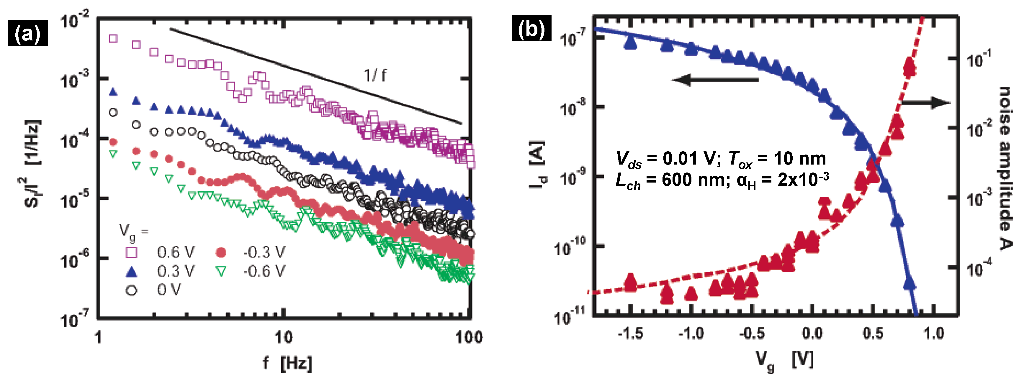
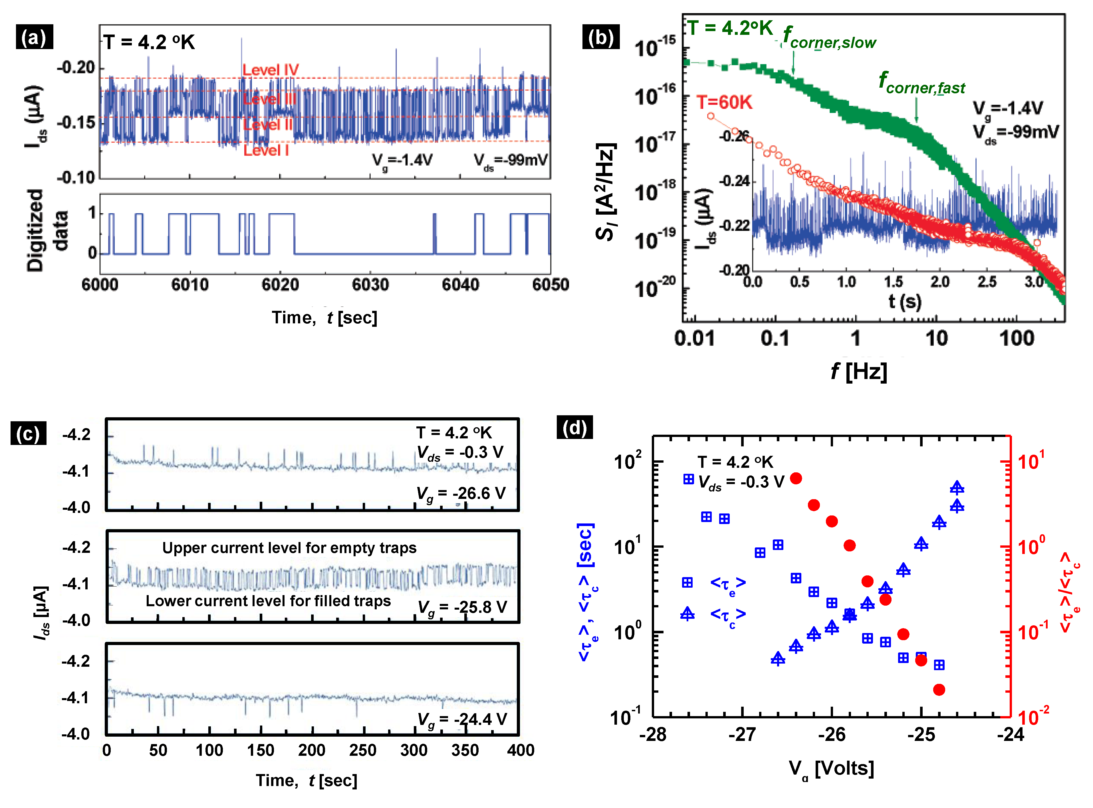
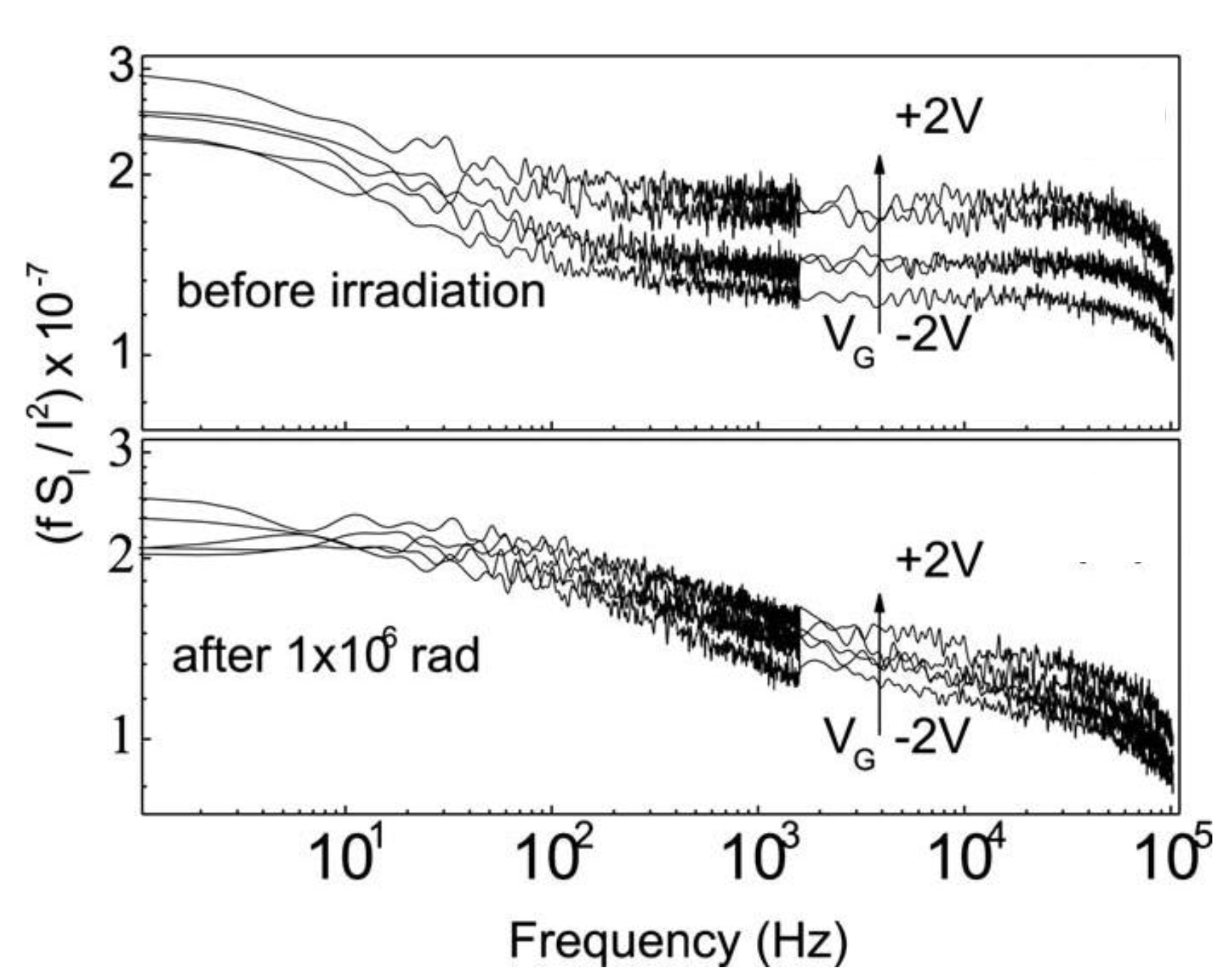
4.4. Low-Frequency Noise in SWCNT-FETs

Low-frequency noise measurement is a general way of characterizing deformations or defects in any nanoscale systems [123,124,125,126,127]. It is also a reliability concern for flash memories [128,129], radio-frequency (RF) circuits [130], and, in general, for many different digital and analog applications employing nanoscale FETs. Among different components of low-frequency noise, the following components are routinely measured: (i) the frequency independent thermal noise component with power spectral density of 4kBTR, which originates from the statistical Brownian motion of carriers at temperature T in a resistive system with resistance R; (ii) the Lorenzian-type noise component with power spectral density ~ 1/[1 + (2πfτ)2], which originates from trapping/detrapping events for a small number of deformations or defects with time constant τ and cut-off frequency fc = 1/τ; and (iii) the flicker noise component with power spectral density ~ 1/f n, which originates from a distribution of trapping/detrapping events.
Table 1. Values of EOT, SWCNT density (D), capacitance ratio (Ξ) [131], maximum electric field with parallel plate assumption (i.e., SWCNT is presumed to form a dense film), and maximum of the average oxide electric field (Eox,max) for reported instances [9,83,94,103,106,107,121,122] of negligible hysteresis in SWCNT-FETs. Here, Ξ = 4π × EOT/εSiO2 × λ0[2/εSiO2 × ln[λ0/d × sinh(2π × EOT/λ0)/π] + CQ−1] [131] (where λ0 = 1000/D is the average distance between each SWCNT, CQ = 4 × 10⁻¹² F/cm is the quantum capacitance [132]), EP,max = VG,max/EOT, and Eox,max = Ξ × EP,max.
ReferenceEOT [nm]D [μm−1]ΞVg,max [V]EP,max [MV cm−1]Eox,max [MV cm−1]Type of Dielectric
[9] Cao et al., Nature ʼ088.2~60.0122.440.02HfO2
[106] Weitz et al., NL ʼ0720.35.480.1620.980.16Octadecyltrichlor osilanated-SiO2
[107] Hur et al., JACS ʼ056.91 (Single CNT)0.0111.450.02Octachlorotrisilox ane-capped organic dielectric
[83] Kim et al., NLʼ035001 (Single CNT)0.36100.20.07SiO2 with PMMA coating
[103] McGill et al., APL ʼ06100~30.3020.20.06Octadecyltrichlor osilanated-SiO2
[121] Hu et al., Phys. E ʼ08200~30.45100.50.23Aminopropyltrieth oxysilaned-SiO2
[131] Kim et al., APL ʼ076.51 (Single CNT)0.0111.540.02Al2O3
[94] Jin et al., AFM ʼ1240~60.2961.50.45Spin-on-glass (SOG) + HfO2
Noise in SWCNT-FETs has been widely studied to understand the origin of deformations or defects in SWCNT lattice and in its surrounding oxides [123,124,125,128,129], and also to explore the effect of radiation damage [133] and chemical exposure [134]. Measured low-frequency noise in SWCNT is much more pronounced than in silicon electronics [135,136] because of the presence of a few carriers for conduction [134]. In addition to structural defects in the SWCNT lattice [135], oxide defects contribute significantly to low-frequency noise behaviors in SWCNT-FETs [137]. (A recent discussion on different sources of low-frequency noise in SWCNT materials and devices can be found in Ref. [138].) Interface defects interact at faster time-scales and hence noise because interface defects are generally overwhelmed by thermal noise at high frequencies. Oxide defects, on the other hand, have comparatively longer and distributed charging and discharging times (either due to distribution in tunneling distance [126,127] or due to distribution in defects’ energetics [139]) that give rise to 1/f behavior in the power spectral density of measured noise in Ids at low frequencies [134,135], as shown in Figure 15a, which is measured for a single s-SWCNT-FET at different Vg [134]. From Hooge’s number fluctuation theory [140] noise power spectral density (SI) can be expressed as,
Electronics 02 00332 i003
where αH is a fitting parameter that varies from device to device. Equation (3) suggests a reduction in noise amplitude A with the increase in carrier number or Ids, as measured for the p-type FET for different Vg (Figure 15b) [134].
Figure 15. (a) Flicker or 1/f noise measured for single s-SWCNT FET at different Vg. (b) Increase in Vg decreases Ids and hence increases noise magnitude following Hooge’s number fluctuation theory [140]. These figures are reprinted with permission from Ref. [134]; © 2006 American Chemical Society.
Electronics 02 00332 g015
Noise measurements in cryogenic conditions reduce thermal noise and also freeze-off some of the defects that contribute to noise at higher temperatures. Responses from the remaining few oxide defects result in random telegraph noise (RTN) with stochastic variation in Ids and discrete current levels [137,141,142,143]. Figure 16a shows RTN obtained from a SWNT-FET (measured at T = 4.2 °K) suggesting four major switching levels resulting from a slow switching defect (whose fluctuation is digitized in the bottom of Figure 16a) and a fast switching defect [142]. Corresponding power density spectrum for these fluctuations is shown in Figure 16b that suggests two overlapping Lorenzian spectrums with corner frequencies (fc) at 0.2 Hz (for the slow defect) and 5.8 Hz (for the fast defect). At higher temperatures (T = 60 °K), however, responses from these two defects are mixed up (inset of Figure 16b) and noise from new defects (with higher fc) shows up. Similar noise analysis at different Vg (Figure 16c) enables one to extract distributions of capture time τc (defined as the time required for a high to low transition in Ids) and emission time τe (defined as the time required for a low to high transition in Ids). These distributions are used to calculate the averages of capture and emission times (<τc> and <τe>) at different Vg (Figure 16d) and, hence, the location of defect causing RTN from the slope of ln(<τe>/<τc>) vs. Vg plot [137].
Figure 16. (a) Random telegraph noise (RTN) measured in a SWCNT-FET at 4.2 °K with Vg = −1.4 V and Vds = −99 mV shows four major switching levels (red dashed lines) due to the presence of one slow (with larger trapping/detrapping time) and one fast (with smaller trapping/detrapping time) defect. The digitized fluctuation for the slow defect is shown in the bottom graph. (b) Noise power spectral density of Figure 16a at 4.2 °K and also for the same device at 60 °K. The inset shows the time domain current data at 60 °K. Spectral density at 4.2 °K shows the cut-off frequencies designating the presence of slow and fast traps. Response from these defects disappears at higher temperatures. (c) Low temperature RTN measurements in another SWCNT-FET at different Vg. (d) Voltage dependence of average capture <τc>, emission <τe> times and their ratios. (a,b) are reprinted with permission from Ref. [142]; © 2008 American Chemical Society and (c,d) are replotted using data from Ref. [137].
Electronics 02 00332 g016
Though RTN analysis has not yet been employed to study the evolution of defects—i.e., reliability in SWCNT-FETs—1/f noise has been used to study the radiation effects in such FETs [133]. An increase in 1/f noise after gamma radiation (Figure 17) suggests generation of defects within the oxide. The next section discusses the radiation effects on SWCNT-FETs in detail.
Figure 17. Measured noise power spectral density at different Vg before and after gamma radiation (reprinted with permission from Ref. [133]; © 2010, AIP Publishing LLC).
Electronics 02 00332 g017

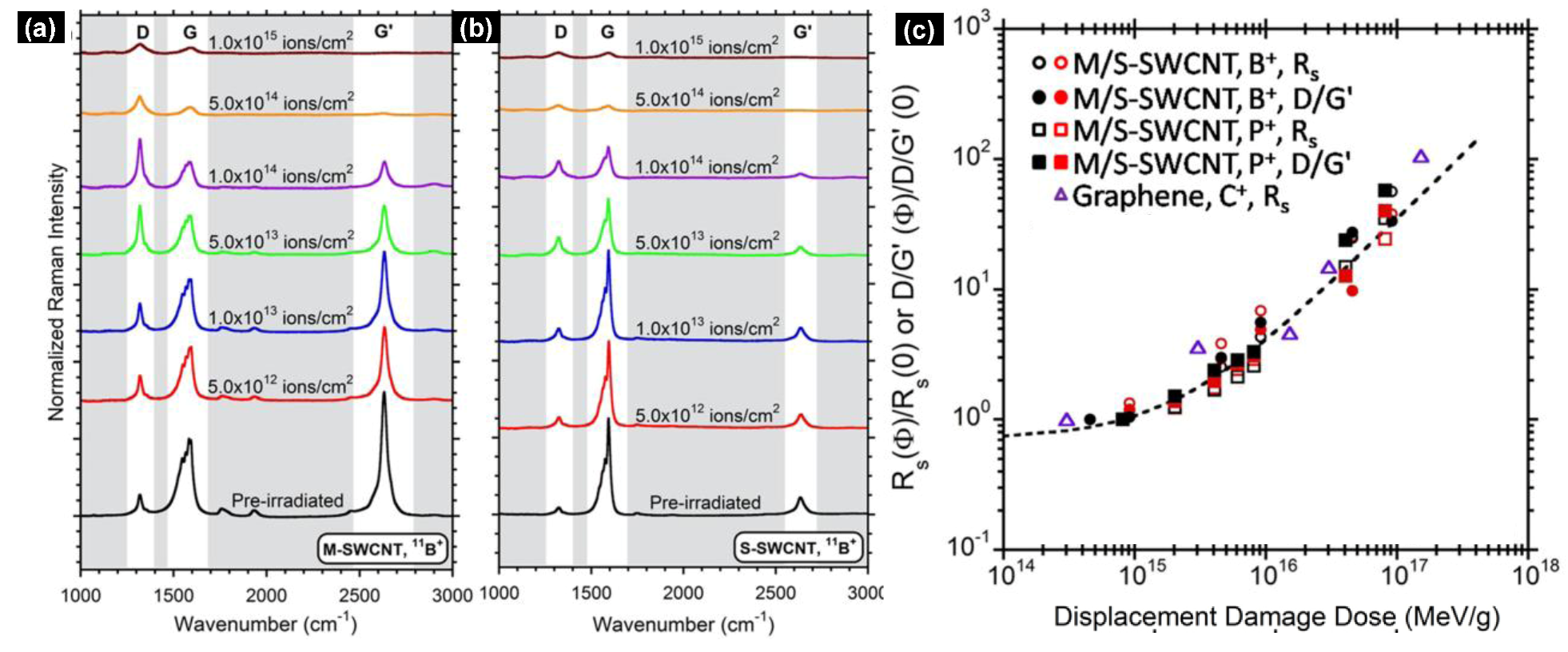
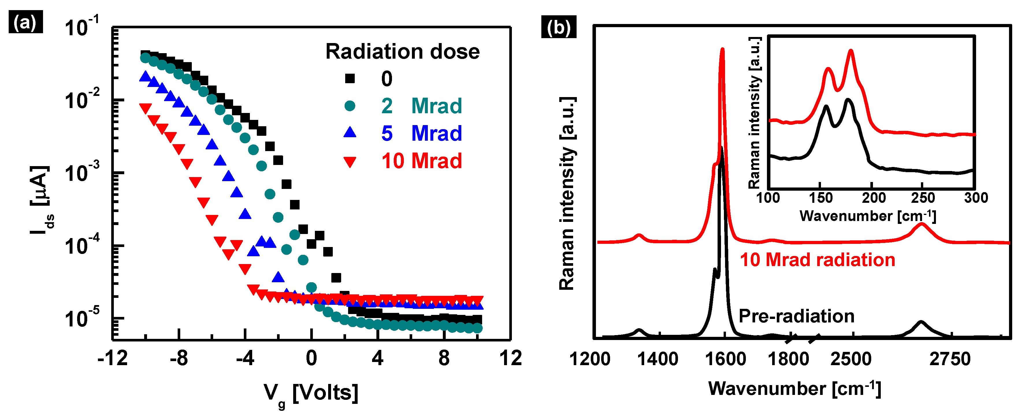
4.5. Radiation Damage in SWCNT-FETs

Promising performance parameters of SWCNTs have initiated studies to explore their potential in terrestrial and space-based applications [133,144,145,146,147,148,149]. In such niche applications, radiation tolerance is one of the key reliability parameters. In this regard, use of SWCNT as a channel showed significant advantages over its silicon-based predecessors. Small cross-sections of SWCNT make it less susceptible to incident radiation particles, unless radiation dose (termed as displacement damage dose, DDD) exceeds ~ 1013 MeV/g [150]. One can evaluate DDD for different types of particles (e.g., alpha, proton, ionized chemical species) by considering the number of particles striking SWCNTs per unit area (i.e., fluence) and the efficiency of these particles in creating defects within the SWCNT lattice (which is quantified using the term non-ionizing energy loss [150]). Damage in SWCNT at high radiation dose (with DDD > 1013 MeV/g) can be monitored using Raman spectroscopy as an increase in intensity at the defect (D)-band wavenumber of ~ 1300 cm−1 [133,146,147,148,151] and also using electrical measurement as an increase in resistance [148,151]. Figure 18a,b show Raman spectra for m- and s-SWCNT-FETs measured at different amount of ionized boron irradiation. Radiation gradually introduces defects within the SWCNT lattice, therefore, increasing the ratio of Raman intensities measured for D- and G+-bands or for D- and G'-bands. (G+- Raman signal comes from the atomic vibration of carbon atoms along the axial direction of SWCNT and peaks at a wavenumber of ~1590 cm−1 with no diameter dependence. On the other hand, G'- Raman signal arises from a two-photon, inter-valley, second-order Raman scattering process and peaks at a wavenumber of ~2700 cm−1 with significant diameter dependence. Both G+ and G' have no influence from structural defects in SWCNTs. (Dresselhaus et. al [152] provide an elaborate review of Raman signal and its origin in different types of SWCNTs.) Ratio of Raman intensities obtained using D- and G'-bands (D/G') are shown to be more sensitive in monitoring the effect of radiation that linearly depends on DDD (Figure 18c), when D/G' at a particular amount of radiation (Φ) is normalized to its value measured before radiation (Φ = 0) [148]. The same linear degradation law also holds for the radiation-induced resistance degradation in SWCNT and graphene.
Figure 18. Raman spectra for (a) m-SWCNT and (b) s-SWCNT thin-films irradiated with 150 keV 11B+ ion. The pre-irradiated spectrum is given as a reference and the intensity of each irradiated sample is normalized to the G band intensity of the reference. (c) Changes in the normalized (with respect to pre-radiated sample) Raman D/G′ ratio and normalized sheet resistance (Rs) with displacement damage dose (DDD) for boron-ion (B+) and phosphorous ion (P+) irradiated m-SWCNTs and s-SWCNTs, and carbon-ion (C+) irradiated graphene (Ref. [153]). The dashed line is a linear fit of all D/G' ratioand Rs values. Figures are reprinted with permission from Ref. [148]; © 2012, AIP Publishing LLC.
Electronics 02 00332 g018
At radiation doses comparable to aerospace environments (i.e., for DDD<1013 MeV/g), only the dielectric layer of SWCNT-FETs are damaged with no damage to the SWCNT lattice [133,146,154]. Radiation in such condition changes Vt of SWCNT-FETs with negligible change in mobility (Figure 19a), therefore, suggests negligible defect formation within the SWCNT. The behavior is also confirmed via Raman spectroscopy (Figure 19b) that shows negligible change in D-band and the radial breathing mode (RBM) Raman signals. (RBM signal comes from the atomic vibration of carbon atoms along the radial of SWCNT and has peaks at wavenumbers in the range of ~100–400 cm−1 with strong diameter dependence [152].) A decrease in Vt with increasing radiation for the p-type SWCNT-FET (Figure 19a) suggests creation of oxide defects that act as hole trapping sites. The situation improves significantly when a comparatively thinner (~23 nm) silicon oxynitride dielectric (grown via plasma-enhanced chemical vapor deposition) replaces the regularly used ~100 nm SiO2 in making SWCNT-FETs for radiation testing [145]. Pre- and post-radiation Ids-Vg measurements (Figure 20) suggest negligible change in FET parameters above threshold (i.e., Vt and μeff). Creation of balanced hole and electron trapping sites within the dielectric [155] and use of thin dielectric that allows the escape of trapped charges [156] are presumed to be the origin of such radiation hardness in these devices. The sub-threshold behavior, on the other hand, shows degradation when the devices are exposed to a negative gate electric field of −1 MV/cm. The origin of such degradation has been attributed to the formation of electron trapping sites within the oxide or at the interface of SWCNT—which requires detailed future analysis. Overall, SWCNT-FETs with thin dielectric offer great potential for space electronics in the future.
Figure 19. (a) Transfer characteristics of an SWCNT-FET measured in vacuum for different doses of Co-60 gamma rays. (b) G-band and G'-band Raman spectra of SWCNTs (98% s-SWCNT enriched thin film) within the FET before (pre-) and after (post-) irradiation in vacuum. Inset shows the Raman spectra in the low wavenumber regime that suggests negligible change in radial breathing modes. These figures are replotted using data from Ref. [146].
Electronics 02 00332 g019
Figure 20. Transfer characteristics of an s-SWCNT FET fabricated with radiation-hard silicon oxynitride gate dielectric. Irradiation is conducted under vacuum with (a) positive, and (b) negative gate electric field of 1 MV/cm. Figures are reprinted with permission from Ref. [145] © Cambridge University Press 2011.
Electronics 02 00332 g020

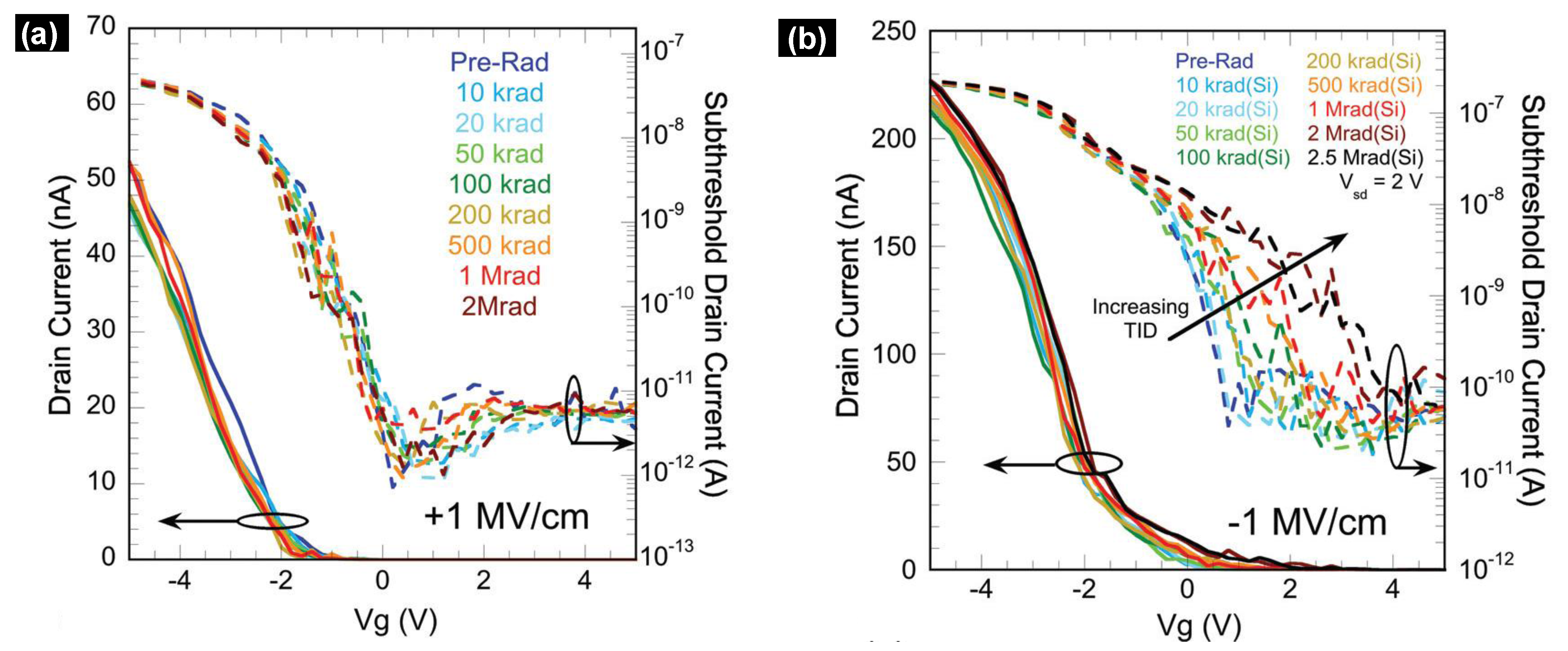
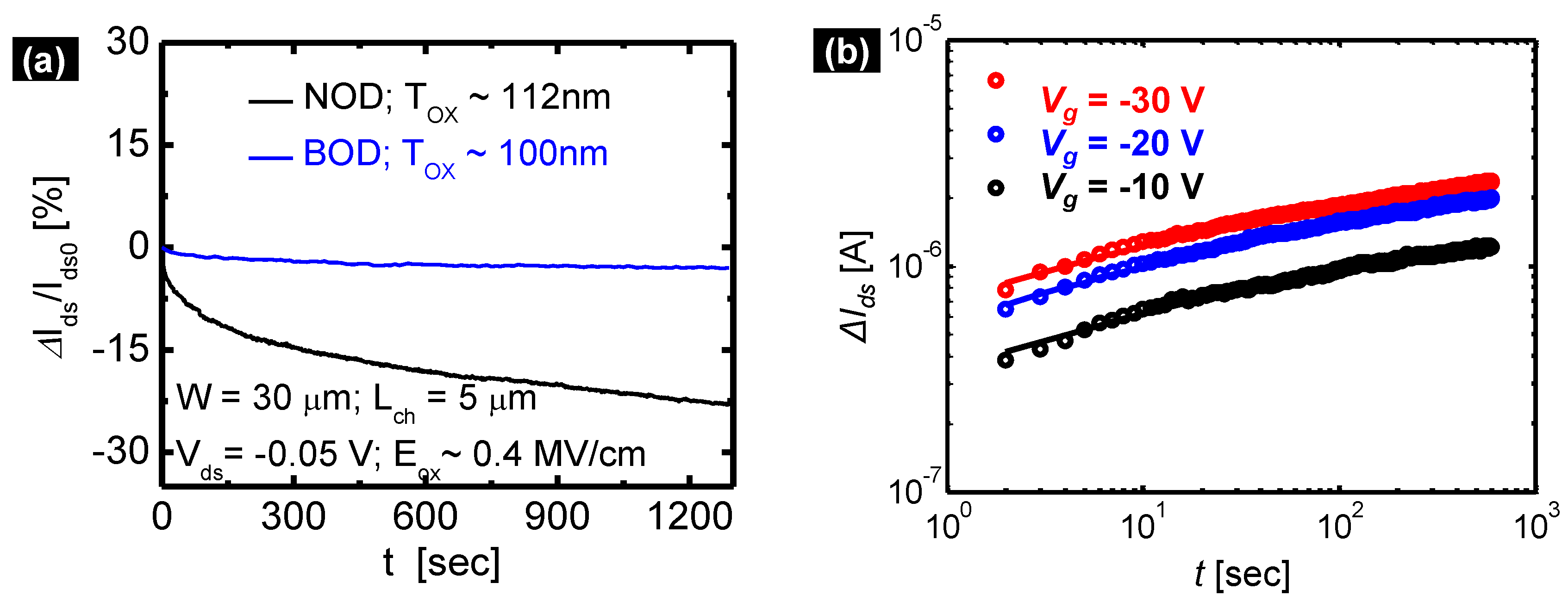
4.6. Performance Degradation in SWCNT-FETs

Performance degradation of transistor parameters over time is a critical reliability concern that dictates the determination of device lifetime. In transistor reliability literature, bias temperature instability [157] and stress-induced leakage current [109] are often used to monitor performance degradation and to probe the dynamics of defects in different regions of the FET. Though hysteresis and low-frequency noise has been widely used to study the nature of defects in SWCNT-FET, detailed analysis of performance degradation over longer time scales is still lacking. Studies of degradation up to a few seconds [95,96] though provides critical information about the nature of some of the defects, projection of performance degradation up to an intended lifetime of 5–10 years requires accelerated tests (at voltages much higher than use condition) and for longer times (1000 s or more), which are widely used in conventional CMOS reliability studies [157].
Some of the recent long-term performance degradation studies in SWCNT-FETs [94] suggest oxide defect as the key contributor for the instability. SWCNT-FETs with a large amount of near-interface oxide defects show significant Ids degradation (ΔIds; Figure 21a) and have a small time constant τ ~ 7 × 10⁴ sec for the fitted stretched exponential forms according to ΔIds = Ids0[1 − exp(−t/τ)β] (where Ids0 is the magnitude of drain current at t = 0, t is the time at which degradation is measured, and τ, β ~ 0.35 are fitting parameters) [158]. On the other hand, devices with a small amount of bulk oxide defects have lower ΔIds and long τ ~ 2 × 10⁷ s (with β ~ 0.35). Moreover, the nature of trapping into oxide defects remains the same at different accelerated stress conditions, as seen from the measured ΔIds at different gate biases (Figure 21b). All these degradation curves can be fitted with a fixed β and a voltage dependent τ (higher for higher Vg) that suggests more and deeper oxide defects are accessible at higher stress biases. Therefore, by using τ as a voltage dependent parameter, one can project reliability of these SWCNT-FETs at different use conditions. Detailed analysis of such degradation by understanding the trapping dynamics (which may require the use of one or multiple time constants [95]) is still lacking.
Figure 21. (a) Percentage change in Ids (ΔIds) relative to its initial value (Ids0) as a function of time (t) for two SWCNT-FETs, one having a large amount of near-interface oxide defects (NOD) and the other having a small amount of bulk oxide defects (BOD). The figure is taken from Ref. [94]; © 2012 WILEY-VCH Verlag GmbH & Co. KGaA, Weinheim. (b) Drain current degradation measured at different gate stress bias Vg. All the degradation curves can be fitted (lines) using a single expression: ΔIds = Ids0[1 − exp(−t/τ)β] with fixed β and voltage dependent τ (higher for higher Vg).
Electronics 02 00332 g021

5. Summary and Outlook

We have discussed different sources of variability and reliability that controls the change in time-zero and time-dependent performance parameters in SWCNT-FETs. Variability in SWCNT FETs performance is mainly attributed to the distributions of SWCNTs’ diameter across the wafer and the presence of hydroxyl-group related interface defects in SWCNTs’ surroundings. The removal of m-SWCNTs and the tightening of diameter distribution for s-SWCNTs via chiral-selective growth [159] or post-processing [50,54], and complete passivation of SWCNTs via removal of hydroxyl groups [83,94] are necessary for controlling variability. Removal of hydroxyl groups from SWCNTs’ surfaces will also be the key to having a reliable SWCNT FET that will operate with reduced performance degradation over its lifetime. In addition, oxide defects keep playing a dominant role in controlling reliability parameters, like low-frequency noise, radiation damage, and long-term performance degradation. Therefore, solutions in terms of having reliable gate dielectrics with less defects [111,160] will not only help current CMOS scaling, but will also assist with the introduction of beyond CMOS devices with SWCNT-based FET.

Acknowledgments

The author acknowledges contributions from John Rogers (University of Illinois) for introducing the presented area of research and also from Sunghun Jin, Frank Du (University of Illinois) for related experiments and discussion. Discussions with Muhammad A. Alam (Purdue University), Cory D. Cress (Naval Research Laboratory), Benji Maruyama (Air Force Research Laboratory), and funding from Air Force Office of Scientific Research (contract number: FA 8650-09-D-5037), Materials Structures and Devices Focus Center (Task ID: 2051.003.4) of Semiconductor Research Corporation are acknowledged for preparation of this review article.

Conflicts of Interest

The authors declare no conflict of interest.

References

  1. Iijima, S. Helical microtubules of graphitic carbon. Nature 1991, 354, 56–58. [Google Scholar] [CrossRef]
  2. Datta, S. Quantum Transport: Atom to Transistor, 2nd ed.; Cambridge University Press: Cambridge CB2 2RU, UK, 2005. [Google Scholar]
  3. Saito, R.; Sato, K.; Oyama, Y.; Jiang, J.; Samsonidze, G.G.; Dresselhaus, G.; Dresselhaus, M.S. Cutting lines near the Fermi energy of single-wall carbon nanotubes. Phys. Rev. B 2005, 72. [Google Scholar] [CrossRef]
  4. Jorio, A.; Pimenta, M.A.; Souza, A.G.; Saito, R.; Dresselhaus, G.; Dresselhaus, M.S. Characterizing carbon nanotube samples with resonance Raman scattering. New J. Phys. 2003, 5. [Google Scholar] [CrossRef]
  5. Zhou, X.J.; Park, J.Y.; Huang, S.M.; Liu, J.; McEuen, P.L. Band structure, phonon scattering, and the performance limit of single-walled carbon nanotube transistors. Phys. Rev. Lett. 2005, 95. [Google Scholar] [CrossRef]
  6. Durkop, T.; Getty, S.A.; Cobas, E.; Fuhrer, M.S. Extraordinary mobility in semiconducting carbon nanotubes. Nano Lett. 2004, 4, 35–39. [Google Scholar] [CrossRef]
  7. Guo, J.; Goasguen, S.; Lundstrom, M.; Datta, S. Metal-insulator-semiconductor electrostatics of carbon nanotubes. Appl. Phys. Lett. 2002, 81, 1486–1488. [Google Scholar] [CrossRef]
  8. Rogers, J.A.; Someya, T.; Huang, Y. Materials and mechanics for stretchable electronics. Science 2010, 327, 1603–1607. [Google Scholar] [CrossRef]
  9. Cao, Q.; Kim, H.S.; Pimparkar, N.; Kulkarni, J.P.; Wang, C.J.; Shim, M.; Roy, K.; Alam, M.A.; Rogers, J.A. Medium-scale carbon nanotube thin-film integrated circuits on flexible plastic substrates. Nature 2008, 454, 495–500. [Google Scholar] [CrossRef]
  10. Sun, Y.; Rogers, J.A. Inorganic semiconductors for flexible electronics. Adv. Mater. 2007, 19, 897–1916. [Google Scholar]
  11. Perelaer, J.; Smith, P.J.; Mager, D.; Soltman, D.; Volkman, S.K.; Subramanian, V.; Korvink, J.G.; Schubert, U.S. Printed electronics: The challenges involved in printing devices, interconnects, and contacts based on inorganic materials. J. Mater.Chem. 2010, 20, 8446–8453. [Google Scholar] [CrossRef]
  12. Cao, Q.; Hur, S.H.; Zhu, Z.T.; Sun, Y.G.; Wang, C.J.; Meitl, M.A.; Shim, M.; Rogers, J.A. Highly bendable, transparent thin-film transistors that use carbon-nanotube-based conductors and semiconductors with elastomeric dielectrics. Adv. Mater. 2006, 18, 304–309. [Google Scholar] [CrossRef]
  13. Xiong, F.; Liao, A.D.; Estrada, D.; Pop, E. Low-power switching of phase-change materials with carbon nanotube electrodes. Science 2011, 332, 568–570. [Google Scholar] [CrossRef]
  14. Kianian, S.; Rosendale, G.; Manning, M.; Hamilton, D.; Huang, X.M.H.; Robinson, K.; Kim, Y.W.; Rueckes, T. A 3D stackable Carbon Nanotube-based nonvolatile memory (NRAM). In Proceedings of the ESSDERC, Sevilla, Spain, 14–16 September, 2010; pp. 404–407.
  15. Rosendale, G.; Kianian, S.; Manning, M.; Hamilton, D.; Huang, X.M.H.; Robinson, K.; Kim, Y.W.; Rueckes, T. A 4 Megabit Carbon Nanotube-based nonvolatile memory (NRAM). In Proceedings of the ESSDERC, Sevilla, Spain, 14–16 September, 2010; pp. 478–481.
  16. Fuhrer, M.S.; Kim, B.M.; Durkop, T.; Brintlinger, T. High-mobility nanotube transistor memory. Nano Lett. 2002, 2, 755–759. [Google Scholar] [CrossRef]
  17. Di Bartolomeo, A.; Yang, Y.; Rinzan, M.B.M.; Boyd, A.K.; Barbara, P. Record endurance for single-walled carbon nanotube-based memory cell. Nanoscale Res. Lett. 2010, 5, 1852–1855. [Google Scholar] [CrossRef]
  18. Jarosz, P.R.; Shaukat, A.; Schauerman, C.M.; Cress, C.D.; Kladitis, P.E.; Ridgley, R.D.; Landi, B.J. High-performance, lightweight coaxial cable from carbon nanotube conductors. ACS Appl. Mater. Interfaces 2012, 4, 1103–1109. [Google Scholar] [CrossRef]
  19. Nair, P.R.; Alam, M.A. Performance limits of nanobiosensors. Appl. Phys. Lett. 2006, 88, 233120:1–233120:3. [Google Scholar]
  20. Pengfei, Q.F.; Vermesh, O.; Grecu, M.; Javey, A.; Wang, O.; Dai, H.J.; Peng, S.; Cho, K.J. Toward large arrays of multiplex functionalized carbon nanotube sensors for highly sensitive and selective molecular detection. Nano Lett. 2003, 3, 347–351. [Google Scholar] [CrossRef]
  21. Collins, P.G.; Bradley, K.; Ishigami, M.; Zettl, A. Extreme oxygen sensitivity of electronic properties of carbon nanotubes. Science 2000, 287, 1801–1804. [Google Scholar] [CrossRef]
  22. Alam, M. Reliability- and process-variation aware design of integrated circuits. Microelectron. Reliab. 2008, 48, 1114–1122. [Google Scholar] [CrossRef]
  23. Lee, Y.H.; McMahon, W.; Mielke, N.; Lu, Y.L.R.; Walstra, S. Managing bias-temperature instability for product reliability. Proc. Int. Symp. VLSI Technol. 2007, 1, 52–53. [Google Scholar]
  24. Moore, G.E. Cramming more components onto integrated circuits (Reprinted from Electronics, pg 114–117, April 19, 1965). Proc. IEEE 1998, 86, 82–85. [Google Scholar] [CrossRef]
  25. Kang, S.J.; Kocabas, C.; Ozel, T.; Shim, M.; Pimparkar, N.; Alam, M.A.; Rotkin, S.V.; Rogers, J.A. High-performance electronics using dense, perfectly aligned arrays of single-walled carbon nanotubes. Nat. Nanotechnol. 2007, 2, 230–236. [Google Scholar] [CrossRef]
  26. Patil, N.; Lin, A.; Myers, E.R.; Ryu, K.; Badmaev, A.; Zhou, C.W.; Wong, H.S.P.; Mitra, S. Wafer-scale growth and transfer of aligned single-walled carbon nanotubes. IEEE Trans. Nanotechnol. 2009, 8, 498–504. [Google Scholar] [CrossRef]
  27. Wang, C.; Badmaev, A.; Jooyaie, A.; Bao, M.Q.; Wang, K.L.; Galatsis, K.; Zhou, C.W. Radio frequency and linearity performance of transistors using high-purity semiconducting carbon nanotubes. ACS Nano 2011, 5, 4169–4176. [Google Scholar] [CrossRef]
  28. Cao, Q.; Han, S.-J.; Tulevski, G.S.; Franklin, A.D.; Haensch, W. Evaluation of field-effect mobility and contact resistance of transistors that use solution-processed single-walled carbon nanotubes. ACS Nano 2012, 6, 6471–6477. [Google Scholar] [CrossRef]
  29. Vijayaraghavan, A.; Blatt, S.; Weissenberger, D.; Oron-Carl, M.; Hennrich, F.; Gerthsen, D.; Hahn, H.; Krupke, R. Ultra-large-scale directed assembly of single-walled carbon nanotube devices. Nano Lett. 2007, 7, 1556–1560. [Google Scholar] [CrossRef]
  30. Bardecker, J.A.; Afzali, A.; Tulevski, G.S.; Graham, T.; Hannon, J.B.; Jen, A.K.Y. Directed assembly of single-walled carbon nanotubes via drop-casting onto a UV-patterned photosensitive monolayer. J. Am. Chem. Soc. 2008, 130, 7226–7227. [Google Scholar] [CrossRef]
  31. Park, H.; Afzali, A.; Han, S.-J.; Tulevski, G.S.; Franklin, A.D.; Tersoff, J.; Hannon, J.B.; Haensch, W. High-density integration of carbon nanotubes via chemical self-assembly. Nat. Nanotechnol. 2012, 7, 787–791. [Google Scholar] [CrossRef]
  32. Cao, J.; Nyffeler, C.; Lister, K.; Ionescu, A.M. Resist-assisted assembly of single-walled carbon nanotube devices with nanoscale precision. Carbon 2012, 50, 1720–1726. [Google Scholar] [CrossRef]
  33. Wang, J. Carbon-nanotube based electrochemical biosensors: A review. Electroanalysis 2005, 17, 7–14. [Google Scholar] [CrossRef]
  34. Javey, A.; Guo, J.; Farmer, D.B.; Wang, Q.; Wang, D.W.; Gordon, R.G.; Lundstrom, M.; Dai, H.J. Carbon nanotube field-effect transistors with integrated ohmic contacts and high-k gate dielectrics. Nano Lett. 2004, 4, 447–450. [Google Scholar] [CrossRef]
  35. Cao, Q.; Han, S.-J.; Tulevski, G.S.; Zhu, Y.; Lu, D.D.; Haensch, W. Arrays of single-walled carbon nanotubes with full surface coverage for high-performance electronics. Nat. Nanotechnol. 2013, 8, 180–186. [Google Scholar] [CrossRef]
  36. Franklin, A.D.; Wong, H.S.P.; Lin, A.; Chen, Z.H. Current scaling in aligned carbon nanotube array transistors with local bottom gating. IEEE Electron Device Lett. 2010, 31, 644–646. [Google Scholar] [CrossRef]
  37. Cao, J.; Ionescu, A.M. Self-aligned lateral dual-gate suspended-body single-walled carbon nanotube field-effect transistors. Appl. Phys. Lett. 2012, 100, 063103:1–063103:3. [Google Scholar]
  38. Franklin, A.D.; Koswatta, S.O.; Farmer, D.B.; Smith, J.T.; Gignac, L.; Breslin, C.M.; Han, S.-J.; Tulevski, G.S.; Miyazoe, H.; Haensch, W.; et al. Carbon nanotube complementary wrap-gate transistors. Nano Lett. 2013, 13, 2490–2495. [Google Scholar] [CrossRef]
  39. Pimparkar, N.; Alam, M.A. A “bottom-up” redefinition for mobility and the effect of poor tube-tube contact on the performance of CNT nanonet thin-film transistors. IEEE Electron Device Lett. 2008, 29, 1037–1039. [Google Scholar] [CrossRef]
  40. Pimparkar, N.; Guo, J.; Alam, M.A. Performance assessment of subpercolating nanobundle network thin-film transistors by an analytical model. IEEE Trans. Electron Devices 2007, 54, 637–644. [Google Scholar] [CrossRef]
  41. Raychowdhury, A.; de, V.K.; Kurtin, J.; Borkar, S.Y.; Roy, K.; Keshavarzi, A. Variation tolerance in a multichannel carbon-nanotube transistor for high-speed digital circuits. IEEE Trans. Electron Devices 2009, 56, 383–392. [Google Scholar] [CrossRef]
  42. Nessim, G.D. Properties, synthesis, and growth mechanisms of carbon nanotubes with special focus on thermal chemical vapor deposition. Nanoscale 2010, 2, 1306–1323. [Google Scholar] [CrossRef]
  43. Cao, Q.; Rogers, J.A. Ultrathin films of single-walled carbon nanotubes for electronics and sensors: A review of fundamental and applied aspects. Adv. Mater. 2009, 21, 29–53. [Google Scholar] [CrossRef]
  44. Islam, A.E.; Du, F.; Ho, X.; Jin, S.H.; Dunham, S.; Rogers, J.A. Effect of variations in diameter and density on the statistics of aligned array carbon-nanotube field effect transistors. J. Appl. Phys. 2012, 111, 054511:1–054511:7. [Google Scholar]
  45. Salamat, S.; Ho, X.N.; Rogers, J.A.; Alam, M.A. Intrinsic performance variability in aligned array CNFETs. IEEE Trans. Nanotechnol. 2011, 10, 439–444. [Google Scholar] [CrossRef]
  46. Sarker, B.K.; Shekhar, S.; Khondaker, S.I. Semiconducting enriched carbon nanotube aligned arrays of tunable density and their electrical transport properties. ACS Nano 2011, 5, 6297–6305. [Google Scholar] [CrossRef]
  47. Kocabas, C.; Kim, H.-S.; Banks, T.; Rogers, J.A.; Pesetski, A.A.; Baumgardner, J.E.; Krishnaswamy, S.V.; Zhang, H. Radio frequency analog electronics based on carbon nanotube transistors. Proc. Natl. Acad. Sci. USA 2008, 105, 1405–1409. [Google Scholar] [CrossRef]
  48. Hong, S.W.; Banks, T.; Rogers, J.A. Improved density in aligned arrays of single-walled carbon nanotubes by sequential chemical vapor deposition on quartz. Adv. Mater. 2010, 22, 1826–1830. [Google Scholar] [CrossRef]
  49. Xiao, J.L.; Dunham, S.; Liu, P.; Zhang, Y.W.; Kocabas, C.; Moh, L.; Huang, Y.G.; Hwang, K.C.; Lu, C.; Huang, W.; et al. Alignment controlled growth of single-walled carbon nanotubes on quartz substrates. Nano Lett. 2009, 9, 4311–4319. [Google Scholar] [CrossRef]
  50. Arnold, M.S.; Green, A.A.; Hulvat, J.F.; Stupp, S.I.; Hersam, M.C. Sorting carbon nanotubes by electronic structure using density differentiation. Nat. Nanotechnol. 2006, 1, 60–65. [Google Scholar] [CrossRef]
  51. Heller, D.A.; Mayrhofer, R.M.; Baik, S.; Grinkova, Y.V.; Usrey, M.L.; Strano, M.S. Concomitant length and diameter separation of single-walled carbon nanotubes. J. Am. Chem. Soc. 2004, 126, 14567–14573. [Google Scholar] [CrossRef]
  52. Zheng, M.; Jagota, A.; Strano, M.S.; Santos, A.P.; Barone, P.; Chou, S.G.; Diner, B.A.; Dresselhaus, M.S.; McLean, R.S.; Onoa, G.B.; et al. Structure-based carbon nanotube sorting by sequence-dependent DNA assembly. Science 2003, 302, 1545–1548. [Google Scholar] [CrossRef]
  53. Stokes, P.; Khondaker, S.I. High quality solution processed carbon nanotube transistors assembled by dielectrophoresis. Appl. Phys. Lett. 2010, 96, 083110:1–083110:3. [Google Scholar]
  54. Jin, S.H.; Dunham, S.N.; Song, J.; Xie, X.; Kim, J.-H.; Lu, C.; Islam, A.; Du, F.; Kim, J.; Felts, J.; et al. Using nanoscale thermocapillary flows to create arrays of purely semiconducting single-walled carbon nanotubes. Nat. Nanotechnol. 2013, 8, 347–355. [Google Scholar] [CrossRef]
  55. Shulaker, M.M.; Wei, H.; Patil, N.; Provine, J.; Chen, H.Y.; Wong, H.S.P.; Mitra, S. Linear increases in carbon nanotube density through multiple transfer technique. Nano Lett. 2011, 11, 1881–1886. [Google Scholar] [CrossRef]
  56. Wang, C.; Ryu, K.; de Arco, L.G.; Badmaev, A.; Zhang, J.; Lin, X.; Che, Y.; Zhou, C. Synthesis and device applications of high-density aligned carbon nanotubes using low-pressure chemical vapor deposition and stacked multiple transfer. Nano Res. 2010, 3, 831–842. [Google Scholar] [CrossRef]
  57. Kim, W.; Javey, A.; Tu, R.; Cao, J.; Wang, Q.; Dai, H.J. Electrical contacts to carbon nanotubes down to 1 nm in diameter. Appl. Phys. Lett. 2005, 87, 173101:1–173101:3. [Google Scholar]
  58. Tseng, Y.C.; Phoa, K.; Carlton, D.; Bokor, J. Effect of diameter variation in a large set of carbon nanotube transistors. Nano Lett. 2006, 6, 1364–1368. [Google Scholar] [CrossRef]
  59. Chen, Z.H.; Appenzeller, J.; Knoch, J.; Lin, Y.M.; Avouris, P. The role of metal-nanotube contact in the performance of carbon nanotube field-effect transistors. Nano Lett. 2005, 5, 1497–1502. [Google Scholar] [CrossRef]
  60. Nosho, Y.; Ohno, Y.; Kishimoto, S.; Mizutani, T. n-Type carbon nanotube field-effect transistors fabricated by using Ca contact electrodes. Appl. Phys. Lett. 2005, 86, 073105:1–073105:3. [Google Scholar]
  61. Wang, S.; Zeng, Q.S.; Yang, L.J.; Zhang, Z.Y.; Wang, Z.X.; Pei, T.A.; Ding, L.; Liang, X.L.; Gao, M.; Li, Y.; et al. High-performance carbon nanotube light-emitting diodes with Asymmetric contacts. Nano Lett. 2011, 11, 23–29. [Google Scholar] [CrossRef]
  62. Wei, H.; Chen, H.-Y.; Liyanage, L.; Wong, H.S.P.; Mitra, S. Air-Stable Technique for Fabricating n-Type Carbon Nanotube FETs. In Proceedings of the IEEE International Electron Devices Meeting, Washington DC, USA, 5–7 December, 2011; pp. 505–508.
  63. Franklin, A.D.; Chen, Z.H. Length scaling of carbon nanotube transistors. Nat. Nanotechnol. 2010, 5, 858–862. [Google Scholar] [CrossRef]
  64. Franklin, A.D.; Luisier, M.; Han, S.-J.; Tulevski, G.; Breslin, C.M.; Gignac, L.; Lundstrom, M.S.; Haensch, W. Sub-10 nm carbon nanotube transistor. Nano Lett. 2012, 12, 758–762. [Google Scholar] [CrossRef]
  65. Lin, Y.M.; Appenzeller, J.; Avouris, P. Novel Carbon Nanotube FET Design with Tunable Polarity. In Proceedings of the IEEE International Electron Devices Meeting, SanFrancisco, CA, 13–15 December, 2004; pp. 687–690.
  66. Sze, S.M. Physics of Semiconductor Devices, 2nd ed.; John Wiley & Sons: Hoboken, NY, USA, 1981. [Google Scholar]
  67. Ho, X.; Ye, L.; Rotkin, S.V.; Cao, Q.; Unarunotai, S.; Salamat, S.; Alam, M.A.; Rogers, J.A. Scaling properties in transistors that use aligned arrays of single-walled carbon nanotubes. Nano Lett. 2010, 10, 499–503. [Google Scholar] [CrossRef]
  68. Deshpande, V.V.; Chandra, B.; Caldwell, R.; Novikov, D.S.; Hone, J.; Bockrath, M. Mott insulating state in ultraclean carbon nanotubes. Science 2009, 323, 106–110. [Google Scholar] [CrossRef]
  69. Charlier, J.C.; Blase, X.; Roche, S. Electronic and transport properties of nanotubes. Rev. Mod. Phys. 2007, 79, 677–732. [Google Scholar] [CrossRef]
  70. Wahab, M.A.; Jin, S.H.; Islam, A.E.; Kim, J.; Kim, J.-H.; Yeo, W.-H.; Lee, D.J.; Chung, H.U.; Rogers, J.A.; Alam, M.A. Electrostatic dimension of aligned-array carbon nanotube field-effect transistors. ACS Nano 2013, 7, 1299–1308. [Google Scholar] [CrossRef]
  71. Rutherglen, C.; Jain, D.; Burke, P. Nanotube electronics for radiofrequency applications. Nat. Nanotechnol. 2009, 4, 811–819. [Google Scholar] [CrossRef]
  72. Ryu, K.; Badmaev, A.; Wang, C.; Lin, A.; Patil, N.; Gomez, L.; Kumar, A.; Mitra, S.; Wong, H.S.P.; Zhou, C.W. CMOS-analogous wafer-scale nanotube-on-insulator approach for submicrometer devices and integrated circuits using aligned nanotubes. Nano Lett. 2009, 9, 189–197. [Google Scholar] [CrossRef]
  73. Ishikawa, F.N.; Chang, H.K.; Ryu, K.; Chen, P.C.; Badmaev, A.; de Arco, L.G.; Shen, G.Z.; Zhou, C.W. Transparent electronics based on transfer printed aligned carbon nanotubes on rigid and flexible substrates. ACS Nano 2009, 3, 73–79. [Google Scholar] [CrossRef]
  74. Feng, C.; Liu, K.; Wu, J.S.; Liu, L.; Cheng, J.S.; Zhang, Y.Y.; Sun, Y.H.; Li, Q.Q.; Fan, S.S.; Jiang, K.L. Flexible, stretchable, transparent conducting films made from superaligned carbon nanotubes. Adv. Funct. Mater. 2010, 20, 885–891. [Google Scholar] [CrossRef]
  75. Ago, H.; Imamoto, K.; Ishigami, N.; Ohdo, R.; Ikeda, K.-I.; Tsuji, M. Competition and cooperation between lattice-oriented growth and step-templated growth of aligned carbon nanotubes on sapphire. Appl. Phys. Lett. 2007, 90, 123112:1–123112:3. [Google Scholar]
  76. Ismach, A.; Segev, L.; Wachtel, E.; Joselevich, E. Atomic-step-templated formation of single wall carbon nanotube patterns. Angew. Chem. Int. Ed. 2004, 43, 6140–6143. [Google Scholar] [CrossRef]
  77. Kocabas, C.; Kang, S.J.; Ozel, T.; Shim, M.; Rogers, J.A. Improved synthesis of aligned arrays of single-walled carbon nanotubes and their implementation in thin film type transistors. J. Phys. Chem. C 2007, 111, 17879–17886. [Google Scholar] [CrossRef]
  78. Huang, H.J.; Maruyama, R.; Noda, K.; Kajiura, H.; Kadono, K. Preferential destruction of metallic single-walled carbon nanotubes by laser irradiation. J. Phys. Chem. B 2006, 110, 7316–7320. [Google Scholar]
  79. Collins, P.C.; Arnold, M.S.; Avouris, P. Engineering carbon nanotubes and nanotube circuits using electrical breakdown. Science 2001, 292, 706–709. [Google Scholar] [CrossRef]
  80. Chen, C.X.; Yan, L.J.; Kong, E.S.W.; Zhang, Y.F. Ultrasonic nanowelding of carbon nanotubes to metal electrodes. Nanotechnology 2006, 17, 2192–2197. [Google Scholar] [CrossRef]
  81. Perebeinos, V.; Avouris, P. Impact excitation by hot carriers in carbon nanotubes. Phy. Rev. B 2006, 74. [Google Scholar] [CrossRef]
  82. Liao, A.; Zhao, Y.; Pop, E. Avalanche-induced current enhancement in semiconducting carbon nanotubes. Phys. Rev. Lett. 2008, 101, 256804. [Google Scholar] [CrossRef]
  83. Kim, W.; Javey, A.; Vermesh, O.; Wang, O.; Li, Y.M.; Dai, H.J. Hysteresis caused by water molecules in carbon nanotube field-effect transistors. Nano Lett. 2003, 3, 193–198. [Google Scholar] [CrossRef]
  84. Polishchuk, I.; Ranade, P.; King, T.J.; Hu, C.M. Dual work function metal gate CMOS technology using metal interdiffusion. IEEE Electron Device Lett. 2001, 22, 444–446. [Google Scholar] [CrossRef]
  85. Lim, A.E.J.; Hwang, W.S.; Wang, X.P.; Lai, D.M.Y.; Samudra, G.S.; Kwong, D.L.; Yeo, Y.C. Metal-gate work function modulation using hafnium alloys obtained by the interdiffusion of thin metallic layers. J. Electrochem. Soc. 2007, 154, H309–H313. [Google Scholar] [CrossRef]
  86. Franklin, A.D.; Tulevski, G.S.; Han, S.-J.; Shahrjerdi, D.; Cao, Q.; Chen, H.-Y.; Wong, H.S.P.; Haensch, W. Variability in carbon nanotube transistors: Improving device-to-device consistency. ACS Nano 2012, 6, 1109–1115. [Google Scholar] [CrossRef]
  87. Paul, B.C.; Fujita, S.; Okajima, M.; Lee, T.H.; Wong, H.S.P.; Nishi, Y. Impact of a process variation on nanowire and nanotube device performance. IEEE Trans. Electron Devices 2007, 54, 2369–2376. [Google Scholar] [CrossRef]
  88. Wong, H.S.P.; Mitra, S.; Akinwande, D.; Beasley, C.; Chai, Y.; Chen, H.-Y.; Chen, X.; Close, G.; Deng, J.; Hazeghi, A.; et al. Carbon Nanotube Electronics—Materials, Devices, Circuits, Design, Modeling, and Performance Projection. In Proceedings of the IEEE International Electron Devices Meeting, Washington DC, USA, 5–7 December, 2011; pp. 501–504.
  89. Balijepalli, A.; Sinha, S.; Cao, Y. Compact Modeling of Carbon Nanotube Transistor for Early Stage Process-Design Exploration. In Proceedings of the 2007 ACM/IEEE International Symposium on Low Power Electronics and Design (ISLPED), Portland, OR, USA, 27–29 August 2007.
  90. Zhang, G.; Qi, P.; Wang, X.; Lu, Y.; Li, X.; Tu, R.; Bangsaruntip, S.; Mann, D.; Zhang, L.; Dai, H. Selective etching of metallic carbon nanotubes by gas-phase reaction. Science 2006, 314, 974–977. [Google Scholar] [CrossRef]
  91. Zhang, J.; Patil, N.P.; Hazeghi, A.; Wong, H.S.P.; Mitra, S. Characterization and design of Logic circuits in the presence of carbon nanotube density variations. IEEE Trans. Comput. Aided Des. Integr. Circuits Syst. 2011, 30, 1103–1113. [Google Scholar] [CrossRef]
  92. Boslaugh, S.; Watters, P.A. Safari Tech Books Online. In Statistics in a Nutshell; OʼReilly Media: Sebastopol, CA, USA, 2008. [Google Scholar]
  93. Sun, Y.; Tuleski, G.; Han, S.-J.; Haensch, W.; Chen, Z. Improve Variability in Carbon Nanotube FETs by Scaling. In Proceedings of the Device Research Conference, NotreDame, IN, USA, 21–23 June, 2010; pp. 283–284.
  94. Jin, S.H.; Islam, A.E.; Kim, T.-I.; Kim, J.-H.; Alam, M.A.; Rogers, J.A. Sources of hysteresis in carbon nanotube field-effect transistors and their elimination via methylsiloxane encapsulants and optimized growth. Adv. Funct. Mater. 2012, 22, 2276–2284. [Google Scholar] [CrossRef]
  95. Qu, M.; Qiu, Z.-J.; Zhang, Z.-B.; Li, H.; Li, J.; Zhang, S.-L. Charge-injection-induced time decay in carbon nanotube network-based FETs. IEEE Electron Device Lett. 2010, 31, 1098–1100. [Google Scholar] [CrossRef]
  96. Peng, N.; Zhang, Q.; Yuan, S.; Li, H.; Tian, J.; Chan, L. Current instability of carbon nanotube field effect transistors. Nanotechnology 2007, 18. [Google Scholar] [CrossRef]
  97. Ellison, M.D.; Crotty, M.J.; Koh, D.; Spray, R.L.; Tate, K.E. Adsorption of NH3 and NO2 on single-walled carbon nanotubes. J. Phys. Chem. B 2004, 108, 7938–7943. [Google Scholar] [CrossRef]
  98. Yao, Z.; Postma, H.W.C.; Balents, L.; Dekker, C. Carbon nanotube intramolecular junctions. Nature 1999, 402, 273–276. [Google Scholar] [CrossRef]
  99. Robinson, J.A.; Snow, E.S.; Badescu, S.C.; Reinecke, T.L.; Perkins, F.K. Role of defects in single-walled carbon nanotube chemical sensors. Nano Lett. 2006, 6, 1747–1751. [Google Scholar] [CrossRef]
  100. Zhou, C.W.; Kong, J.; Yenilmez, E.; Dai, H.J. Modulated chemical doping of individual carbon nanotubes. Science 2000, 290, 1552–1555. [Google Scholar] [CrossRef]
  101. Zhuravlev, L.T. The surface chemistry of amorphous silica. Zhuravlev model. Colloids Surfaces Physicochem. Eng. Asp. 2000, 173, 1–38. [Google Scholar] [CrossRef]
  102. Chakrapani, V.; Anderson, A.B.; Wolter, S.D.; Stoner, B.R.; Sumanasekera, G.U.; Angus, J.C. Charge transfer equilibria between diamond and an aqueous oxygen electrochemical redox couple. Science 2007, 318, 1424–1430. [Google Scholar] [CrossRef]
  103. McGill, S.A.; Rao, S.G.; Manandhar, P.; Xiong, P.; Hong, S. High-performance, hysteresis-free carbon nanotube field-effect transistors via directed assembly. Appl. Phys. Lett. 2006, 89, 163123:1–163123:3. [Google Scholar]
  104. Aguirre, C.M.; Levesque, P.L.; Paillet, M.; Lapointe, F.; St-Antoine, B.C.; Desjardins, P.; Martel, R. The role of the oxygen/water redox couple in suppressing electron conduction in field-effect transistors. Adv. Mater. 2009, 21. [Google Scholar] [CrossRef]
  105. Levesque, P.L.; Sabri, S.S.; Aguirre, C.M.; Guillemette, J.; Siaj, M.; Desjardins, P.; Szkopek, T.; Martel, R. Probing charge transfer at surfaces using graphene transistors. Nano Lett. 2011, 11, 132–137. [Google Scholar] [CrossRef]
  106. Weitz, R.T.; Zschieschang, U.; Effenberger, F.; Klauk, H.; Burghard, M.; Kern, K. High-performance carbon nanotube field effect transistors with a thin gate dielectric based on a self-assembled monolayer. Nano Lett. 2007, 7, 22–27. [Google Scholar] [CrossRef]
  107. Hur, S.H.; Yoon, M.H.; Gaur, A.; Shim, M.; Facchetti, A.; Marks, T.J.; Rogers, J.A. Organic nanodielectrics for low voltage carbon nanotube thin film transistors and complementary logic gates. J. Am. Chem. Soc. 2005, 127, 13808–13809. [Google Scholar]
  108. Reisman, A.; Williams, C.K.; Maldonado, J.R. Generation and annealing of defects in silicon dioxide. J. Appl. Phys. 1987, 62, 868–874. [Google Scholar] [CrossRef]
  109. Alam, M.A. SILC as a measure of trap generation and predictor of T-BD in ultrathin oxides. IEEE Trans. Electron Devices 2002, 49, 226–231. [Google Scholar] [CrossRef]
  110. Solomon, P. Breakdown in silicon-oxide. J. Vac. Sci. Technol. 1977, 14, 1122–1130. [Google Scholar] [CrossRef]
  111. Ribes, G.; Mitard, J.; Denais, M.; Bruyere, S.; Monsieur, F.; Parthasarathy, C.R.; Vincent, E.; Ghibaudo, G. Review on high-k dielectrics reliability issues. IEEE Trans. Device Mater Reliab. 2005, 5, 5–19. [Google Scholar] [CrossRef]
  112. Lenahan, P.M.; Dressendorfer, P.V. Hole traps and trivalent silicon centers in metal-oxide silicon devices. J. Appl. Phys. 1984, 55, 3495–3499. [Google Scholar] [CrossRef]
  113. Lenahan, P.M. Dominating defects in the MOS system: Pb and E' centers. In Defects in Microelectronic Materials and Devices; Fleetwood, S.P.D., Schrimpf, R.D., Eds.; CRC Press: Taylor and Francis Group, Boca Raton, FL, USA, 2009; pp. 163–214. [Google Scholar]
  114. Skuja, L. Optically active oxygen-deficiency-related centers in amorphous silicon dioxide. J. Non Cryst. Solids 1998, 239, 16–48. [Google Scholar] [CrossRef]
  115. Spinelli, A.S.; Lacaita, A.L.; Rigamonti, M.; Ielmini, D.; Ghidini, G. Separation of electron and hole traps by transient current analysis. Microelectron. Eng. 1999, 48, 151–154. [Google Scholar] [CrossRef]
  116. Hongo, H.; Nihey, F.; Yorozu, S. Relationship between carbon nanotube density and hysteresis characteristics of carbon nanotube random network-channel field effect transistors. J. Appl. Phys. 2010, 107, 094501:1–094501:9. [Google Scholar]
  117. Di Bartolomeo, A.; Rinzan, M.; Boyd, A.K.; Yang, Y.; Guadagno, L.; Giubileo, F.; Barbara, P. Electrical properties and memory effects of field-effect transistors from networks of single- and double-walled carbon nanotubes. Nanotechnology 2010, 21. [Google Scholar] [CrossRef]
  118. Memming, R. Semiconductor Electrochemistry; Wiley-VCH: Weinheim, NY, USA, 2001. [Google Scholar]
  119. Shockley, W.; Read, W.T. Statistics of the recombinations of holes and electrons. Phys. Rev. 1952, 87, 835–842. [Google Scholar] [CrossRef]
  120. Chang, M.H.; Zhang, J.F.; Zhang, W.D. Assessment of capture cross sections and effective density of electron traps generated in silicon dioxides. IEEE Trans. Electron Devices 2006, 53, 1347–1354. [Google Scholar] [CrossRef]
  121. Hu, P.; Zhang, C.; Fasoli, A.; Scardaci, V.; Pisana, S.; Hasan, T.; Robertson, J.; Milne, W.I.; Ferrari, A.C. Hysteresis suppression in self-assembled single-wall nanotube field effect transistors. Phys. ELowDimens. Syst. Nanostruct. 2008, 40, 2278–2282. [Google Scholar] [CrossRef]
  122. Kim, S.K.; Xuan, Y.; Ye, P.D.; Mohammadi, S.; Back, J.H.; Shim, M. Atomic layer deposited Al2O3 for gate dielectric and passivation layer of single-walled carbon nanotube transistors. Appl. Phys. Lett. 2007, 90, 163108:1–163108:3. [Google Scholar]
  123. Kirton, M.J.; Uren, M.J. Noise in solid-state microstructures—A new perspective on individual defects, interface states and low-frequency (1/f) noise. Adv. Phys. 1989, 38, 367–468. [Google Scholar] [CrossRef]
  124. Vandamme, L.K.J. Noise as a diagnostic tool for quality and reliability of electronic devices. IEEE Trans. Electron Devices 1994, 41, 2176–2187. [Google Scholar] [CrossRef]
  125. Vandamme, L.K.J.; Li, X.S.; Rigaud, D. 1/f Noise in MOS Devices, Mobility or Number Fluctuations. IEEE Trans. Electron Devices 1994, 41, 1936–1945. [Google Scholar] [CrossRef]
  126. Weissman, M.B. 1/f noise and other slow, nonexponential kinetics in condensed matter. Rev. Mod. Phys. 1988, 60, 537–571. [Google Scholar] [CrossRef]
  127. Weissman, M.B. Low-frequency noise as a tool to study disordered materials. Annu. Rev. Mater. Sci. 1996, 26, 395–429. [Google Scholar] [CrossRef]
  128. Kurata, H.; Otsuga, K.; Kotabe, A.; Kajiyama, S.; Osabe, T.; Sasago, Y.; Narumi, S.; Tokami, K.; Kamohara, S.; Tsuchiya, O. Random telegraph signal in flash memory: Its impact on scaling of multilevel flash memory beyond the 90-nm node. IEEE J. SolidState Circuits 2007, 42, 1362–1369. [Google Scholar] [CrossRef]
  129. Ghetti, A.; Compagnoni, C.M.; Biancardi, F.; Lacaita, A.L.; Beltrami, S.; Chiavarone, L.; Spinelli, A.S.; Visconti, A. Scaling trends for random telegraph noise in deca-nanometer Flash memories. In Proceedings of the IEEE International Electron Devices Meeting Technical Digest, SanFrancisco, CA, 15–17 December, 2008; pp. 835–838.
  130. Gierkink, S.L.J.; Klumperink, E.A.M.; van der Wel, A.P.; Hoogzaad, G.; van Tuijl, E.; Nauta, B. Intrinsic 1/f device noise reduction and its effect on phase noise in CMOS ring oscillators. IEEE J. SolidState Circuits 1999, 34, 1022–1025. [Google Scholar] [CrossRef]
  131. Cao, Q.; Xia, M.G.; Kocabas, C.; Shim, M.; Rotkin, S.V.; Rogers, J.A. Gate capacitance coupling of singled-walled carbon nanotube thin-film transistors. Appl. Phys. Lett. 2007, 90, 023516:1–023516:3. [Google Scholar]
  132. Rosenblatt, S.; Yaish, Y.; Park, J.; Gore, J.; Sazonova, V.; McEuen, P.L. High performance electrolyte gated carbon nanotube transistors. Nano Lett. 2002, 2, 869–872. [Google Scholar] [CrossRef]
  133. Vitusevich, S.A.; Sydoruk, V.A.; Petrychuk, M.V.; Danilchenko, B.A.; Klein, N.; Offenhaeusser, A.; Ural, A.; Bosman, G. Transport properties of single-walled carbon nanotube transistors after gamma radiation treatment. J. Appl. Phys. 2010, 107, 063701:1–063701:6. [Google Scholar]
  134. Lin, Y.-M.; Appenzeller, J.; Knoch, J.; Chen, Z.; Avouris, P. Low-frequency current fluctuations in individual semiconducting single-wall carbon nanotubes. Nano Lett. 2006, 6, 930–936. [Google Scholar] [CrossRef] [Green Version]
  135. Collins, P.G.; Fuhrer, M.S.; Zettl, A. 1/f noise in carbon nanotubes. Appl. Phys. Lett. 2000, 76, 894–896. [Google Scholar] [CrossRef]
  136. Snow, E.S.; Novak, J.P.; Lay, M.D.; Perkins, F.K. 1/f noise in single-walled carbon nanotube devices. Appl. Phys. Lett. 2004, 85, 4172–4174. [Google Scholar] [CrossRef]
  137. Liu, F.; Wang, K.L.; Li, C.; Zhou, C. Study of random telegraph signals in single-walled carbon nanotube field effect transistors. IEEE Trans. Nanotechnol. 2006, 5, 441–445. [Google Scholar] [CrossRef]
  138. Vitusevich, S.; Gasparyan, F. Low-Frequency Noise Spectroscopy at Nanoscale: Carbon Nanotube Materials and Devices. Available online: http://cdn.intechweb.org/pdfs/17294.pdf (accessed on 1 July 2013).
  139. Veksler, D.; Bersuker, G.; Rumyantsev, S.; Shur, M.; Park, H.; Young, C.; Lim, K.Y.; Taylor, W.; Jammy, R.; IEEE. Understanding noise measurements in MOSFETs: The role of traps structural relaxation. In Proceedings of the International Reliability Physics Symposium, Anaheim, CA, 2–6 May, 2010; pp. 73–79.
  140. Hooge, F.N. 1/F noise sources. IEEE Trans. Electron Devices 1994, 41, 1926–1935. [Google Scholar] [CrossRef]
  141. Liu, F.; Bao, M.; Wang, K.L.; Zhang, D.; Zhou, C. Coulomb attractive random telegraph signal in a single-walled carbon nanotube. Phys. Rev. B 2006, 74. [Google Scholar] [CrossRef]
  142. Liu, F.; Wang, K.L. Correlated random telegraph signal and low-frequency noise in carbon nanotube transistors. Nano Lett. 2008, 8, 147–151. [Google Scholar] [CrossRef]
  143. Liu, F.; Wang, K.L.; Zhang, D.; Zhou, C. Random telegraph signals and noise behaviors in carbon nanotube transistors. Appl. Phys. Lett. 2006, 89, 243101:1–243101:3. [Google Scholar]
  144. Chan, J.; Kidd, D.; Burke, B.; Harriott, L.; Williams, K. Noise analysis of carbon nanotube field effect transistors irradiated by electron beam. J. Vac. Sci. Technol. B 2010, 28, C6P66–C6P69. [Google Scholar] [CrossRef]
  145. Cress, C.D.; McMorrow, J.J.; Robinson, J.T.; Friedman, A.L.; Hughes, H.L.; Weaver, B.D.; Landi, B.J. Total ionizing dose-hardened carbon nanotube thin-film transistors with silicon oxynitride gate dielectrics. MRS Commun. 2011, 1, 27–31. [Google Scholar] [CrossRef]
  146. Cress, C.D.; McMorrow, J.J.; Robinson, J.T.; Friedman, A.L.; Landi, B.J. Radiation effects in single-walled carbon nanotube thin-film-transistors. IEEE Trans. Nucl. Sci. 2010, 57, 3040–3045. [Google Scholar]
  147. Hulman, M.; Skakalova, V.; Roth, S.; Kuzmany, H. Raman spectroscopy of single-wall carbon nanotubes and graphite irradiated by gamma rays. J. Appl. Phys. 2005, 98, 024311:1–024311:5. [Google Scholar]
  148. Rossi, J.E.; Cress, C.D.; Helenic, A.R.; Schauerman, C.M.; DiLeo, R.A.; Cox, N.D.; Messenger, S.R.; Weaver, B.D.; Hubbard, S.M.; Landi, B.J. Ion irradiation of electronic-type-separated single wall carbon nanotubes: A model for radiation effects in nanostructured carbon. J. Appl. Phys. 2012, 112, 034314:1–034314:11. [Google Scholar]
  149. Tang, X.W.; Yang, Y.; Kim, W.; Wang, Q.; Qi, P.F.; Dai, H.J.; Xing, L. Measurement of ionizing radiation using carbon nanotube field effect transistor. Phys. Med. Biol. 2005, 50, N23–N31. [Google Scholar] [CrossRef]
  150. Cress, C.D.; Schauerman, C.M.; Landi, B.J.; Messenger, S.R.; Raffaelle, R.P.; Walters, R.J. Radiation effects in single-walled carbon nanotube papers. J. Appl. Phys. 2010, 107, 014316:1–014316:5. [Google Scholar]
  151. Skakalova, V.; Woo, Y.S.; Osvath, Z.; Biro, L.P.; Roth, S. Electron transport in Ar+-irradiated single wall carbon nanotubes. Phys. Status Solidi B 2006, 243, 3346–3350. [Google Scholar] [CrossRef]
  152. Dresselhaus, M.S.; Dresselhaus, G.; Saito, R.; Jorio, A. Raman spectroscopy of carbon nanotubes. Phys. Rep. Rev. Sect. Phys. Lett. 2005, 409, 47–99. [Google Scholar]
  153. Buchowicz, G.; Stone, P.R.; Robinson, J.T.; Cress, C.D.; Beeman, J.W.; Dubon, O.D. Correlation between structure and electrical transport in ion-irradiated graphene grown on Cu foils. Appl. Phys. Lett. 2010, 98, 032102:1–032102:3. [Google Scholar]
  154. Hong, W.-K.; Lee, C.; Nepal, D.; Geckeler, K.E.; Shin, K.; Lee, T. Radiation hardness of the electrical properties of carbon nanotube network field effect transistors under high-energy proton irradiation. Nanotechnology 2006, 17, 5675–5680. [Google Scholar] [CrossRef]
  155. Hughes, H.L.; Benedetto, J.M. Radiation effects and hardening of MOS technology: Devices and circuits. IEEE Trans. Nucl. Sci. 2003, 50, 500–521. [Google Scholar] [CrossRef]
  156. Islam, A.E.; Kufluoglu, H.; Varghese, D.; Mahapatra, S.; Alam, M.A. Recent issues in negative bias temperature instability: Initial degradation, field-dependence of interface trap generation, hole trapping effects, and relaxation. IEEE Trans. Electron Devices 2007, 54, 2143–2154. [Google Scholar] [CrossRef]
  157. Schroder, D.K.; Babcock, J.A. Negative bias temperature instability: Road to cross in deep submicron silicon semiconductor manufacturing. J. Appl. Phys. 2003, 94, 1–18. [Google Scholar] [CrossRef]
  158. Gu, G.; Kane, M.G.; Mau, S.C. Reversible memory effects and acceptor states in pentacene-based organic thin-film transistors. J. Appl. Phys. 2007, 101, 014504:1–014504:9. [Google Scholar]
  159. Liu, J.; Wang, C.; Tu, X.; Liu, B.; Chen, L.; Zheng, M.; Zhou, C. Chirality-controlled synthesis of single-wall carbon nanotubes using vapour-phase epitaxy. Nat. Commun. 2012, 3. [Google Scholar] [CrossRef]
  160. Wilk, G.D.; Wallace, R.M.; Anthony, J.M. High-kappa gate dielectrics: Current status and materials properties considerations. J. Appl. Phys. 2001, 89, 5243–5275. [Google Scholar] [CrossRef]

