1. Introduction
Nowadays, transparent and flexible electronics are one of the technologies with the widest range for innovative products, so they are the focus of several research groups and enterprises. One reason for this interest is the chance to integrate identification tags, smart cards or flexible displays using almost the same integration processes. Moreover, the cost of these devices is kept low due to the innovative use of newly created or adapted processes for large-area and flexible substrates. Thin-film transistors (TFT) are an essential element of this technology. They are responsible for the driving current in memory cells, digital circuits or for light-emitting diodes (LEDs). Another characteristic of this technology is the opportunity to introduce new materials, which improve the electrical performance, simplify the integration process or even add new mechanical properties to the final product.
Organic and inorganic semiconductors have been used to integrate TFTs for more than 20 years [
1,
2]. They exhibit better characteristics in comparison to amorphous silicon-based transistors due to the achieved performance and low production cost. Nevertheless, when pursuing a cost-efficient production with a high reliability and restrained mechanical characteristics, there are new requirements. Most of them are related to the fact that flexible substrates can only be handled at low temperatures, due to their flexibility,
i.e., all deposited materials suffer from mechanical stress during their fabrication or use. For instance, the use of non-malleable metal connections or dielectrics may induce a failure after bending the substrate. For this sake, all components (materials and integration processes) have to be selected carefully to fulfill these requirements.
In this review paper, we concisely address the fundamental concept, electrical analysis and limitations of the flexible electronic technology. Additionally, we present a comparison between organic and inorganic based TFTs, as well as an integration routine in order to fabricate submicron structures on foil at reduced costs.
3. Organic Based TFT
The properties of the gate dielectric are essential for the performance of OFET-devices. Roughness and polarity of the insulating layer surface are crucial for the morphology and distribution of the electronic states of the grown organic semiconductor. The first OFET-devices were developed using silicon dioxide, a standard dielectric material in MOSFET technology. The growth process of SiO
2 can be well-controlled, providing a low defect density and a smooth surface to produce well-oriented organic semiconducting films [
44,
45,
46]. Besides the high electrical stability, thermally grown SiO
2 on a heavily doped Si wafer acts as template to evaluate new synthesized organic semiconducting materials. As a first investigation, 30 nm pentacene were evaporated under high-vacuum conditions as an active semiconducting layer, in which the drain and source contacts consist of gold. The transistor exhibits a threshold voltage of about 1.5 V and an on-off ratio of 10
3 at a drain-source voltage of V
DS = −40 V [
47]. Notwithstanding of the high gate voltage, no electrical breakdown could be observed. In order to improve the growth process of the pentacene film, an oxygen plasma surface treatment of the dielectric material was performed before the evaporation.
Figure 6 shows the electrical characteristics of OFET-devices using thermally grown SiO
2 as insulating layer (a) without and (b) with prior treatment by an oxygen plasma. Evidently, the surface treatment leads to a threshold voltage shift to 17.2 V [
47] regarding the polarization of the dielectric due to the generation of free bonds at its surface [
48]. Furthermore, the electrical strength diminished, resulting in an increasing leakage current at off-state. Nevertheless, the surface treatment leads to higher drain currents at lower gate voltages, regarding the increased pentacene crystallites at the dielectric surface. AFM studies found a crystallite diameter of 250 nm at untreated and 1 μm at treated SiO
2 surfaces, respectively [
47].
Figure 6.
Output characteristics of an inverted coplanar pentacene OTFT using SiO
2 as gate dielectric (L = 1 μm, W = 1000 μm). (
a) Without oxygen plasma treatment (t
ox = 150 nm); (
b) with oxygen plasma treatment in a parallel-plate reactor (t
ox = 100 nm). Reprinted from [
47], with permission from John Wiley and Sons.
As the thermal growth of SiO
2 cannot occur on other substrate materials with individual gate contacts, other deposition techniques for the gate dielectric are required for the realization of digital circuits. A low-temperature-oxide (LTO) can be deposit by CVD techniques. Triethylsilane forms silicon dioxide by the separation of ethyl groups from the residual silane under low pressure and continuous oxygen flow. Due to the process temperatures of 550 °C, titanium can be used as a gate material. To avoid the oxidation of the gate metal during the LTO-deposition, an additional step to nitrify the titanium can be performed. Nevertheless, large leakage currents and a low on-off ratio that are related to carbon atoms from ethyl groups prevent the building of digital circuits. Even after an additional thermal treatment, just a slightly better breakdown voltage can be observed [
47].
By using PECVD-deposition techniques, a further decrease of the process temperature can be achieved. At typical process temperatures between 130 °C and 300 °C, silicon dioxide is formed by a chemical reaction of silane and oxygen. Due to the low temperatures, the nitridation of the titanium gate electrode is not necessary, but a high defect density and low electrical stability restrain the exclusive use of PECVD-oxide for OTFT [
49]. Nevertheless, PECVD-oxide can be used as an oxidation barrier for the metal gate electrode, replacing the time-consuming step of nitrifying titanium. Admittedly, a reduction of the leakage current can be observed compared to the above mentioned LTO-process, but a rather low on-off ratio exhibits the impossibility of building digital circuits [
47].
Flexible electronic devices using polymeric substrates such as polyethylene terephthalate (PET) or polypropylene (PP) are sensitive to thermal treatments. High process temperatures, electrical instability and the low dielectric constant of SiO
2 (
k = 3.9) create a demand for other deposition techniques and materials. Reactive sputtering techniques provide process temperatures down to room temperature, but it should be mentioned that sputtering of the gate dielectric leads to a high surface roughness. Experiments using tantalum pentoxide Ta
2O
5 (
k = 23) as dielectric material show a rather low mobility of 8.2 × 10
−5 cm
2/Vs of the OFET-device regarding to an amorphous growth of the pentacene film [
47]. Furthermore, it is shown that the stoichiometric ratio of oxygen and tantalum is important to control. An excessive amount of tantalum leads to a metallic character in the insulating layer [
50,
51].
Inorganic dielectric materials have in common that they lack mechanical elasticity, hence they are partly usable in flexible electronic devices. However, polymeric dielectrics are featured with high mechanical flexibility and rather low processing temperatures. A commercially available coating varnish, Bectron, which is based on modified alkyd chemistry, was used for initial investigations. Its low curing temperatures of 80 °C and deposition by spin-coating show possible application for flexible electronics. Limited stability against solvents that are part of optical lithography and insufficient control of the deposited layer thickness led to efforts being discontinued [
47].
Organic-inorganic nanocomposites are intertwining the advantages of inorganic and polymeric dielectrics. While the polymeric matrix leads to the flexible attributes of the nanocomposite material, the permittivity can be adjusted by the involved inorganic component. Therefore, a high-
k-resist based on hydrolyzed and partially condensed ethyl silicates was used. The high-
k-resist contains different amounts of zirconium dioxide or titanium dioxide resulting in dielectric constants between 9 and 12 [
47]. The deposition of the resist can be done by spin-coating. The curing process consists of a soft-bake step at temperatures of 80 °C, followed by an UV-curing step for cross-linking of the polymeric matrix material. The resulting layers exhibit a thickness in the range of 200 nm and 400 nm and a sufficient stability against the common solvents used in optical lithography.
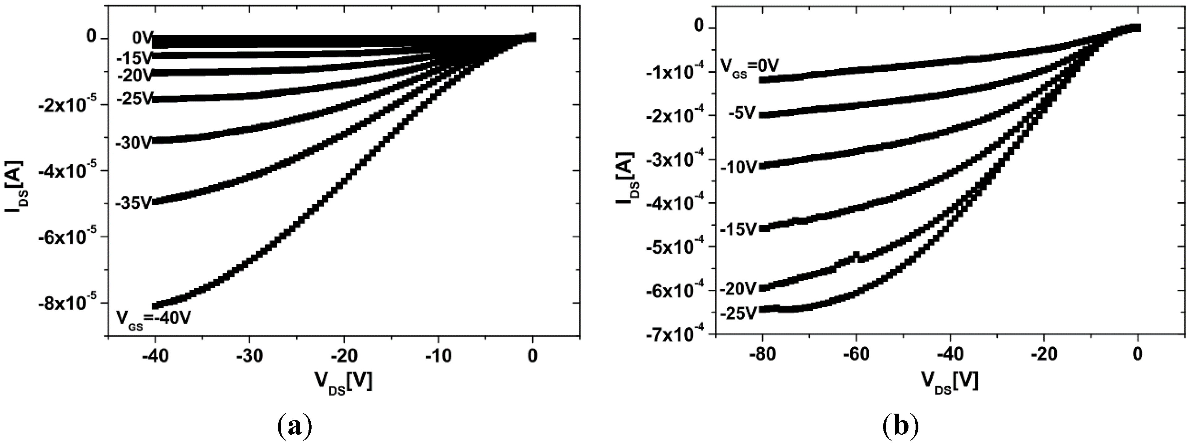
Figure 7 shows the electrical characteristics of an OFET-device using a 200 nm thick high-
k-resist layer as dielectric material. A 150 nm thick aluminum layer serves as the gate electrode. As active semiconducting material, 30 nm of pentacene was thermally evaporated under high-vacuum conditions. The transistor exhibited a threshold voltage of about 7.4 V, an on-off ratio greater than 10
2 and a saturation regime mobility of 0.022 cm
2/Vs [
47].
In general, organic materials are influenced by environmental conditions such as ambient humidity and oxygen. As organic semiconductors act as active layers in OTFT, the device’s performance is directly affected. Water vapor and oxygen lead to modifications in the charge carrier field-effect mobility and in the threshold voltage [
52,
53,
54]. To investigate the impact of ambient humidity and oxygen, long-term experiments were executed. Therefore, an OFET-device using 110 nm of thermally grown SiO
2, as insulating layer, on a heavily doped Si substrate was prepared. A 58 nm thick pentacene layer was evaporated under high-vacuum conditions. The long-term experiments were performed over a period of 9 months at intervals of 3 months. The device was stored under ambient dark atmosphere conditions in a shielded metal box. The measurements were performed under ambient conditions.
Figure 7.
Output characteristics of an inverted coplanar pentacene OTFT using a high-
k dielectric (L = 10 μm, W = 1000 μm and t
ins = 200 nm). Reprinted from [
47], with permission from John Wiley and Sons.
Figure 7.
Output characteristics of an inverted coplanar pentacene OTFT using a high-
k dielectric (L = 10 μm, W = 1000 μm and t
ins = 200 nm). Reprinted from [
47], with permission from John Wiley and Sons.
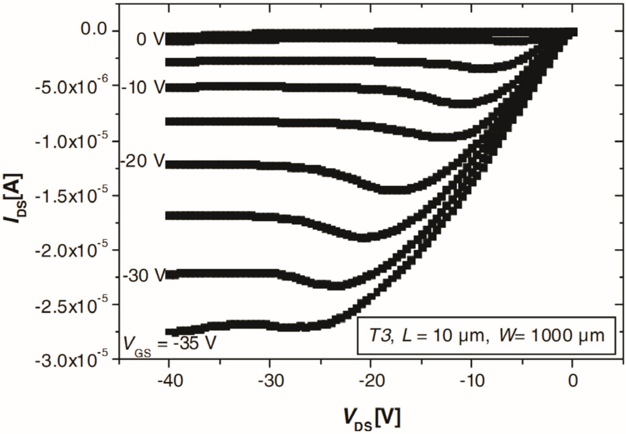
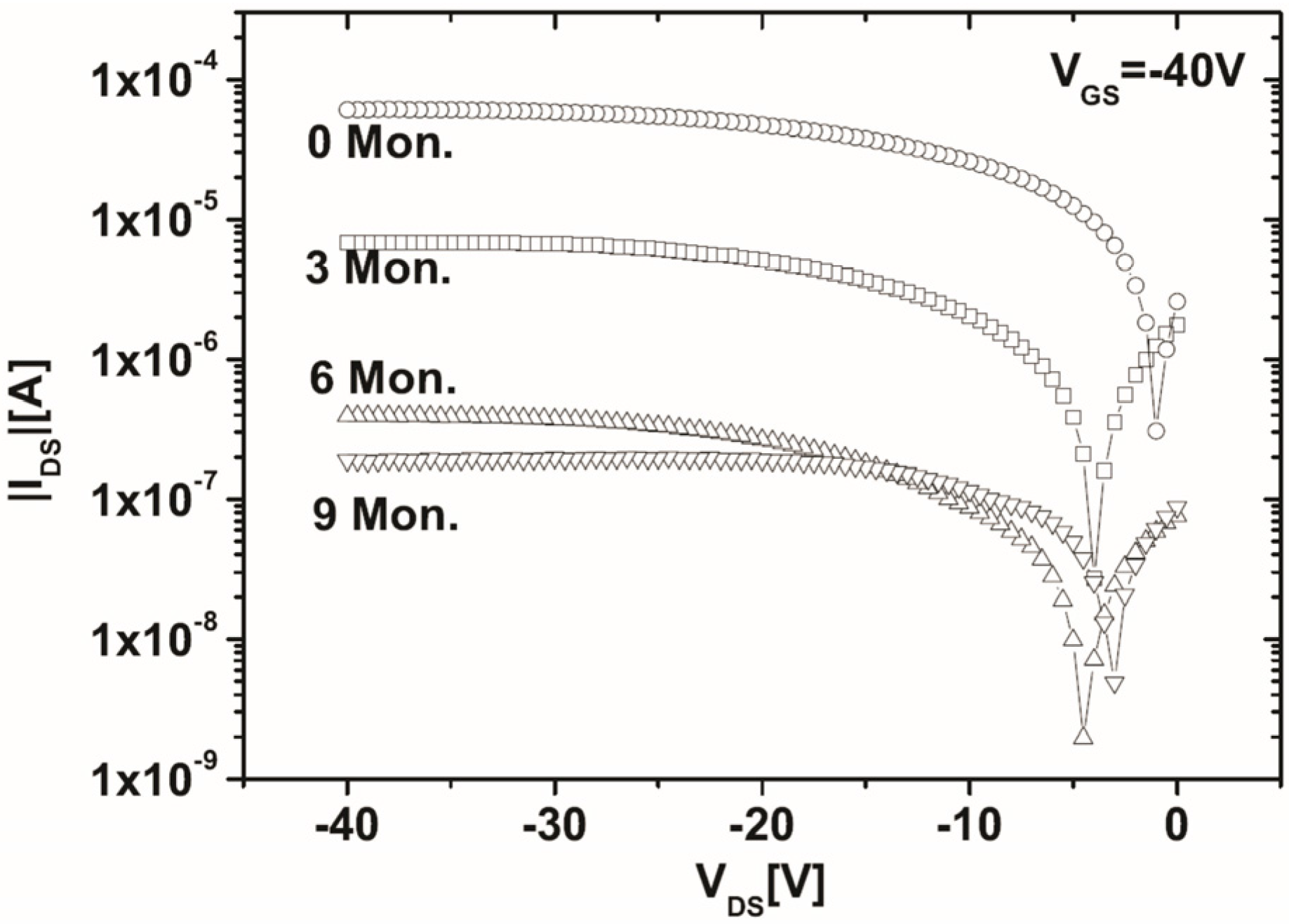
Figure 8 shows the electrical characteristics of the device during the long-term experiment. Over the 9 months interval, the drain current decreases from −61 µA to −187 nA, the charge carrier mobility in the linear regime diminishes from 2 × 10
−3cm
2/Vs to 1.2 × 10
−5cm
2/Vs, and the threshold voltage shifts from 4.8 V to −8 V [
55].
Table 1 shows an overview of the results. Further experiments specify the dominating agent in the device’s degradation. Therefore, a chip carrying a proceeded OTFT template was bonded and connected to the measurement setup, followed by placement in a vacuum chamber. A 30 nm thick layer of pentacene was evaporated under high-vacuum conditions. Subsequent to the measurement under high-vacuum conditions, the chamber was flooded with pure technical oxygen before repeating the measurement. The relevant transfer characteristics are shown in
Figure 9.
Figure 8.
V
DS—I
DS characteristics of an inverted coplanar pentacene OTFT at V
GS = −40 V using SiO
2 as gate dielectric after 0, 3, 6 and 9 months (L = 1 µm, W = 1000 µm and t
ox = 110 nm). Reprinted from [
55], with permission from Cambridge University Press.
Figure 8.
V
DS—I
DS characteristics of an inverted coplanar pentacene OTFT at V
GS = −40 V using SiO
2 as gate dielectric after 0, 3, 6 and 9 months (L = 1 µm, W = 1000 µm and t
ox = 110 nm). Reprinted from [
55], with permission from Cambridge University Press.
Table 1.
Behavior of the electrical parameter of an inverted coplanar pentacene OFET-device after 9 months of investigation. Reprinted from [
55], with permission from Cambridge University Press.
Table 1.
Behavior of the electrical parameter of an inverted coplanar pentacene OFET-device after 9 months of investigation. Reprinted from [55], with permission from Cambridge University Press.
| Time | IDS (µA) | Vth (V) | µ (cm2/Vs) |
|---|
| 0 months | −60.9 | 4.8 | 2.0 × 10⁻³ |
| 3 months | −6.8 | 2.3 | 2.4 × 10⁻⁴ |
| 6 months | −0.457 | −3.4 | 2.2 × 10⁻⁵ |
| 9 months | −0.187 | −8 | 1.2 × 10⁻⁵ |
Figure 9.
Transfer characteristics of an inverted coplanar pentacene OTFT using SiO
2 as gate dielectric (L = 1 µm, W = 1000 µm and t
ox = 110 nm). Measurement under vacuum conditions (black curves) and after the impact of oxygen (red curves). © 2015 IEEE. Reprinted, with permission, from [
56].
Figure 9.
Transfer characteristics of an inverted coplanar pentacene OTFT using SiO
2 as gate dielectric (L = 1 µm, W = 1000 µm and t
ox = 110 nm). Measurement under vacuum conditions (black curves) and after the impact of oxygen (red curves). © 2015 IEEE. Reprinted, with permission, from [
56].
Subsequent to the flooding of the chamber, the drain current in the saturation regime decreases from −15.9 µA to −6.4 µA, whereas the threshold voltage shifts from −2.6 V to −0.7 V [
56]. This threshold voltage shift is related to the influence of oxygen on the molecular structure of pentacene. Oxygen is connected to the middle benzene ring of the pentacene molecule, creating acceptor states for electrons [
57]. As a result, negative charges at grain boundaries and at the dielectric surface were introduced [
58]. It should be mentioned that the threshold voltage shifted in the opposite direction as observed in the long term degradation experiments. From the literature it is well-known that water molecules can diffuse into the organic semiconducting material and dissociate under the impact of an electric field [
57]. The formed H
+ and OH
− ions create defects in the pentacene crystal, acting as traps for positive charge carriers. Therefore, the current decreases, the interface between the gate dielectric and the semiconductor becomes polarized and a threshold voltage shift in the negative direction can be observed. It should be mentioned that the sign of the permanent bias stress has an impact on the direction of the threshold voltage shift [
59]. Nevertheless, regarding both experiments, the influence of water seems to dominate the degradation of pentacene OTFT devices. As a result, an efficient encapsulation of pentacene OTFT devices is needed to ensure long term stability. As oxygen also diffuses through polymeric substrates, a flexible encapsulation of the completed device is required.
4. Inorganic-Based TFT
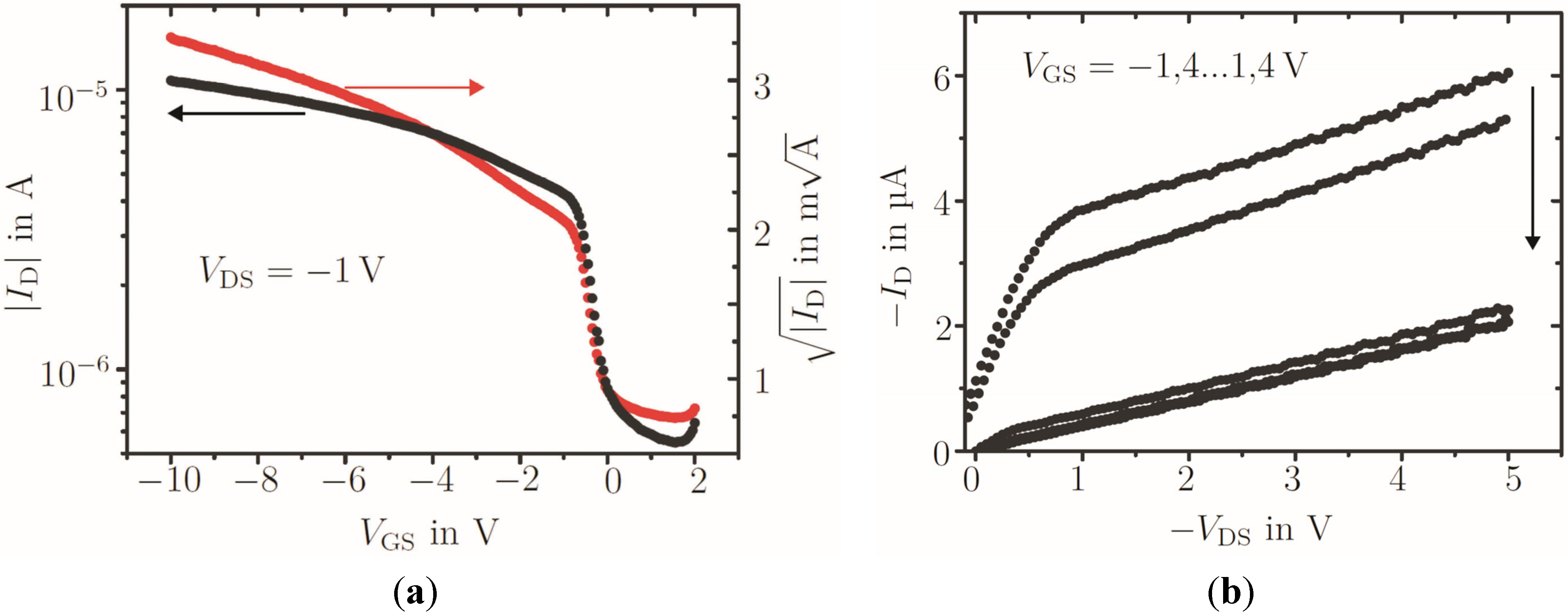
Inorganic semiconductors are commonly more stable than organic semiconductors. For this sake, we investigated the integration of a high-quality inorganic semiconducting layer using low temperature processes for realization of TFTs. For this reason, the use of nanoparticles is a suitable approach to address these issues.
In order to investigate the nanoparticle properties, an oxidized silicon wafer was used as a back contact gate electrode and gate dielectric. Drain and source electrodes were integrated using aluminum. Afterwards, silicon nanoparticles dispersed in ethanol were spin-coated on the substrate. Due to the poor contact between the metal electrodes and the nanoparticles, an annealing step at 500 °C was performed. However, the electrical characteristics of the transistors were poor, and field-effect mobilities of only about 10
−7 cm
2/Vs were extracted [
3]. The main reason for the low performance of these transistors is related to the inter particle connections. Considering that the transistor has a channel length of 8 µm and the Si nanoparticles have an average size of 60 nm, there are at least 130 particles connecting the drain to the source. As a nature oxide is built on the Si nanoparticle surface, the contact resistance between nanoparticles will increase, diminishing the transistor current level even when high voltages are applied. Due to a reoxidation process, the application of a passivation layer or even the removal of the oxide layer by using hydrofluoric acid will not enhance the transistor performance [
60]. Hence, TFTs based on Si nanoparticles are not suitable for device integration on flexible substrates, mainly because of the poor quality of the contacts between the nanoparticles and the high annealing temperatures.
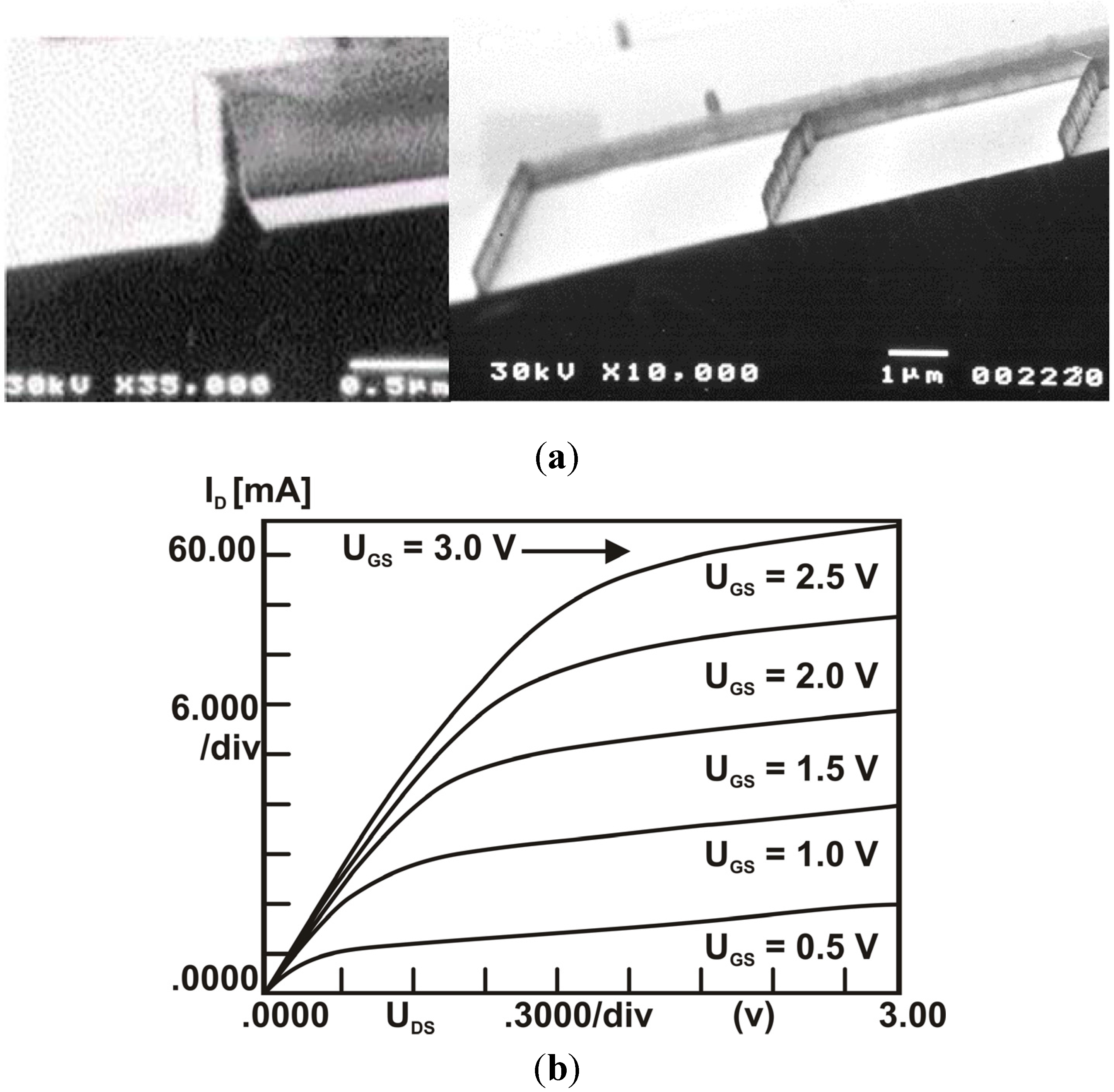
In order to reduce the number of inter-particle connections and to improve transistor performance, a smaller transistor is required. For this sake, the side-wall deposition etch-back technique can be used even with µm-resolution photolithography, as previously discussed. The best performance will be achieved when the transistor channel length perfectly matches the nanoparticle size. In this case, a single nanoparticle acts as the active semiconductor connecting drain and source [
61]. An inverted coplanar setup with L = 60 nm and W = 100 µm was integrated to electrically characterize the transistor.
Figure 10 shows the transistor characteristics. The extracted field-effect mobility, considering the whole transistor width, is about 10
−2 cm
2/Vs [
3]. Nevertheless, due to the low yield of operating devices, the assumption that the entire channel is filled with nanoparticles is not realistic and the mobility is strongly underestimated. A more realistic value, considering that only one nanoparticle is active, is in the range of 100–200 cm
2/Vs [
43].
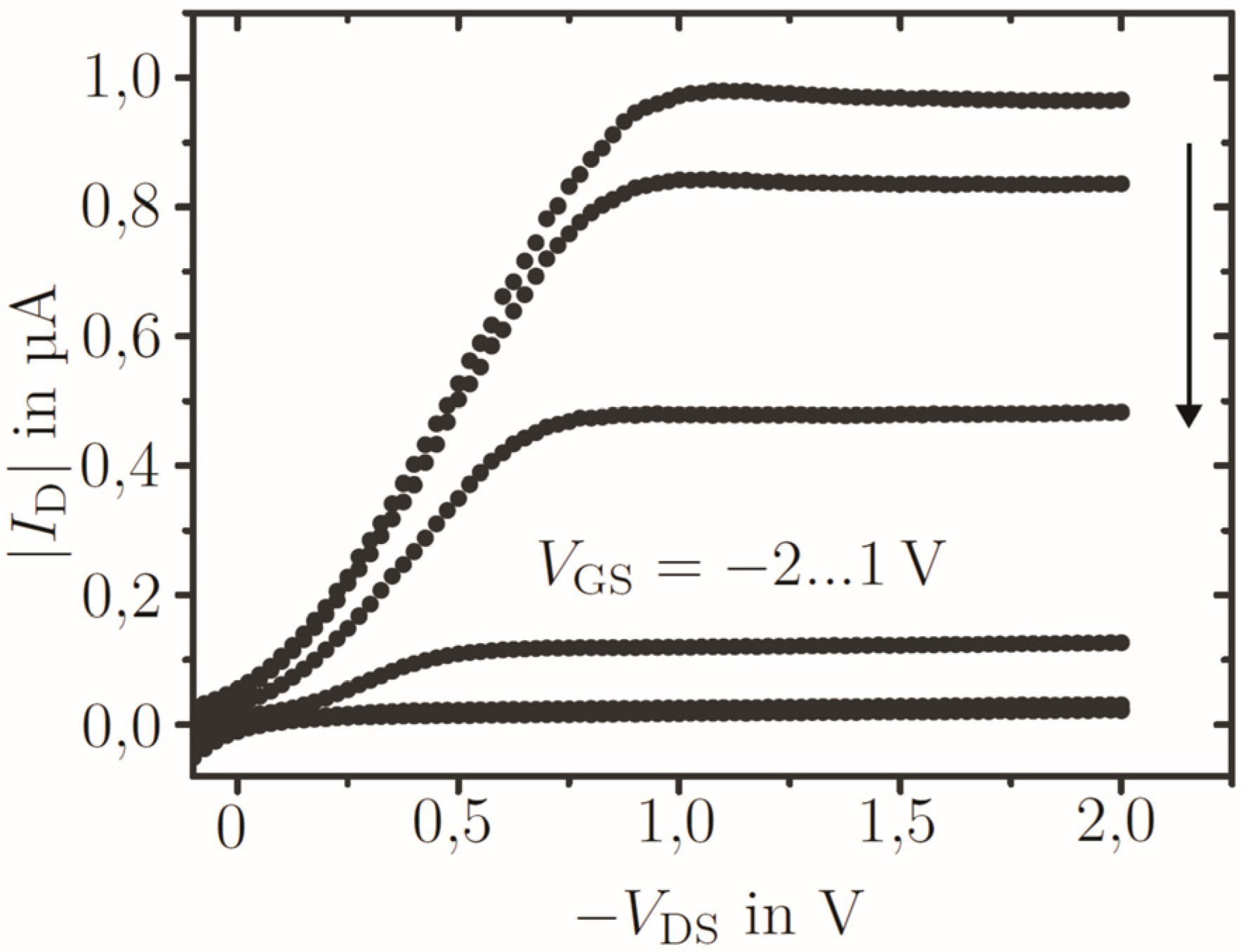
To improve the yield, an inverted staggered setup is used. After the nanoparticle deposition, drain and source electrodes are structured. Even integrating a 70-nm-channel-transistor, the yield is higher and the devices show mobilities of around 10
−3 cm
2/Vs [
3].
Figure 11 depicts a typical output characteristic of these devices. The effect of dopants in the nanoparticle were also investigated, and phosphorous and boron doped nanoparticles were used. On one hand, the influence of phosphorous is weakly observed, because just a few dopants are electrically active. On the other hand, boron doped particles strongly affect the transistor’s behavior, as the aluminum, used as drain and source electrodes, and the p-doped silicon built an ohmic contact [
3].
Figure 10.
(
a) Transfer and (
b) output characteristics of an inverted coplanar single particle TFT integrated by SWEB technique using Si nanoparticles (L = 60 nm, W = 100 µm and t
ox = 15 nm). © 2015 IEEE. Reprinted, with permission, from [
3].
Figure 10.
(
a) Transfer and (
b) output characteristics of an inverted coplanar single particle TFT integrated by SWEB technique using Si nanoparticles (L = 60 nm, W = 100 µm and t
ox = 15 nm). © 2015 IEEE. Reprinted, with permission, from [
3].
Figure 11.
Output characteristics of an inverted staggered single particle TFT integrated by the SWEB technique with a Si nanoparticle (L = 70 nm, W = 800 µm and t
ox = 30 nm). © 2015 IEEE. Reprinted, with permission, from [
3].
Figure 11.
Output characteristics of an inverted staggered single particle TFT integrated by the SWEB technique with a Si nanoparticle (L = 70 nm, W = 800 µm and t
ox = 30 nm). © 2015 IEEE. Reprinted, with permission, from [
3].
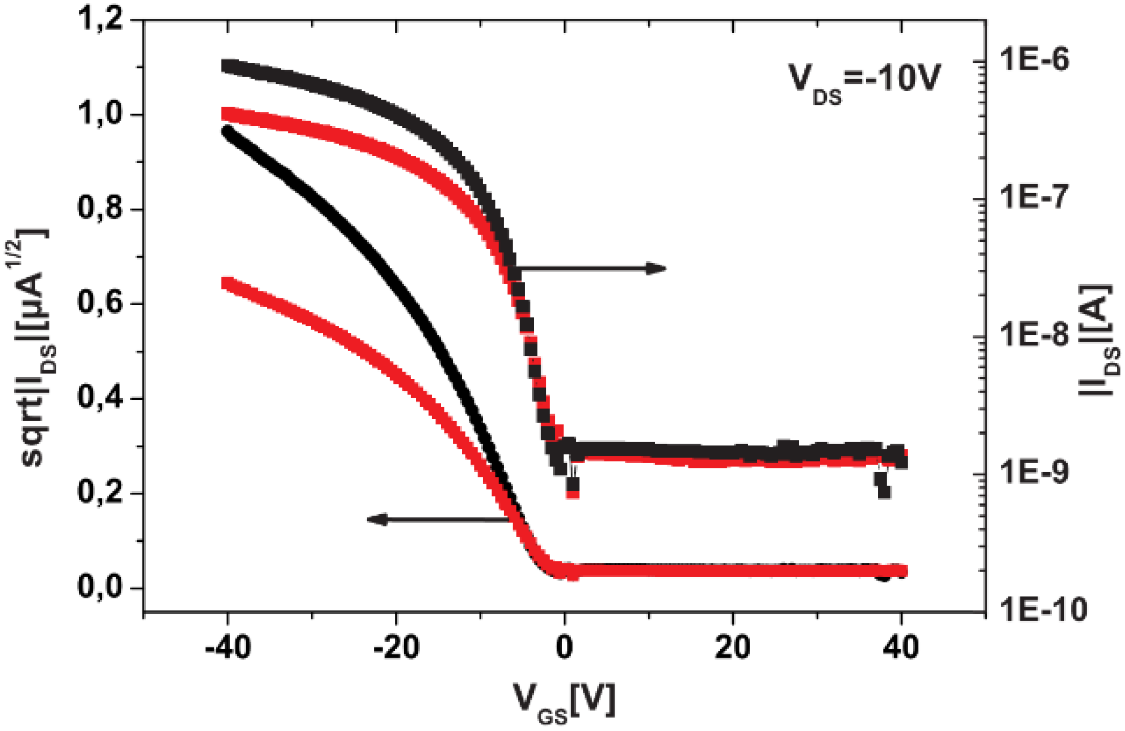
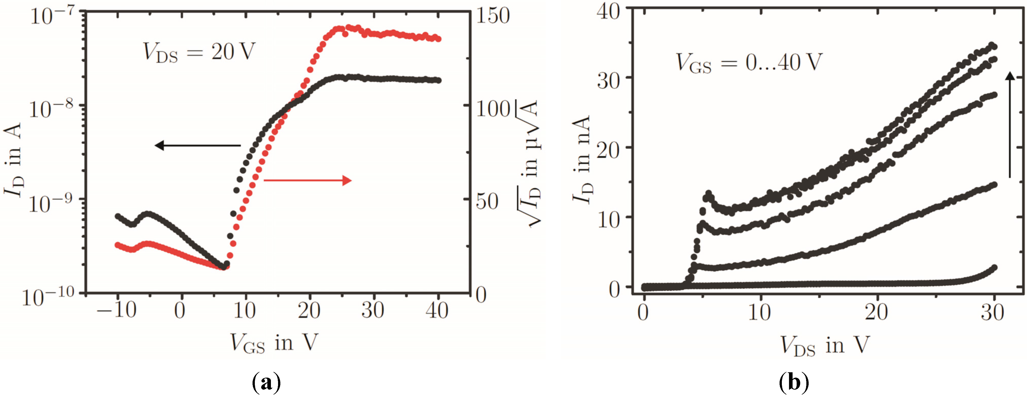
On account of the oxide shell, the performance of TFTs using Si nanoparticles is limited. For this reason, the utilization of a material that does not present an insulating shell is required, for instance a metal oxide. Zinc oxide is a well-researched material, has outstanding electrical, sensory and chemical properties and is transparent to the visible light spectrum. A water-based solution containing ZnO nanoparticles (mean particle size: 80–100 nm) was deposited on templates with metal trenches integrated by the SWEB technique [
62,
63]. As already observed with the single Si nanoparticle TFT, the yield of the operating device is low, mainly because the nanoparticle must perfectly fit the metal gap between the drain and source electrodes. The transfer and output characteristics are depicted in
Figure 12, in which the extracted mobility is around 10
−2 cm
2/Vs considering the whole transistor width. However, due to the low yield of operating devices, it is possible to assume that one or two nanoparticles are responsible for the transistor operation; hence, the mobility would be in the range of 10 to 20 cm
2/Vs [
3,
43].
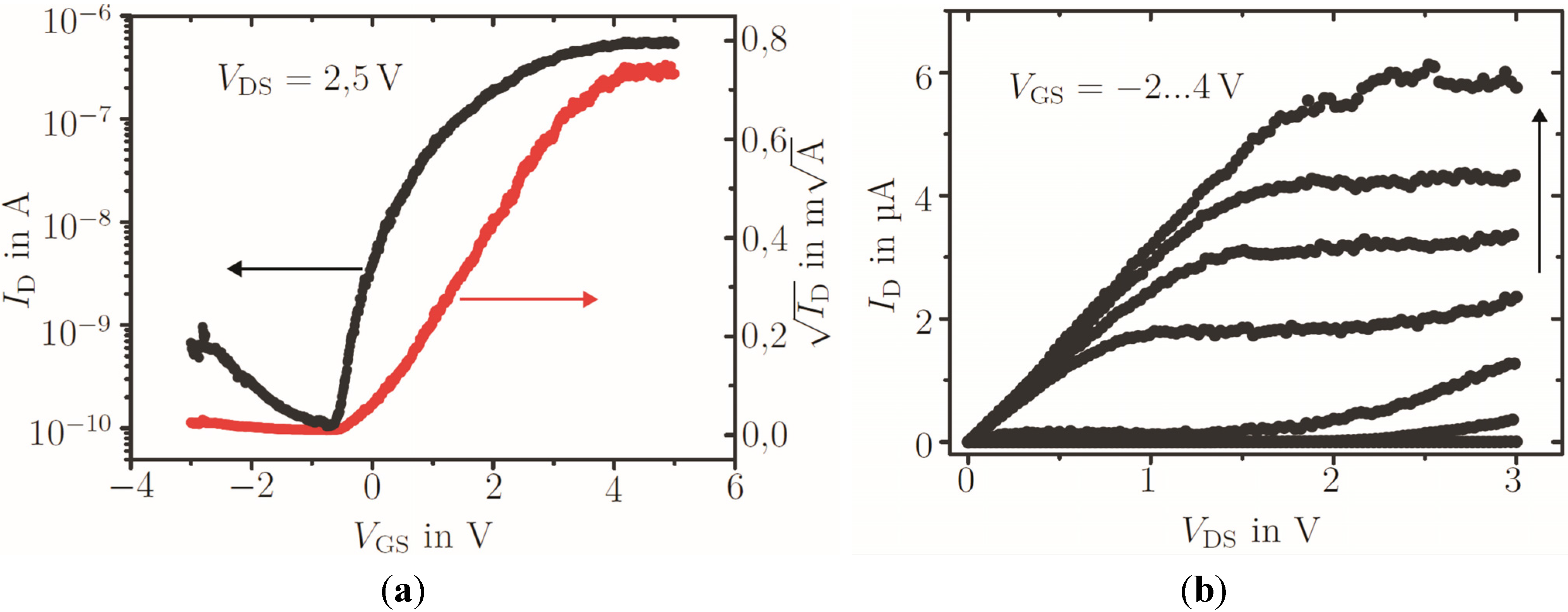
The yield of operating devices can be improved by increasing the metal gap size.
Figure 13 shows a non-inverted staggered setup with channel length of 300 nm. Considering that the mean nanoparticle size is around 80–100 nm, the electron flow will take place through multiple particles. As a result, the maximal on current will be reduced [
43]. Additionally, as a consequence of the top gate structure, the interface between the nanoparticles and the gate dielectric is rough, and a non-uniform accumulation layer in the semiconducting film is formed, reducing the drain current.
Figure 12.
(
a) Transfer and (
b) output characteristics of an inverted coplanar single particle TFT integrated using the SWEB technique with ZnO nanoparticle (L = 80 nm, W = 100 µm and t
ox = 31 nm). © 2015 IEEE. Reprinted, with permission, from [
3].
Figure 12.
(
a) Transfer and (
b) output characteristics of an inverted coplanar single particle TFT integrated using the SWEB technique with ZnO nanoparticle (L = 80 nm, W = 100 µm and t
ox = 31 nm). © 2015 IEEE. Reprinted, with permission, from [
3].
Figure 13.
Output characteristics of a noninverted staggered ZnO nanoparticle TFT integrated by SWEB technique (L = 300 nm, W = 20 µm and t
ox = 120 nm). © 2015 IEEE. Reprinted, with permission, from [
43].
Figure 13.
Output characteristics of a noninverted staggered ZnO nanoparticle TFT integrated by SWEB technique (L = 300 nm, W = 20 µm and t
ox = 120 nm). © 2015 IEEE. Reprinted, with permission, from [
43].
As the ZnO nanoparticle-based devices showed reasonable electric characteristics and the yield of well-operating devices was higher, the ZnO nanoparticle dispersion was spin-coated on a similar inverted coplanar template as that used for Si nanoparticles. After an annealing step of 430 °C in an oxygen atmosphere to saturate the oxygen vacancies in the lattice, the transistors were characterized. As shown in
Figure 14, the transistors depict improved performance in comparison to the Si nanoparticle transistor. Nonetheless, due to the poor contact between the nanoparticles and the drain/source metal electrodes, the on-current is limited and a field-effect mobility about 10
−5 cm
2/Vs was produced [
3]. As discussed previously, the contact between the semiconductor and the metal electrode can be improved by an inverted staggered setup. However, because of the limited adhesion between the nanoparticulated film and the silicon oxide (gate dielectric), an additional thermal treatment is required. The annealing step was performed at 600 °C in an oxygen atmosphere, where a sintering process in the nanoparticulated film was observed and the adhesion was improved [
3,
64].
Figure 15 shows the typical transfer and output characteristics of a ZnO TFT when a staggered setup is used. The expected increase of the on-current is observed and a mobility in the order of 10
−3 cm
2/Vs was extracted, as well as an improved on-off ratio of around 10
4 [
3]. Due to the high process temperature used during the fabrication of this device, they are not suitable for flexible electronics.
Figure 14.
(
a) Transfer and (
b) output characteristics of an inverted coplanar ZnO nanoparticle TFT (L = 8 µm, W = 16000 µm and t
ox = 300 nm). © 2015 IEEE. Reprinted, with permission, from [
3].
Figure 14.
(
a) Transfer and (
b) output characteristics of an inverted coplanar ZnO nanoparticle TFT (L = 8 µm, W = 16000 µm and t
ox = 300 nm). © 2015 IEEE. Reprinted, with permission, from [
3].
Figure 15.
(
a) Transfer and (
b) output characteristics of an inverted staggered ZnO nanoparticle TFT (L = 8 µm, W = 16000 µm and t
ox = 53 nm). © 2015 IEEE. Reprinted, with permission, from [
3].
Figure 15.
(
a) Transfer and (
b) output characteristics of an inverted staggered ZnO nanoparticle TFT (L = 8 µm, W = 16000 µm and t
ox = 53 nm). © 2015 IEEE. Reprinted, with permission, from [
3].
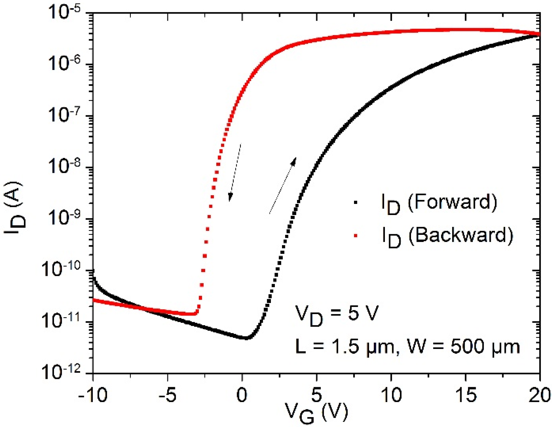
The integration of TFTs using a silicon substrate as a gate back contact is adequate to investigate the transistor performance and characteristics of the semiconductor/metal interface. However, for the integration of electronic circuits, the definition of the gate electrode is required. Aiming a later fabrication on foils, a flexible gate dielectric must be used. For this reason, a polymeric dielectric,
i.e., a 5:1:51 PVP:PMCF:PGMEA mixture, was evaluated [
65,
66]. An annealing step at 200 °C is required to initiate the polymer cross-linking reaction.
Figure 16 depicts the transistor transfer curve, where a highly pronounced hysteresis is observed when the gate voltage is swept forward and backward. The hysteresis is mainly attributed to the dipoles which are present in the gate dielectric, and to the interaction with the ambient. A partial cross-linked process, which increases the effect of the hydroxyl groups in the gate dielectric layer, gives rise to these dipoles [
67,
68]. Conjointly, molecular oxygen and adsorbed water at the nanoparticle surface may induce variation in the film carrier concentration [
69,
70]. A more precise and detailed explanation regarding this hysteretic behavior is given in our previous work [
71].
Figure 16.
Transfer characteristics of an inverted staggered ZnO nanoparticle TFT using PVP as gate dielectric (L = 1.5 µm, W = 500 µm and tins = 200 nm).
Figure 16.
Transfer characteristics of an inverted staggered ZnO nanoparticle TFT using PVP as gate dielectric (L = 1.5 µm, W = 500 µm and tins = 200 nm).
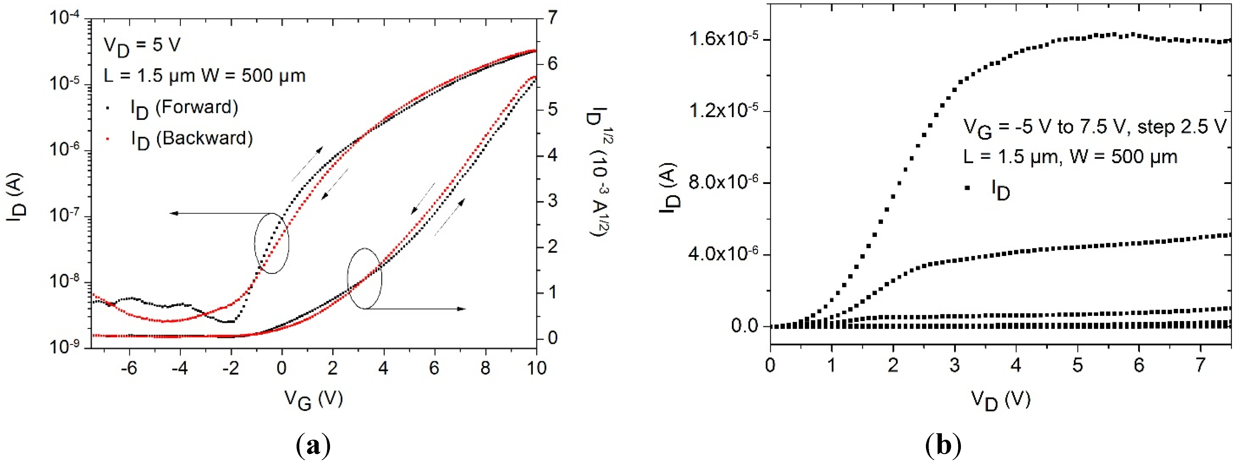
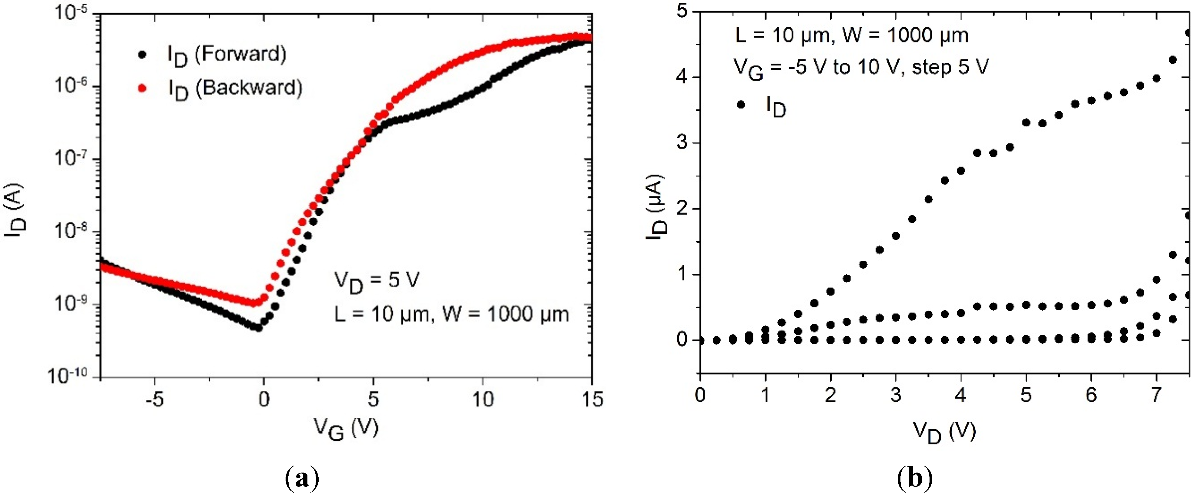
To achieve better performance and reduction of hysteresis, a high-
k dielectric containing TiO
2 nanoparticles can be used. An improved device is achieved, as shown in
Figure 17. A field-effect mobility of around 0.1 cm
2/Vs and a threshold voltage of around 2.2 V were produced [
72]. This integration process is fully compatible with flexible substrates, and the maximum temperature for these devices was only 150 °C.
In order to investigate a later integration on large area foils, a spray coating technique was evaluated for the deposition of the semiconducting film. For this study, an inverted coplanar setup was tested with the maximal processing temperature limited to 150 °C. Due to a capillary effect, the solution containing the ZnO nanoparticles was deposited preferably within the channel area, which improves the yield of devices operating well in comparison to spin-coated devices. A typical transfer and output curve of one of these devices is depicted in
Figure 18. Additionally, oxygen plasma treatment prior to the spray coating deposition and heating up the substrate during the spray step improve the semiconducting film morphology [
73]. This shows that the spray coating technique has good potential for later integration in large-area and flexible substrates.
Figure 17.
(
a) Transfer and (
b) output characteristics of an inverted staggered ZnO nanoparticle TFT using a high-
k dielectric (L = 1.5 µm, W = 500 µm and t
ins = 200 nm). Reprinted from [
72], with permission from Elsevier.
Figure 17.
(
a) Transfer and (
b) output characteristics of an inverted staggered ZnO nanoparticle TFT using a high-
k dielectric (L = 1.5 µm, W = 500 µm and t
ins = 200 nm). Reprinted from [
72], with permission from Elsevier.
Figure 18.
(a) Transfer and (b) output characteristics of an inverted coplanar ZnO nanoparticle TFT using spray coating technique and a high-k dielectric (L = 10 µm, W = 1000 µm and tins = 200 nm).
Figure 18.
(a) Transfer and (b) output characteristics of an inverted coplanar ZnO nanoparticle TFT using spray coating technique and a high-k dielectric (L = 10 µm, W = 1000 µm and tins = 200 nm).
As the electron flow through a ZnO nanoparticulated film is based on percolation paths [
74], traps located at determined current paths will induce a discrete current fluctuation. For this sake, it is possible to observe non-continuities in the I-V curve presented in this study. Additional information about this effect can be found in [
72]. The large surface area present in nanocompounds highlights the effect of the traps [
75], but the same effect may occur for polycrystalline and amorphous films.
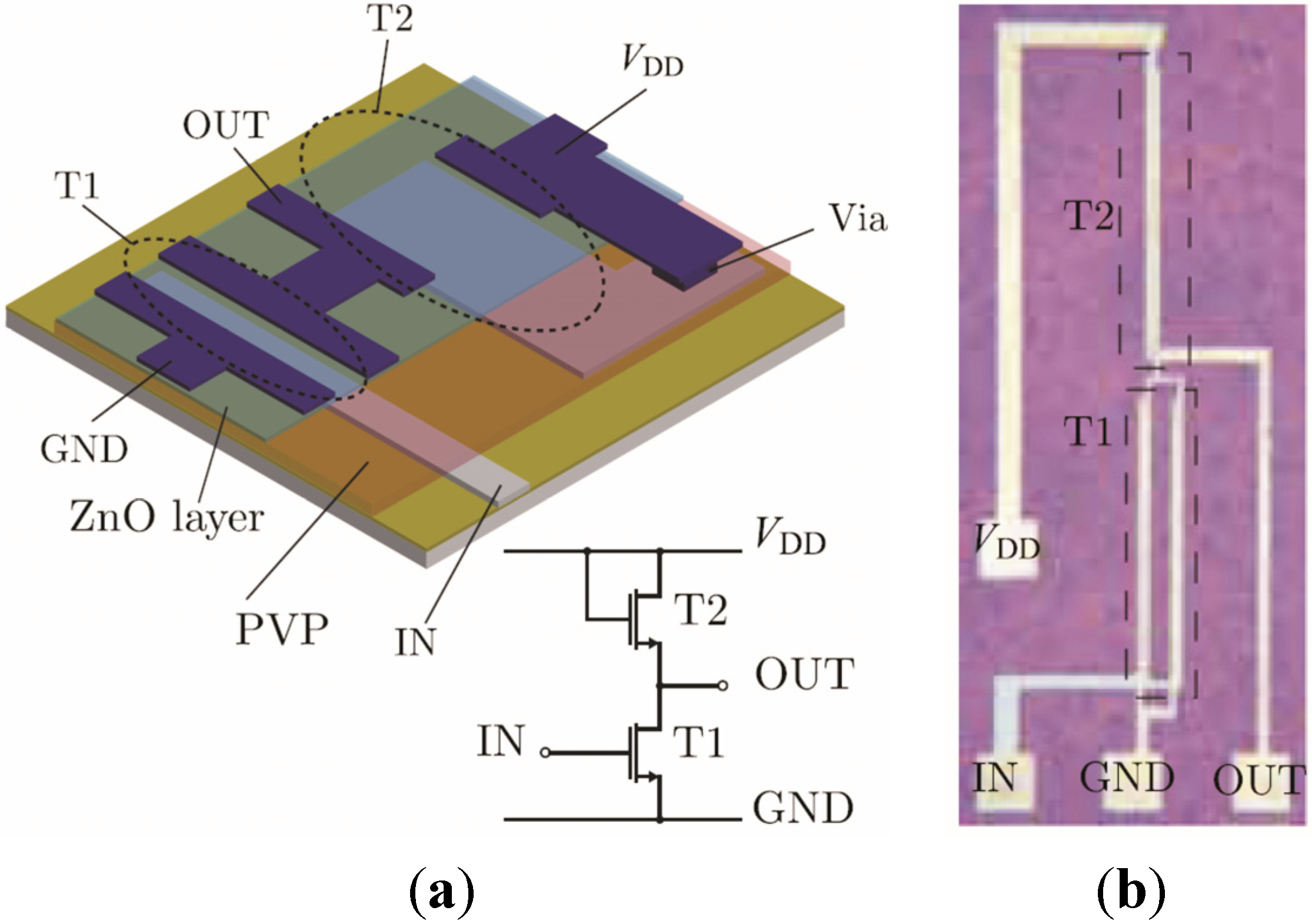
5. First Applications
The electrical characteristics of the integrated TFTs enable the integration of inverter circuits. Additionally, since the integration process was carefully selected to be compatible with flexible substrates, it is possible to transfer the integration process to different kinds of substrates. Glass substrate is commonly used as an intermediate substrate, allowing a smooth transition from an oxidized Si wafer to foils. For the circuit, an enhancement-load inverter was designed.
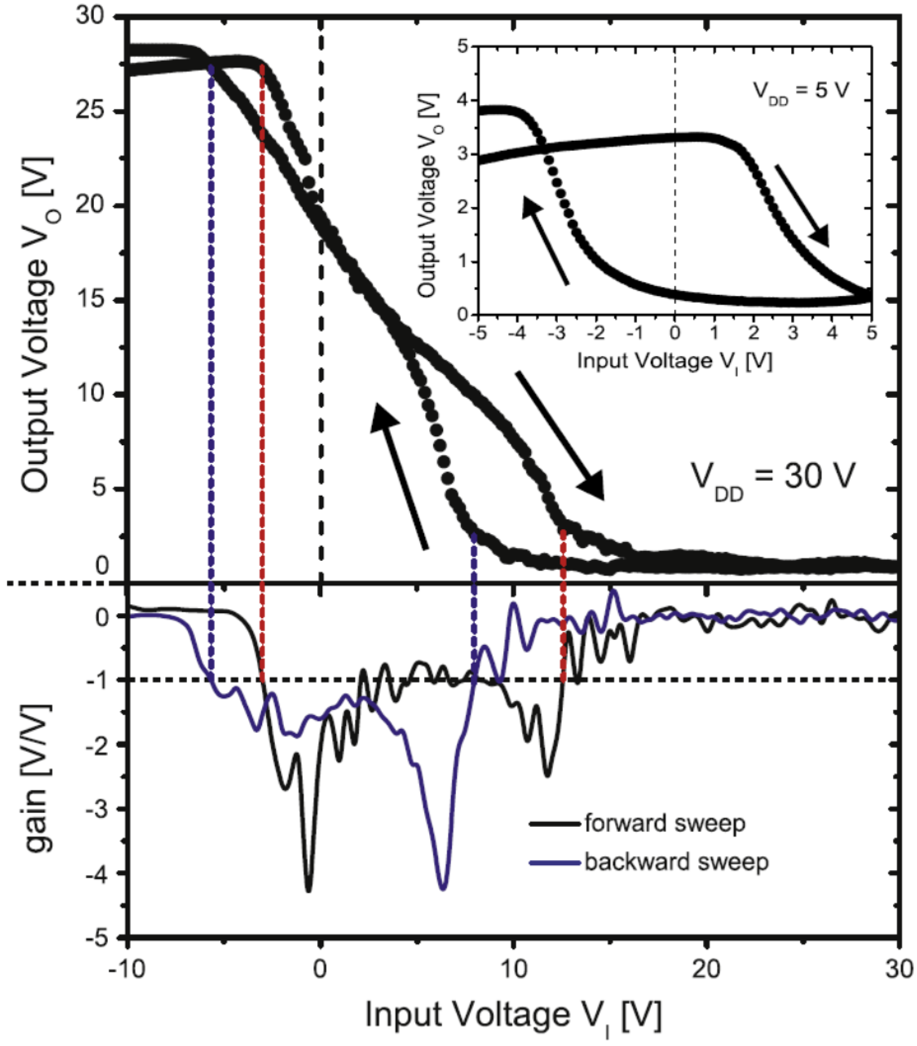
Figure 19a depicts a 3D schematic graph of a ZnO based inverter, as well as its electrical representation.
Figure 19b depicts an optical microscope image of this element. The electrical characteristics of the inverter are presented in
Figure 20. It is possible to observe that the inverter shows maximum peak gains of about 4 V/V and the power dissipation density is less than 26 nW/μm
2 [
76]. The voltage transfer characteristics are affected by the hysteretic behavior when PVP is used as the gate dielectric. Nonetheless, it is demonstrated that ZnO nanoparticles have the potential for digital circuit integration, even when low annealing temperatures are used [
66,
76].
Figure 19.
(
a) Schematic graph, electrical representation and (
b) an optical microscope picture of the inverter. Reprinted from [
66], with permission from Elsevier.
Figure 19.
(
a) Schematic graph, electrical representation and (
b) an optical microscope picture of the inverter. Reprinted from [
66], with permission from Elsevier.
Figure 20.
Voltage transfer characteristics of a ZnO based inverter. Reprinted from [
76], with permission from Elsevier.
Figure 20.
Voltage transfer characteristics of a ZnO based inverter. Reprinted from [
76], with permission from Elsevier.
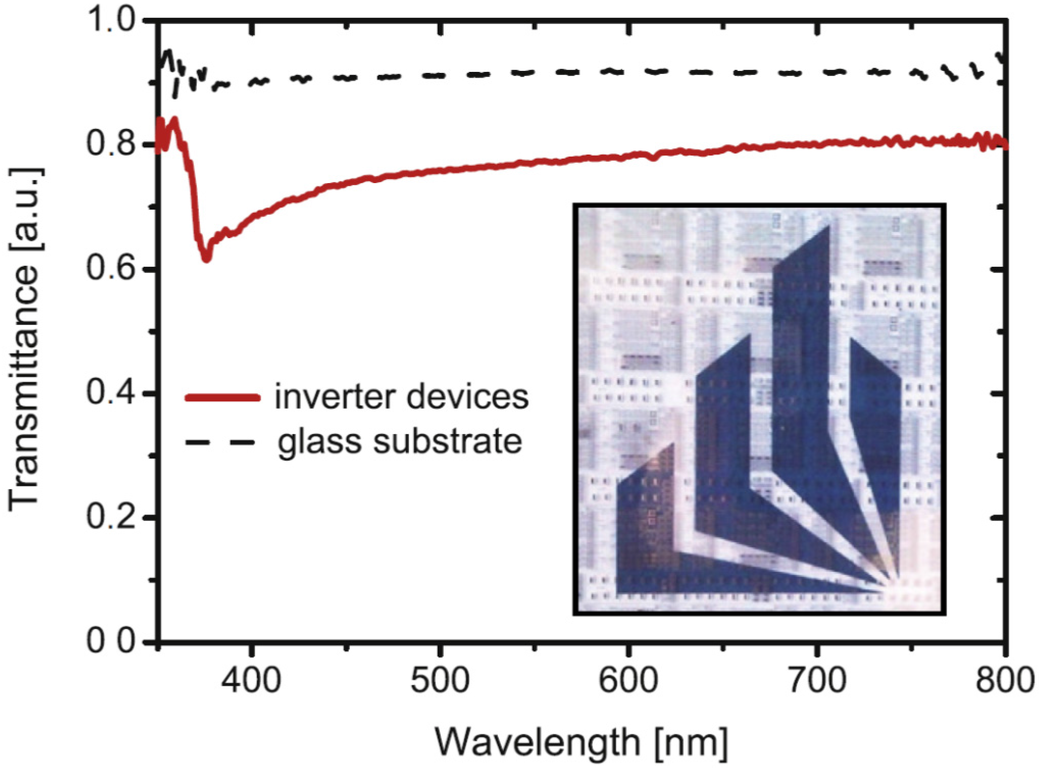
The optical properties of the inverter structure were also investigated.
Figure 21 depicts the optical transmittance of the inverter device in the visible light spectrum. The minimum transmittance at a wavelength of about 370 nm is typical for the ZnO nanoparticles [
77]. Because aluminum was used as contact electrodes (gate, drain and source), the transmittance is furthermore reduced. However, the integrated transistors and circuits are sufficiently transparent.
Figure 21.
Optical transmittance of ZnO based inverter on a glass substrate. Reprinted from [
76], with permission from Elsevier.
Figure 21.
Optical transmittance of ZnO based inverter on a glass substrate. Reprinted from [
76], with permission from Elsevier.
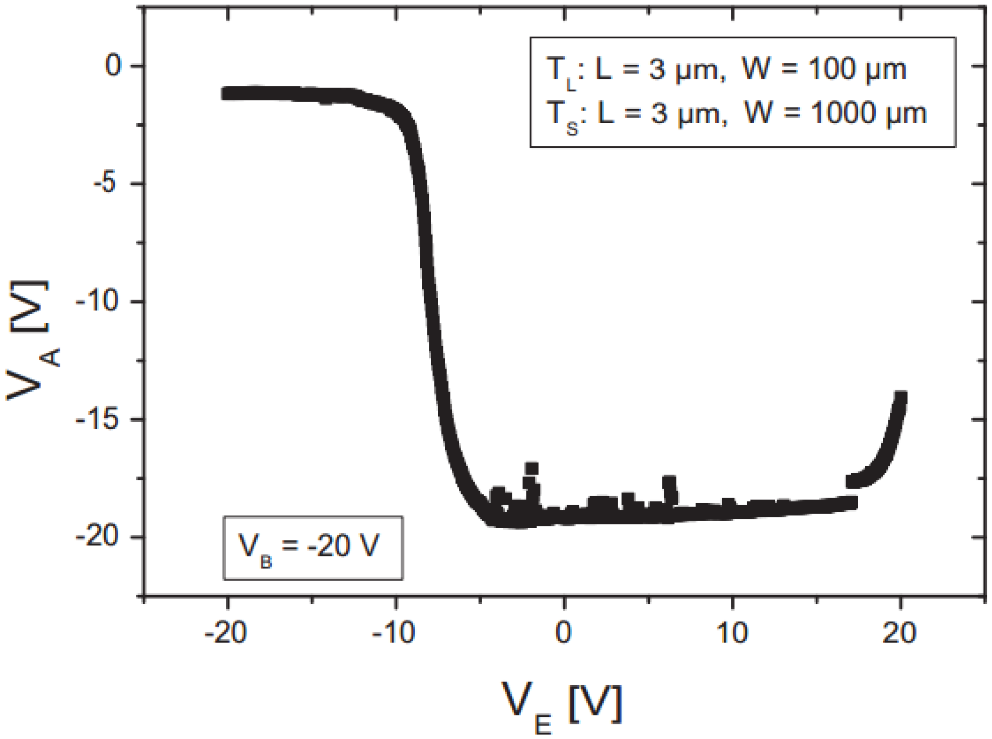
Beside the above exhibit inverter structures, inverters based on pentacene were realized. For the gate electrode 50 nm of gold was evaporated on a silicon substrate. A high-k-resist containing TiO2 as inorganic component (k = 9.5) was deposited by spin-coating, resulting in a layer thickness of 300 nm for the gate dielectric. Gold was used for drain and source contacts. As an active semiconducting layer, 40 nm pentacene was thermal evaporated under high-vacuum conditions.
Figure 22 shows the electrical characteristics of the resulting inverter. Stable high- and low-level and peak gains of about 5.5 V/V demonstrate its applicability in digital circuits [
78].
Figure 22.
Voltage characteristics of a pentacene based inverter using a high-
k dielectric (t
ins = 300 nm) with the output voltage V
A, input voltage V
E and operating voltage V
B. Adapted from [
78].
Figure 22.
Voltage characteristics of a pentacene based inverter using a high-
k dielectric (t
ins = 300 nm) with the output voltage V
A, input voltage V
E and operating voltage V
B. Adapted from [
78].
The previous results related to the high-
k dielectric, as well as low-temperature processing, led to the investigation of OTFTs on foil substrates, as shown in
Figure 23. For the gate electrode, 150 nm of aluminum was evaporated onto a 23 μm PET substrate. The high-
k-resist containing TiO
2 nanoparticles and gold were used as gate dielectric and drain/source contacts, respectively. Before the deposition of the semiconducting layer, the completed template was treated by an oxygen plasma step to improve the molecular order of the growing pentacene film. A 30 nm thick layer of pentacene was deposited under high-vacuum conditions.
Figure 23.
OFET on a PET substrate using a high-
k dielectric. Reprinted from [
47], with permission from John Wiley and Sons.
Figure 23.
OFET on a PET substrate using a high-
k dielectric. Reprinted from [
47], with permission from John Wiley and Sons.
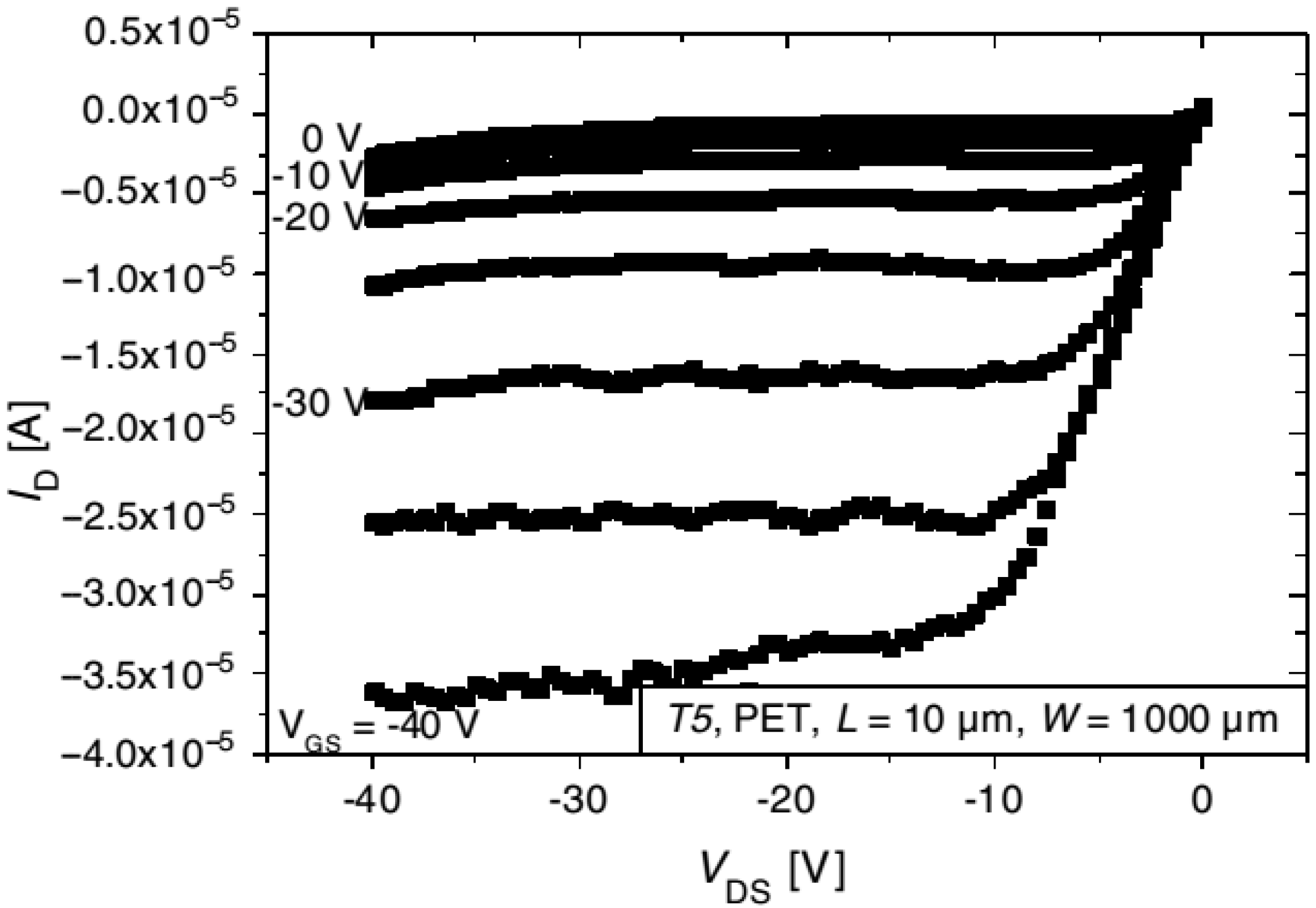
Electrical characteristics of the resulting transistor device are shown in
Figure 24. The maximum drain current is about −36.7 μA at V
DS = −40 V and V
GS = −40 V, whereas the on-off ratio is in the order of 10
3. The threshold voltage is −7.5 V and the charge carrier mobility in the saturation regime is 0.35 cm
2/Vs [
47]. Finally, it should be mentioned that the preparation process can be adjusted to the requirements of ZnO-nanoparticles easily.
Figure 24.
Output characteristics of an inverted coplanar pentacene OTFT using a high-
k dielectric on a PET substrate (L = 10 μm, W = 1000 μm and t
ins = 400 nm). Reprinted from [
47], with permission from John Wiley and Sons.
Figure 24.
Output characteristics of an inverted coplanar pentacene OTFT using a high-
k dielectric on a PET substrate (L = 10 μm, W = 1000 μm and t
ins = 400 nm). Reprinted from [
47], with permission from John Wiley and Sons.
Although the chosen materials and processes are essential to achieve the integration of flexible electronics, flexibility tests are also required to evaluate the effects on device performance. To determine the influence of compression or tensile strain on the electrical properties of TFTs, a systematic change of the bending radius during the electrical characterization has to be carried out. In general, compression or tensile strain causes reversible variations in the channel conductivity until a critical bending radius is reached, and the device is damaged by crack formation in the dielectric layer and delamination of the electrodes [
79,
80]. An enhancement of the flexibility properties can be achieved either by reducing the substrate thickness or an encapsulation of the TFTs in a sandwich construction between a sealant and the substrate [
80]. Recently, Sekitani
et al. showed a low-voltage organic transistor fabricated on a 12.5 μm thick polymeric substrate covered with an encapsulation stack. The device operated without degradation even at a bending radius of 100 μm [
81]. In addition, the gate dielectric influences the device performance as the induced strain modifies the capacitances of the dielectric due to changes in the layers thickness (Poisson-effect) and permittivity.
The electrical properties of materials such as ZnO with a high piezoelectric tensor are influenced when subjected to mechanical stress. Kim
et al. reported a flexible ZnO transistor using atomic layer deposition. Additionally, the variation in the electrical characteristics in different bending states was discussed and attributed to the ZnO piezoelectric properties [
82]. Using a nanoparticular ZnO dispersion, the mechanical stress endured by the transistor during bending states is not transferred to individual nanoparticles. The deformation is instead released through the nanoparticle network. Therefore, the TFT threshold voltage is constant during the bending test; however, the deformation of the ZnO film causes a variation of the physical distance between nanoparticles, which influences the transistor current level, as reported by Jun
et al. [
35].
For organic materials, several results indicate that the electrical properties are influenced by morphological changes in the organic film. Recently, Cosseddu
et al. showed, by a systematical variation of the pentacene crystal domain size, a modification of the hopping energy barrier for the charge carriers [
83]. For instance, as the compression strain shortens the distance between nearby crystal domains, the field-effect mobility is increased.
6. Conclusions
In this article, we discussed the integration processes of (in)organic-based TFTs on foil substrates. As foil substrates are only partially resistant against chemicals and have strict thermic restrictions, the choice of the process parameter is essential. In order to integrate submicron structures on transparent substrates, such as glass or foils, the SWEB technique is a good approach.
For inorganic semiconducting material, Si and ZnO nanoparticle dispersions were evaluated. On the one hand, Si nanoparticulated films are unsuitable for flexible electronics. A low maximum current and a low carrier mobility due to the surrounding oxide shell at the nanoparticle surface were observed. To improve transistor performance, inter-particle connections can be minimized by reducing the transistor’s channel length. On the other hand, ZnO nanoparticles are a promising candidate for integration in low-cost devices. Additionally, they are suitable for large-area substrates when applied using spray-coating techniques.
For the organic semiconductor, evaporated pentacene was the main material used to evaluate the performance of OTFTs. Compared with inorganic semiconductors, pentacene suffers from environmental influences such as ambient humidity and oxygen. Both impacts lead to a reduction of the charge carrier mobility and a threshold voltage shift depending on the specific influencing agent. Long-term experiments show that the dominating effect of the pentacene degradation is related to water vapor.
Furthermore, possible dielectric materials were investigated. Inorganic dielectric materials exhibit either high processing temperatures or insufficient mechanical flexibility. Therefore, polymeric and inorganic-organic nanocomposite (high-k) dielectrics were established. As the used polymeric dielectrics either suffer from solvents used by optical lithography or introduce instabilities during transistor operation, future research efforts will focus on the use of the high-k-resist as dielectric material.
Inverters based on ZnO nanoparticles integrated on a glass substrate were realized. Peak gains of about 4 V/V and a low power consumption were observed. Nevertheless, they are affected by the hysteretic behavior when PVP is used as a gate dielectric. Pentacene and the high-k-resist were used for realization of inverters on Si-substrates and integration of TFTs on PET substrates. For the inverters, a stable low- and high-level as well as a peak gain of 5 V/V were observed. The OTFTs exhibited a threshold voltage of −7.5 V and an on-off ratio in the order of 103. The charge carrier mobility in the saturation regime was found to be 0.35 cm2/Vs.
Future works will focus on two main parts, the improvement of the active semiconducting layer and the reduction of parasitic capacitances. To minimize degradation processes for long term applications, organic semiconductors, as Cn-DNTT or C8-BTBT, promising good environmental stability, will be used, as well as a combination of humidity and UV-irradiation treatment for stabilization and performance enhancement of the ZnO films. Furthermore, the reduction of the overlap of the drain/source contacts with the gate electrode will lead to a diminution of parasitic capacitances increasing the operation frequency. Additional improvement could be achieved when the semiconductor material is limited to the active transistor areas.


