Review

Conduction Mechanism of Valence Change Resistive Switching Memory: A Survey

Faculty of Electrical Engineering, Universiti Teknologi Malaysia, Skudai, Johor 81310, Malaysia
*
Author to whom correspondence should be addressed.
Electronics 2015, 4(3), 586-613; https://doi.org/10.3390/electronics4030586
Submission received: 6 August 2015 / Revised: 25 August 2015 / Accepted: 6 September 2015 / Published: 9 September 2015

Abstract

:
Resistive switching effect in transition metal oxide (TMO) based material is often associated with the valence change mechanism (VCM). Typical modeling of valence change resistive switching memory consists of three closely related phenomena, i.e., conductive filament (CF) geometry evolution, conduction mechanism and temperature dynamic evolution. It is widely agreed that the electrochemical reduction-oxidation (redox) process and oxygen vacancies migration plays an essential role in the CF forming and rupture process. However, the conduction mechanism of resistive switching memory varies considerably depending on the material used in the dielectric layer and selection of electrodes. Among the popular observations are the Poole-Frenkel emission, Schottky emission, space-charge-limited conduction (SCLC), trap-assisted tunneling (TAT) and hopping conduction. In this article, we will conduct a survey on several published valence change resistive switching memories with a particular interest in the I-V characteristic and the corresponding conduction mechanism.

Graphical Abstract

1. Introduction

Floating gate (FG)-based Flash memory devices have been the most prominent nonvolatile memories (NVM) because of high density and low fabrication cost. However, Flash memories continue to suffer from low endurance, low write speed and high voltage in write process [1,2]. Under the circumstances, the resistive switching memory which based on resistance change modulated by electrical stimulus, has inspired both scientific and commercial interest due to its excellent area compaction (4F2, where F is minimal feature size), high switching speed (<100 ps) [3], high endurance (>1012 cycles) [4], good retention (>10 years@85°) [5,6,7,8] and low power consumption (~1 µW) [9]. Numerous theoretical models and experiments have been proposed to explain the resistive switching behavior in various materials ranging from rare-earth oxides (e.g., YCrO3 [10] and LaLuO3 [11]), phase-change chalcogenides (e.g., Ge2Sb2Te5), solid-state electrolytes (e.g., Au/Cu in GeSe) to transition metal oxide (e.g., TiO2 and SrTiO3) [12]. Among these materials, binary transition metal oxides (TMOs) are widely agreed to be the most promising materials [13]. The resistive switching effect can be classified into three categories, namely electrochemical metallization (ECM), thermochemical mechanism (TCM) and valence change mechanism (VCM). ECM is related to metallic (e.g., Ag, Cu) cations migration on solid electrolyte. TCM is related to stoichiometry change in the oxide due to current-induced temperature increase. On the other hand, VCM is triggered by field-assisted oxygen anions migration and valence change of the cation sublattice [14]. Compact modeling of resistive switching memory often consists of three inter-related modules, namely: (i) evolution of CF; (ii) conduction mechanism; and (iii) temperature dynamic evolution [15,16,17,18]. While CF evolution is typically associated with thermal, electrical or ion migration [19,20], there is no consensus on the dominant conduction mechanism in resistive switching memory devices [21,22,23]. Among the commonly observed conduction mechanisms are: (i) Poole-Frenkel emission [24,25,26,27,28,29,30,31,32]; (ii) Schottky emission [33,34,35,36,37,38,39,40,41,42]; (iii) SCLC [43,44,45,46,47,48,49,50,51,52,53] (iv) trap-assisted tunneling [54,55,56,57,58,59]; and (v) hopping conduction [60,61,62,63,64,65]. To enhance the device performance and data retention property, it is crucial to identifying the exact physical transport mechanism and its relation with resistive switching phenomena. Thus, in this article, we conduct a survey on the conduction mechanisms of various VCM based resistive switching memories that reported in the literature. The fundamental of conventional transport mechanisms is described with emphasis on respective current density modeling as well as corresponding electrical field and temperature dependency. We revisit several published works with particular interest in the I-V characteristic and experimental data fitting with conventional conduction expressions. This paper is organized as follows: Section 2 presents an overview of resistive switching memory. Typical conduction mechanisms in resistive switching dielectric film is described in Section 3, and followed with review of observed conduction mechanism in publications in Section 4.

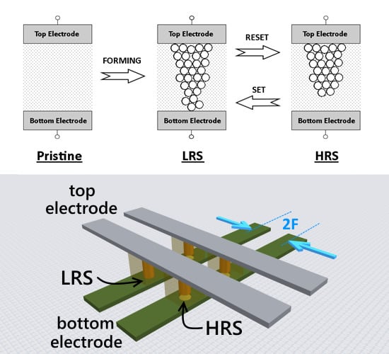
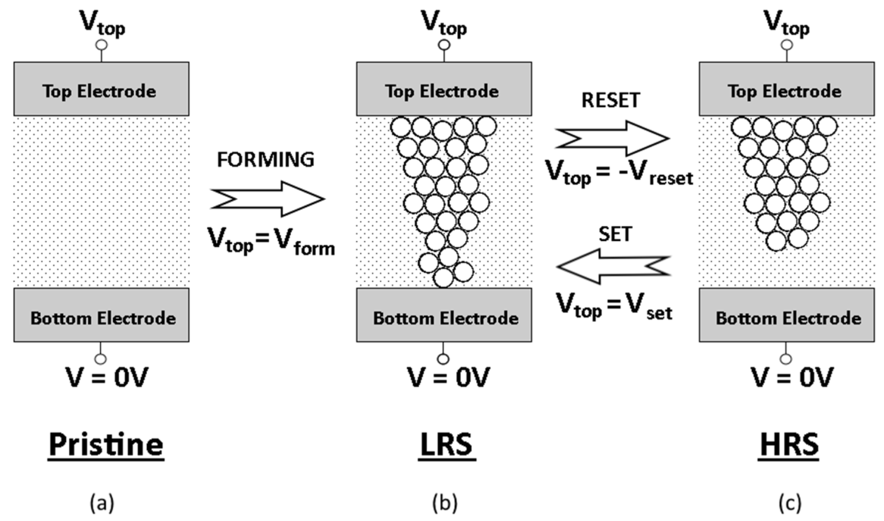
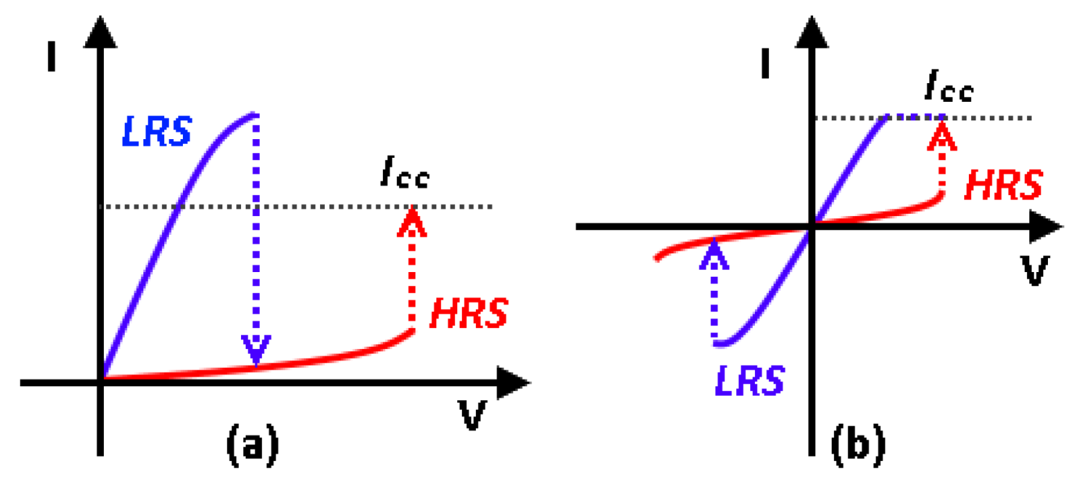
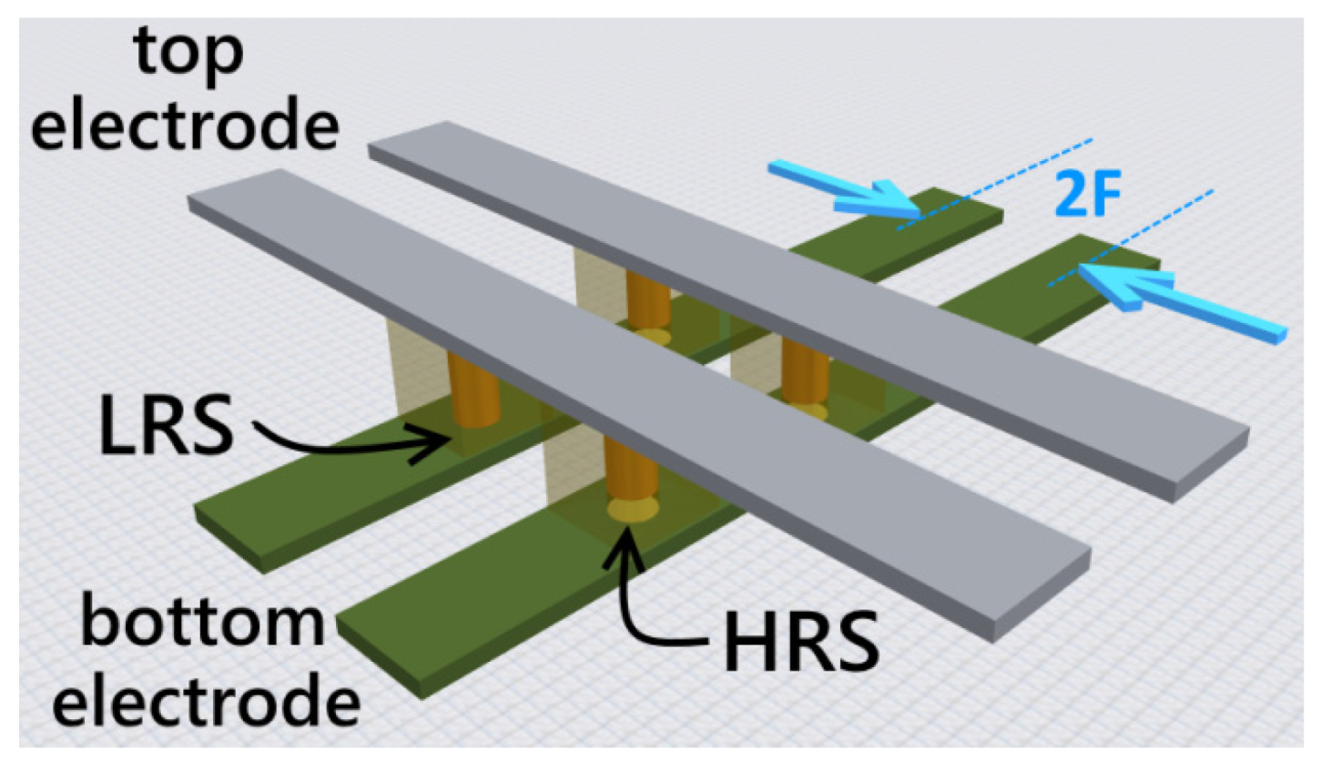
2. Overview of Resistive Switching Memory

Typically, the resistive switching memory is a metal-insulator-metal (MIM) structure built with two metallic electrodes sandwiching an oxide layer. These bistable MIM cells switches back and forth between high resistance state (HRS) and low resistance state (LRS) when an appropriate voltage is applied across the electrodes. This resistance change phenomena is generally attributed to the formation and rupture process of the conductive filament in the oxide as a result of electrode redox reactions and nanoionic transport [66]. Figure 1 illustrates schematic diagram of the switching mechanism in VCM type resistive switching memory.
Figure 1. Schematic of the switching mechanism of bipolar metal oxide resistive switching memory (a) Switching layer in pristine state before electroformed; (b) A low resistance filament is formed when forming voltage is applied to top electrode; (c) The filament is ruptured when a negative voltage is applied and device turns into high resistant state (HRS).
Electronics 04 00586 g001
There are two types of switching mode, namely, unipolar and bipolar. For unipolar, both CF formation and rupture process take place under the same electrical polarity, whereas bipolar requires opposite electrical polarities as shown in Figure 2a,b. Additionally, compliance current (ICC) is often applied to avoid excessive current flow and to prevent the irreversible hard breakdown. Devices with same materials can exhibit different switching mode depending on other factors such as electroforming, doping concentration, stoichiometry and physical parameters [67]. ECM (cation-based) and VCM (anion-based) memories exhibit bipolar switching model, whereas TCM (both cation and anion-based) memory exhibits unipolar switching model [66].
Figure 2. (a) Unipolar; and (b) bipolar switching. ICC is the compliance current to prevent permanent breakdown.
Electronics 04 00586 g002
For high density implementation, resistive switching devices can be arranged in crossbar architecture which has minimum memory cell area of 4F2 [68,69]. Figure 3 shows three-dimensional modeling of a 2-by-2 resistive random access memory (ReRAM or RRAM) implemented in crossbar structure.
Figure 3. Resistive random access memory (RRAM) with resistive switching devices arranged in crossbar architecture.
Electronics 04 00586 g003

3. Typical Conduction Mechanism in Resistive Switching Memory

The electron transport in a MIM structure takes place via series of mechanisms. Some of these conduction mechanisms rely on the electrical property at the electrode-dielectric interface, e.g., energy barrier height of the interface and conduction carriers in dielectric films; the others depend on the properties of the dielectrics itself, e.g., trap level, trap spacing, trap density, carrier drift mobility, dielectric relaxation time and density of states in conduction [70]. Among the electrode-limited conduction mechanisms are (i) Schottky emission; (ii) Fowler-Nordheim (F-N) tunneling; and (iii) direct tunneling. Bulk-limited conduction mechanism includes (i) Poole-Frenkel (P-F) emission; (ii) Ohmic conduction; (iii) SCLC; (iv) ionic conduction; (v) hopping conduction; and (vi) trap-assisted tunneling (TAT).

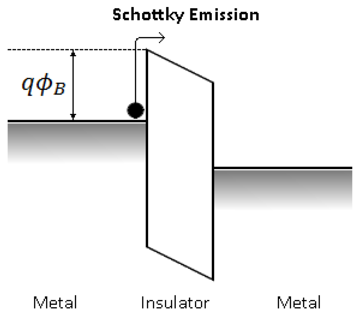
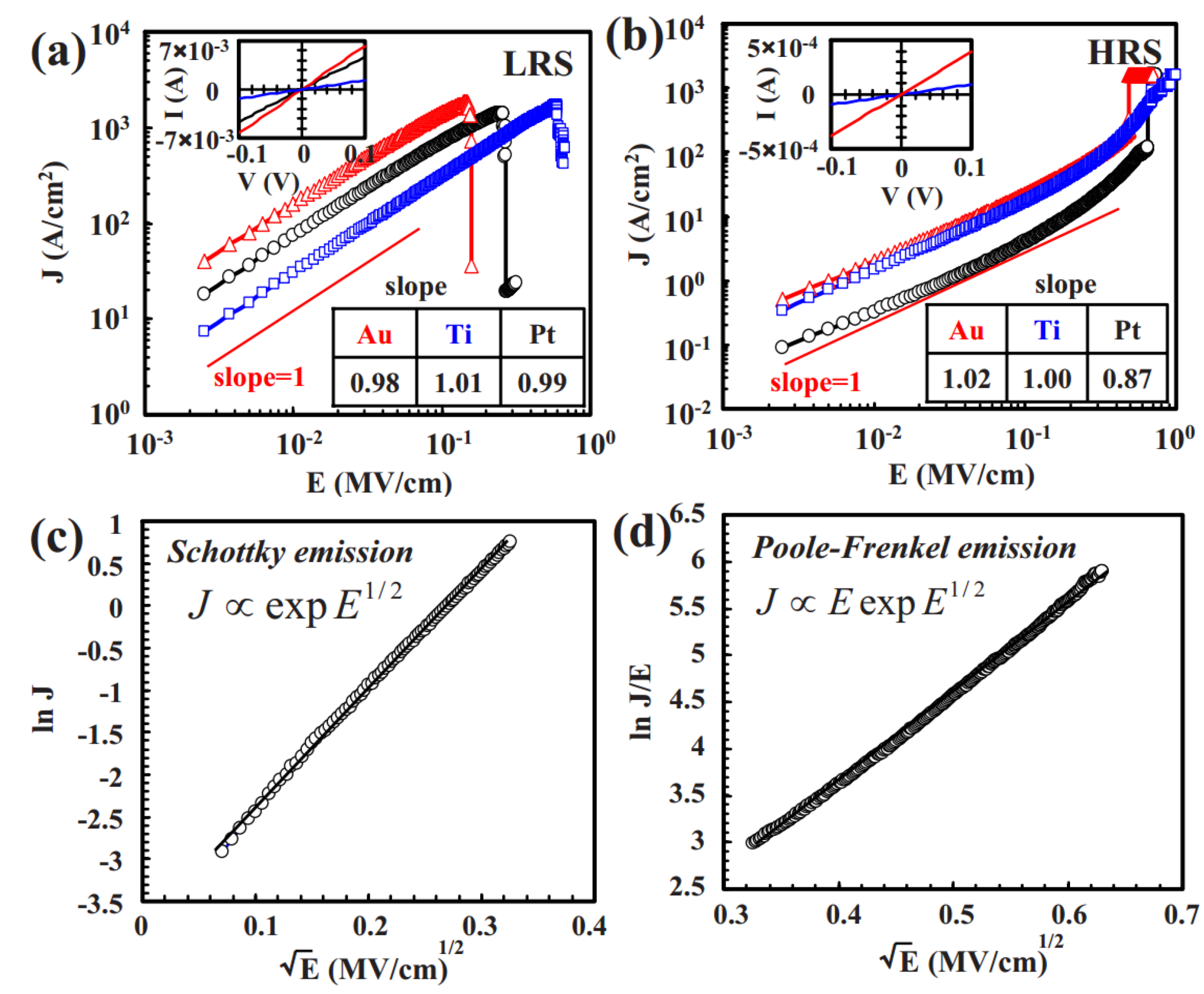
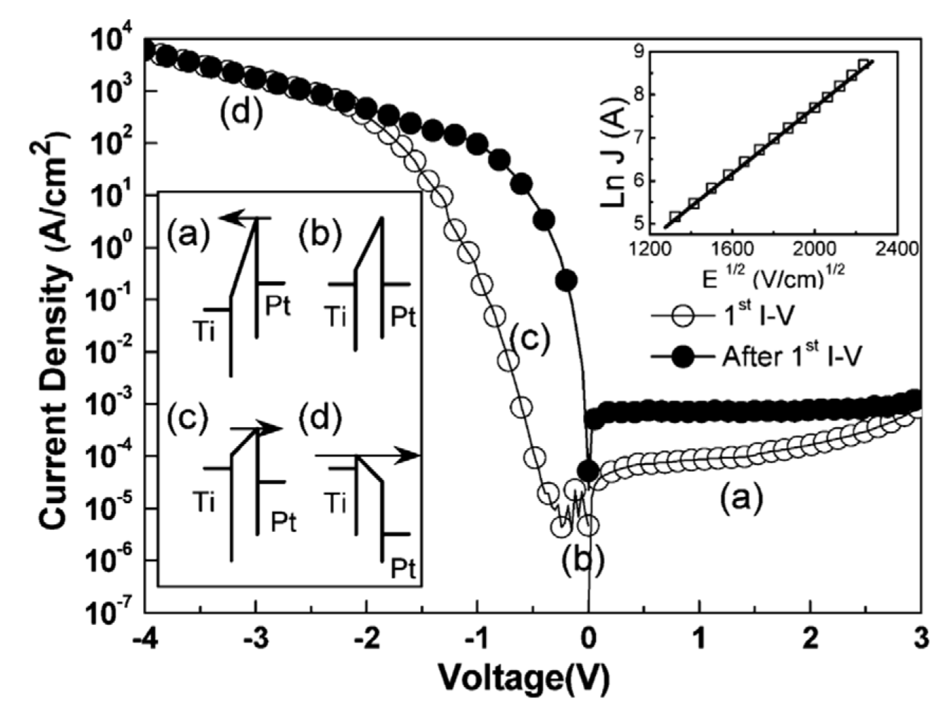
3.1. Schottky Emission

The Schottky or thermionic emission happens when thermally-activated electrons injected over the energy barrier into the conduction band of the oxide as shown in Figure 4 [55]. This type of thermionic emission is one of the most often observed conduction mechanism in oxide especially in relative high temperature [71].
Figure 4. Schematic energy band diagram of Schottky emission in metal-insulator-metal (MIM) structures.
Electronics 04 00586 g004
The current density JSE can be related to electric field (E) and temperature (T) by the Schottky equation as shown in Equation (1).
J S E = 4 π q m * ( k T ) 2 h 3 exp [ q ( ϕ B q E / 4 πε ) k T ]
where m* is the electron effective mass in the oxide, k is Boltzmann’s constant, T is the absolute temperature, h is Planck’s constant, E is the electric field across the oxide, ΦB is the junction barrier height and ε is the permittivity of the oxide. In the case where the mean free path of the electrons is less than the Schottky barrier width, Simmons’ modified Schottky equation (Equation (2)) is more appropriated [72,73].
J S M S E = α T 3 / 2 E μ ( m * m 0 ) 3 / 2 exp [ q ( ϕ B q E / 4 πε ) k T ]
where α is a constant, μ is bulk mobility and m0 is electron mass.

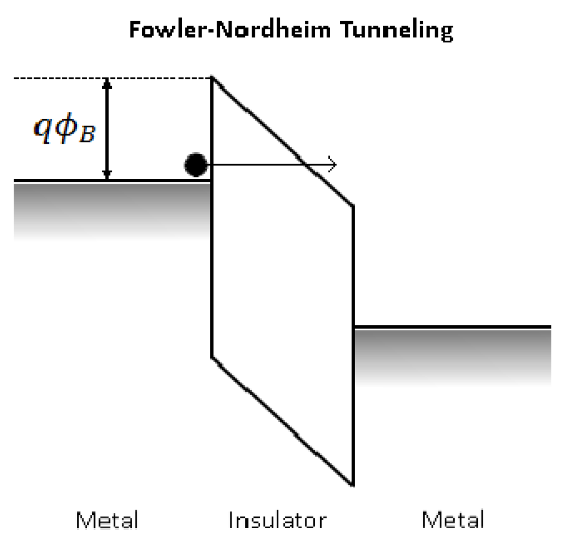
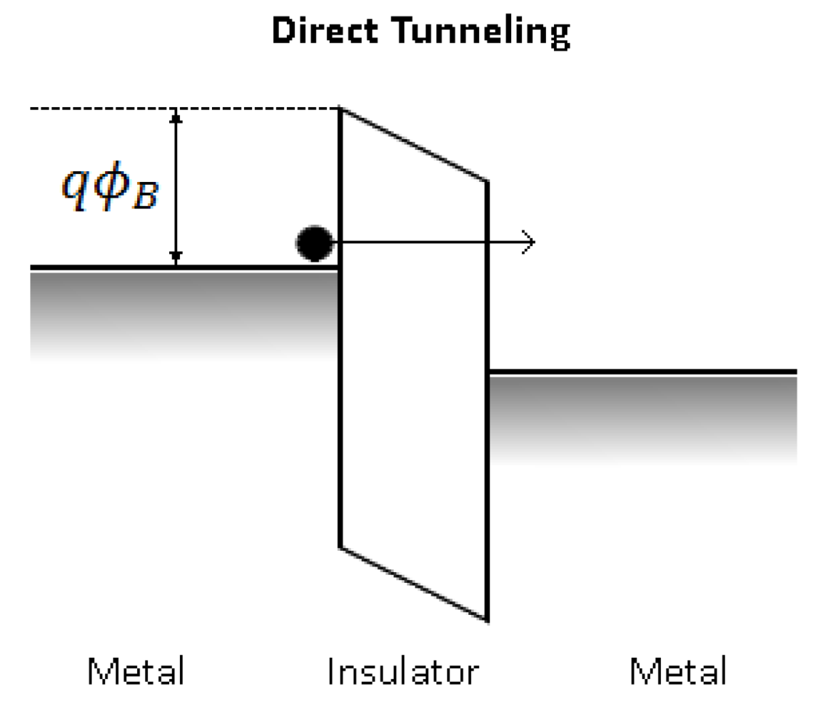
3.2. Fowler-Nordheim (F-N) and Direct Tunneling

In the presence of high electric field, the Fowler-Nordheim (F-N) and direct tunneling across the oxide may take place. Generally, direct tunneling is more dominant in oxide thinner than 3 nm [74], while F-N tunneling is usually more dominant at thicker oxide [71,75] and has been well accepted as charge changing mechanism in floating-gate memory [74]. Figure 5 and Figure 6 show the energy band diagram for F-N and direct tunneling respectively.
The current density due to F-N mechanism can be represented with Equation (3) [76]:
J F N = q 2 8 π h ϕ B E 2 exp ( 8 π 2 q m * 3 h E ϕ B 3 / 2 )
where m* is the electron effective mass in the oxide, h is Planck’s constant, and ΦB is the junction barrier height; whereas, the current density due to direct tunneling can be approximated to Equation (4) [71]:
J D T exp { 8 π 2 q 3 h ( m * ϕ B ) 1 / 2 κ   ·   t o x , e q }
where κ is the relative dielectric constant of the oxide layer and tox,eq is the equivalent oxide thickness (EOT). Note that the current density (JDT) for a given oxide thickness is dependent to the κ value of the dielectric and tunneling barrier height (ΦB) [77].
Figure 5. Energy band diagram for Fowler-Nordheim (F-N) tunneling.
Electronics 04 00586 g005
Figure 6. Energy band diagram for direct tunneling.
Electronics 04 00586 g006

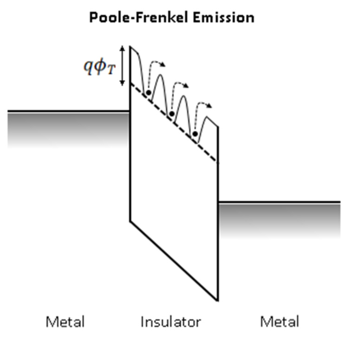
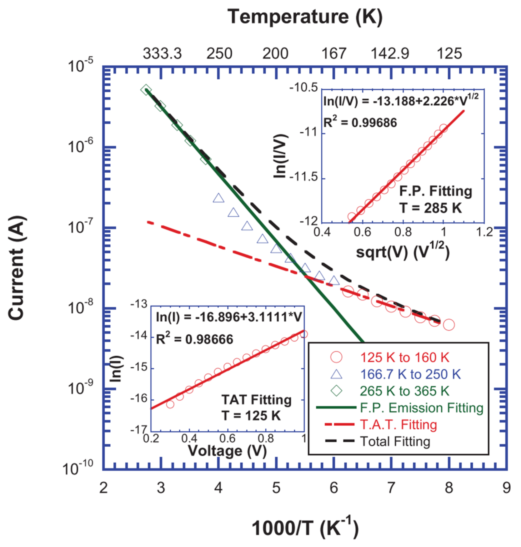
3.3. Poole-Frenkel (P-F) Emission

The P-F emission happens when trapped electrons get excited into the conduction band of the oxide. The electric field decreases the Coulombic potential barrier of the electrons and subsequently increases its probability for being thermally excited out from the traps [70]. The exponential portion of P-F expression is very similar to Schottky emission, except the junction barrier height (ΦB) is replaced with the depth of traps’ potential well (ΦT) and the barrier lowering effect in P-F is double of Schottky emission due to immobility of positive charge [78,79]. The schematic energy band diagram of P-F emission is depicted in Figure 7.
The current density JPF can be expressed as Equation (5) [71]:
J P F = q μ N C E exp [ q ( ϕ T q E / πε ) k T ]
where µ is the electronic drift mobility, NC is the density of states in conduction band, E is the applied electric field, ΦT is the depth of traps potential well, k is Boltzmann’s constant and T is the absolute temperature.
Figure 7. Schematic energy band diagram of Poole-Frenkel emission in MIM structures.
Electronics 04 00586 g007

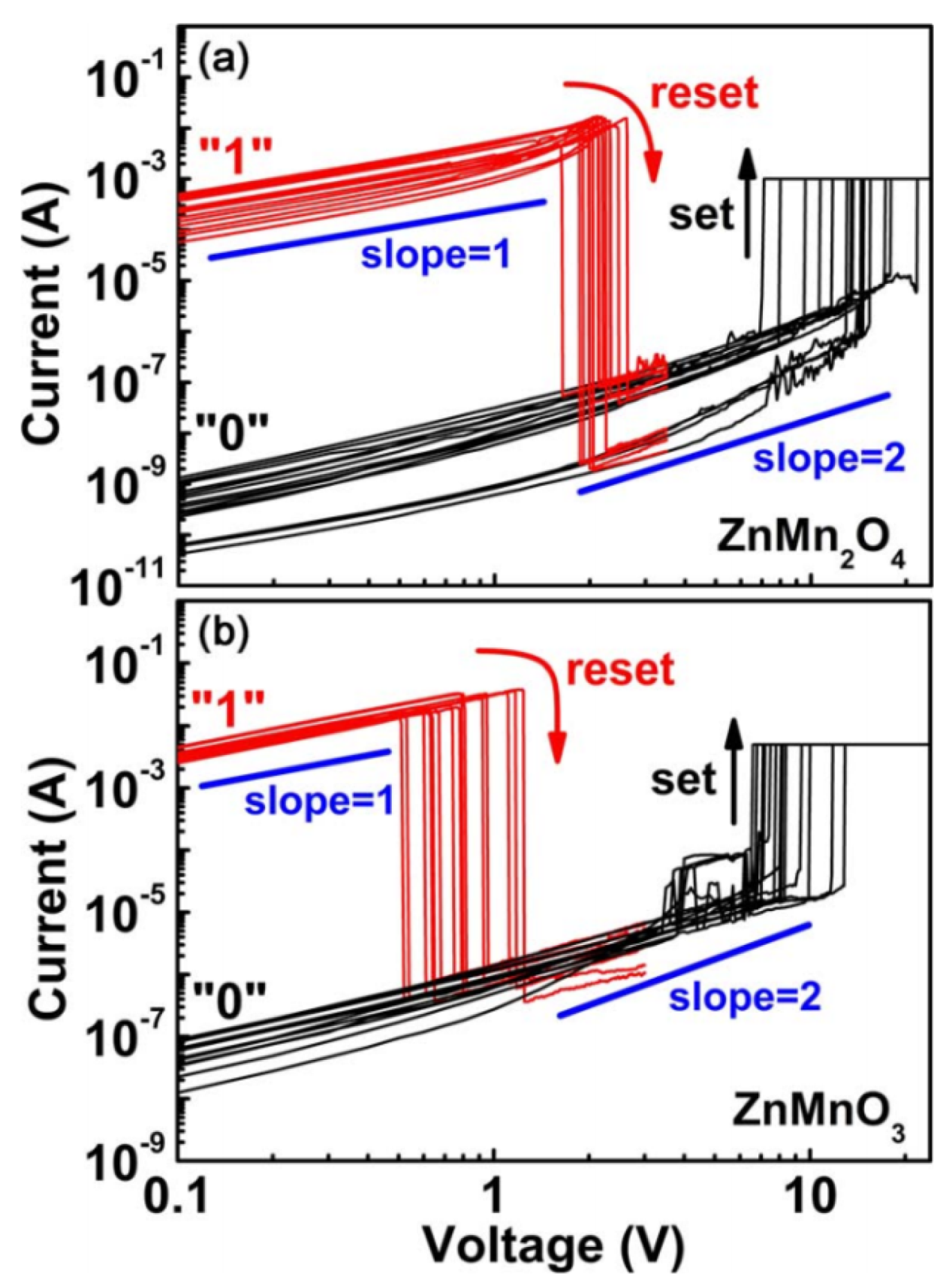
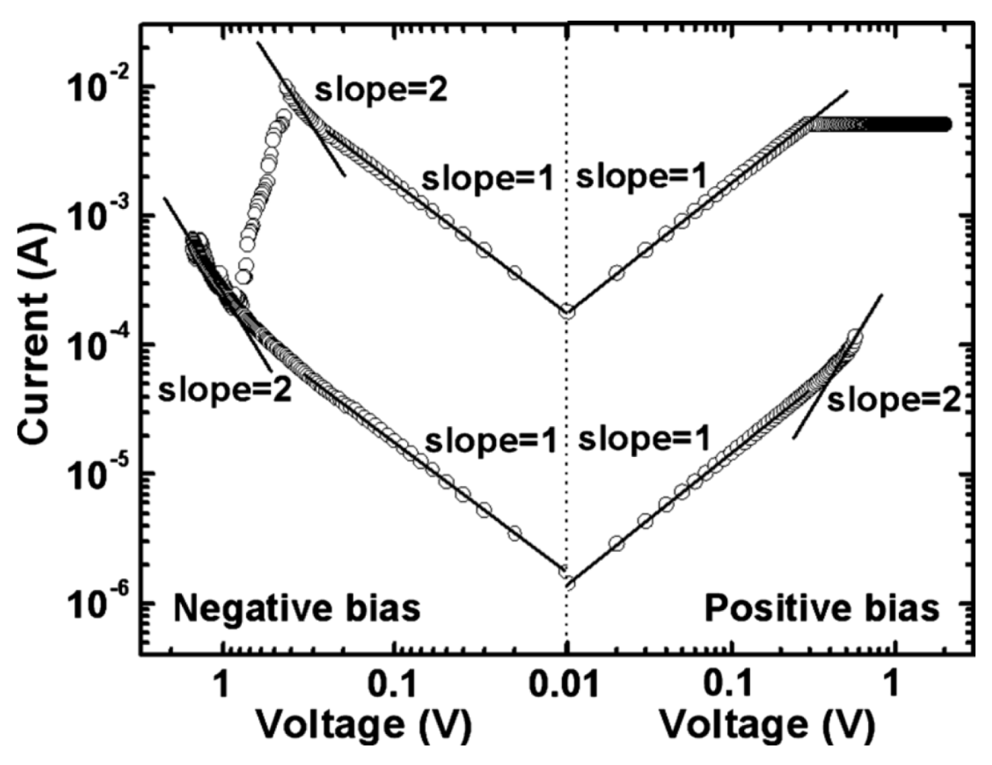
3.4. Space-Charge-Limited-Conduction (SCLC)

A trap-controlled SCLC is constituted of three portions: The Ohmic region (I V), the Child’s square law region (I V2) and the steep increase in the high field region [80]. This mechanism could be easily identified whenever Ohmic conduction is observed at low field, followed by power-law dependence (I V2) of the current density is observed in high field [80,81,82]. In low field regime, the conduction mechanism is dominated by the thermally generated free electrons in the oxide film. When the field exceeds the square-law onset voltage, the density of electrode-injected electrons gradually exceeds the equilibrium concentration and dominating the conduction [43]. The I V2 region is known as trap-unfilled SCLC region, while the third region is often referred as trap-filled SCLC region. Hence, the probability of SCLC conduction is usually higher if the electrode’s contact is highly carrier injective [52]. According to the SCLC theory [83], for the simple case of a single discrete trapping level, the current density at high field is given by Equation (6) [84]:
J S C L C = 9 8  ε i μθ V 2 d 3
where εi is the permittivity of the oxide, µ is the mobility, θ is the ratio of free and shallow trapped charge, and d is thickness of the oxide.

3.5. Ionic Conduction

Movement of ions under influence of an applied electric field attributes to ionic conduction which is similar to a diffusion process [78]. The ionic current density is proportional to ion drift velocity and the general expression is given by Equation (7) [85,86]:
J i o n i c v r   ·   exp ( G k T ) { e x p ( 1 2 r e k T E ) e x p ( 1 2 r e k T E ) }
where v is the Debye frequency, r is the jump distance, ∆G is the free activation enthalpy and E is the electric field. In the case of low electric fields (EkT/re), the current density is linearly related to electric field and can be approximated to Equation (8):
J i o n i c ( l o w E ) ( v r 2 e k T ) · E   ·   exp ( G k T )
For high field (EkT/re), the current density is exponentially related to electric field as shown in Equation (9):
J i o n i c ( h i g h E ) v r   ·   exp ( G k T ) ·   e x p ( 1 2 r e k T E )

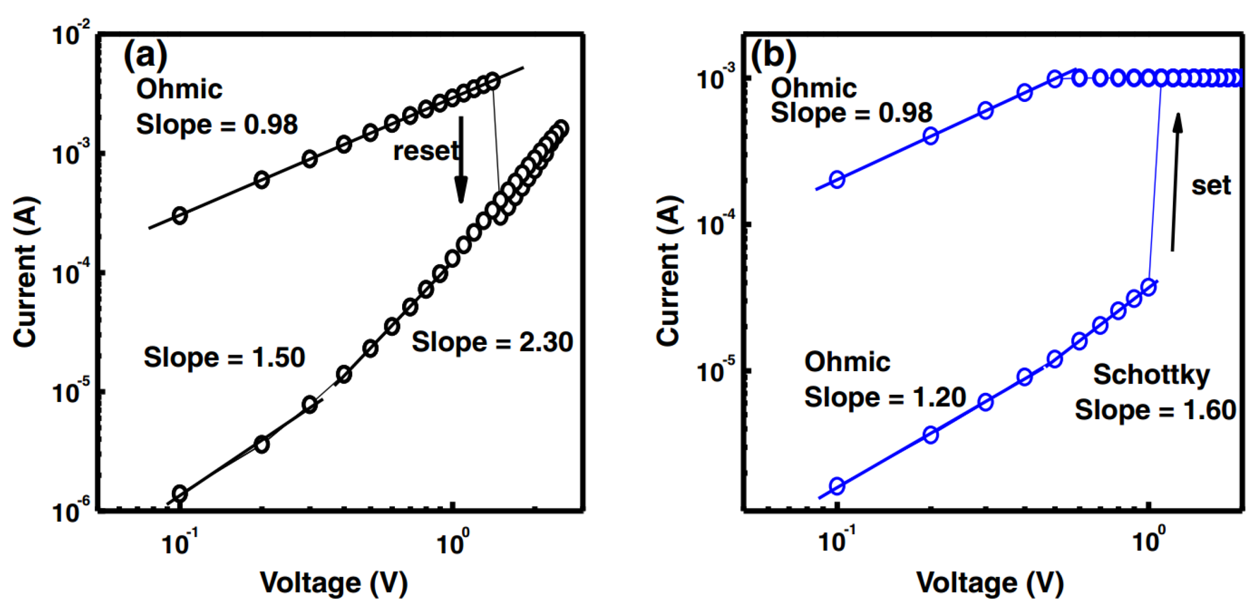
3.6. Ohmic Conduction

There are a small number of mobile electrons that get generated due to thermal excitation, even though the energy band gap of the oxide is by definition large. These electrons attribute to the Ohmic conduction in which the current density is proportional to the electric field and is relatively obvious in HRS. Equation (10) represents the current density of the Ohmic conduction.
J o h m i c = σ E = q μ N C E exp [ ( E C E F ) k T ]
where σ is electrical conductivity, µ is the electron mobility, Nc is the effective density of states of the conduction band, EC is the conduction band and EF is the Fermi energy level.

3.7. Nearest Neighbor Hopping (NNH)

NNH also known as fixed range hopping (FRH). Oxide layer often contains defects known as traps. Electrons that trapped in one trap site can hop into other nearest trap sites through tunneling effect. The current density due to this mechanism can be represented by Equation (11) [87].
J N N H = σ 0 exp ( T 0 T ) · E
where σ0 is the electrical conductivity at temperature of T0.

3.8. Mott Variable Range Hopping (VRH)

In addition to NNH, Mott VRH is another widely studied hopping conduction mechanism. Mott VRH describes the electron hopping behavior in strongly disordered systems with localized charge-carrier states [87], and has been suggested to be the main conduction mechanism in the semiconducting CFs [22]. In contrast with NNH, where the trap electrons are expected to hop into the nearest neighboring trap, the electrons under the VRH scheme may hop into traps that are further away but have lower trap energy. Figure 8 illustrates the energy band diagram of NNH and VRH mechanism.
Figure 8. Schematic energy band diagram of Nearest Neighbor Hopping (NNH) and Variable-range Hopping (VRH) model in an MIM structure.
Electronics 04 00586 g008
In term of the I-V characteristic, the Mott VRH current is similar to Ohmic conduction where it is proportional to applied electric field. However, the conductance (σ) of Mott VRH demonstrates temperature dependency (ln(σ) ∝ T−1/4) as shown in Equation (12) [87]:
J V R H = σ 0 exp ( T 0 T ) 1 4 · E
where σ0 is the electrical conductivity at temperature of T0.

3.9. Trap-Assisted Tunneling (TAT)

TAT is attributed to the tunneling currents assisted by the defects in the dielectric [88,89]. In contrasts to single step tunneling process like F-N tunneling or direct tunneling, the traps (e.g., oxygen vacancies) in oxide layer assist the electrons to tunnel from cathode to anode through a 2-steps process [90]. The electrons are first captured from the cathode into the traps and subsequently emitted to anode. For inelastic TAT, the electron will relax to the trap’s energy level by emitting one or more phonons with the energy ℏω [91]. The generalized expression of the TAT current is quite similar to the F-N tunneling except for the E2 factor, and can be written as in Equation (13) [92]:
J T A T = A  exp ( 8 π 2 q m * 3 h E ϕ T 3 / 2 )
where A is a constant and ΦT is the energy of the electron traps with respect to the conduction band edge of the oxide.

3.10. Summary

Table 1 summarizes the basic conduction expression in oxide layer and highlights the electric field and temperature dependency.
Table 1. Expression and field/temperature dependency of typical conduction mechanism in dielectric film.
Conduction MechanismCurrent Density ExpressionElectric Field and Temperature Dependency b
Schottky Emission J S E = 4 π q m * ( k T ) 2 h 3 exp [ q ( ϕ B q E / 4 πε ) k T ] J S E T 2 exp ( A E T B )
Fowler-Nordheim (F-N) Tunneling J F N = q 2 8 π h ϕ B E 2 exp ( 8 π 2 q m * 3 h E ϕ B 3 / 2 ) J F N E 2 exp ( A E )
Direct Tunneling J D T exp { 8 π 2 q 3 h ( m * ϕ B ) 1 / 2 κ · t o x , e q } J D T exp ( A · κ t o x , e q )
Poole-Frenkel (P-F) Emission J P F = q μ N C E exp [ q ( ϕ T q E / πε ) k T ] J P F E · exp ( A E T B )
Space-charge-limited Conduction (SCLC) a J S C L C = 9 8  ε i μθ V 2 d 3 J S C L C E 2
Ionic Conduction J i o n i c E T exp { G k T } J i o n i c E T exp ( A T )
Ohmic Conduction J o h m i c = σ E = q μ N C E exp [ ( E C E F ) k T ] J o h m i c E · exp ( A T )
Nearest Neighbor Hopping (NNH) J N N H = σ 0 exp ( T 0 T ) · E J V R H E · exp ( A T )
Variable-range Hopping (VRH) J V R H = σ 0 exp ( T 0 T ) 1 4 · E J V R H E · exp ( A T ) 1 4
Trap-assisted Tunneling (TAT) J T A T = A  exp ( 8 π 2 q m * 3 h E ϕ T 3 / 2 ) J T A T exp ( A E )
a High field only, low field follows Ohm’s Law; b A & B are constants.

4. Conduction Mechanism of Published Resistive Switching Memories

In this section, we will review selected published works where the dominant conduction mechanism are explicitly studied and reported. These works are categorized and listed in Table 2, Table 3, Table 4, Table 5 and Table 6 based on corresponding dominant conduction mechanism. Please note that the works reported are by far not exhaustive. The tables here only cover a subset of the huge collection of published resistive switching devices. Others transport models that requires iterative or numerical calculation, such as Menzel model [93], domain-based model [94,95], drift-diffusion model [96], ion-transport-recombination model [97,98,99] and hourglass model [100,101] are deliberately omitted in this article.

4.1. Poole-Frenkel (P-F) Emission

Devices with conduction dominated by P-F emission should exhibits linear fitting when the I-V characteristic is plotted on ln(J/E) vs. (E1/2/T) graph. This conduction mechanism has been widely observed in HRS of several resistive switching devices that based on materials such as SnOx [24], ZnO [25,26], AlOx [27], CeOx [28], WOx [29], LaHoO3 [30] and etc. as listed in Table 2.
Table 2. Published works with P-F emission observed.
ReferenceElectrode/Material(s)/ElectrodeConduction Mechanism
LRSHRS
Low VHigh V
Nagashima et al., 2009 [24]{Pt,Au,Ti}/SnO2/PtSEP-F
Lee et al., 2009 [25]Au/ZnO/SSOhmicOhmicP-F
Chan et al., 2012 [26]Al/ZnO/SiSCLCP-F
Kim et al., 2014 [27]Al/N-AlOx/AlP-FP-F
Sharma et al., 2014 [102]Pt/SmGdO3/PtOhmicP-F
Ismail et al., 2015 [28]TaN/CeOx/PtOhmicP-F
Hong et al., 2015 [29]Ti/WOx/PtOhmicOhmicP-F
Sharma et al., 2015 [30]Pt/LaHoO3/PtOhmicP-F
Mahapatra et al., 2015 [31]Au/HfOx/TiOx/HfOx/PtOhmicP-F
Guo et al., 2015 [32]Pt/Ga2O3−x/PtOhmicOhmicP-F
Figure 9a,b show the I-V characteristic of unipolar SnO2-based device with three different materials as top electrodes (Pt, Au and Ti) as reported by Nagashima et al. [24]. As shown in Figure 9d, the I-V curve in HRS is well fitted to P-F emission model (ln(J/E) ∝ E1/2). This indicates that the conduction mechanism of this 40 nm thick crystalline SnO2 is dominated by the electrons that hopping from the trap states into conduction band under high electric field.
Figure 9. J-E plots of SnO2 in (a) LRS and (b) HRS when using Pt, Au and Ti as top electrodes. (c,d) show the comparisons with Schottky emission model and Poole-Frenkel emission model, respectively. Reprinted with permission from [24]. Copyright © 2009, American Institute of Physics.
Electronics 04 00586 g009
As reported by Lee et al. [25], comparable behavior is observed in the flexible ZnO-based device with Au and stainless steel as electrodes. In LRS, the J vs. E plot shows strong linear relationship with slope close to one, indicating that conduction mechanism in LRS is governed by Ohmic conduction. For HRS regime, it is observed that the conduction mechanism continue to be governed by Ohmic conduction at low field, while the nonlinear effect is getting dominance at high voltages (E > 0.1 MV/cm). This non-linear region has good agreement with the P-F emission model (ln(J/E) E1/2). In a separate work, Chen et al. [26] also observed P-F emission on self-rectifying memory device based on same material (ZnO). The HRS current of the device, which using Al and Si as electrode, can be fit to the P-F emission with a slope of ~1.56.
Kim et al. [27] obtained excellent fitting for both P-F and Schottky emission in the nitrogen-doped forming-free AlOx device, because both mechanisms have similar linear dependency between current and the square root of voltage when measured under fixed temperature. Although Schottky emission has strong temperature dependency (J T2) and could be used to differentiate it from P-F emission, however Kim et al. has to omit this option as infeasibility to increase the temperature of the test structure by few orders of magnitude. In turn, another approach was proposed, where the trap energy barriers (ΦT) of P-F emission model and Schottky barrier (ΦB) of Schottky emission model are extracted from respective slope in the fitted curve and compared with the expected values. It was found that the extracted barrier (ΦB) from Schottky emission plot is unreasonably low and the authors conclude that P-F emission is more appropriate description for the conduction mechanism in N-doped AlOx device.
Sharma et al. reported similar conduction mechanism in rare-earth based oxide memories, such as Pt/SmGdO3/Pt [102] and Pt/LaHoO3/Pt [30]. In both cases, a linear relationship between ln(J/E) vs. E1/2 confirmed the domination of Poole-Frenkel emission in OFF state. In the SmGdO3 sample, Ohmic conduction was observed at low voltage regime (<0.6 V) of the ON state. Whereas minor deviation from initial linearity was observed in high voltage regime (>0.6 V). The deviation in resistance is probably due to Joule-heating.
Similarly, the I-V characteristic of Cerium oxide-based memory reported by Ismail et al. [28] resembles the findings in [27], which have good linear fit to both P-F emission and Schottky emission. Anyhow, the observed current does not demonstrate strong correlation in the plot of ln(I/T2) against 1/T, which is expected in Schottky emission. Therefore, the authors suggest that the conduction in this 15 nm thick CeOx device is dominated by P-F emission.
Overall, linearity relation in the ln(J/E) vs. E1/2 plot is a well-accepted approach in identifying the P-F emission. Additional checks such as temperature dependency (ln(J/T2) ∝ 1/T) and I-V symmetric check are usually employed to distinguish P-F emission from the electrode-limited Schottky emission.

4.2. Schottky Emission

As tabulated in the Table 1, current density attributed to Schottky emission has dependency on both temperature (T) and electric field (E). Hence, the existence of Schottky emission can be ascertained by fitting to two functions, which are: (i) ln(J/T2) 1/T under fixed electric field; and (ii) ln(J) ∝ E1/2 under fixed temperature. There are numerous published resistive switching devices that suggested Schottky emission as the dominant conduction mechanism, such as [33,34,35,36,37,38,39,40,41,42], etc. The combination of electrodes and materials of these works is listed in Table 3.
Table 3. Published works with Schottky emission observed.
ReferenceElectrode/Material(s)/ElectrodeConduction Mechanism
LRSHRS
Low VHigh V
Cao et al., 2009 [33]Pt/TiO2/PtOhmicOhmic
Huang et al., 2010 [34]Ti/TiO2/PtSESE
Lee et al., 2012 [35]TiN/Ti/TiOx/HfOx/TiNSESE
Zhu et al. 2012 [36]Al/anodic AlOx/AlOhmicBoth P-F and SE
Syu et al., 2013 [37]Ti/HfO/TiNOhmicSE
Kuo et al., 2014 [38]Al/VOx/CuOhmicSE
Zhang et al., 2014 [39]ITO/Gd:SiO2/TiNSESE
Zhong et al., 2014 [40]Cu/SiC/AuOhmicSEP-F
Mondal et al., 2014 [42]Ni/Sm2O3/ITOOhmicSE
Hsieh et al., 2015 [41]Ni/ZnO/HfO2/NiOhmicSE
Cao et al. [33] compared I-V characteristic of the unipolar switching Pt/TiO2/Pt device with several non-linear conduction mechanisms including P-F emission, SCLC and Schottky emission, and found that the experimental data fit perfectly to Schottky emission model with slope of 3.553 in the double-logarithmic plot of I-V.
Huang et al. [34] observed comparable conduction mechanism in the resistive switching Ti/TiO2/Pt diode which prepared using a simple evaporation process. The asymmetry of J-V curves as shown in Figure 10 is the result of unequal Schottky barriers at the Ti/TiO2 (0.13 eV) and the TiO2/Pt (0.73 eV) interfaces. Since Schottky emission is the electrode-limited conduction mechanism, the I-V characteristic of devices with heterogeneous electrode material tends to demonstrate asymmetric property, which can be used to differentiate Schottky emission from other bulk-limited conduction mechanism such as P-F emission.
Figure 10. J-V characteristics of a typical Pt/TiO2/Ti MIM diode. The thickness of TiO2 is 8 nm. Insets show the band structures of the MIM under different biases and the Schottky emission fitting of ln(J) vs. E1/2 from −0.4 V to −4 V, respectively. Reprinted with permission from [34]. Copyright © 2010, American Institute of Physics.
Electronics 04 00586 g010
Similar asymmetrical property of I-V relation is also witnessed in Lee et al.’s experiment on TiN/Ti/TiOx/TiN structure and the double-layered TiN/Ti/TiOx/HfOx/TiN structure [35]. It is clearly seen that the single layer structure demonstrates stronger symmetrical property in I-V characteristic compared to double layered structure. In the single layer structure, Schottky barrier at Ti/TiOx and TiOx/TiN interface are 0.17 eV and 0.3 eV respectively. Meanwhile, the Schottky barrier of additional HfOx/TiN interface in the double-layered structure is relatively higher at 2.36 eV.
Zhu et al. [36] observed that the anodic-AlOx device with homogenous Al electrode is fit to both P-F and Schottky emission expression. Since symmetrical check on I-V relation is not possible due to homogenous electrodes, Zhu et al. resorted to compare the activation energies (Ea) extracted from the respective Arrhenius plots, but found that the extracted values are close (0.41–0.43 eV) and indecisive. Thus, this is a rare case where no clear evidence on whether P-F or Schottky emission is governing the conduction.
Sun Kuo et al. employed Schottky emission to explain the increasing HRS resistance during cycling operation on the Al/VOx/Cu [38]. Noted that Al electrode has lower work function (4.28 eV) thus can form a Schottky barrier with p-type VOx that has higher work function of 4.7 eV. A good linear relation of ln(J) and V1/2, indicating the Schottky emission is the dominant conduction mechanism in HRS. For LRS, the I-V fitting and conductive atomic force microscopy (CAFM) image suggest that Ohmic conduction is the dominant current.
Hsieh et al. [41] compared the I-V characteristic of double-layered ZnO/HfO2 memory with the P-F and Schottky emission fittings. The plots are found to have better fit with Schottky current model.
By and large, fitting of ln(J)-E1/2 function with fixed temperature is broadly adopted in classifying Schottky emission. The additional temperature dependency check (ln(J/T2)   1/T) is sometime omitted due to infeasibility in adjusting the temperature. In some cases where the top and bottom electrodes have relatively big difference in work function, asymmetry I-V characteristic could be observed.

4.3. Space Charge Limited Conduction (SCLC)

SCLC is another commonly observed conduction mechanism in published resistive memories. Signature of SCLC is relatively observant with two regions of distinct slope when the I-V characteristic is plotted in double-logarithmic scale. The I-V relation follows Ohmic law (I V) in low field regime, and Child’s Law (I V2) in high field regime. In HRS, the third region could be observed in which the current will increase rapidly due to the formation of CF. Table 4 lists some published works in which the SCLC characteristic is observed.
Yu et al. [43] reported that both LRS and HRS of the Al/TiOx/Al device is governed by the SCLC conduction mechanism. The Ohmic conduction behavior (IV) is observed in low voltage region where V < 0.1 V, and followed by a quadratic term (IV2) as defined by Child’s Law in V > 0.1 V.
The SCLC mechanism is also identified to be the dominant conduction mechanism in Au/Cr/Zr+-implanted-ZrO2/Si device as reported by Liu et al. [44]. The fitting of each SCLC regions for both positive and negative voltage range are clearly shown SCLC behavior. By leveraging the expression for trap-controlled SCLC as listed in Equation (5), the role of implanted Zr+ in resistive switching phenomenon is explained in the work.
Table 4. Published works in which space charge limited conduction (SCLC) is observed.
ReferenceElectrode/Material(s)/ElectrodeConduction Mechanism
LRSHRS
Yu et al., 2008 [43]Al/TiOx/AlSCLCSCLC
Liu et al., 2008 [44]Au/Cr/Zr+ implanted ZrO2/SiSCLC and OhmicSCLC
Peng et al., 2009 [45]Au/ZnMn2O4/Pt Au/ZnMnO3/PtOhmicSCLC
Wang et al., 2010 [46]Ti/CuxO/PtSCLCSCLC
Kim et al., 2010 [47]Al/TiOx/TiO2/AlSCLCSCLC
Lee et al., 2009 [48]TiN/AlCu/HfOx/TiNSCLCSCLC
Lee et al., 2010 [49]TiN/Ti/HfOx/TiNSCLCSCLC
Chen et al., 2010 [50]Cu/AlN/PtOhmicSCLC
Mondel et al., 2014 [42]Ni/Lu2O3/ITOOhmicSCLC
Fu et al., 2014 [51]Ag/La0.5Sr0.5CoO3/PtSCLCSCLC
Ismail et al., 2014 [52]Zr/CeOx/PtOhmicSCLC
Zeng et al., 2014 [53]Pt/ZrO2/TiO2/PtOhmicSCLC
Kim et al. [47] reported the observation of the SCLC conduction in Al/TiOx/TiO2/Al device. Three regions with distinct slope differences are noted in the double-logarithm I-V plots. The author also includes the P-F emission and thermionic (Schottky) emission curve in same plot for comparison.
Figure 11. (a) Relation of log(I) vs. log(V) for the positive applied voltage range from 0 V to 2 V; (b) Relation of log(I) vs. log(V) for the negative applied voltage range form −2 V to 0 V. Reprinted with permission from [51]. Copyright © 2014, American Institute of Physics.
Electronics 04 00586 g011
Fu et al. [51] exhibited that the conduction mechanism in La0.5Sr0.5CoO3(LSCO)-based device is also agree with SCLC description. As shown in Figure 11, both positive and negative voltage range demonstrates the clear signature of SCLC mechanism, which has three regions with noticeable slope difference. The conduction characteristics of this perovskites-based device can be explained by the injected hole carrier and is depend on Ag/LSCO and Pt/LSCO interfaces traps that are exponentially distributed in energy.
Among the reviewed literatures, whenever SCLC behavior is observed in HRS, the same mechanism tends to dominate in LRS as well. However, there are few exceptions, such as [45,46,50,52,53] where only Ohmic conduction is observed in LRS.
In Cu/AlN/Pt device developed by Chen et al. [50], the square-law onset voltage observed in HRS is about 0.125 V. However, the current in LRS is already concealed at compliance current (Icomp) around 0.11 V.
In [45], both the ZnMn2O4 and ZnMnO3 samples have the square-law onset voltage around 2 V in HRS. The Vreset of ZnMnO3 sample is lower than this square-law onset voltage and the current shows a strong linearity relation with the voltage over the whole LRS range. In contrast, some minor non-linearity is observed during the LRS to HRS transition in the ZnMn2O4 sample, which has slightly higher Vreset as depicted in Figure 12. Therefore, it is believed that the CF is ruptured and reset to HRS before the ZnMn2O4 device moved into trap-unfilled SCLC region (I-V2).
Figure 12. Typical resistive switching characteristics of (a) Au/ZnMn2O4/Pt; and (b) Au/ZnMnO3/Pt devices in log-log scale. Adapted from [103].
Electronics 04 00586 g012
Wang et al. [46] reported that the SCLC is the dominant conduction mechanism in HRS and negative-based LRS of the Ti/CuxO/Pt device. However, there is no I-V2 region observed in positive-biased LRS as shown in Figure 13, which could be capped by the current compliance imposed on the device.
Figure 13. I-V characteristics of both the positive and negative bias regions of the Ti/CuxO/Pt device plotted in a double-logarithmic scale. Both ON-state and OFF-state are included in this plot. Reprinted with permission from [46]. Copyright © 2010, American Institute of Physics.
Electronics 04 00586 g013
Similarly, for the Zr/CeOx/Pt memory device [52], the Ohmic conduction in LRS can be explained by the current compliance limit in negative voltage region and low Vreset in positive voltage region as shown in Figure 14.
Figure 14. I-V curves for Zr/CeOx/Pt memory device are displayed in double-logarithmic scale. The linear fitting results in both ON state and OFF state: (a) positive-voltage region; and (b) negative-voltage region. Adapted from [52].
Electronics 04 00586 g014
Generally, observation of three apparent regions where (i) IV, (ii) IV2 and (iii) steep increase of I, signifies the dominant of SCLC mechanism. To summarize, SCLC conduction has been observed in wide range of materials and it is commonly accepted that the defect-related traps, e.g., oxygen vacancies, are contributing to the SCLC conduction.

4.4. Trap-Assisted Tunneling (TAT)

I-V characteristic of TAT conduction could be fit linearly in the plots of ln(J) versus 1/E. Besides this, microscopic models such as multi-phonon TAT (MTAT) model are often used. The TAT conduction modeling is found to be consistent with some experimental data based on HfOx [54,55,56], TaOx [57] and SiOx [58,59] as depicted in Table 5.
Table 5. Published works with trap-assisted tunneling (TAT) Observed.
ReferenceElectrode/Material(s)/ElectrodeConduction Mechanism
LRSHRS
Bersuker et al., 2011 [54]TiN/HfO2/TiNOhmicTAT
Yu et al., 2011 [55]TiN/HfOx/PtTATTAT
Long et al., 2012 [56]Ru/HfO2/TiOx/RuOhmicTAT(Low T), P-F(High T)
Jeon et al., 2014 [57]Pt/TaOx/TaON/PtOhmicP-F and TAT
Mehonic et al., 2012 [58]ITO/SiOx/p-type Si/CrTATF-N and TAT
Bersuker et al. [54] analyzed the conduction mechanism in TiN/HfO2/TiN device by using the statistical multi-phonon trap-assisted tunneling (MTAT) model. The model is a quantitative physical model that takes into account of the lattice relaxation due to electron-phonon coupling as well as the microscopic structural changes associated with the concentration of the defects [104,105]. The simulated result has good agreement with experimental data when voltage >0.8 V and temperature between 300 K and 400 K.
Yu et al. [55] used process of elimination to pinpoint the dominant conduction mechanism in the TiN/HfOx/Pt device which fabricated using atomic layer deposition (ALD) method [106]. The P-F emission option was dismissed due to nonlinear curve on ln(I/V) vs. V1/2 plot as well as unrealistic extracted trap energy (ET) and dielectric constant (εr). Schottky emission and F-N tunneling were also ruled out due to weak dependency on temperature and electric field respectively. Direct tunneling was also excluded as it should be negligible in the 10 nm thick HfOx film. Along these lines, the remaining probable conduction mechanism is TAT. The hypothesis was then evaluated by using current modeling that takes into account of the electron transition rate and transmission probability that is calculated with Wigner-Kramers-Brillouin (WKB) approximation. Several follow-up models from the same group, i.e., stochastic model [107] and Kinetic Monte Carlo (KMC) model [108], further corroborated the TAT as dominant conduction mechanism.
Mehonic et al. [58] reported a comparable conduction mechanism in 35 nm thick SiO2-based device but utilizing a much compact approach which the current density is fitted to an expression with respect to electric field and trap’s energy barrier (ΦT) [92] as shown in Equation 10. The negative linear relation in the ln(J) vs. 1/E plots clearly exemplifies the TAT conduction in both LRS and HRS. The extracted trap energy barrier (ΦT) of HRS and LRS are 1.06 eV and 0.41–0.63 eV respectively [59].
Long et al. [56] affirmed the role of Ohmic conduction during LRS in 6 nm thick HfO2-based device. However, the conduction in HRS is found to be governed by combination of both P-F emission and TAT process. As shown in Figure 15, the experimental data is close to TAT fitting on 125–160 K, while P-F emission seen dominating at 265–365 K.
Similarly, TAT conduction is observed in addition to P-F emission in single layer Pt/TaOx/Pt device as reported by Jeon et al. [57]. However, the energy of electron traps ΦT that extracted from plain P-F emission fitting is not consistent with value observed using spectroscopic ellipsometry (SE). Thus, the most appropriate conduction mechanism in this Pt/TaOx/Pt device is probably TAT.
When comparing to other conduction mechanisms, the usage of expression fitting is not as popular in identifying TAT. Most researchers relate TAT conduction via process of elimination and microscopic modeling. Generally, it is accepted that oxygen vacancy defects near the cathode is playing a critical role in conduction mechanism [55,109]. Hence, TAT has broadly employed to explain the electron transport mechanism in oxide thin film with high defect density.
Figure 15. HRS fitting of HfO2 based device for F-P emission between 190 K and 365 K and TAT fitting between 80 K and 97.6 K. Reprinted with permission from [56]. Copyright © 2012, American Institute of Physics.
Electronics 04 00586 g015

4.5. Hopping Conduction

Nearest Neighbor Hopping (NNH) and Mott Variable-range Hopping (VRH) are the hopping conductions, which commonly observed in resistive switching memories. The devices dominated by these hopping conductions exhibit temperature dependency, i.e., ln(σ) ∝ T−1 for NNH and ln(σ) ∝ T−1/4 for VRH. Table 6 lists some of the published works which hopping conduction is reported to be the dominant conduction mechanism.
Table 6. Published works with TAT observed.
ReferenceElectrode/Material(s)/ElectrodeConduction Mechanism
LRSHRS
Ho et al., 2007 [60]TiN/WOx/WOhmicVRH
Wei et al., 2011 [61]Ir/Ta2O5−σ/TaOx/TaNFRH(high T), VRH(low T)
Phan et al., 2012 [62]Pt/Cr-SrTiO3/La0.5Sr0.5CoO3VRH(V>0), SCLC(V
Sekar et al., 2014 [63]TiN/TaOx/HfO2/TiNVRHNNH
Zhang et al., 2014 [64]Pt/TaOy/Ta2O5−x/PtNNH(high T), VRH(low T)
Fang et al., 2015 [65]Pt/HfOx/TiNNNH(high T), VRH(low T)
Ho et al. [60] reported that two different characteristic of I-V behaviors are observed in the WOx-based device, i.e., linear in LRS and non-linear in HRS. The LRS conduction is believed to be governed by metallic conduction because of the Ohmic I-V characteristic and finite residual resistance at low temperature. In HRS, the I-V curve is well fitted to a straight line in ln(J) ∝ T−1/4 plot, suggesting that the current is primarily due to Mott VRH. A good hyperbolic-sine fitting of the I-V curve further agreed the role of Mott VRH in HRS current conduction.
Both Mott VRH and Fixed-range Hopping (FRH) are observed in the Ir/Ta2O5−σ/TaOx/TaN device as reported in [61]. The I-V plot fitted the Mott VRH criteria in temperature lower than 200 K, and FRH criteria in the higher temperature. From the plots of ln(σ) versus 1/T, an obvious slope-switching points is observed around 200 K, implying the dominating current mechanism is switching toward Mott VRH from FRH when the temperature decreases beyond 200 K.
Phan et al. [62] verified that I-V characteristic of Cr-doped SrTiO3 thin firm is matching the Mott VRH model in positive biased regime and trap-controlled SCLC model in negative biased regime. Within the Mott VRH dominating region, conductance shows temperature dependency (ln(I) ∝ T−1/4) when bias voltage is below +1 V and electrical field dependency (ln(I) ∝ E−1/4) when bias voltage is above +1 V.
Similar to [61], Zhang et al. [64] also observed temperature dependency of the hopping conduction in TaOy/Ta2O5−x device. Two distinct slopes can be seen in the plot of ln(σ) against 1000/T. There is good fit to NNH expression (slope ~1) at temperature above 50 K, and VRH expression (slope ~1/4) at temperature below 50 K.
Fang et al. [65] reported that the resistance in both LRS and HRS of Pt/HfOx/TiN device increases linearly with respect to exp(1/kT), and tends to saturate at temperature below 77 K. The slope of this fitted curve is also being used to extract device parameters such as hopping barrier Ea based on the hopping conduction expression as in Equation (14) [71,110]:
J h o p = q a n v  exp ( q a E k T E a k T )
where a is the mean spacing between trap sites or the hopping distance, n is the electron concentration in the conduction band of the dielectric, v is the frequency of thermal vibration of electrons at trap sites and Ea is the barrier height between two traps. This indicates that the slope of ln(J) versus 1/T plots can be related to the difference of field-driven barrier lowering (qaE) and hopping barrier between traps (Ea).
Generally, resistive switching materials tend to have high density of traps, hence it allows trap electrons to hop from one to other traps. The conductance due to these hopping electrons demonstrates temperature dependency, i.e., ln(σ) ∝ T−1/4 for Mott VRH and ln(σ) ∝ T−1 for NNH or FRH.

5. Conclusions

We described and analyzed some commonly observed conduction mechanisms of resistive switching memories, namely, Poole-Frenkel (P-F) conduction, space charge limited conduction (SCLC), Schottky emission, trap-assisted tunneling (TAT) and hopping conduction. We found that the resistive switching memories do not demonstrate the same I-V characteristic even when built with the same materials. This could be due to other attributes such as electrode material, oxide properties (thickness, bandgap, trap energy level), fabrication process (annealing temperature and ambient), operating temperature and interfacial barrier height between metal and oxide. Generally, fitting to expression of typical conduction mechanisms is the most popular approach to identify the dominant conduction contributor. In some cases, additional analysis is carried out on the symmetrical property of the I-V characteristic and extracted physic parameters. However, the drawback of these techniques is that they rely on the assumption that electron transport is only governed by a single mechanism. This ignores the fact that multiple mechanisms can collectively contribute to the conduction depending on the temperature, applied electric field and voltage polarity. Thus, a generalized conduction modeling which incorporating concurrent contribution from major conduction mechanisms should be leveraged to enable accurate I-V characteristic modeling over various materials and operating scenarios.

Acknowledgments

The authors would like to thank the Research Management Center (RMC) of Universiti Teknologi Malaysia (UTM) for providing excellent research environment in which to complete this work.

Conflicts of Interest

The authors declare no competing financial interest. We have also diligently secured copyrights for already published materials used in this review paper.

References

  1. Pan, F.; Gao, S.; Chen, C.; Song, C.; Zeng, F. Recent progress in resistive random access memories: Materials, switching mechanisms, and performance. Mater. Sci. Eng. R. Rep. 2014, 83, 1–59. [Google Scholar] [CrossRef]
  2. Wong, H.S.P.; Salahuddin, S. Memory leads the way to better computing. Nat. Nanotechnol. 2015, 10, 191–194. [Google Scholar] [CrossRef] [PubMed]
  3. Choi, B.J.; Torrezan, A.C.; Norris, K.J.; Miao, F.; Strachan, J.P.; Zhang, M.X.; Ohlberg, D.A.A.; Kobayashi, N.P.; Yang, J.J.; Williams, R.S. Electrical Performance and Scalability of Pt Dispersed SiO2 Nanometallic Resistance Switch. Nano Lett. 2013, 13, 3213–3217. [Google Scholar] [CrossRef] [PubMed]
  4. Lee, M.J.; Lee, C.B.; Lee, D.; Lee, S.R.; Chang, M.; Hur, J.H.; Kim, Y.B.; Kim, C.J.; Seo, D.H.; Seo, S.; et al. A fast, high-endurance and scalable non-volatile memory device made from asymmetric Ta2O5−x/TaO2−x bilayer structures. Nat. Mater. 2011, 10, 625–630. [Google Scholar] [CrossRef] [PubMed]
  5. Wei, Z.; Kanzawa, Y.; Arita, K.; Katoh, Y.; Kawai, K.; Muraoka, S.; Mitani, S.; Fujii, S.; Katayama, K.; Iijima, M.; et al. Highly reliable TaOx ReRAM and direct evidence of redox reaction mechanism. In Proceedings of the IEEE International Electron Devices Meeting, San Francisco, CA, USA, 15–17 December 2008.
  6. Chien, W.C.; Chen, Y.C.; Lee, F.M.; Lin, Y.Y.; Lai, E.K.; Yao, Y.; der Gong, J.; Horng, S.F.; Yeh, C.W.; Tsai, S.C.; et al. A novel Ni/WOx/W resistive random access memory with excellent retention and low switching current. Jpn. J. Appl. Phys. 2011. [Google Scholar] [CrossRef]
  7. Wang, X.P.; Fang, Z.; Li, X.; Chen, B.; Gao, B.; Kang, J.F.; Chen, Z.X.; Kamath, A.; Shen, N.S.; Singh, N.; et al. Highly compact 1T-1R architecture (4F2 footprint) involving fully CMOS compatible vertical GAA nano-pillar transistors and oxide-based RRAM cells exhibiting excellent NVM properties and ultra-low power operation. In Proceedings of the IEEE International Electron Devices Meeting, San Francisco, CA, USA, 15–17 December 2008; Volume 6, pp. 493–496.
  8. Meng, Y.; Xue, X.Y.; Song, Y.L.; Yang, J.G.; Chen, B.A.; Lin, Y.Y.; Zou, Q.T.; Huang, R.; Wu, J.G. Fast Step-Down Set Algorithm of Resistive Switching Memory with Low Programming Energy and Significant Reliability Improvement. In Proceedings of the 2014 Symposium on VLSI Technology (VLSI-Technology): Digest of Technical Papers, Honolulu, HI, USA, 9–12 June 2014.
  9. Lee, S.; Sohn, J.; Chen, H.; Wong, H.P. Metal Oxide Resistive Memory using Graphene Edge Electrode. 2015. Available online: http://www.arxiv.org/abs/1502.02675 (accessed on 30 June 2015).
  10. Sharma, Y.; Misra, P.; Katiyar, R.S. Unipolar resistive switching behavior of amorphous YCrO3 films for nonvolatile memory applications. J. Appl. Phys. 2014. [Google Scholar] [CrossRef]
  11. Misra, P.; Pavunny, S.P.; Sharma, Y.; Katiyar, R.S. Resistive Switching and Current Conduction Mechanisms in Amorphous LaLuO3 Thin Films Grown by Pulsed Laser Deposition. Integr. Ferroelectr. 2014, 157, 47–56. [Google Scholar] [CrossRef]
  12. Lanza, M. A review on resistive switching in high-k dielectrics: A nanoscale point of view using conductive atomic force microscope. Materials 2014, 7, 2155–2182. [Google Scholar] [CrossRef]
  13. Dai, Y.; Zhao, Y.; Wang, J.; Xu, J.; Yang, F. First principle simulations on the effects of oxygen vacancy in HfO2-based RRAM. AIP Adv. 2015. [Google Scholar] [CrossRef]
  14. Waser, R. Redox-based resistive switching memories. J. Nanosci. Nanotechnol. 2012, 12, 7628–7640. [Google Scholar] [CrossRef] [PubMed]
  15. Yu, S. Overview of Resistive Switching Memory (RRAM) Switching Mechanism and Device Modeling. In Proceedings of the IEEE International Symposium on Circuits and Systems (ISCAS), Melbourne VIC, Australia, 1–5 June 2014; pp. 2017–2020.
  16. Guan, X.; Yu, S.; Wong, H.S.P. A SPICE compact model of metal oxide resistive switching memory with variations. IEEE Electron Device Lett. 2012, 33, 1405–1407. [Google Scholar] [CrossRef]
  17. Ielmini, D. Modeling the universal set/reset characteristics of bipolar RRAM by field- and temperature-driven filament growth. IEEE Trans. Electron Devices 2011, 58, 4309–4317. [Google Scholar] [CrossRef]
  18. Huang, P.; Member, S.; Wang, Y.; Li, H.; Member, S.; Gao, B.; Chen, B.; Member, S.; Zhang, F.; Zeng, L.; et al. Analysis of the Voltage—Time Dilemma of Metal Oxide-Based RRAM and Solution Exploration of High Speed and Low Voltage AC Switching. Nanotechnol. IEEE Trans. 2014, 13, 1127–1132. [Google Scholar] [CrossRef]
  19. Waser, R.; Aono, M. Nanoionics-based resistive switching memories. Nat. Mater. 2007, 6, 833–840. [Google Scholar] [CrossRef] [PubMed]
  20. Waser, R.; Menzel, S.; Rana, V. Recent progress in redox-based resistive switching. In Proceedings of the 2012 IEEE International Symposium on Circuits and Systems (ISCAS), Seoul, Korea, 20–23 May 2012; pp. 1596–1599.
  21. Blasco, J.; Ghenzi, N.; Suñé, J.; Levy, P.; Miranda, E. Equivalent circuit modeling of the bistable conduction characteristics in electroformed thin dielectric films. Microelectron. Reliab. 2015, 55, 1–14. [Google Scholar] [CrossRef]
  22. Yu, S.; Lee, B.; Wong, H.S.P. Metal Oxide Resistve Switching Memory. In Functional Metal Oxide Nanostructures; Wu, J., Cao, J., Han, W.-Q., Janotti, A., Kim, H.-C., Eds.; Springer: Berlin, Germany, 2012; Volume 149, pp. 269–302. [Google Scholar]
  23. Wang, L.; Yang, C.H.; Wen, J. Physical principles and current status of emerging non-volatile solid state memories. Electron. Mater. Lett. 2015, 11, 505–543. [Google Scholar] [CrossRef]
  24. Nagashima, K.; Yanagida, T.; Oka, K.; Kawai, T. Unipolar resistive switching characteristics of room temperature grown SnO2 thin films. Appl. Phys. Lett. 2009, 94, 1–4. [Google Scholar] [CrossRef]
  25. Lee, S.; Kim, H.; Yun, D.J.; Rhee, S.W.; Yong, K. Resistive switching characteristics of ZnO thin film grown on stainless steel for flexible nonvolatile memory devices. Appl. Phys. Lett. 2009. [Google Scholar] [CrossRef]
  26. Chen, C.; Pan, F.; Wang, Z.S.; Yang, J.; Zeng, F. Bipolar resistive switching with self-rectifying effects in Al/ZnO/Si structure. J. Appl. Phys. 2012. [Google Scholar] [CrossRef]
  27. Kim, W.; Park, S.I.L.; Zhang, Z.; Wong, S. Current Conduction Mechanism of Nitrogen-Doped AlOx RRAM. IEEE Trans. Electron Devices 2014, 61, 2158–2163. [Google Scholar] [CrossRef]
  28. Ismail, M.; Ahmed, E.; Rana, A.M.; Talib, I.; Khan, T.; Iqbal, K.; Nadeem, M.Y. Role of tantalum nitride as active top electrode in electroforming-free bipolar resistive switching behavior of cerium oxide-based memory cells. Thin Solid Films 2015, 583, 95–101. [Google Scholar] [CrossRef]
  29. Hong, S.M.; Kim, H.D.; Yun, M.J.; Park, J.H.; Jeon, D.S.; Kim, T.G. Improved resistive switching properties by nitrogen doping in tungsten oxide thin films. Thin Solid Films 2015, 583, 81–85. [Google Scholar] [CrossRef]
  30. Sharma, Y.; Misra, P.; Pavunny, S.P.; Katiyar, R.S. Unipolar resistive switching behavior of high-k ternary rare-earth oxide LaHoO 3 thin films for non-volatile memory applications. In Proceedings of the MRS, Boston, MA, USA, 30 November–5 December 2014; Volume 1729.
  31. Mahapatra, R.; Maji, S.; Horsfall, A.B.; Wright, N.G. Temperature impact on switching characteristics of resistive memory devices with HfOx/TiOx/HfOx stack dielectric. Microelectron. Eng. 2015, 138, 118–121. [Google Scholar] [CrossRef]
  32. Guo, D.Y.; Wu, Z.P.; An, Y.H.; Li, P.G.; Wang, P.C.; Chu, X.L.; Guo, X.C.; Zhi, Y.S.; Lei, M.; Li, L.H.; et al. Unipolar resistive switching behavior of amorphous gallium oxide thin films for nonvolatile memory applications. Appl. Phys. Lett. 2015. [Google Scholar] [CrossRef]
  33. Cao, X.; Li, X.M.; Gao, X.D.; Zhang, Y.W.; Liu, X.J.; Wang, Q.; Chen, L.D. Effects of the compliance current on the resistive switching behavior of TiO2 thin films. Appl. Phys. A Mater. Sci. Process. 2009, 97, 883–887. [Google Scholar] [CrossRef]
  34. Huang, J.J.; Kuo, C.W.; Chang, W.C.; Hou, T.H. Transition of stable rectification to resistive-switching in Ti/TiO2/Pt oxide diode. Appl. Phys. Lett. 2010. [Google Scholar] [CrossRef]
  35. Lee, J.; Jung, S.; Park, J.; Chung, S.; Sung, J.; Lee, J.; Jung, S.; Park, J.; Chung, S.; Roh, J.S. Accurate analysis of conduction and resistive-switching mechanisms in double-layered resistive-switching memory devices. Appl. Phys. Lett. 2012, 101, 1–5. [Google Scholar] [CrossRef]
  36. Zhu, W.; Chen, T.P.; Liu, Y.; Fung, S. Conduction mechanisms at low- and high-resistance states in aluminum/anodic aluminum oxide/aluminum thin film structure. J. Appl. Phys. 2012, 112, 9–14. [Google Scholar] [CrossRef] [Green Version]
  37. Syu, Y.; Chang, T.; Lou, J.; Tsai, T.; Chang, K.; Tsai, M.; Wang, L.; Liu, M.; Sze, S.M. Atomic-level quantized reaction of HfOx memristor. Appl. Phys. Lett. 2013. [Google Scholar] [CrossRef]
  38. Sun, K.; Zhang, K.; Wang, F.; Sun, W.; Lu, T.; Wang, B.; Cheng, W. An Increasing High Resistance State Phenomenon in Al/VO. ECS Trans. 2014, 60, 1057–1062. [Google Scholar] [CrossRef]
  39. Zhang, R.; Chang, K.C.; Chang, T.C.; Tsai, T.M.; Huang, S.Y.; Chen, W.J.; Chen, K.H.; Lou, J.C.; Chen, J.H.; Young, T.F.; et al. Characterization of oxygen accumulation in indium-tin-oxide for resistance random access memory. IEEE Electron Device Lett. 2014, 35, 630–632. [Google Scholar]
  40. Zhong, L.; Reed, P.A.; Huang, R.; de Groot, C.H.; Jiang, L. Resistive switching of Cu/SiC/Au memory devices with a high ON/OFF ratio. Solid State Electron. 2014, 94, 98–102. [Google Scholar] [CrossRef]
  41. Hsieh, W.K.; Lam, K.T.; Chang, S.J. Bipolar Ni/ZnO/HfO2/Ni RRAM with multilevel characteristic by different reset bias. Mater. Sci. Semicond. Process. 2015, 35, 30–33. [Google Scholar] [CrossRef]
  42. Mondal, S.; Chueh, C.H.; Pan, T.M. Current conduction and resistive switching characteristics of Sm2O3 and Lu2O3 thin films for low-power flexible memory applications. J. Appl. Phys. 2014. [Google Scholar] [CrossRef]
  43. Yu, L.E.; Kim, S.; Ryu, M.K.; Choi, S.Y.; Choi, Y.L. Structure Effects on Resistive Switching of Al/TiOx/Al Device for RRAM Applications. IEEE Electron Device Lett. 2008, 29, 331–333. [Google Scholar]
  44. Liu, Q.; Guan, W.; Long, S.; Jia, R.; Liu, M.; Chen, J. Resistive switching memory effect of ZrO2 films with Zr+ implanted. Appl. Phys. Lett. 2008, 92, 4–6. [Google Scholar] [CrossRef]
  45. Peng, H.; Wu, T. Nonvolatile resistive switching in spinel ZnMn2O4 and ilmenite ZnMnO3. Appl. Phys. Lett. 2009, 95, 10–13. [Google Scholar] [CrossRef]
  46. Wang, S.Y.; Huang, C.W.; Lee, D.Y.; Tseng, T.Y.; Chang, T.C. Multilevel resistive switching in Ti/CuxO/Pt memory devices. J. Appl. Phys. 2010. [Google Scholar] [CrossRef]
  47. Kim, S.; Jeong, H.Y.; Choi, S.Y.; Choi, Y.K. Comprehensive modeling of resistive switching in the Al/TiOx/TiO2/Al heterostructure based on space-charge-limited conduction. Appl. Phys. Lett. 2010, 97, 2–4. [Google Scholar]
  48. Lee, H.Y.; Chen, P.S.; Wu, T.Y.; Chen, Y.S.; Chen, F.; Wang, C.C.; Tzeng, P.J.; Lin, C.H.; Tsai, M.J.; Lien, C. HfOx bipolar resistive memory with robust endurance using AlCu as buffer electrode. IEEE Electron Device Lett. 2009, 30, 703–705. [Google Scholar]
  49. Lee, H.Y.; Chen, Y.S.; Chen, P.S.; Wu, T.Y.; Chen, F.; Wang, C.C.; Tzeng, P.J.; Tsai, M.J.; Lien, C. Low-power and nanosecond switching in robust hafnium oxide resistive memory with a thin Ti cap. IEEE Electron Device Lett. 2010, 31, 44–46. [Google Scholar] [CrossRef]
  50. Chen, C.; Yang, Y.C.; Zeng, F.; Pan, F. Bipolar resistive switching in Cu/AlN/Pt nonvolatile memory device. Appl. Phys. Lett. 2010, 97, 8–10. [Google Scholar] [CrossRef]
  51. Fu, Y.J.; Xia, F.J.; Jia, Y.L.; Jia, C.J.; Li, J.Y.; Dai, X.H.; Fu, G.S.; Zhu, B.Y.; Liu, B.T. Bipolar resistive switching behavior of La0.5Sr0.5CoO3−σ films for nonvolatile memory applications. Appl. Phys. Lett. 2014. [Google Scholar] [CrossRef]
  52. Ismail, M.; Huang, C.Y.; Panda, D.; Hung, C.J.; Tsai, T.L.; Jieng, J.H.; Lin, C.A.; Chand, U.; Rana, A.M.; Ahmed, E.; et al. Forming-free bipolar resistive switching in nonstoichiometric ceria films. Nanoscale Res. Lett. 2014. [Google Scholar] [CrossRef] [PubMed]
  53. Zeng, B.; Xu, D.; Tang, M.; Xiao, Y.; Zhou, Y.; Xiong, R.; Li, Z.; Zhou, Y. Improvement of resistive switching performances via an amorphous ZrO2 layer formation in TiO2-based forming-free resistive random access memory. J. Appl. Phys. 2014, 116, 124514. [Google Scholar] [CrossRef]
  54. Bersuker, G.; Yum, J.; Vandelli, L.; Padovani, A.; Larcher, L.; Iglesias, V.; Porti, M.; Nafría, M.; McKenna, K.; Shluger, A.; et al. Grain boundary-driven leakage path formation in HfO2 dielectrics. Solid State Electron. 2011, 65–66, 146–150. [Google Scholar] [CrossRef]
  55. Yu, S.M.; Guan, X.M.; Wong, H.S.P. Conduction mechanism of TiN/HfOx/Pt resistive switching memory: A trap-assisted-tunneling model. Appl. Phys. Lett. 2011. [Google Scholar] [CrossRef]
  56. Long, B.; Li, Y.; Mandal, S.; Jha, R.; Leedy, K. Switching dynamics and charge transport studies of resistive random access memory devices. Appl. Phys. Lett. 2012. [Google Scholar] [CrossRef]
  57. Jeon, H.; Park, J.; Jang, W.; Kim, H.; Kang, C.; Song, H.; Seo, H.; Jeon, H.; Park, J.; Jang, W.; et al. Resistive switching of a TaOx/TaON double layer via ionic control of carrier tunneling. Appl. Phys. Lett. 2014. [Google Scholar] [CrossRef]
  58. Mehonic, A.; Cueff, S.; Wojdak, M.; Hudziak, S.; Jambois, O.; Labbé, C.; Garrido, B.; Rizk, R.; Kenyon, A.J. Resistive switching in silicon suboxide films. J. Appl. Phys. 2012. [Google Scholar] [CrossRef]
  59. Mehonic, A.; Cueff, S.; Wojdak, M.; Hudziak, S.; Labbé, C.; Rizk, R.; Kenyon, A.J. Electrically tailored resistance switching in silicon oxide. Nanotechnology 2012. [Google Scholar] [CrossRef] [PubMed]
  60. Ho, C.; Lai, E.K.; Lee, M.D.; Pan, C.L.; Yao, Y.D.; Hsieh, K.Y.; Liu, R.; Lu, C.Y. A highly reliable self-aligned graded oxide WOx resistance memory: Conduction mechanisms and reliability. In Proceedings of the 2007 IEEE Symposium on VLSI Technology, Kyoto, Japan, 12–14 June 2007; pp. 228–229.
  61. Wei, Z.; Takagi, T.; Kanzawa, Y.; Katoh, Y.; Ninomiya, T.; Kawai, K.; Muraoka, S.; Mitani, S.; Katayama, K.; Fujii, S.; et al. Demonstration of high-density ReRAM ensuring 10-year retention at 85 °C based on a newly developed reliability model. In Proceedings of the 2011 IEEE International Electron Devices Meeting (IEDM), Washington, DC, USA, 5–7 December 2011; pp. 721–724.
  62. Phan, B.T.; Choi, T.; Romanenko, A.; Lee, J. Hopping and trap controlled conduction in Cr-doped SrTiO3 thin films. Solid State Electron. 2012, 75, 43–47. [Google Scholar] [CrossRef]
  63. Sekar, D.C.; Bateman, B.; Raghuram, U.; Bowyer, S.; Bai, Y.; Calarrudo, M.; Swab, P.; Wu, J.; Nguyen, S.; Mishra, N.; et al. Technology and Circuit Optimization of Resistive RAM for Low-Power , Reproducible Operation. In Proceedings of the 2014 IEEE International Electron Devices Meeting (IEDM), San Francisco, CA, USA, 15–17 December 2014; pp. 657–660.
  64. Zhang, Y.; Deng, N.; Wu, H.; Yu, Z.; Zhang, J.; Qian, H. Metallic to hopping conduction transition in Ta2O5−x/TaOy resistive switching device. Appl. Phys. Lett. 2014, 105, 063508. [Google Scholar] [CrossRef]
  65. Fang, R.; Chen, W.; Gao, L.; Yu, W.; Yu, S. Low Temperature Characteristics of HfOx-Based Resistive Random Access Memory. IEEE Electron Device Lett. 2015, 36, 567–569. [Google Scholar] [CrossRef]
  66. Valov, I. Redox-Based Resistive Switching Memories (ReRAMs): Electrochemical Systems at the Atomic Scale. ChemElectroChem 2014, 1, 26–36. [Google Scholar] [CrossRef]
  67. Lee, M. Emerging Oxide Resistance Change Memories. In Emerging Non-Volatile Memories; Hong, S., Ed.; Springer: Berlin, Germany, 2014; pp. 195–218. [Google Scholar]
  68. Chen, Y.C.; Li, H.H.; Zhang, W.; Pino, R.E. The 3-D stacking bipolar RRAM for high density. IEEE Trans. Nanotechnol. 2012, 11, 948–956. [Google Scholar] [CrossRef]
  69. Yang, J.J.; Zhang, M.X.; Pickett, M.D.; Miao, F.; Strachan, P.J.; Li, W.; di Yi, W.; Ohlberg, D.A.A.; Choi, J.B.; Wu, W.; et al. Engineering nonlinearity into memristors for passive crossbar applications. Appl. Phys. Lett. 2012, 100, 98–102. [Google Scholar]
  70. Chiu, F.C.; Mondal, S.; Pan, T.M. Structural and Electrical Characteristics of Alternative High-k Dielectric for CMOS Application. In High-k Gate Dielectrics for CMOS Technology; He, G., Sun, Z., Eds.; John Wiley & Sons, Inc.: Hoboken, NJ, USA, 2012; pp. 111–172. [Google Scholar]
  71. Chiu, F.C. A Review on Conduction Mechanisms in Dielectric Films. Adv. Mater. Sci. Eng. 2014. [Google Scholar] [CrossRef]
  72. Sharma, Y.; Pavunny, S.P.; Fachini, E.; Scott, J.F.; Katiyar, R.S. Nonpolar resistive memory switching with all four possible resistive switching modes in amorphous ternary rare-earth LaHoO3 thin films. 2015, arXiv: 1505.04690. arXiv.org e-Print archive. Available online: http://www.arxiv.org/abs/1505.04690 (accessed on 30 June 2015).
  73. Simmons, J.G. Generalized Formula for the Electric Tunnel Effect between Similar Electrodes Separated by a Thin Insulating Film. J. Appl. Phys. 1963, 34, 1793–1803. [Google Scholar] [CrossRef]
  74. Majkusiak, B.; Palestri, P.; Schenk, A.; Spinelli, A.S.; Compagnoni, C.M.; Luisier, M. Modeling and Simulation Approaches for Gate Current Computation. In Nanoscale CMOS; Balestra, F., Ed.; John Wiley & Sons, Inc.: Hoboken, NJ, USA, 2013; pp. 213–257. [Google Scholar]
  75. Zhu, Y.Q.; Qian, H.; Wang, L.F.; Wang, L.; Tang, J.Y. Measurement and analysis of substrate leakage current of RF mems capacitive switches. Microelectron. Reliab. 2014, 54, 152–159. [Google Scholar] [CrossRef]
  76. Perera, R.; Ikeda, A.; Hattori, R.; Kuroki, Y. Trap assisted leakage current conduction in thin silicon oxynitride films grown by rapid thermal oxidation combined microwave excited plasma nitridation. Microelectron. Eng. 2003, 65, 357–370. [Google Scholar] [CrossRef]
  77. Yeo, Y.C.; King, T.J.; Hu, C. Direct tunneling leakage current and scalability of alternative gate dielectrics. Appl. Phys. Lett. 2002, 81, 2091–2093. [Google Scholar] [CrossRef]
  78. Sze, S.M.; Ng, K.K. Physics of Semiconductor Devices, 3rd ed.; John Wiley & Sons, Inc.: Hoboken, NJ, USA, 2007. [Google Scholar]
  79. Lau, W.S. An Extended Unified Schottky-Poole-Frenkel Theory to Explain the Current-Voltage Characteristics of Thin Film Metal-Insulator-Metal Capacitors with Examples for Various High-k Dielectric Materials. ECS J. Solid State Sci. Technol. 2012, 1, N139–N148. [Google Scholar] [CrossRef]
  80. Rose, A. Space-Charge-Limited Currents in Solids. Phys. Rev. 1955, 97, 1538–1544. [Google Scholar] [CrossRef]
  81. Seo, Y.; Lee, S.; An, I.; Song, C.; Jeong, H. Conduction mechanism of leakage current due to the traps in ZrO2 thin film. Semicond. Sci. Technol. 2009. [Google Scholar] [CrossRef]
  82. Zheng, K.; Zhao, J.L.; Leck, K.S.; Teo, K.L.; Yeo, E.G.; Sun, X.W. A ZnTaOx Based Resistive Switching Random Access Memory. ECS Solid State Lett. 2014, 3, Q36–Q39. [Google Scholar] [CrossRef]
  83. Lampert, M.A.; Mark, P. Current Injection in Solids; Academic Press: New York, NY, USA, 1970. [Google Scholar]
  84. Murgatroyd, P.N. Theory of space-charge-limited current enhanced by Frenkel effect. J. Phys. D Appl. Phys. 1970. [Google Scholar] [CrossRef]
  85. Valov, I.; Kozicki, M.N. Cation-based resistance change memory. J. Phys. D Appl. Phys. 2013. [Google Scholar] [CrossRef]
  86. Valov, I.; Waser, R.; Jameson, J.R.; Kozicki, M.N. Electrochemical metallization memories—Fundamentals, applications, prospects. Nanotechnology 2011. [Google Scholar] [CrossRef]
  87. Mott, N.F.; Davis, E.A. Electronic Processes in Non-Crystalline Materials; Clarendon Press: Oxford, UK, 1971. [Google Scholar]
  88. Ricco, B.; Gozzi, G.; Lanzoni, M. Modeling and simulation of stress-induced leakage current in ultrathin SiO2 films. Electron Devices IEEE Trans. 1998, 45, 1554–1560. [Google Scholar] [CrossRef]
  89. Moazzami, R.; Hu, C. Stress-Insuced Current in Thin Silicon Dioxide. In Proceedings of the Technical Digest. International Electron Devices Meeting, San Francisco, CA, USA, 13–16 December 1992; pp. 139–142.
  90. Gehring, A. Simulation of Tunneling in Semiconductor Devices. Ph.D. Dissertation, Technische Universität Wien, Austria, 2003. [Google Scholar]
  91. Entner, R. Modeling and Simulation of Negative Bias Temperature Instability. Ph.D. Dissertation, Technische Universität Wien, 2007. [Google Scholar]
  92. Houng, M.P.; Wang, Y.H.; Chang, W.J. Current transport mechanism in trapped oxides: A generalized trap-assisted tunneling model. J. Appl. Phys. 1999. [Google Scholar] [CrossRef]
  93. Menzel, S.; Waters, M.; Marchewka, A.; Böttger, U.; Dittmann, R.; Waser, R. Origin of the Ultra-nonlinear Switching Kinetics in Oxide-Based Resistive Switches. Adv. Funct. Mater. 2011, 21, 4487–4492. [Google Scholar] [CrossRef]
  94. Rozenberg, M.J.; Inoue, I.H.; Sánchez, M.J. Nonvolatile memory with multilevel switching: A basic model. Phys. Rev. Lett. 2004, 92, 178301–178302. [Google Scholar] [CrossRef]
  95. Rozenberg, M.J.; Inoue, I.H.; Sánchezll, M.J. Strong electron correlation effects in non-volatile electronic memory devices. Appl. Phys. Lett. 2006. [Google Scholar] [CrossRef]
  96. Larentis, S.; Nardi, F.; Balatti, S.; Gilmer, D.C.; Ielmini, D. Resistive switching by voltage-driven ion migration in bipolar RRAMPart II: Modeling. IEEE Trans. Electron Devices 2012, 59, 2468–2475. [Google Scholar] [CrossRef]
  97. Gao, B.; Kang, J.F.; Chen, Y.S.; Zhang, F.F.; Chen, B.; Huang, P.; Liu, L.F.; Liu, X.Y.; Wang, Y.Y.; Tran, X.A.; et al. Oxide-based RRAM: Unified microscopic principle for both unipolar and bipolar switching. In Proceedings of the 2011 IEEE International Electron Devices Meeting (IEDM), Washington, DC, USA, 5–7 December 2011; pp. 417–420.
  98. Gao, B.; Yu, S.; Xu, N.; Liu, L.F.; Sun, B.; Liu, X.Y.; Han, R.Q.; Kang, J.F.; Yu, B.; Wang, Y.Y. Oxide-based RRAM switching mechanism: A new ion-transport-recombination model. In Proceedings of the 2011 IEEE International Electron Devices Meeting (IEDM), San Francisco, CA, USA, 15–17 December 2008.
  99. Gao, B.; Kang, J.; Liu, L.; Liu, X.; Yu, B. A physical model for bipolar oxide-based resistive switching memory based on ion-transport-recombination effect. Appl. Phys. Lett. 2011. [Google Scholar] [CrossRef]
  100. Degraeve, R.; Fantini, A.; Raghavan, N.; Goux, L.; Clima, S.; Chen, Y.Y.; Belmonte, A.; Cosemans, S.; Wouters, D.J.; Roussel, P.; et al. Hourglass concept for RRAM: A dynamic and statistical device model. In Proceedings of the International Symposium on the Physical and Failure Analysis of Integrated Circuits (IPFA), Marina Bay Sands, Singapore, 30 June–4 July 2014; pp. 245–249.
  101. Miranda, E.; Jimenez, D.; Sune, J. The quantum point-contact memristor. IEEE Electron Device Lett. 2012, 33, 1474–1476. [Google Scholar] [CrossRef]
  102. Sharma, Y.; Misra, P.; Pavunny, S.P.; Katiyar, R.S. Multilevel unipolar resistive memory switching in amorphous SmGdO3 thin film. Appl. Phys. Lett. 2014. [Google Scholar] [CrossRef]
  103. Haiyang, P. Nonvolatile Resistive Switching in Metal Oxides for the Application in Resistive Random Access Memory. Ph.D. Thesis, Nanyang Technological University, 2013. [Google Scholar]
  104. Larcher, L. Statistical simulation of leakage currents in MOS and flash memory devices with a new multiphonon trap-assisted tunneling model. IEEE Trans. Electron Devices 2003, 50, 1246–1253. [Google Scholar] [CrossRef]
  105. Vandelli, L.; Padovani, A.; Larcher, L.; Southwick, R.G.; Knowlton, W.B.; Bersuker, G. A physical model of the temperature dependence of the current through SiO2/HfO2 stacks. IEEE Trans. Electron Devices 2011, 58, 2878–2887. [Google Scholar] [CrossRef]
  106. Yu, S.; Wu, Y.; Chai, Y.; Provine, J.; Wong, H.S.P. Characterization of switching parameters and multilevel capability in HfOx/AlOx bi-layer RRAM devices. In Proceedings of the International Symposium on VLSI Technology, Systems and Applications—VLSI-TSA, Hsinchu, Taiwan, 25–27 April 2011; pp. 106–107.
  107. Yu, S.; Guan, X.; Wong, H.S.P. On the stochastic nature of resistive switching in metal oxide RRAM: Physical modeling, Monte Carlo simulation, and experimental characterization. In Proceedings of the 2011 IEEE International Electron Devices Meeting (IEDM), Washington, DC, USA, 5–7 December 2011; pp. 413–416.
  108. Yu, S.; Guan, X.; Wong, H.S.P. Understanding metal oxide RRAM current overshoot and reliability using Kinetic Monte Carlo simulation. In Proceedings of the 2013 IEEE International Electron Devices Meeting (IEDM), San Francisco, CA, USA, 10–13 December 2012.
  109. Padovani, A.; Larcher, L.; Bersuker, G.; Pavan, P. Charge transport and degradation in HfO2 and HfOx dielectrics. IEEE Electron Device Lett. 2013, 34, 680–682. [Google Scholar] [CrossRef]
  110. Zaima, S.; Furuta, T.; Koide, Y.; Yasuda, Y.; Lida, M. Conduction Mechanism of Leakage Current in Ta2O5 Films on Si Prepared by LPCVD. J. Electrochem. Soc. 1990. [Google Scholar] [CrossRef]

