Review

Electrolytic Gated Organic Field-Effect Transistors for Application in Biosensors—A Review

Univ. Paris Diderot, Sorbonne Paris Cité, ITODYS, UMR 7086 CNRS, 15 rue J-A de Baïf, 75205 Paris Cedex 13, France
*
Author to whom correspondence should be addressed.
Electronics 2016, 5(1), 9; https://doi.org/10.3390/electronics5010009
Submission received: 10 December 2015 / Revised: 3 February 2016 / Accepted: 16 February 2016 / Published: 25 February 2016
(This article belongs to the Special Issue Recent Advances in Organic Bioelectronics and Sensors)

Abstract

:
Electrolyte-gated organic field-effect transistors have emerged in the field of biosensors over the last five years, due to their attractive simplicity and high sensitivity to interfacial changes, both on the gate/electrolyte and semiconductor/electrolyte interfaces, where a target-specific bioreceptor can be immobilized. This article reviews the recent literature concerning biosensing with such transistors, gives clues to understanding the basic principles under which electrolyte-gated organic field-effect transistors work, and details the transduction mechanisms that were investigated to convert a receptor/target association into a change in drain current.

1. Introduction

A biosensor, defined by the International Union of Pure and Applied Chemistry (IUPAC), is “a device which uses specific biochemical reactions mediated by isolated enzymes, immunosystems, tissues, organelles or whole cells to detect chemical or biological compounds, usually by use of electrical, thermal or optical signals” [1,2]. Biosensors are promising analytical tools for healthcare, monitoring food toxins and pathogens, and environmental screening due to their unique characteristics of affordability, portability, disposability, and simple construction [3]. From the first biosensor reported (enzyme-coated oxygen electrode [4]), more and more biosensors were reported, mostly for medical applications: blood gases, hemoglobin, glucose, calcium, urea and many other critical analyses. Biosensors are also able to sense basic parameters such as humidity or pH, but also numerous types of non-biological compounds such as heavy metals or small organic pollutant molecules such as bisphenol A. However, until now, biosensors have not invaded the market. This may be due to a still too high production cost, at least for most everyday life applications. With the coming of the Web of Things, i.e., connected objects implementing sensors, along with a growing need for healthcare devices, biosensors may at last fulfill their promises. For this, they must be better interfaced with electronics; transistors as biosensing components may be the way to achieve this objective.
A transistor (a “transfer resistor”, because “it is a resistor or semiconductor device which can amplify electrical signals as they are transferred through it from input to output terminals”, as defined by the three winners of Nobel Prizes in Physics in 1956) is composed of a semiconductor material with three or four terminals for connection to an external circuit. A voltage or current applied to one pair of the transistor’s terminals (“gate” and “body”) changes the current through another pair of terminals (“source” and “drain”).
Nowadays, the most popular transistor used is the field-effect transistor (FET) [5], even if electrochemical transistors based of PEDOT:PSS, poly(ethylenedioxythiophene):poly(styrene sulfonate), are widely reported as well [6]. In the past few years, field-effect transistors have been intensively investigated for biosensing applications, because of their natural integration into portable electronic devices, but also because the field effect is capacitance-related, and this capacitance is known to be very sensitive to surface changes. For example, the presence of guest molecules over one of the gate/dielectric or dielectric/semiconductor interface would result in a shift of the conductance of the semiconductor. However, the main drawback with conventional silicon-based transistors is the high cost of silicon microlithography operated in clean room, which is prohibitive for disposable sensors. Nevertheless, their sensitivities are high, characterized by subthreshold swings of ca. 70 mV/dec for conventional inorganic MOSFETs and significantly lower values for non-conventional FETs such as tunneling FETs (10–20 mV/dec), which are based on band-to band tunneling due to band bending induced by charges immobilized at the interface between a semiconductor nanowire and a solution [7]). Organic thin-film transistors (OTFTs) will probably never compete with inorganic ones in terms of carrier mobility and operating frequency, and their subthreshold swing is often much higher, which makes them intrinsically less sensitive up to now. However, organic semiconductors can be processed at low cost, for example by use of printing techniques, and can be easily chemically modified to adjust their properties, which is decisive for biosensors where the recognition elements have to be attached [8].

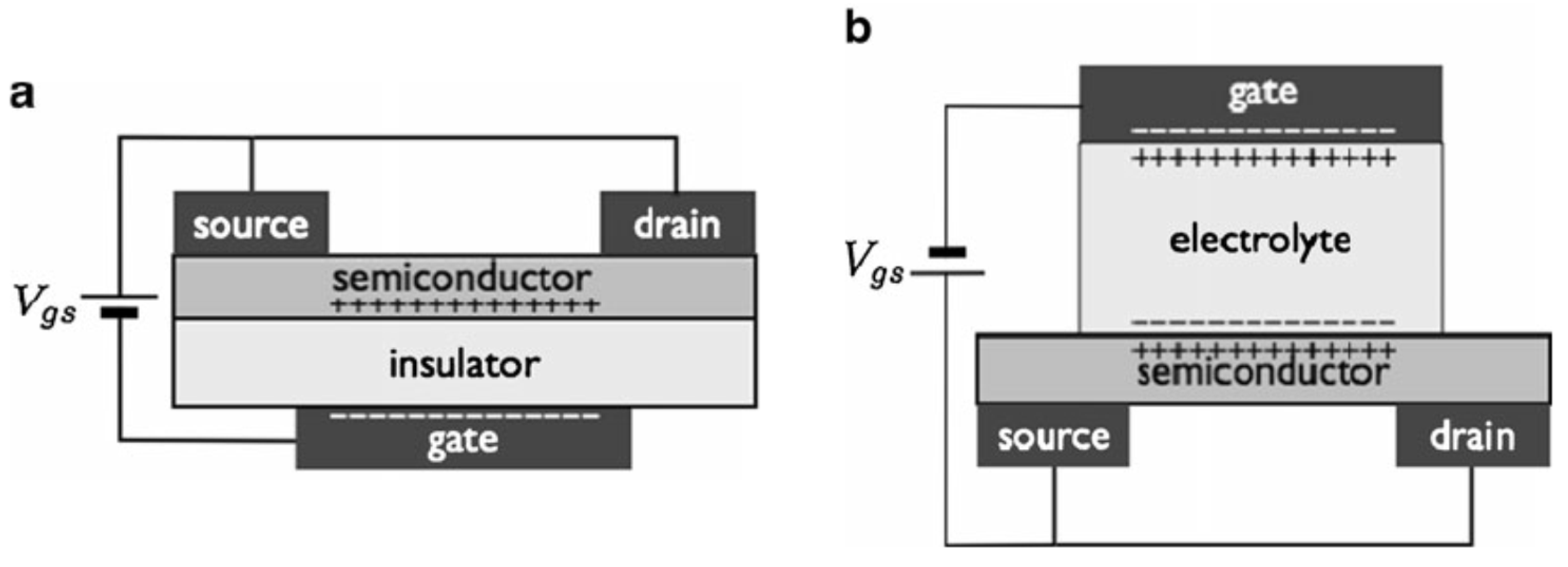
2. General Concepts of Transistors
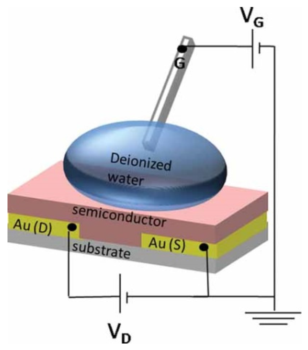
A field effect transistor (FET) is consists of three metallic conducting electrodes: source (S), drain (D) and Gate (G), a very thin insulating layer (dielectric) and a semiconductor, the latter being the active part of the device where charge carriers flow. Numerous geometries were described, among which the gate could be on top of the semiconductor (top-gate) or at the bottom of the semiconductor (bottom-gate). Similarly, the source and drain can contact the top (top-contact) or the bottom (bottom-contact) of the semiconductor. The working principle of a FET is the following: a voltage applied to the gate modifies the charge carrier density in the semiconductor in between source and drain, which therefore modulates the source-drain current. There are two kinds of charge carriers: electrons (e) and hole (h) for n or p type semiconductors, respectively. Dealing with organic FETs (OFETs), electron donating organic semiconductors involving a high highest occupied molecular orbital (HOMO) level are good candidates for p-type semiconductors, while electron-accepting ones with low HOMO levels are used as n-type semiconductors.
In OFETs, the gate is separated from the semi-conductor by an insulator. Different dielectrics can be used, e.g., oxides, polymers, self-assembled monolayers. When the gate is, for instance, negatively polarized in a p-channel device, free holes in the semi-conductor are drawn toward the semi-conductor-insulator interface to compensate an equivalent negative charge at the gate-insulator interface (Figure 1a). When a negative voltage is applied between source and drain, holes are injected from the source and current flows inside the channel. The OFET characteristics are greatly affected by the properties of the dielectric-insulator interface or at grain boundaries. The first OFET was made by Tsumura et al., in 1986, who reported a Ion/Ioff ratio (i.e., the ratio between the maximum current flowing at saturation and the minimum current when the transistor is in its blocked state) of 100, and charge carrier mobility of 10−5 cm2·V−1 [9], using a polythiophene semiconductor.

3. EGOFETs

Electrolyte-gated OFETs are significantly different from classical OFETs; indeed, the organic semiconducting layer is in contact with an electrolyte instead of a classical dielectric. In EGOFETs, the conductivity of the semiconducting channel is modulated by a solid or a liquid electrolyte put in between the semiconductor and the gate. EGOFETs display much a higher gate capacitance (up to ~1000 higher) than other types of OFETs, which use traditional inorganic or organic non-electrolytic dielectrics; as a consequence, biasing voltages used for EGOFETs are typically much smaller than those necessary for OFETs (<1 V, versus >10 V or even higher). These two characteristics (electrolyte—possibly water—and low potential) make EGOFETs ideal candidates for the next generation of biosensors, particularly suitable for the detection and quantification of biological molecules inside aqueous media. The extremely good sensing capabilities of EGOFETs rely on the possibility of properly functionalizing the gate electrode by means of specific molecules or functional groups able to interact with the target molecules present inside the electrolyte. The most common architecture is the top-gate, bottom-contact configuration. The gate electrode is immersed in the electrolyte and source and drain electrodes, isolated from the electrolyte, provide electrical contact to the channel (Figure 1b). Actually, an EGOFET looks like an OECT (organic electrochemical transistor) [10,11,12,13,14,15,16]. However, in an OECT, the on/off switch is produced by electron transfer from the electrolyte and the semiconductor (doping/de-doping) [8], whereas only capacitive processes occur for EGOFETs but no charge transfer.
In an EGOFET made with a p-type semiconductor, upon positive polarization of the gate, the anions of the electrolyte accumulate at the electrolyte/semiconductor interface while the cations accumulate at the electrolyte/OSC interface, resulting in the formation of an electrical double layer (EDL) at both interfaces. The EDL is composed of the Helmholtz layer (HL) and the diffuse layer (DL). The HL is a monolayer of ions, whereas the DL is simply more concentrated in ions (either cations or anions) than in the bulk electrolyte. In other words, the excess of ions decreases with the distance from the interface. As shown on Figure 2, when the gate is (for example) negatively polarized, the excess of electrons at the gate surface produces the accumulation of cations at the gate/electrolyte interface; conversely, accumulation of anions at the electrolyte/semiconductor interface produces accumulations of holes in the topmost layer of the semiconductor [17,18], which causes the OSC to become conducting. It has been shown that a significant double layer can form even for very low operating potentials, nevertheless sufficient to generate a locally high electrical field at the electrolyte/semiconductor interface, and therefore a high charge carrier density [8].
The electrolyte used can be polymers [19,20,21,22], ionic liquids [23,24,25] or ionic gels [16,26,27,28,29]. Aqueous liquid electrolytes were also reported. For example, Kergoat et al. [10] first reported a device gated with water (Figure 3). By replacing the gate dielectric by a simple water droplet, they produced a transistor that entirely operates in the field-effect mode at voltages lower than 1 V. They have shown (unpublished results) that the electrical characteristics do not depend on the pH in a range between 4 and 8, which is well adapted to biomolecules.
This result creates opportunities for sensor applications. Indeed, water is the natural environment for biological receptors [30]. In this case, water must act both as the electrolyte and the media responsible for carrying the analytic sample, which is the current challenge to develop EGOFET-based biosensors. However, in such conditions, an electrochemical doping (i.e., insertion into the semiconductor of ions from the electrolyte) may occur, which decreases the capacitance and the field effect and therefore degrades the semiconductor electrical properties. This is the main reason why the performances of EGOFET often decrease dramatically upon use [31,32]; this constitutes an important issue that must be addressed; for example, by developing highly hydrophobic polymeric OSC. However, some small analytes or even ions have no problems to pass a thin hydrophobic barrier. High crystallinity of the organic semiconductor can suppress diffusion of such species. Since most polymer films are semi-crystalline at best, this might be an aspect where crystalline films made from small molecules might be superior in terms of blocking and should be investigated. Another issue that must be addressed is their high subthreshold swing, typically of several hundreds of millivolts, which impede their sensitivity. A strategy may be to switch from classical OSC to graphene-based materials, e.g., graphene or reduced graphene oxide, which has already been reported [33,34,35,36,37,38,39,40,41,42,43,44,45,46], but this will not be discussed here. Readers who are interested in grapheme-based EGOFETs may report on the review from Yan et al., 2013, which dealt with graphene-based transistors for biological sensors [47]. However, graphene has been shown to have low sensitivity due to lack of bandgap. For this reason, other electrolyte-gated inorganic FETs are also promising, for example based on MoS2 semiconductor [48]. In EGOFETs, the gate material also influences the figures of merit of the devices, particularly the threshold potential VT [49,50]. However, most of the transistor characteristics come from the semiconducting material itself and from the quality of the contact between the source and drain electrodes and the OSC. This quality noticeably depends on the way the semiconductor is deposited.

4. Semiconducting Materials

4.1. Deposition Techniques

Several deposition techniques were described; among them: spin coating, vacuum thermal deposition, printing and spray deposition. Spin-coating and drop-casting remain the most popular in laboratory, whereas inkjet printing and spray deposition are preferentially used in industry; vacuum thermal evaporation is used in both environments.

4.1.1. Vacuum Thermal Evaporation

For vacuum thermal evaporation, both the semiconducting material and the substrate are placed in high vacuum. The OSC is thermally sublimated then is condensed on the cold substrate to form a film, the thickness of which being controlled by the deposition time and the temperature [51,52].

4.1.2. Spin-Coating

Spin-coating consists of spinning the substrate onto which a solution containing the semiconducting material is deposited. Spinning produces a centrifugal force that homogeneously spreads the solution and forms a very thin film over the substrate; its thickness is a balance between the centrifugal force and the solution viscosity. During this operation, the solvent evaporates, leaving a thin film of semiconducting material. An additional annealing step is needed to crystalize the semiconductor molecules, which improve the electrical performances [53,54]. Very roughly, the film thickness depends on the concentration of the solution (the more concentrated, the thicker), the rotation speed (the faster, the thinner) and the evaporation rate of the solvent (the faster, the thicker). Compared to vacuum thermal evaporation, the advantage of spin-coating is that it does not need heating, which avoids thermal degradation of semiconductors. The main limitation is that all semiconductors cannot dissolve in volatile solvents.

4.1.3. Inkjet Printing and Spray Deposition

Inkjet printing is a non-contact solution-processed technique which allows non-lithographic patterning, for a lateral resolution as small as 5 μm, however depending on substrate preparation [55,56]. Inkjet printing is an additive technology and is therefore much less wasteful than other solution-based methods using subtractive patterning methods; it generally ensures a better electrical contact with the underlying electrode/material than the vacuum thermal evaporation [57] but it has the disadvantages of poor lateral resolution compared to lithography [31,58,59,60].
Spray deposition is another non-contact solution-based method. In this case, instead of thermal of piezoelectric propulsion of the ink, the liquid is pumped and guided through a gas flow to the substrate. Like for inkjet-printing, the ink arrives at the substrate as micrometric droplets. For this reason, a challenge for both techniques is to achieve uniform films [52,61].

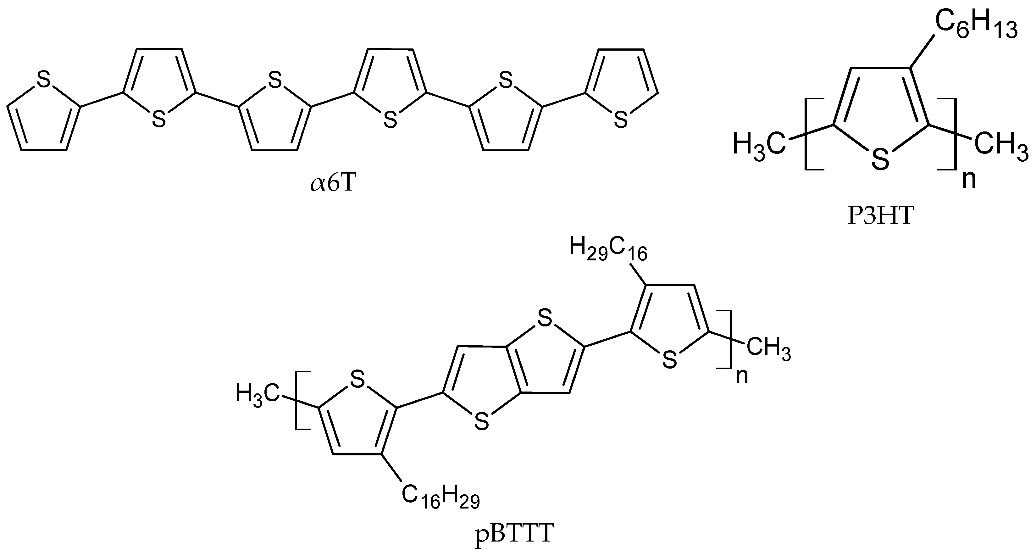
4.2. Semiconducting Materials

4.2.1. Generalities

It is remarkable to note that no rationale has been published concerning chemical stability of OSCs applicable in EGOFETs. One may keep in mind that the highest occupied molecular orbital (HOMO) and lowest unoccupied molecular orbital (LUMO) levels of the OSC should not allow electrolyte oxidation or reduction; another very important parameter is that the electrolyte should not penetrate into the OSC, which would become electroactive. Even though Buth et al. used α-sexithiophene (α6T) in 2011 and 2012 to make an EGOFET-based biosensor [11,62], most EGOFET biosensors were reported with poly(3-hexylthiophene) (P3HT) as the organic semiconductors [8,32,60,63,64,65,66,67,68,69,70,71,72]. In recent years, thienothiophene copolymers [73], especially the poly(2,5-bis(3-alkylthiophen-2-yl)thieno[3,2-b]-thiophene) (pBTTT) was also considered, due to a better stability in humid environment or even in water (Figure 4) [74,75,76,77].

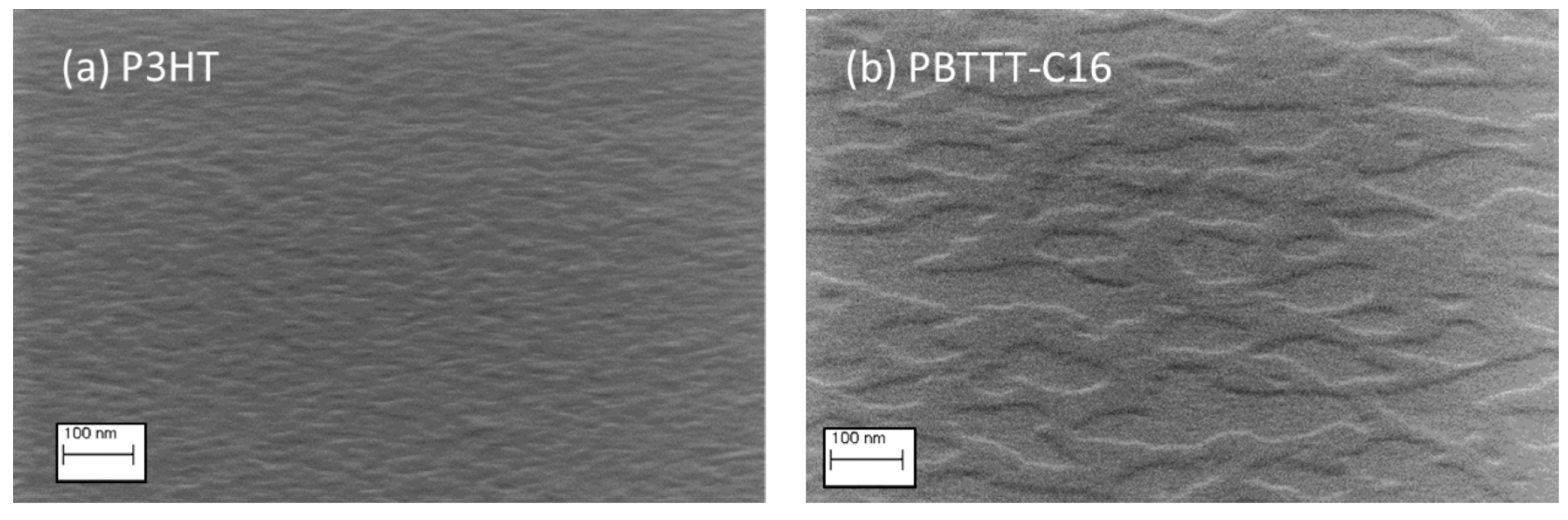
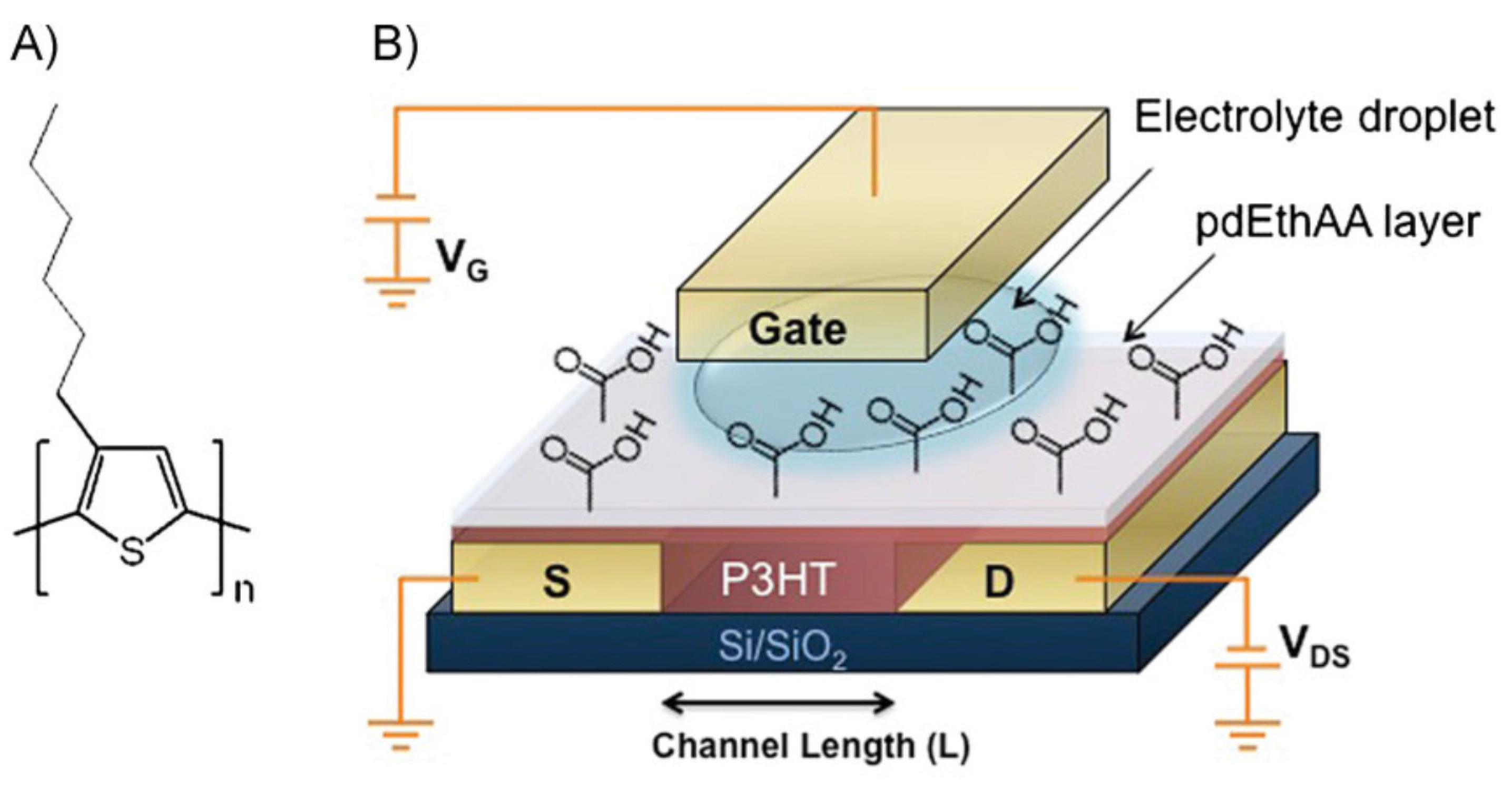
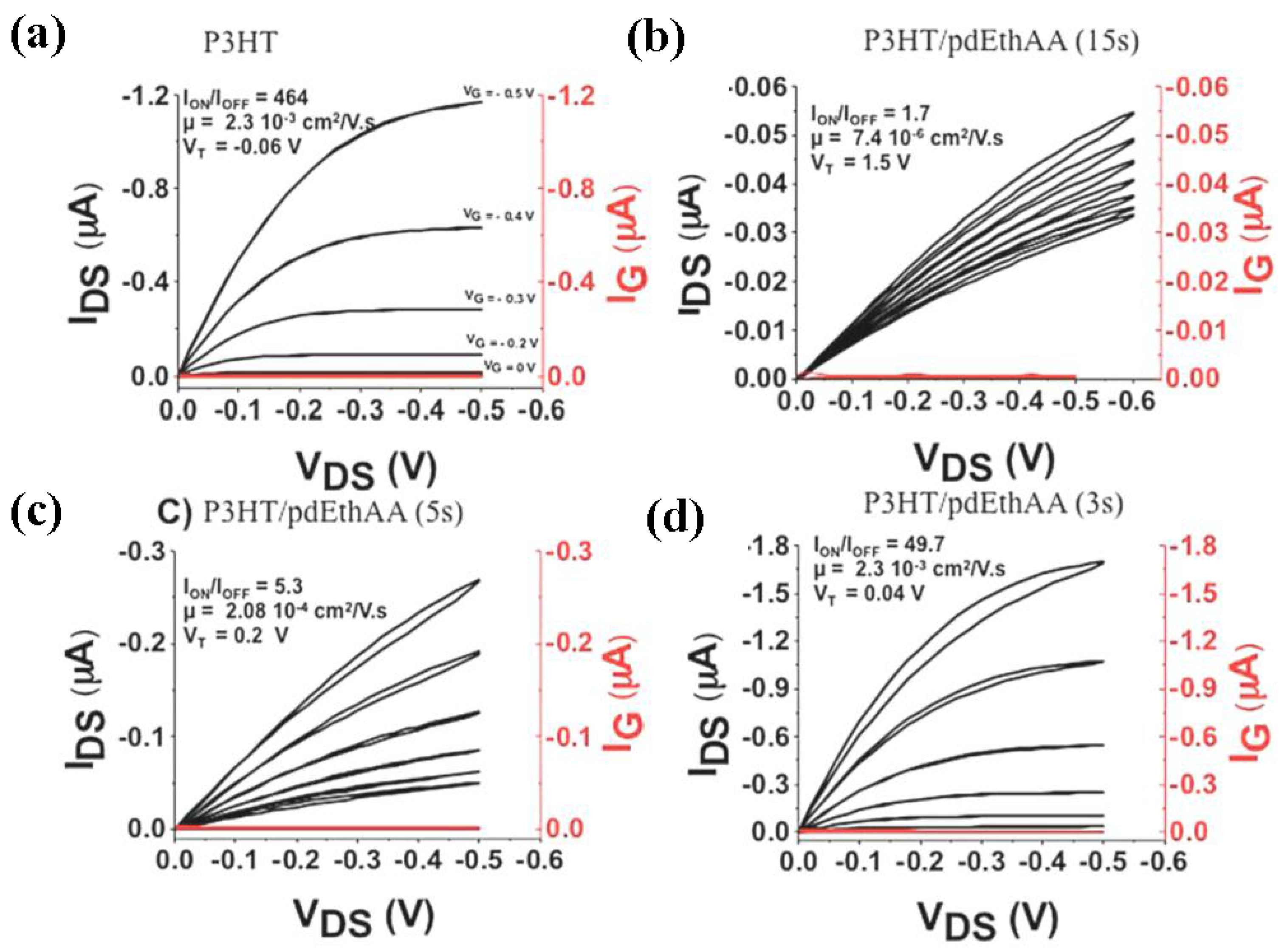
4.2.2. Poly(3-hexylthiophene) (P3HT)

P3HT is the most common OSC used during the last decade [19]. Kline et al. analyzed a series of regioregular polythiophenes on an OTFT device. They found that the crystallinity and molecular weight are two important parameters on the hole mobility, resulting from the well-defined molecular architecture of P3HT [78]. For example, 3-hexylthiophene units may polymerize through head-to-tail, head-to-head or tail-to-tail couplings; the percentage of head-to-tail coupling represents the degree of regioregularity of P3HT, which is critical to the electronic properties of the material. High-performance OFETs based on highly regioregular P3HT were successfully fabricated by solution process and showed hole mobilities higher than 0.1 cm2/Vs and very high on/off ratios (>105) [79].
If P3HT is deposited by spin-coating, the best solvent is chloroform, due to its rapid evaporation which limits crystallization during the spin-coating process [79,80]; this impose a thermal post-treatment process able to favor crystallization and π−π stacking of the P3HT backbone. It has been shown that this results in a lamellar structure formed by interchain stacking (Figure 5). It has also been shown that the hole mobility varies by two orders of magnitude depending on orientation (parallel or normal to the substrate) of the lamellae [53,54,81,82,83,84,85,86], the normal one giving the highest mobility.
According to the work of Alberga et al. [53], spin-coated then annealed P3HT displays three different zones: an interfacial zone close to the substrate (thickness of 10 Å), an intermediate zone 30 Å thick atop and an OSC/electrolyte interfacial zone over this distance; the first layers display the highest degree of order [53,87,88,89].
Some strategies were proposed to improve the performance and/or biocompatibility of P3HT. For example, Liu et al. printed P3HT above another terrylene semiconductor to make a heterojunction of semiconductor [57]. Thiemann et al. spray-coated a layer of ion gel based of silane-ionic liquids on P3HT to obtain advantageous properties such as low modulus, solution processability and high specific capacitance [61]. Magliulo et al. modified the surface of P3HT by plasma-enhanced vapor chemical deposition (PE-CVD) of a mixture of ethylene, acrylic acid and argon in a 1:3:1 ratio, which increased the –COOH content at the surface, eventually used to covalently graft phospholipids on the OSC, themselves used to bind biological molecules [64,71,90]. Kergoat et al. [91], Sinno et al. [59] and Toss et al. [92] used chemical reactions to bind P3HT with another polymer to make new semiconductor polymer blends with improved stability, electronic performances and biocompatibility. Suspène et al. used peptidic coupling to directly graft biotin on P3HT in order to make a proof-of-concept streptavidin or avidin sensor [93]. All these approaches impose making compromises between the electrical and immobilization properties.

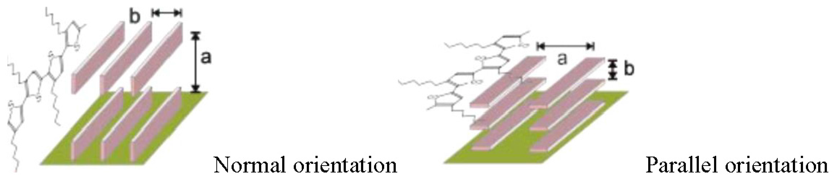
4.2.3. Poly(2,5-bis(3-alkylthiophen-2-yl)thieno[3,2-b]-thiophene) (pBTTT)

Even if P3HT is certainly the mostly used semiconductor in OFETs, its instability is well known, which obviously limits its utilization for biosensors [94,95,96]. pBTTT has recently attracted attention as another promising solution-processed semiconducting polymer. pBTTT shows better performances than P3HT (hole mobility up to 1.0 cm2/Vs for pBTTT versus 0.1 cm2/Vs for P3HT [97,98]), less electrochemical doping and much better stability in aqueous environment [53,99].
Liquid-crystalline pBTTT was firstly used as semiconductor layer in liquid-gated structure by Naim et al. [100]; Chao et al. show that pBTTT has a similar lamellar structure than P3HT [101]; however, pBTTT has larger crystalline domains extended over several hundreds of nm [75,96,98] (Figure 6). This probably explains why pBTTT has better performances [102,103].
The best solvent for spin-coating pBTTT is chlorobenzene. It was shown that, because the boiling point of chlorobenzene is high, few residual solvent molecules may remain after annealing, and these solvent molecules may behave as plasticizer, increase free space between chains thus facilitate orientation and crystallization [53,98,102].

5. Biosensors with EGOFETs

Hereafter are reviewed the various EGOFET-based biosensors reported in the literature since 2012.

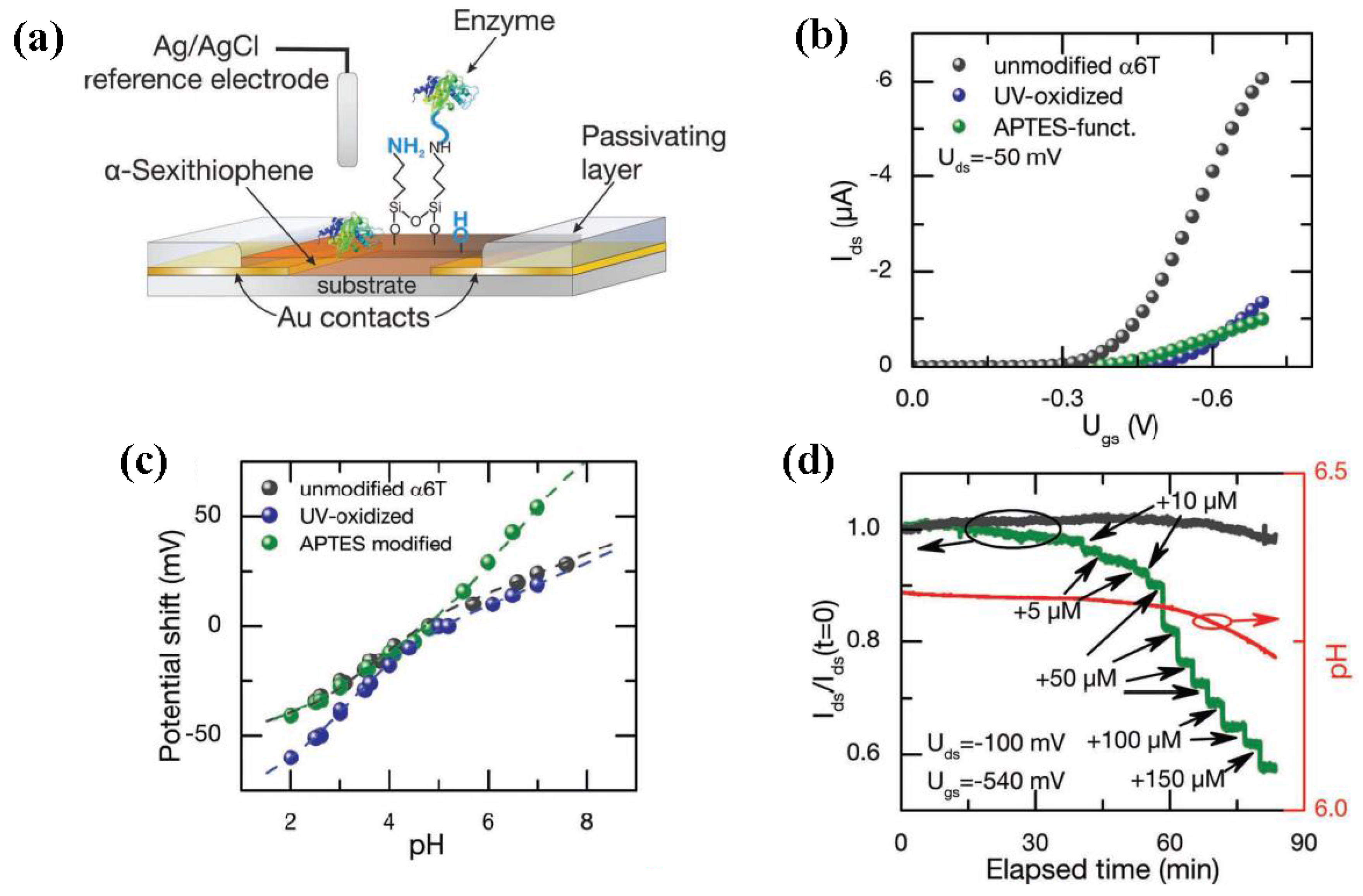
5.1. α-Sexithiophene (α6T)-Based EGOFET Sensor for Detection of Enzyme Activity

Buth et al. described in 2012 [11] an EGOFET which they named solution-gated organic field-effect transistors. The semiconductor (α-sexithiophene) surface was modified by –OH or –NH2 groups, leading to a pH sensor operating in a pH range relative to the pKa of the added surface functions. The hydroxyl groups were added by oxidation under UV, and the amine groups were added by grafting 3-aminopropyltriethoxysilane. The on/off ratio at VDS = −50 mV was between 102 and 103, with a field-effect mobility of 4 × 10⁻² cm2·V−1·s−1. The authors found a sensitivity of 14 mV·pH−1. As a proof-of-concept, they immobilized the penicillinase enzyme on the semiconductor and sensed penicillin (Figure 7) by the way of an acid-base titration. They found a detection limit of ca. 5 μM. At low penicillin concentration, the sensitivity of the device was ca. 80 μV·μM−1.

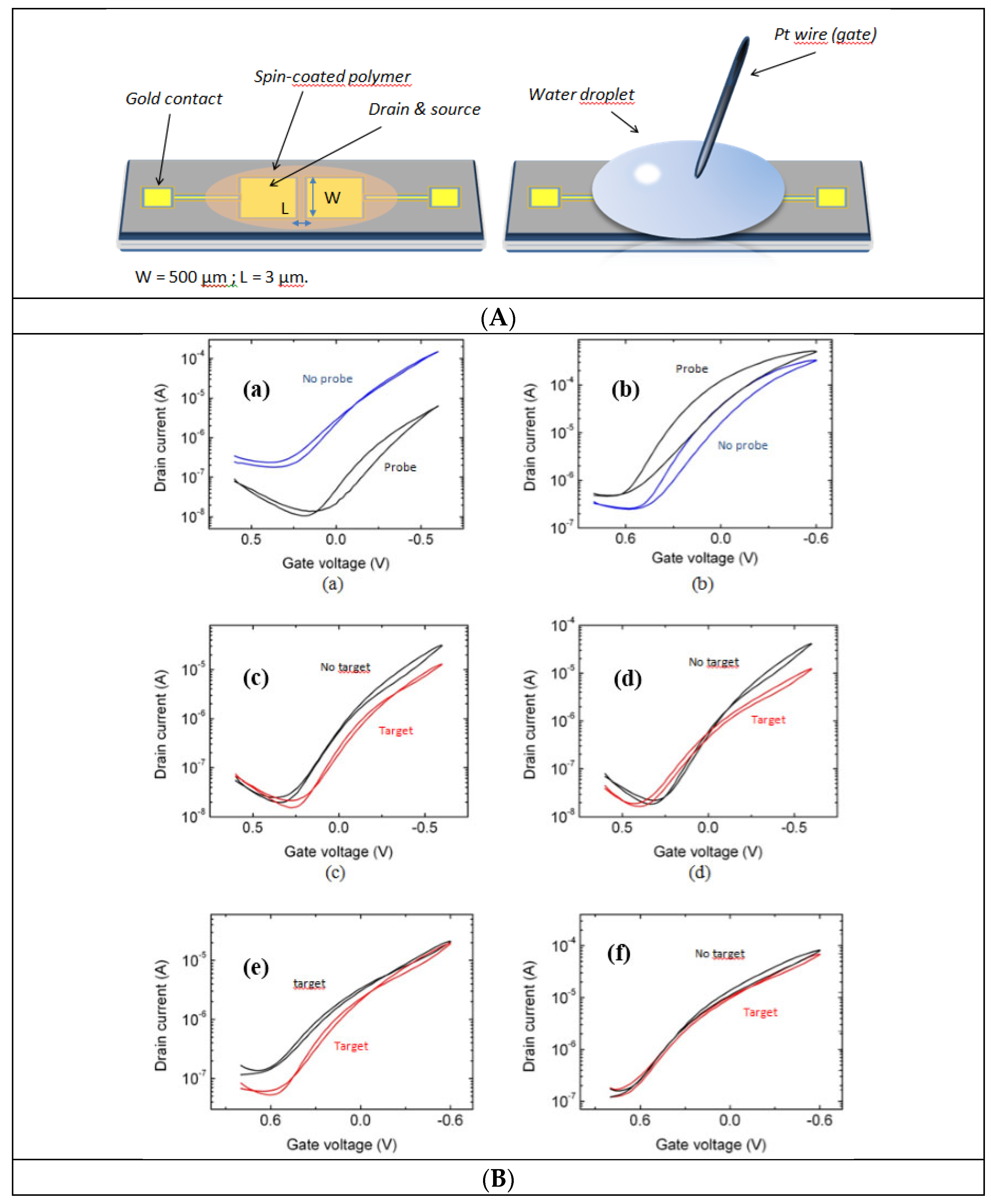
5.2. P3HT-Based EGOFET Sensor for DNA Detection

A DNA EGOFET sensor was first reported by Kergoat et al. [70] (Figure 8A), in which the dielectric is constituted by a simple droplet of aqueous phosphate buffer saline (PBS, pH 7.2) solution. This device allows operating at very low voltages (below 1 V). This renders possible the use of buffer solutions within their electrochemical stability window. A P3HT bearing carboxylic acid moieties was used to perform covalent ODN (oligonucleotide) grafting, providing that they are modified at one end with a –COOH group. Changes in the output characteristics of the device were observed upon DNA immobilization and after DNA hybridization (Table 1), of 40 to 60 mV of gate voltage shift for 100 nM target DNA. This shift towards negative values was attributed to the negative charge of the DNA backbone. The off current was also modified and decreased after DNA immobilization. This behavior was attributed to the steric hindrance of DNA chains that eventually prevents ion penetration into the bulk of the semiconductor (Figure 8B). Other experiments, obtained with various ionic strength, pointed out the importance of the Debye length that can screen negative DNA charges.
Schmoltner et al. reported an EGOFET based on P3HT for which they investigated the effect of the gate material (as in ref. [10]) and of the ionic strength of the electrolyte on the device performances [104]. Magliulo et al. published in 2013 a work where they demonstrated PE-CVD of an hydrophilic thin layer (plasma deposited ethylene/acrylic acid (pdEthAA)) carrying COOH groups on P3HT (Figure 9) [71]. The thickness of the coating was particularly monitored because it should be minimized to avoid adverse effect on the EGOFET performance. A comparison between pristine P3HT and pdEthAA/P3HT bilayer is given on Figure 10. It is also shown on this figure that the gate current (IG, red curves and right Y-scale) stay low, which demonstrates the field-effect mode of operation and excludes the electrochemical mode of operation; this shows that the hydrophobic layer fully plays its role by impeding ion penetration in the OSC. In addition, the authors reported that chemical or biological species could be covalently immobilized on such functional hydrophobic/hydrophilic bilayer, such as DNA probes (even if not described in their article).

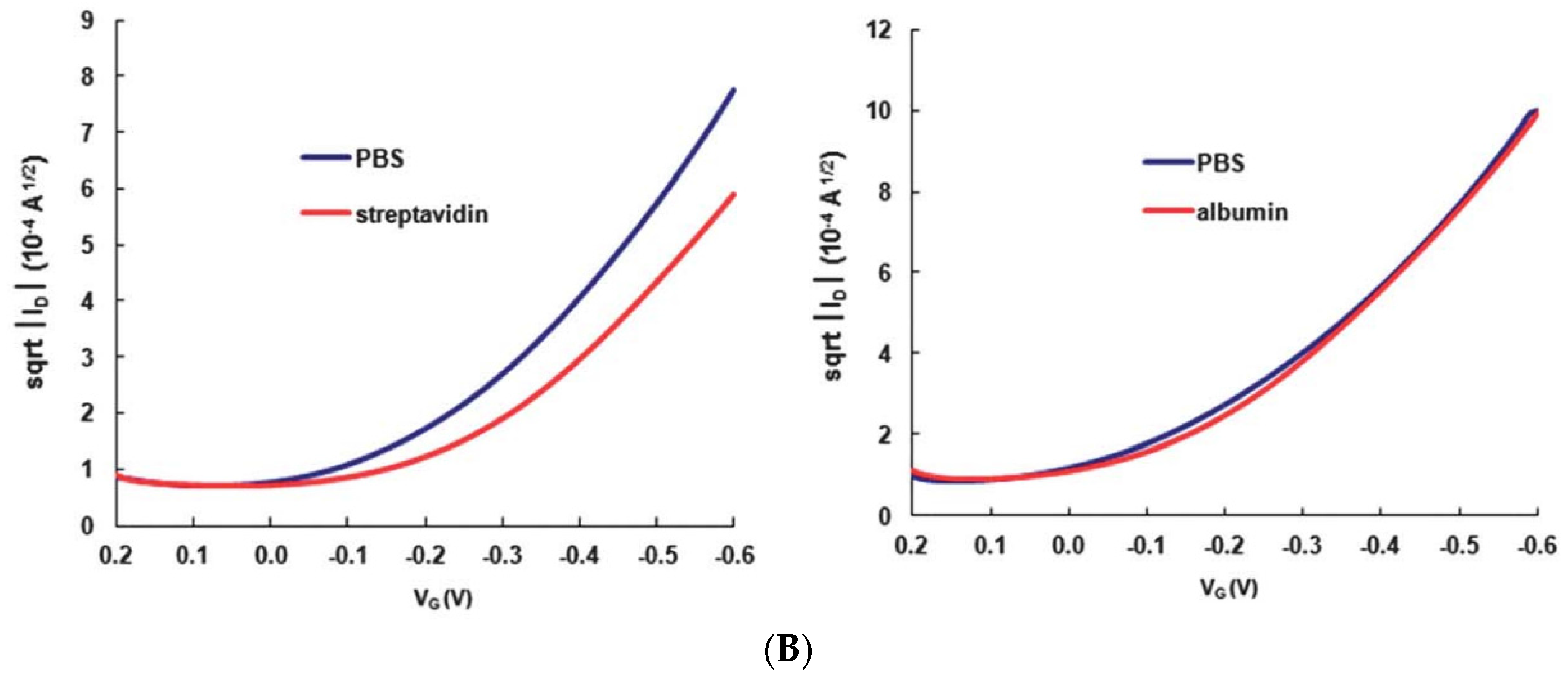
5.3. P3HT-Based EGOFET for Protein (Streptavidin) Detection

Suspene et al. reported in 2013 on the sensing of streptavidin with an EGOFET using a copolymer of P3HT, P3HT-COOH and biotinylated P3HT (Figure 11A) as the active sensing and semiconducting material [93]. The biotin-streptavidin couple was chosen as a proof-of-concept, for its extremely low dissociation constant. Non-specific interactions were reduced due to the presence of the COOH function; it was further reduced when the polymer surface was pretreated with 1-octanol, which interacted non-covalently with P3HT with its C8 alkyl chain. In this case, human serum albumin had no effect on the transistor characteristics, whereas streptavidin led to a decrease of the drain current (Figure 11B).
In order to investigate the transduction mechanisms of such EGOFET devices, Palazzo et al. [30] investigated in 2014 the sensitivity of their EGOFET as a function of the Debye’s length, the receptor charge, and the distance at which the binding event takes place. For this, they used biotin/avidin and antigen/antibody interactions (C-reactive protein CRP and anti-CRP, respectively). The sensor was shown to successfully detect binding events occurring at distances that are 30 times the Debye’s length value from the transistor electronic channel, and even to deliver higher responses in the presence of high salt concentrations (Figure 12A). The sensitivity was not calculated, but the limit of detection was ca. 10 μg·mL−1 of CRP. Transduction of the molecular recognition was explained by capacitance changes at the electrolyte/OSC interface rather than by electrostatic effects of the charges carried by the target molecules (Figure 12B).

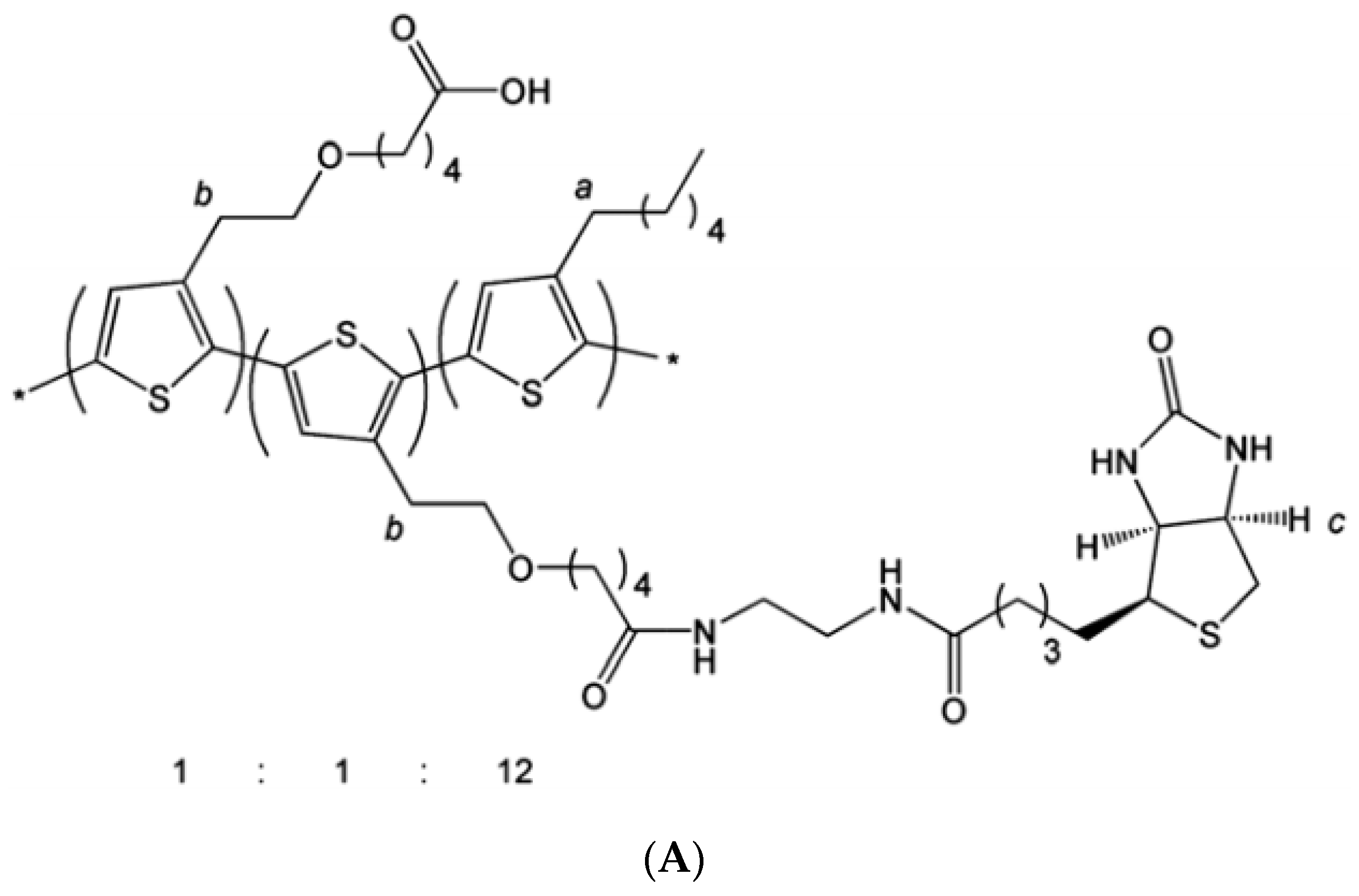
5.4. Non-Covalent Functionalization of the Semiconductor

Still with the objective to functionalize the semiconductor and impede its doping by ions present in the electrolyte, Cotrone et al. described a non-covalent approach using a phospholipid bilayer [93]. They compared the electric performances of the EGOFET including a phospholipid film to those with the organic semiconductor directly in contact with the gating solution. Impedance spectroscopy was employed to show that this phospholipid bilayer minimizes the penetration of ions into the OSC thus improves the field-effect mode of operation and discriminates the electrochemical one. No bioprobes were immobilized on or into this bilayer but this work is a significant step toward EGOFETs biocompatibilization.
One year later [64], Magliulo et al. used biotin-labeled phospholipids, in order to form a streptavidin binding layer (Figure 13). They achieved detection with a LoD of 10 nM even in a high ionic strength solution. They attributed the sensing mechanism to the capacitive effect across the phospholipid bilayer, involving the charges carried by streptavidin. Because the biotinylated phospholipid can easily be functionalized with virtually any receptors, this work paved the way for immunosensors, capture antibodies usually being modified by streptavidin for hetergeneous ELISA immunoassay.

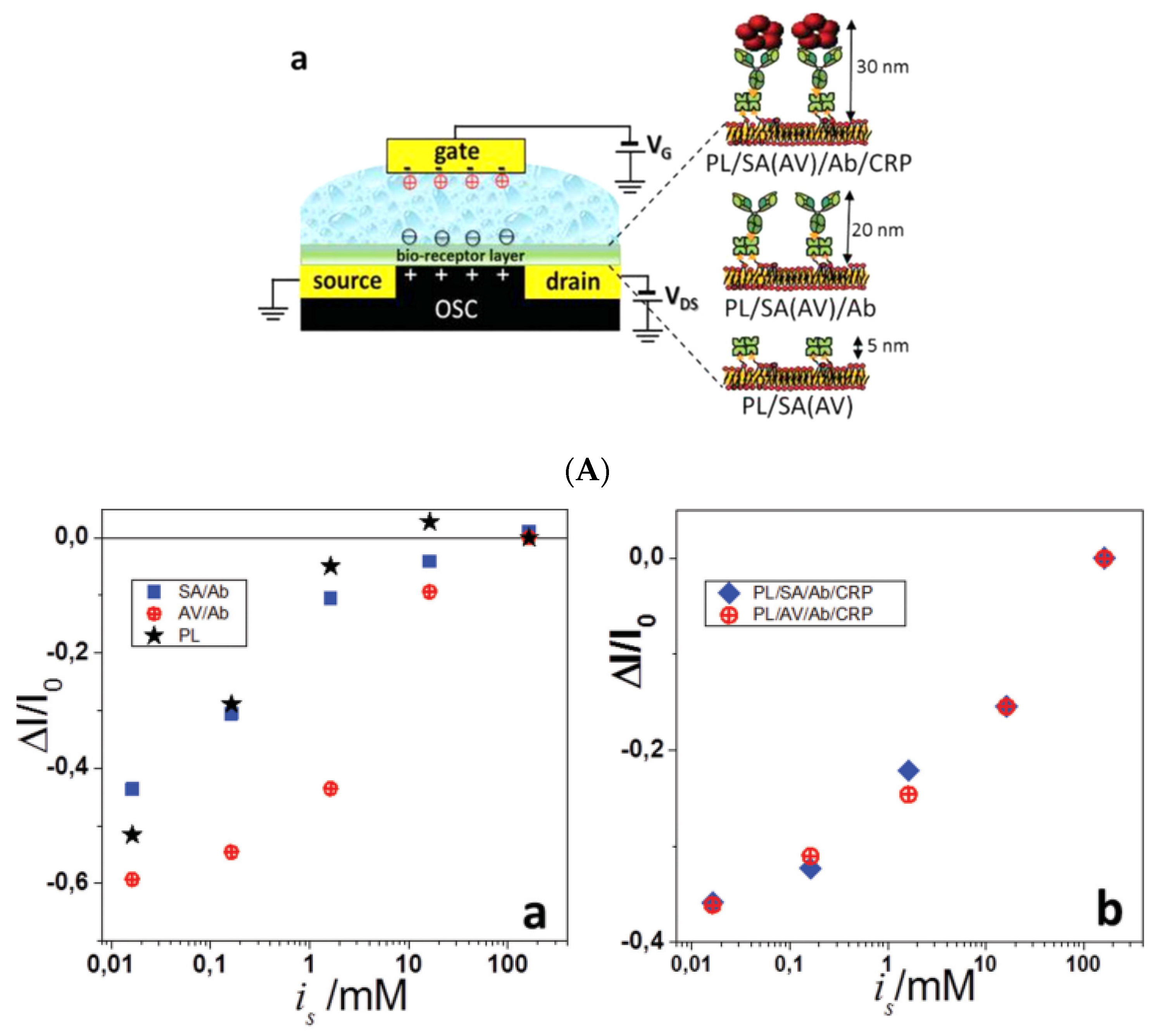
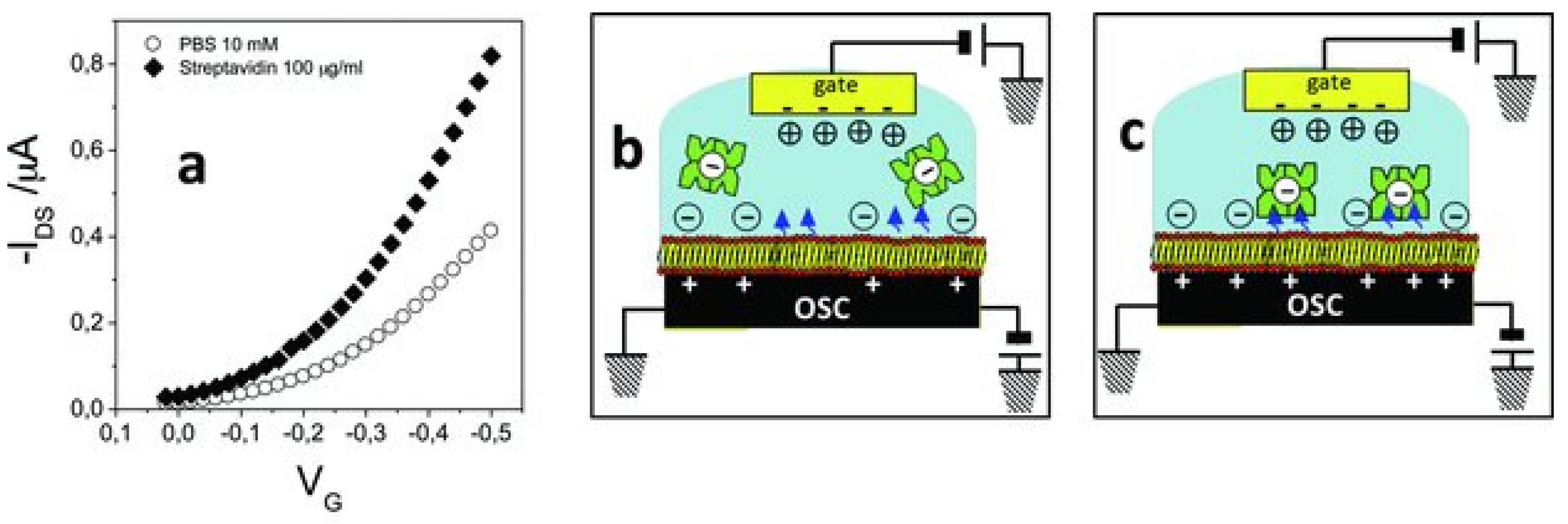
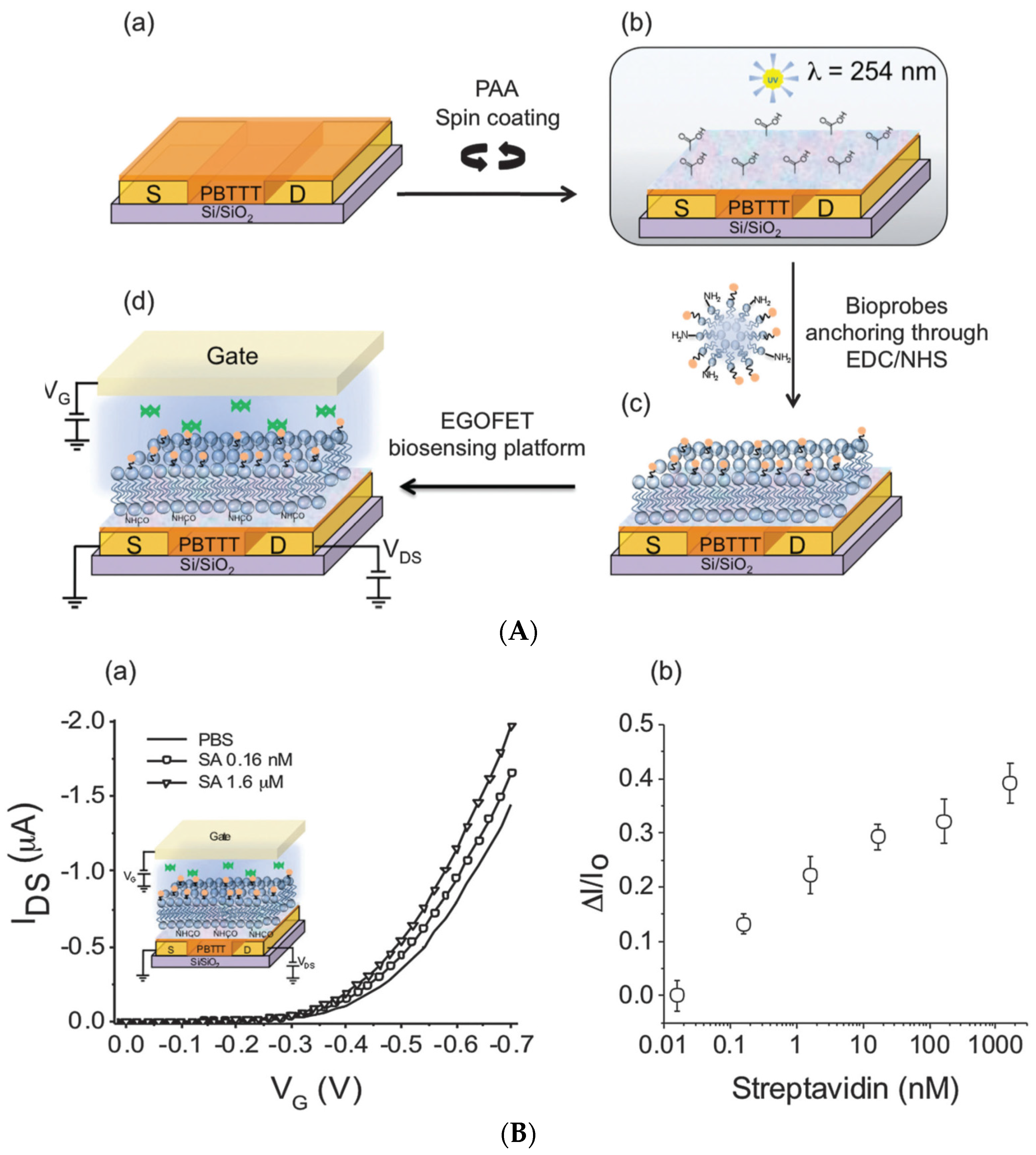
5.5. pBTTT-Based EGOFET for Protein (Streptavidin) Detection

Mulla et al. [76] reported a pBTTT-based EGOFET sensor for streptavidin detection. pBTTT was spin-coated on the device, then a layer of poly(acrylic acid) was spin-coated on the pBTTT layer to have carboxyl functionalities acting as anchoring sites for phospholipid bilayers. The proof-of-concept of the sensor was demonstrated with the streptavidin/biotin couple (Figure 14).

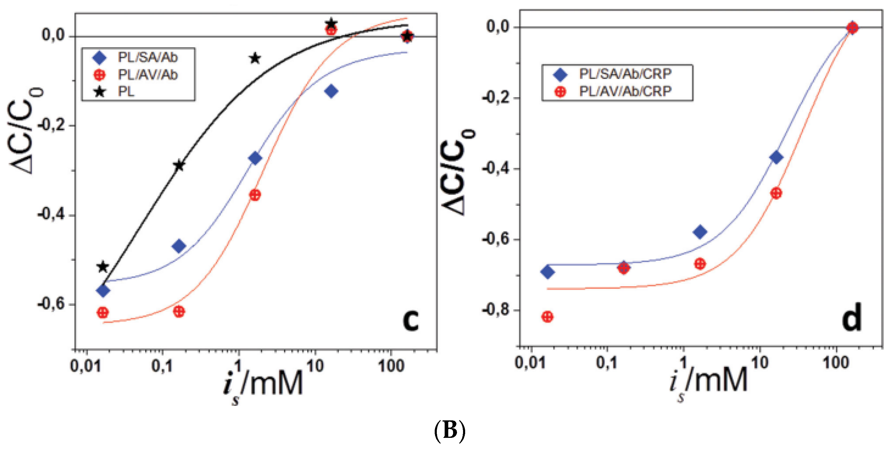
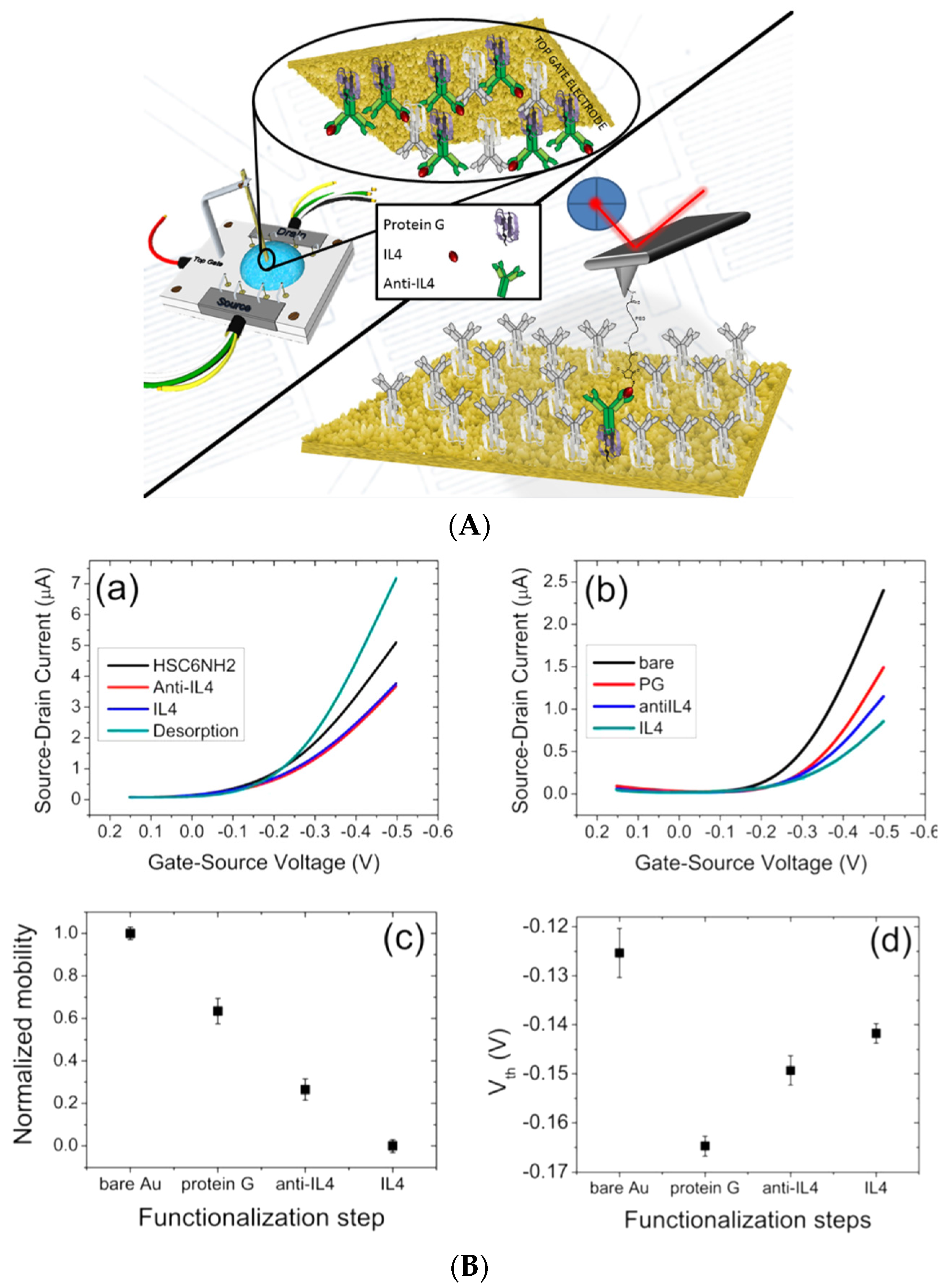
5.6. Gate Functionalization

Casalini et al. [32] reported in 2013 a P3HT-based EGOFET biosensor for dopamine detection where a gold gate was used as the sensing area instead of the semiconductor. They modified the gate/electrolyte interface with a self-assembled monolayer of cysteamine and 4-formylphenyl boronic acid. This modified gate enabled the selective covalent binding of dopamine that, in turn, modulates both the work function of the gate electrode and the capacitance of the electrode/electrolyte double layer. The strong dependence of the EGOFET transfer curve upon dopamine coupling at the gate electrode is a proof of its sensitivity to small changes in gate capacitance. For dopamine detection, the threshold voltage shift was of ca. 50 mV for 0.1 nM dopamine. The selectivity of boronic acid for dopamine was supported by the fact that boronic acid is known to act as a Lewis acid for association with vicinal glycols such as sugars or catechol, via formation of a boronate ester. This reaction also works well on dopamine and is therefore specific, providing that no other vicinal diols are present in the analyzed sample (this reaction has been often reported in the literature dedicated to dopamine sensing since 2013).
Casalini et al. [105] published more recently another work using Au gate as sensing area, instead of the semiconductor, using thiol-modified protein G or a 6-aminohexanethiol (HSC6NH2) self-assembled monolayer followed by covalent coupling (protein G was used here for its property to bind IgG antibodies). They found that the most sensitive EGOFET was obtained with the first (affinity) immobilization strategy. They explained this result by the best orientation of the antibodies on the gate surface, which they probed by force spectroscopy (Figure 15). The lowest concentration of antigen (interleukin, IL4) that was detected was ca. 5 nM. These results, and particularly the coupling between sensing experiments and surface characterizations, were very powerful to rationalize the response of an EGOFET using antibodies grafted on the gate.
Mulla et al. [77] also described an EGOFET where the gate was the sensing element. They immobilized proteins on the Au gate through a self-assembled monolayer and showed that the transduction capability of the device was governed by the capacitance of the gate/electrolyte interface. The authors applied this architecture to the detection of odorant molecules (Figure 16), by following drain current as a function of the target molecule concentration (carvone). The sensor presented a limit of detection estimated around 10 pM and was enantioselective.

5.7. Other Type of Electrolyte

More sophisticated electrolytes can be used in EGOFETs in order to maximize the capacitance changes upon a molecular recognition event. Even if their work has not been significantly cited yet, Lee et al. introduced this concept in 2013 [106]. They used bovine serum albumin (BSA) as electrolyte, because BSA has good hydration ability, containing a high percentage of acidic and basic amino acid residues. They showed that, in dry state, BSA-gated pentacene OFETs exhibited a threshold voltage of ca. −16 V, whereas the VTH was reduced to −0.7 V under humid conditions.
Very recently, Dumitru et al. [107] used a pH-sensitive alginate hydrogel as electrolyte (Figure 17a,b), which is biocompatible and biodegradable. To demonstrate the efficiency of such hydrogels to host bioreceptor without damaging its bioactivity, glucose oxidase was entrapped into the alginate in order to make a biosensor. The enzyme activity, producing an acidification of the medium through transformation of glucose into gluconic acid, modified the gel swelling (polymer chains conformational switch) that lead to a capacitance modulation and therefore a field effect change (Figure 17e). The sensitivity toward glucose was not given.

5.8. Use of Nanoparticles

The use of nanoparticles (NPs) has not been reported yet in EGOFET devices for biosensing. However, NPs have been extensively reported in other type of biosensors for years, mainly because NPs provide an extremely high surface-to-volume ratio, i.e., a high specific active area, which makes bioprobes more accessible than on a planar surface. In addition, because EGOFETs are sensitive to capacitance changes (a typical surface effect), NPs should be extremely pertinent in EGOFETs. As an example of what could be done, Poghossian et al., not in an organic-based but in a silicon-based device, reported a gating capacitive field-effect sensor [108] for detection of charged molecules using gold NPs to increase the capacitive effect (Figure 18). Bao’s group also reported biodetection using a classical bottom-gate OFET decorated with gold nanoparticles, which were used to vary spacing between receptors [109].

6. Conclusions and Outlooks

In this review, we presented recent advances in electrolyte-gated field-effect transistors applied for biosensors. EGOFETs rely on the accumulation of charges at the gate/dielectric and dielectric/semiconductor interfaces. The detection principles in EGOFETs are based on changes of these surface capacitances induced by the biological recognition between probe and target molecules. The electrolyte, which replaces the classical dielectric in EGOFET, fits well with biological processes (which generally take place in water), whereas it is less straightforward to apply regular dielectric-based OFETs for biosensing. There is still a lot of work to do to improve EGOFET-based biosensor’s performances. The most challenging is certainly the stability of the semiconductors in water or neutral buffers, the immobilization of the bioprobes whether onto the gate or the semiconductor surface, and a better understanding of the operating principles for the design of more efficient transduction architectures. Concerning OSC, only few were used until now (P3HT, pBTTT, α-sexithiophene, and pentacene) and many others deserve to be investigated. Concerning immobilization, different methods were used to immobilize the biological probes on the sensing parts of EGOFETs, whether by covalent or non-covalent methods. Covalent bindings look to be more efficient on the gate, whereas non-covalent immobilizations are more convenient on the semiconductors because it avoids tedious chemical derivatization, which generally impedes the electrical performances of the OSC. Most biorecognition processes reported in the literature concern DNA hybridization, specific chemical couplings, DNA or peptide aptamers, antibody–antigen recognitions or other protein–protein interactions. Most of these methods involve capture of a free target in electrolyte onto a biological probe immobilized on a surface. However, an opposite way of thinking, inspired from competitive immunoassays, is also a promising approach, worth trying. At last, nanostructuration of gates or semiconductors should be investigated.

Acknowledgments

D.W. thanks the Doctorate School ED388 for a Ph.D. grant.

Author Contributions

The authors contributed equally to the writing of the manuscript.

Conflicts of Interest

The authors declare no conflict of interest.

References

  1. Wilkinson, A.; McNaught, A.D. IUPAC Compendium of Chemical Terminology, (the “Gold Book”); Blackwell Scientific Publications: Oxford, UK, 1997. [Google Scholar]
  2. Nic, M.; Jirat, J.; Kosata, B. Compendium of Chemical Terminology; Blackwell Scientific Publications: Oxford, UK, 1997; Available online: http://goldbook.iupac.org (accessed on 23 Feburary 2016).
  3. Thévenot, D.R.; Toth, K.; Durst, R.A.; Wilson, G.S. Electrochemical biosensors: Recommended definitions and classification. Biosens. Bioelectron. 2001, 16, 121–131. [Google Scholar] [CrossRef]
  4. Clark, L.C.; Lyons, C. Electrode systems for continuous monitoring in cardiovascular surgery. Ann. N. Y. Acad. Sci. 1962, 102, 29–45. [Google Scholar] [CrossRef] [PubMed]
  5. Amos, S.W.; James, M. Principles of Transistor Circuits; Butterworths: London, UK, 1984. [Google Scholar]
  6. Strakosas, X.; Bongo, M.; Owens, R.M. The organic electrochemical transistor for biological applications. J. Appl. Polym. Sci. 2015, 132. [Google Scholar] [CrossRef]
  7. Sarkar, D.; Banerjee, K. Proposal for tunnel-field-effect-transistor as ultra-sensitive and label-free biosensors. Appl. Phys. Lett. 2012, 100, 143108. [Google Scholar] [CrossRef]
  8. Kergoat, L.; Piro, B.; Berggren, M.; Horowitz, G.; Pham, M.-C. Advances in organic transistor-based biosensors: From organic electrochemical transistors to electrolyte-gated organic field-effect transistors. Anal. Bioanal. Chem. 2012, 402, 1813–1826. [Google Scholar] [CrossRef] [PubMed]
  9. Tsumura, A.; Koezuka, H.; Ando, T. Macromolecular electronic device: Field-effect transistor with a polythiophene thin film. Appl. Phys. Lett. 1986, 49, 1210–1212. [Google Scholar] [CrossRef]
  10. Kergoat, L.; Herlogsson, L.; Braga, D.; Piro, B.; Pham, M.C.; Crispin, X.; Berggren, M.; Horowitz, G. A water-gate organic field-effect transistor. Adv. Mater. 2010, 22, 2565–2569. [Google Scholar] [CrossRef] [PubMed]
  11. Buth, F.; Donner, A.; Sachsenhauser, M.; Stutzmann, M.; Garrido, J.A. Biofunctional electrolyte-gated organic field-effect transistors. Adv. Mater. 2012, 24, 4511–4517. [Google Scholar] [CrossRef] [PubMed]
  12. Dhoot, A.S.; Yuen, J.D.; Heeney, M.; McCulloch, I.; Moses, D.; Heeger, A.J. Beyond the metal-insulator transition in polymer electrolyte gated polymer field-effect transistors. Proc. Natl. Acad. Sci. USA 2006, 103, 11834–11837. [Google Scholar] [CrossRef] [PubMed]
  13. Tarabella, G.; Mohammadi, F.M.; Coppedè, N.; Barbero, F.; Iannotta, S.; Santato, C.; Cicoira, F. New opportunities for organic electronics and bioelectronics: Ions in action. Chem. Sci. 2013, 4, 1395–1409. [Google Scholar] [CrossRef]
  14. Kim, S.H.; Hong, K.; Xie, W.; Lee, K.H.; Zhang, S.; Lodge, T.P.; Frisbie, C.D. Electrolyte-gated transistors for organic and printed electronics. Adv. Mater. 2013, 25, 1822–1846. [Google Scholar] [CrossRef] [PubMed]
  15. Yuen, J.D.; Dhoot, A.S.; Namdas, E.B.; Coates, N.E.; Heeney, M.; McCulloch, I.; Moses, D.; Heeger, A.J. Electrochemical doping in electrolyte-gated polymer transistors. J. Am. Chem. Soc. 2007, 129, 14367–14371. [Google Scholar] [CrossRef] [PubMed]
  16. Lee, J.; Kaake, L.G.; Cho, J.H.; Zhu, X.-Y.; Lodge, T.P.; Frisbie, C.D. Ion gel-gated polymer thin-film transistors: Operating mechanism and characterization of gate dielectric capacitance, switching speed, and stability. J. Phys. Chem. C 2009, 113, 8972–8981. [Google Scholar] [CrossRef]
  17. Stern, E.; Klemic, J.F.; Routenberg, D.A.; Wyrembak, P.N.; Turner-Evans, D.B.; Hamilton, A.D.; LaVan, D.A.; Fahmy, T.M.; Reed, M.A. Label-free immunodetection with cmos-compatible semiconducting nanowires. Nature 2007, 445, 519–522. [Google Scholar] [CrossRef] [PubMed]
  18. Stern, E.; Wagner, R.; Sigworth, F.J.; Breaker, R.; Fahmy, T.M.; Reed, M.A. Importance of the debye screening length on nanowire field effect transistor sensors. Nano Lett. 2007, 7, 3405–3409. [Google Scholar] [CrossRef] [PubMed]
  19. Liao, C.; Yan, F. Organic semiconductors in organic thin-film transistor-based chemical and biological sensors. Polym. Rev. 2013, 53, 352–406. [Google Scholar] [CrossRef]
  20. Said, E.; Crispin, X.; Herlogsson, L.; Elhag, S.; Robinson, N.D.; Berggren, M. Polymer field-effect transistor gated via a poly (styrenesulfonic acid) thin film. Appl. Phys. Lett. 2006, 89, 143507. [Google Scholar] [CrossRef]
  21. Herlogsson, L.; Crispin, X.; Robinson, N.D.; Sandberg, M.; Hagel, O.J.; Gustafsson, G.; Berggren, M. Low-voltage polymer field-effect transistors gated via a proton conductor. Adv. Mater. 2007, 19, 97–101. [Google Scholar] [CrossRef]
  22. Said, E.; Larsson, O.; Berggren, M.; Crispin, X. Effects of the ionic currents in electrolyte-gated organic field-effect transistors. Adv. Funct. Mater. 2008, 18, 3529–3536. [Google Scholar] [CrossRef]
  23. Ono, S.; Miwa, K.; Seki, S.; Takeya, J. A comparative study of organic single-crystal transistors gated with various ionic-liquid electrolytes. Appl. Phys. Lett. 2009, 94, 063301. [Google Scholar] [CrossRef]
  24. Xia, Y.; Cho, J.H.; Lee, J.; Ruden, P.P.; Frisbie, C.D. Comparison of the mobility-carrier density relation in polymer and single-crystal organic transistors employing vacuum and liquid gate dielectrics. Adv. Mater. 2009, 21, 2174–2179. [Google Scholar] [CrossRef]
  25. Hamedi, M.; Herlogsson, L.; Crispin, X.; Marcilla, R.; Berggren, M.; Inganäs, O. Fiber-embedded electrolyte-gated field-effect transistors for e-textiles. Adv. Mater. 2009, 21, 573–577. [Google Scholar] [CrossRef] [PubMed]
  26. Lee, J.; Panzer, M.J.; He, Y.; Lodge, T.P.; Frisbie, C.D. Ion gel gated polymer thin-film transistors. J. Am. Chem. Soc. 2007, 129, 4532–4533. [Google Scholar] [CrossRef] [PubMed]
  27. Cho, J.H.; Lee, J.; Xia, Y.; Kim, B.; He, Y.; Renn, M.J.; Lodge, T.P.; Frisbie, C.D. Printable ion-gel gate dielectrics for low-voltage polymer thin-film transistors on plastic. Nat. Mater. 2008, 7, 900–906. [Google Scholar] [CrossRef] [PubMed]
  28. Cho, J.H.; Lee, J.; He, Y.; Kim, B.; Lodge, T.P.; Frisbie, C.D. High-capacitance ion gel gate dielectrics with faster polarization response times for organic thin film transistors. Adv. Mater. 2008, 20, 686–690. [Google Scholar] [CrossRef]
  29. Facchetti, A. Dielectric materials: Gels excel. Nat. Mater. 2008, 7, 839–840. [Google Scholar] [CrossRef] [PubMed]
  30. Palazzo, G.; De Tullio, D.; Magliulo, M.; Mallardi, A.; Intranuovo, F.; Mulla, M.Y.; Favia, P.; Vikholm-Lundin, I.; Torsi, L. Detection beyond debye’s length with an electrolyte-gated organic field-effect transistor. Adv. Mater. 2014, 27, 911–916. [Google Scholar] [CrossRef] [PubMed]
  31. Belkhir, A. Contribution à la Modélisation des Transistors Organiques. Ph.D. Thesis, The University of Reims Champagne-Ardenne, Reims, France, 2009. [Google Scholar]
  32. Casalini, S.; Leonardi, F.; Cramer, T.; Biscarini, F. Organic field-effect transistor for label-free dopamine sensing. Org. Electron. 2013, 14, 156–163. [Google Scholar] [CrossRef]
  33. Cai, B.; Wang, S.; Huang, L.; Ning, Y.; Zhang, Z.; Zhang, G.-J. Ultrasensitive label-free detection of PNA-DNA hybridization by reduced graphene oxide field-effect transistor biosensor. ACS Nano 2014, 8, 2632–2638. [Google Scholar] [CrossRef] [PubMed]
  34. Vasu, K.; Chakraborty, B.; Sampath, S.; Sood, A. Probing top-gated field effect transistor of reduced graphene oxide monolayer made by dielectrophoresis. Solid State Commun. 2010, 150, 1295–1298. [Google Scholar] [CrossRef]
  35. Liao, R.; Tang, Z.; Lei, Y.; Guo, B. Polyphenol-reduced graphene oxide: Mechanism and derivatization. J. Phys. Chem. C 2011, 115, 20740–20746. [Google Scholar] [CrossRef]
  36. Liu, F.; Kim, Y.H.; Cheon, D.S.; Seo, T.S. Micropatterned reduced graphene oxide based field-effect transistor for real-time virus detection. Sens. Actuators B Chem. 2013, 186, 252–257. [Google Scholar] [CrossRef]
  37. Zhao, Y.; Wei, Q.; Xu, C.; Li, H.; Wu, D.; Cai, Y.; Mao, K.; Cui, Z.; Du, B. Label-free electrochemical immunosensor for sensitive detection of kanamycin. Sens. Actuators B Chem. 2011, 155, 618–625. [Google Scholar] [CrossRef]
  38. Chen, T.-Y.; Loan, P.T.K.; Hsu, C.-L.; Lee, Y.-H.; Wang, J.T.-W.; Wei, K.-H.; Lin, C.-T.; Li, L.-J. Label-free detection of DNA hybridization using transistors based on cvd grown graphene. Biosens. Bioelectron. 2013, 41, 103–109. [Google Scholar] [CrossRef] [PubMed]
  39. Park, J.W.; Lee, C.; Jang, J. High-performance field-effect transistor-type glucose biosensor based on nanohybrids of carboxylated polypyrrole nanotube wrapped graphene sheet transducer. Sens. Actuators B Chem. 2015, 208, 532–537. [Google Scholar] [CrossRef]
  40. Williams, G.; Kamat, P.V. Graphene-semiconductor nanocomposites: Excited-state interactions between zno nanoparticles and graphene oxide†. Langmuir 2009, 25, 13869–13873. [Google Scholar] [CrossRef] [PubMed]
  41. Feng, L.; Chen, Y.; Ren, J.; Qu, X. A graphene functionalized electrochemical aptasensor for selective label-free detection of cancer cells. Biomaterials 2011, 32, 2930–2937. [Google Scholar] [CrossRef] [PubMed]
  42. Ohno, Y.; Maehashi, K.; Yamashiro, Y.; Matsumoto, K. Electrolyte-gated graphene field-effect transistors for detecting ph and protein adsorption. Nano Lett. 2009, 9, 3318–3322. [Google Scholar] [CrossRef] [PubMed]
  43. Tran, H.; Piro, B.; Reisberg, S.; Nguyen, L.H.; Nguyen, T.D.; Duc, H.; Pham, M. An electrochemical elisa-like immunosensor for mirnas detection based on screen-printed gold electrodes modified with reduced graphene oxide and carbon nanotubes. Biosens. Bioelectron. 2014, 62, 25–30. [Google Scholar] [CrossRef] [PubMed]
  44. Dong, X.; Shi, Y.; Huang, W.; Chen, P.; Li, L.J. Electrical detection of DNA hybridization with single-base specificity using transistors based on cvd-grown graphene sheets. Adv. Mater. 2010, 22, 1649–1653. [Google Scholar] [CrossRef] [PubMed]
  45. Ge, S.; Lan, F.; Yu, F.; Yu, J. Applications of graphene and related nanomaterials in analytical chemistry. New J. Chem. 2015, 39, 2380–2395. [Google Scholar] [CrossRef]
  46. Tran, H.; Piro, B.; Reisberg, S.; Duc, H.; Pham, M. Antibodies directed to rna/DNA hybrids: An electrochemical immunosensor for micrornas detection using graphene-composite electrodes. Anal. Chem. 2013, 85, 8469–8474. [Google Scholar] [CrossRef] [PubMed]
  47. Yan, F.; Zhang, M.; Li, J. Solution-gated graphene transistors for chemical and biological sensors. Adv. Healthc. Mater. 2014, 3, 313–331. [Google Scholar] [CrossRef] [PubMed]
  48. Sarkar, D.; Liu, W.; Xie, X.; Anselmo, A.C.; Mitragotri, S.; Banerjee, K. MoS2 Field-Effect Transistor for Next-Generation Label-Free Biosensors. ACS Nano 2014, 8, 3992–4003. [Google Scholar] [CrossRef] [PubMed]
  49. Kergoat, L.; Herlogsson, L.; Piro, B.; Pham, M.C.; Horowitz, G.; Crispin, X.; Berggren, M. Tuning the threshold voltage in electrolyte-gated organic field-effect transistors. Proc. Natl. Acad. Sci. USA 2012, 109, 8394–8399. [Google Scholar] [CrossRef] [PubMed]
  50. Fabiano, S.; Braun, S.; Fahlman, M.; Crispin, X.; Berggren, M. Effect of gate electrode work-function on source charge injection in electrolyte-gated organic field-effect transistors. Adv. Funct. Mater. 2014, 24, 695–700. [Google Scholar] [CrossRef]
  51. Demelas, M.; Lai, S.; Spanu, A.; Martinoia, S.; Cosseddu, P.; Barbaro, M.; Bonfiglio, A. Charge sensing by organic charge-modulated field effect transistors: Application to the detection of bio-related effects. J. Mater. Chem. B 2013, 1, 3811–3819. [Google Scholar] [CrossRef]
  52. Myers, J.D.; Xue, J. Organic semiconductors and their applications in photovoltaic devices. Polym. Rev. 2012, 52, 1–37. [Google Scholar] [CrossRef]
  53. Alberga, D.; Mangiatordi, G.F.; Torsi, L.; Lattanzi, G. Effects of annealing and residual solvents on amorphous p3ht and pbttt films. J. Phys. Chem. C 2014, 118, 8641–8655. [Google Scholar] [CrossRef]
  54. Sirringhaus, H.; Brown, P.; Friend, R.; Nielsen, M.M.; Bechgaard, K.; Langeveld-Voss, B.; Spiering, A.; Janssen, R.A.; Meijer, E.; Herwig, P. Two-dimensional charge transport in self-organized, high-mobility conjugated polymers. Nature 1999, 401, 685–688. [Google Scholar] [CrossRef]
  55. Derby, B. Inkjet printing of functional and structural materials: Fluid property requirements, feature stability, and resolution. Annu. Rev. Mater. Res. 2010, 40, 395–414. [Google Scholar] [CrossRef]
  56. De Gans, B.J.; Duineveld, P.C.; Schubert, U.S. Inkjet printing of polymers: State of the art and future developments. Adv. Mater. 2004, 16, 203–213. [Google Scholar] [CrossRef]
  57. Liu, C.; Xu, Y.; Liu, Z.; Tsao, H.N.; Müllen, K.; Minari, T.; Noh, Y.-Y.; Sirringhaus, H. Improving solution-processed n-type organic field-effect transistors by transfer-printed metal/semiconductor and semiconductor/semiconductor heterojunctions. Org. Electron. 2014, 15, 1884–1889. [Google Scholar] [CrossRef]
  58. Noh, Y.-Y.; Zhao, N.; Caironi, M.; Sirringhaus, H. Downscaling of self-aligned, all-printed polymer thin-film transistors. Nat. Nanotechnol. 2007, 2, 784–789. [Google Scholar] [CrossRef] [PubMed]
  59. Sinno, H.; Nguyen, H.T.; Hägerström, A.; Fahlman, M.; Lindell, L.; Coulembier, O.; Dubois, P.; Crispin, X.; Engquist, I.; Berggren, M. Amphiphilic semiconducting copolymer as compatibility layer for printing polyelectrolyte-gated ofets. Org. Electron. 2013, 14, 790–796. [Google Scholar] [CrossRef]
  60. Wang, X.; Nilsson, D.; Norberg, P. Printable microfluidic systems using pressure sensitive adhesive material for biosensing devices. Biochim. Biophys. Acta 2013, 1830, 4398–4401. [Google Scholar] [CrossRef] [PubMed]
  61. Thiemann, S.; Sachnov, S.; Gruber, M.; Gannott, F.; Spallek, S.; Schweiger, M.; Krückel, J.; Kaschta, J.; Spiecker, E.; Wasserscheid, P. Spray-coatable ionogels based on silane-ionic liquids for low voltage, flexible, electrolyte-gated organic transistors. J. Mater. Chem. C 2014, 2, 2423–2430. [Google Scholar] [CrossRef]
  62. Buth, F.; Kumar, D.; Stutzmann, M.; Garrido, J. Electrolyte-gated organic field-effect transistors for sensing applications. Appl. Phys. Lett. 2011, 98, 153302. [Google Scholar] [CrossRef]
  63. Scarpa, G.; Idzko, A.; Götz, S.; Neumaier, T.; Thalhammer, S. Biocompatibility studies of solution-processable organic thin-film transistors for sensing applications. In Proceedings of the IEEE International Conference on Nano/Molecular Medicine and Engineering (NANOMED), Tainan, Taiwan, 18–21 October 2009; pp. 265–268.
  64. Magliulo, M.; Mallardi, A.; Mulla, M.Y.; Cotrone, S.; Pistillo, B.R.; Favia, P.; Vikholm-Lundin, I.; Palazzo, G.; Torsi, L. Electrolyte-gated organic field-effect transistor sensors based on supported biotinylated phospholipid bilayer. Adv. Mater. 2013, 25, 2090–2094. [Google Scholar] [CrossRef] [PubMed]
  65. Sokolov, A.N.; Roberts, M.E.; Bao, Z. Fabrication of low-cost electronic biosensors. Mater. Today 2009, 12, 12–20. [Google Scholar] [CrossRef]
  66. Angione, M.D.; Cotrone, S.; Magliulo, M.; Mallardi, A.; Altamura, D.; Giannini, C.; Cioffi, N.; Sabbatini, L.; Fratini, E.; Baglioni, P. Interfacial electronic effects in functional biolayers integrated into organic field-effect transistors. Proc. Natl. Acad. Sci. USA 2012, 109, 6429–6434. [Google Scholar] [CrossRef] [PubMed]
  67. Yan, F.; Mok, S.M.; Yu, J.; Chan, H.L.; Yang, M. Label-free DNA sensor based on organic thin film transistors. Biosens. Bioelectron. 2009, 24, 1241–1245. [Google Scholar] [CrossRef] [PubMed]
  68. Maddalena, F.; Kuiper, M.J.; Poolman, B.; Brouwer, F.; Hummelen, J.C.; de Leeuw, D.M.; De Boer, B.; Blom, P.W. Organic field-effect transistor-based biosensors functionalized with protein receptors. J. Appl. Phys. 2010, 108, 124501. [Google Scholar] [CrossRef]
  69. Roberts, M.E.; Mannsfeld, S.C.; Queraltó, N.; Reese, C.; Locklin, J.; Knoll, W.; Bao, Z. Water-stable organic transistors and their application in chemical and biological sensors. Proc. Natl. Acad. Sci. USA 2008, 105, 12134–12139. [Google Scholar] [CrossRef] [PubMed]
  70. Kergoat, L.; Piro, B.; Berggren, M.; Pham, M.-C.; Yassar, A.; Horowitz, G. DNA detection with a water-gated organic field-effect transistor. Org. Electron. 2012, 13, 1–6. [Google Scholar] [CrossRef]
  71. Magliulo, M.; Pistillo, B.R.; Mulla, M.Y.; Cotrone, S.; Ditaranto, N.; Cioffi, N.; Favia, P.; Torsi, L. PE-CVD of hydrophilic-COOH functionalized coatings on electrolyte gated field-effect transistor electronic layers. Plasma Process. Polym. 2013, 10, 102–109. [Google Scholar] [CrossRef]
  72. Cotrone, S.; Ambrico, M.; Toss, H.; Angione, M.D.; Magliulo, M.; Mallardi, A.; Berggren, M.; Palazzo, G.; Horowitz, G.; Ligonzo, T. Phospholipid film in electrolyte-gated organic field-effect transistors. Org. Electron. 2012, 13, 638–644. [Google Scholar] [CrossRef]
  73. McCulloch, I.; Heeney, M.; Chabinyc, M.L.; DeLongchamp, D.; Kline, R.J.; Colle, M.; Duffy, W.; Fischer, D.; Gundlach, D.; Hamadani, B.; et al. Semiconducting Thienothiophene Copolymers: Design, Synthesis, Morphology, and Performance in Thin-Film Organic Transistors. Adv. Mater. 2009, 21, 1091–1109. [Google Scholar] [CrossRef]
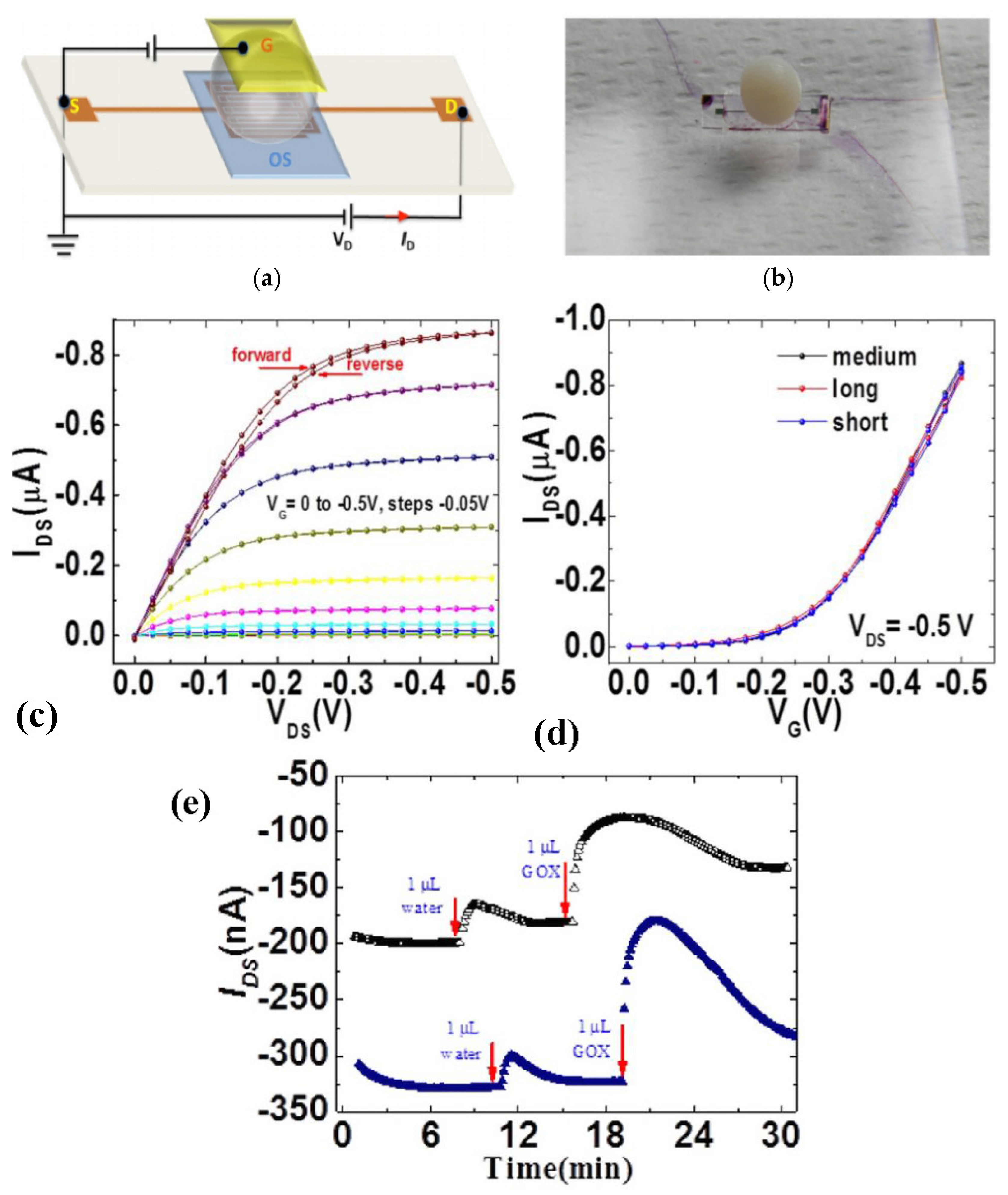
  74. Minamiki, T.; Minami, T.; Kurita, R.; Niwa, O.; Wakida, S.-I.; Fukuda, K.; Kumaki, D.; Tokito, S. Accurate and reproducible detection of proteins in water using an extended-gate type organic transistor biosensor. Appl. Phys. Lett. 2014, 104, 243703. [Google Scholar] [CrossRef]
  75. Dumitru, L.M.; Manoli, K.; Magliulo, M.; Palazzo, G.; Torsi, L. Low-voltage solid electrolyte-gated ofets for gas sensing applications. Microelectron. J. 2014, 45, 1679–1683. [Google Scholar] [CrossRef]
  76. Mulla, M.; Seshadri, P.; Torsi, L.; Manoli, K.; Mallardi, A.; Ditaranto, N.; Santacroce, M.; Di Franco, C.; Scamarcio, G.; Magliulo, M. Uv crosslinked poly (acrylic acid): A simple method to bio-functionalize electrolyte-gated ofet biosensors. J. Mater. Chem. B 2015, 3, 5049–5057. [Google Scholar] [CrossRef]
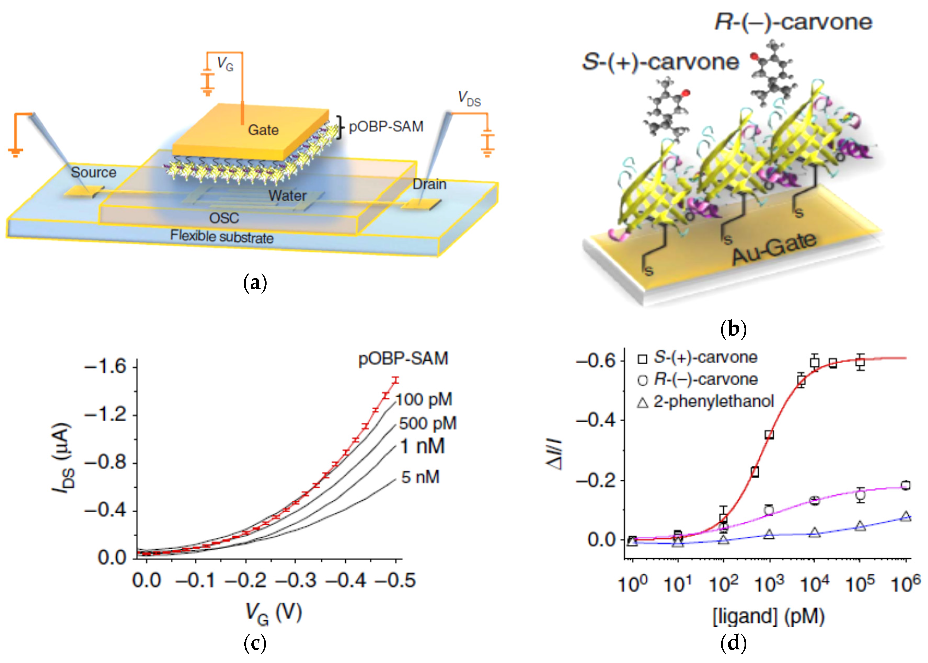
  77. Mulla, M.Y.; Tuccori, E.; Magliulo, M.; Lattanzi, G.; Palazzo, G.; Persaud, K.; Torsi, L. Capacitance-modulated transistor detects odorant binding protein chiral interactions. Nat. Commun. 2015, 6. [Google Scholar] [CrossRef] [PubMed]
  78. Kline, R.J.; McGehee, M.D.; Kadnikova, E.N.; Liu, J.; Frechet, J.M. Controlling the field-effect mobility of regioregular polythiophene by changing the molecular weight. Adv. Mater. 2003, 15, 1519–1522. [Google Scholar] [CrossRef]
  79. Chang, J.-F.; Sun, B.; Breiby, D.W.; Nielsen, M.M.; Sölling, T.I.; Giles, M.; McCulloch, I.; Sirringhaus, H. Enhanced mobility of poly (3-hexylthiophene) transistors by spin-coating from high-boiling-point solvents. Chem. Mater. 2004, 16, 4772–4776. [Google Scholar] [CrossRef] [Green Version]
  80. Heffner, G.W.; Pearson, D.S. Molecular characterization of poly (3-hexylthiophene). Macromolecules 1991, 24, 6295–6299. [Google Scholar] [CrossRef]
  81. Bao, Z.; Dodabalapur, A.; Lovinger, A.J. Soluble and processable regioregular poly (3-hexylthiophene) for thin film field-effect transistor applications with high mobility. Appl. Phys. Lett. 1996, 69, 4108–4110. [Google Scholar] [CrossRef]
  82. Sirringhaus, H.; Tessler, N.; Friend, R.H. Integrated optoelectronic devices based on conjugated polymers. Science 1998, 280, 1741–1744. [Google Scholar] [CrossRef] [PubMed]
  83. Hugger, S.; Thomann, R.; Heinzel, T.; Thurn-Albrecht, T. Semicrystalline morphology in thin films of poly (3-hexylthiophene). Colloid Polym. Sci. 2004, 282, 932–938. [Google Scholar]
  84. Cho, S.; Lee, K.; Yuen, J.; Wang, G.; Moses, D.; Heeger, A.J.; Surin, M.; Lazzaroni, R. Thermal annealing-induced enhancement of the field-effect mobility of regioregular poly (3-hexylthiophene) films. J. Appl. Phys. 2006, 100, 114503. [Google Scholar] [CrossRef]
  85. Gurau, M.C.; Delongchamp, D.M.; Vogel, B.M.; Lin, E.K.; Fischer, D.A.; Sambasivan, S.; Richter, L.J. Measuring molecular order in poly (3-alkylthiophene) thin films with polarizing spectroscopies. Langmuir 2007, 23, 834–842. [Google Scholar] [CrossRef] [PubMed]
  86. Alexiadis, O.; Mavrantzas, V.G. All-atom molecular dynamics simulation of temperature effects on the structural, thermodynamic, and packing properties of the pure amorphous and pure crystalline phases of regioregular p3ht. Macromolecules 2013, 46, 2450–2467. [Google Scholar] [CrossRef]
  87. Mårdalen, J.; Samuelsen, E.J.; Gautun, O.R.; Carlsen, P.H. Chain configuration of poly (3-hexylthiophene) as revealed by detailed x-ray diffraction studies. Solid State Commun. 1991, 77, 337–339. [Google Scholar] [CrossRef]
  88. Prosa, T.; Winokur, M.; Moulton, J.; Smith, P.; Heeger, A. X-ray structural studies of poly (3-alkylthiophenes): An example of an inverse comb. Macromolecules 1992, 25, 4364–4372. [Google Scholar] [CrossRef]
  89. Marchant, S.; Foot, P. Annealing behaviour of conductive poly (3-hexylthiophene) films. Polymer 1997, 38, 1749–1751. [Google Scholar] [CrossRef]
  90. Favia, P.; Sardella, E.; Gristina, R.; d’Agostino, R. Novel plasma processes for biomaterials: Micro-scale patterning of biomedical polymers. Surf. Coat. Technol. 2003, 169, 707–711. [Google Scholar] [CrossRef]
  91. Kergoat, L.; Battaglini, N.; Miozzo, L.; Piro, B.; Pham, M.-C.; Yassar, A.; Horowitz, G. Use of poly (3-hexylthiophene)/poly (methyl methacrylate)(p3ht/pmma) blends to improve the performance of water-gated organic field-effect transistors. Org. Electron. 2011, 12, 1253–1257. [Google Scholar] [CrossRef] [Green Version]
  92. Toss, H.; Suspene, C.; Piro, B.; Yassar, A.; Crispin, X.; Kergoat, L.; Pham, M.-C.; Berggren, M. On the mode of operation in electrolyte-gated thin film transistors based on different substituted polythiophenes. Org. Electron. 2014, 15, 2420–2427. [Google Scholar] [CrossRef]
  93. Suspène, C.; Piro, B.; Reisberg, S.; Pham, M.-C.; Toss, H.; Berggren, M.; Yassar, A.; Horowitz, G. Copolythiophene-based water-gated organic field-effect transistors for biosensing. J. Mater. Chem. B 2013, 1, 2090–2097. [Google Scholar] [CrossRef]
  94. Chabinyc, M.L.; Endicott, F.; Vogt, B.D.; DeLongchamp, D.M.; Lin, E.K.; Wu, Y.; Liu, P.; Ong, B.S. Effects of humidity on unencapsulated poly (thiophene) thin-film transistors. Appl. Phys. Lett. 2006, 88, 113514. [Google Scholar] [CrossRef]
  95. Hoshino, S.; Yoshida, M.; Uemura, S.; Kodzasa, T.; Takada, N.; Kamata, T.; Yase, K. Influence of moisture on device characteristics of polythiophene-based field-effect transistors. J. Appl. Phys. 2004, 95, 5088–5093. [Google Scholar] [CrossRef]
  96. Caronna, T.; Forte, M.; Catellani, M.; Meille, S.V. Photodegradation and photostabilization studies of poly (3-butylthiophene) in the solid state. Chem. Mater. 1997, 9, 991–995. [Google Scholar] [CrossRef]
  97. Manoli, K.; Dumitru, L.M.; Mulla, M.Y.; Magliulo, M.; Franco, C.D.; Santacroce, M.V.; Scamarcio, G.; Torsi, L. A comparative study of the gas sensing behavior in p3ht-and pbttt-based otfts: The influence of film morphology and contact electrode position. Sensors 2014, 14, 16869–16880. [Google Scholar] [CrossRef] [PubMed]
  98. Do, K.; Huang, D.M.; Faller, R.; Moulé, A.J. A comparative md study of the local structure of polymer semiconductors p3ht and pbttt. Phys. Chem. Chem. Phys. 2010, 12, 14735–14739. [Google Scholar] [CrossRef] [PubMed]
  99. Porrazzo, R.; Bellani, S.; Luzio, A.; Lanzarini, E.; Caironi, M.; Antognazza, M.R. Improving mobility and electrochemical stability of a water-gated polymer field-effect transistor. Org. Electron. 2014, 15, 2126–2134. [Google Scholar] [CrossRef]
  100. Al Naim, A.F.; Grell, M. Organic solvents as gate media for thin-film transistors. J. Appl. Phys. 2012, 112, 114502. [Google Scholar] [CrossRef]
  101. Cho, E.; Risko, C.; Kim, D.; Gysel, R.; Cates Miller, N.; Breiby, D.W.; McGehee, M.D.; Toney, M.F.; Kline, R.J.; Bredas, J.-L. Three-dimensional packing structure and electronic properties of biaxially oriented poly (2, 5-bis (3-alkylthiophene-2-yl) thieno [3, 2-b] thiophene) films. J. Am. Chem. Soc. 2012, 134, 6177–6190. [Google Scholar] [CrossRef] [PubMed]
  102. McCulloch, I.; Heeney, M.; Bailey, C.; Genevicius, K.; MacDonald, I.; Shkunov, M.; Sparrowe, D.; Tierney, S.; Wagner, R.; Zhang, W. Liquid-crystalline semiconducting polymers with high charge-carrier mobility. Nat. Mater. 2006, 5, 328–333. [Google Scholar] [CrossRef] [PubMed]
  103. Tsao, H.N.; Müllen, K. Improving polymer transistor performance via morphology control. Chem. Soc. Rev. 2010, 39, 2372–2386. [Google Scholar] [CrossRef] [PubMed]
  104. Schmoltner, K.; Kofler, J.; Klug, A.; List-Kratochvil, E. Electrolyte-gated organic field-effect transistors for sensing in aqueous media. SPIE Proc. 2013. [Google Scholar] [CrossRef]
  105. Casalini, S.; Dumitru, A.C.; Leonardi, F.; Bortolotti, C.A.; Herruzo, E.T.; Campana, A.; de Oliveira, R.F.; Cramer, T.; Garcia, R.; Biscarini, F. Multiscale sensing of antibody-antigen interactions by organic transistors and single-molecule force spectroscopy. ACS Nano 2015, 9, 5051–5062. [Google Scholar] [CrossRef] [PubMed]
  106. Lee, C.-Y.; Hwang, J.-C.; Chueh, Y.-L.; Chang, T.-H.; Cheng, Y.-Y.; Lyu, P.-C. Hydrated bovine serum albumin as the gate dielectric material for organic field-effect transistors. Org. Electron. 2013, 14, 2645–2651. [Google Scholar] [CrossRef]
  107. Dumitru, L.; Manoli, K.; Magliulo, M.; Ligonzo, T.; Palazzo, G.; Torsi, L. A hydrogel capsule as gate dielectric in flexible organic field-effect transistors. APL Mater. 2015, 3, 014904. [Google Scholar] [CrossRef]
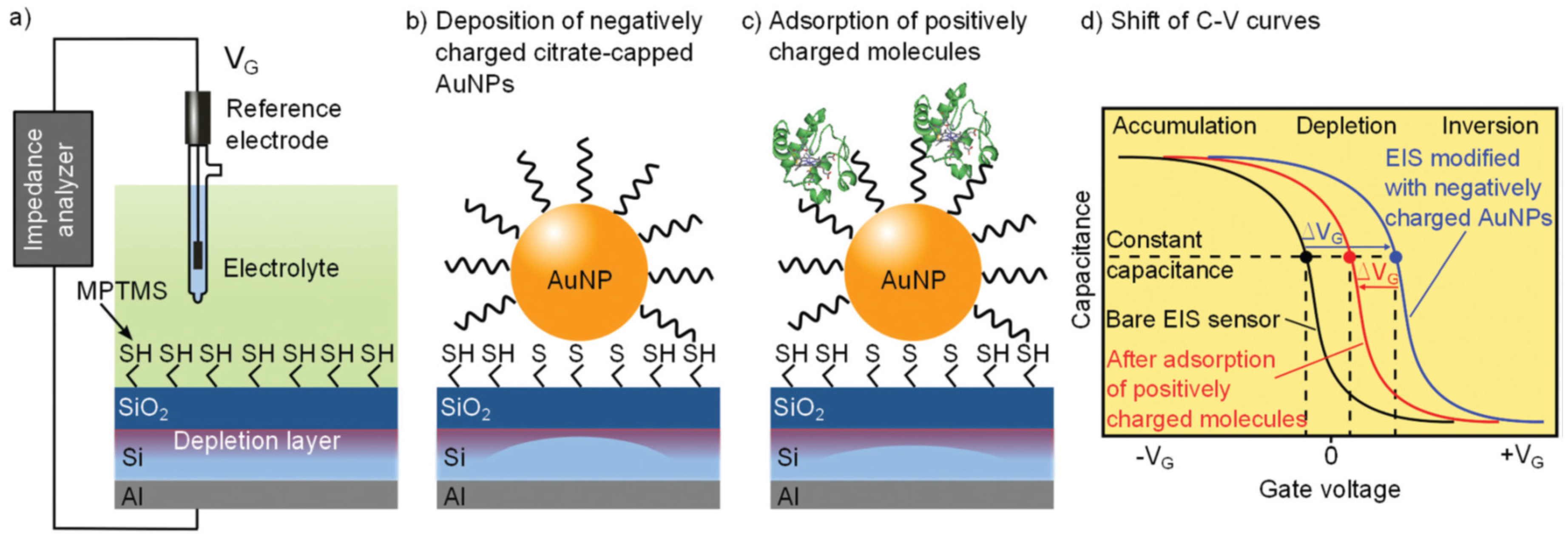
  108. Poghossian, A.; Bäcker, M.; Mayer, D.; Schöning, M.J. Gating capacitive field-effect sensors by the charge of nanoparticle/molecule hybrids. Nanoscale 2015, 7, 1023–1031. [Google Scholar] [CrossRef] [PubMed]
  109. Hammock, M.L.; Knopfmacher, O.; Naab, B.D.; Tok, J.B.H.; Bao, Z. Investigation of Protein Detection Parameters Using Nanofunctionalized Organic Field-Effect Transistors. ACS Nano 2013, 7, 3970–3980. [Google Scholar] [CrossRef] [PubMed]
Figure 1. General scheme of an organic field-effect transistor (OFET) (a) and an electrolyte-gated organic field-effect transistor (EGOFET) (b). Adapted from [8] with kind permission from Springer Science+Business Media. © Springer-Verlag, 2011.
Electronics 05 00009 g001
Figure 2. Illustration of the compact and diffuse layers corresponding to OFET and EGOFET, respectively. Adapted from [8] with kind permission from Springer Science+Business Media. © Springer-Verlag, 2011.
Electronics 05 00009 g002aElectronics 05 00009 g002b
Figure 3. Scheme of the first water-gated EGOFET. The semiconductor was rubrene and the gate a platinum wire. Reproduced from [10]. Copyright © 2010, WILEY-VCH Verlag GmbH & Co. KGaA, Weinheim.
Electronics 05 00009 g003
Figure 4. Most reported semiconducting oligomers and polymers in EGOFET biosensors.
Electronics 05 00009 g004
Figure 5. Lamelar structure of poly(3-hexylthiophène) (P3HT), normal or parallel to the substrate, respectively. Reprinted from [54] by permission from Macmillan Publishers Ltd. copyright, 1999.
Electronics 05 00009 g005
Figure 6. SEM image of (a) P3HT and (b) pBTTT crystalline structure. Reproduced from [97]. Creative Commons Attribution License (CC BY).
Electronics 05 00009 g006
Figure 7. (a) Schematic drawing of the transistor architecture and the different functionalizations investigated. (b) Transfer curves of untreated, oxidized and APTES-functionalized transistors, measured at pH 5. (c) Threshold voltage shift of untreated, APTES-functionalized and UV-oxidized α6T as a function of pH. (d) ID versus time, during a penicillin titration in PBS buffer. The green line corresponds to the response of a device functionalized with APTES and penicillinase, while the grey line depicts the ID response of an untreated α6T. Adapted from [11]. Copyright © 2012, WILEY-VCH Verlag GmbH & Co. KGaA, Weinheim.
Electronics 05 00009 g007
Figure 8. (A) Schematic view of the EGOFET device. (B) Transfer characteristics after (a) immobilization of ODN probes and (b) a blank sample after soaking in a bath similar to (a) but without ODN. Transfer curves for hybridization with (c) a complementary target and (d) a random target. Transfer curves for (e) a complementary target and (f) a random target in water instead of PBS. Adapted from [70] with permission from Elsevier. Copyright © 2011, Elsevier B.V. All rights reserved.
Electronics 05 00009 g008
Figure 9. (A) Chemical structure of P3HT, used as organic semiconductor. (B) Schematic view of an electrolyte gated organic field-effect transistor with the pdEthAA coating deposited by PE-CVD on the P3HT layer. Reproduced from [71]. Copyright © 2012, WILEY-VCH Verlag GmbH & Co. KGaA, Weinheim.
Electronics 05 00009 g009
Figure 10. IDS–VDS curves of EGOFET devices fabricated with (a) pristine P3HT and pdEthAA/ P3HT bilayer deposited by PE-CVD for: (b) 15 s; (c) 5 s; and (d) 3 s. L = 2 μm and W = 10,000 μm. Reproduced from [71]. Copyright © 2012, WILEY-VCH Verlag GmbH & Co. KGaA, Weinheim.
Electronics 05 00009 g010
Figure 11. (A) Structure of P3HT:P3HT-COOH:P3HT-biotin terpolymer. (B) Transfer curves at saturation for P3HT:P3HT-COOH:P3HT-biotin based transistors treated with 1-octanol before and after incubation with proteins. Reproduced from [93] with permission from The Royal Society of Chemistry.
Electronics 05 00009 g011aElectronics 05 00009 g011b
Figure 12. (A) Schematic view with different thicknesses of the bioreceptor layer. (B) Effect of the ionic strength on the fractional changes of the (a,b) current and (c,d) capacitance for a phospholipid/streptavidin/antibody (PL/SA/Ab) (a,c) and PL/SA/Ab/CRP (b,d) multilayers. Reproduced from [30]. © 2014, WILEY-VCH Verlag GmbH & Co. KGaA, Weinheim.
Electronics 05 00009 g012aElectronics 05 00009 g012b
Figure 13. (a) Transfer characteristics of the biotin-functionalized phospholipid bilayer-EGOFET in PBS, pH 7.4 (open symbols) and streptavidin (full symbols) solutions. (b,c) Diagram for the rationale leading to the IDS current increase. Reproduced from [64]. Copyright © 2013, WILEY-VCH Verlag GmbH & Co. KGaA, Weinheim.
Electronics 05 00009 g013
Figure 14. (A) Schematic illustration of the fabrication process of an EGOFET biosensor: (a) after deposition of pBTTT on the substrate; (b) poly(acrylic acid) coating spin-coated and cross-linked; (c) biotinylated phospholipids anchored on the PAA coating; and (d) EGOFET configuration comprising a gold gate electrode and a droplet of PBS as dielectric. (B) (a) IDS–VG transfer curves in PBS, pH 7.4 (line), and streptavidin solutions at concentrations of 0.16 nM (circles) and 1.6 μM (triangles) in PBS; and (b) relative response of the EGOFET as a function of the streptavidin concentration. Reproduced from [76] with permission from the Royal Society of Chemistry.
Electronics 05 00009 g014
Figure 15. (A) Schematic illustration of the gate-modified EGOFET, and of the AFM measurements. (B) I-V transfer characteristics for (a) HSC6NH2- and (b) Protein G-based protocols. Normalized mobility ratio (c) and threshold voltage (d) trends corresponding to the stepwise functionalization. Adapted with permission from [105]. Copyright © 2015, American Chemical Society.
Electronics 05 00009 g015
Figure 16. EGOFET where the gate is modified by a SAM of odorant binding protein (pOBP-SAM). (a) Schematic structure. The OSC is pBTTT-C14. (b) pOBP protein structure and interaction with the odorant molecule. (c) IDS–VG transfer characteristics reported as a function to concentrations of the odorant molecule (carvone). (d) Calibration curves for the (R)-(−)- and (S)-(+)-carvone and for a non-specific molecule. Reproduced from [77] under Creative Commons Attribution license.
Electronics 05 00009 g016
Figure 17. Schematic illustration (a) and picture (b) of the alginate-gated OFET; output characteristics (c) and transfer curves (d); and (e) IDS changes versus time, for injection of water (blank) and glucose. Reproduced from [107] under Creative Commons Attribution 3.0 Unported license.
Electronics 05 00009 g017
Figure 18. Schematic of (a) a capacitive Al/p-Si/SiO2 sensor after silanization; (b) deposition of negatively charged citrate-capped AuNPs (b); and (c) adsorption of positively charged molecules on the AuNPs. (d) Capacitance vs. gate voltage curves. Reproduced from [108] with permission from the Royal Society of Chemistry.
Electronics 05 00009 g018
Table 1. Influence of probe grafting and target hybridization on device performance with phosphate buffer saline (PBS) as electrolyte, and influence of probe hybridization with water as electrolyte. Adapted from [70] with permission from Elsevier. Copyright © 2011, Elsevier B.V. All rights reserved.
ODN grafting (Figure 8a,b)
ODN probe∆VG min / VIoff (bare film) / Ioff (probe-modified film)
Yes−0.31 ± 0.05 11.1 ± 3.7
No+0.16 ± 0.050.5 ± 0.12
DNA hybrid. in PBS (Figure 8c,d)
ODN target∆VG min / VIoff (probe-modified film) / Ioff (hybridization)
HIV−0.06 ± 0.021.7 ± 0.45
RAND−0.03 ± 0.031.3 ± 0.28
DNA hybrid. in H2O (Figure 8e,f)
ODN probe∆VGmin / VIoff (probe-modified film) / Ioff (hybridization)
HIV−0.03 ± 0.023.4 ± 1.5
RAND−0.04 ± 0.071.04 ± 0.04

