
Optical Orientation and Inverse Spin Hall Effect as Effective Tools to Investigate Spin-Dependent Diffusion

 ,
, 
Abstract
:1. Introduction
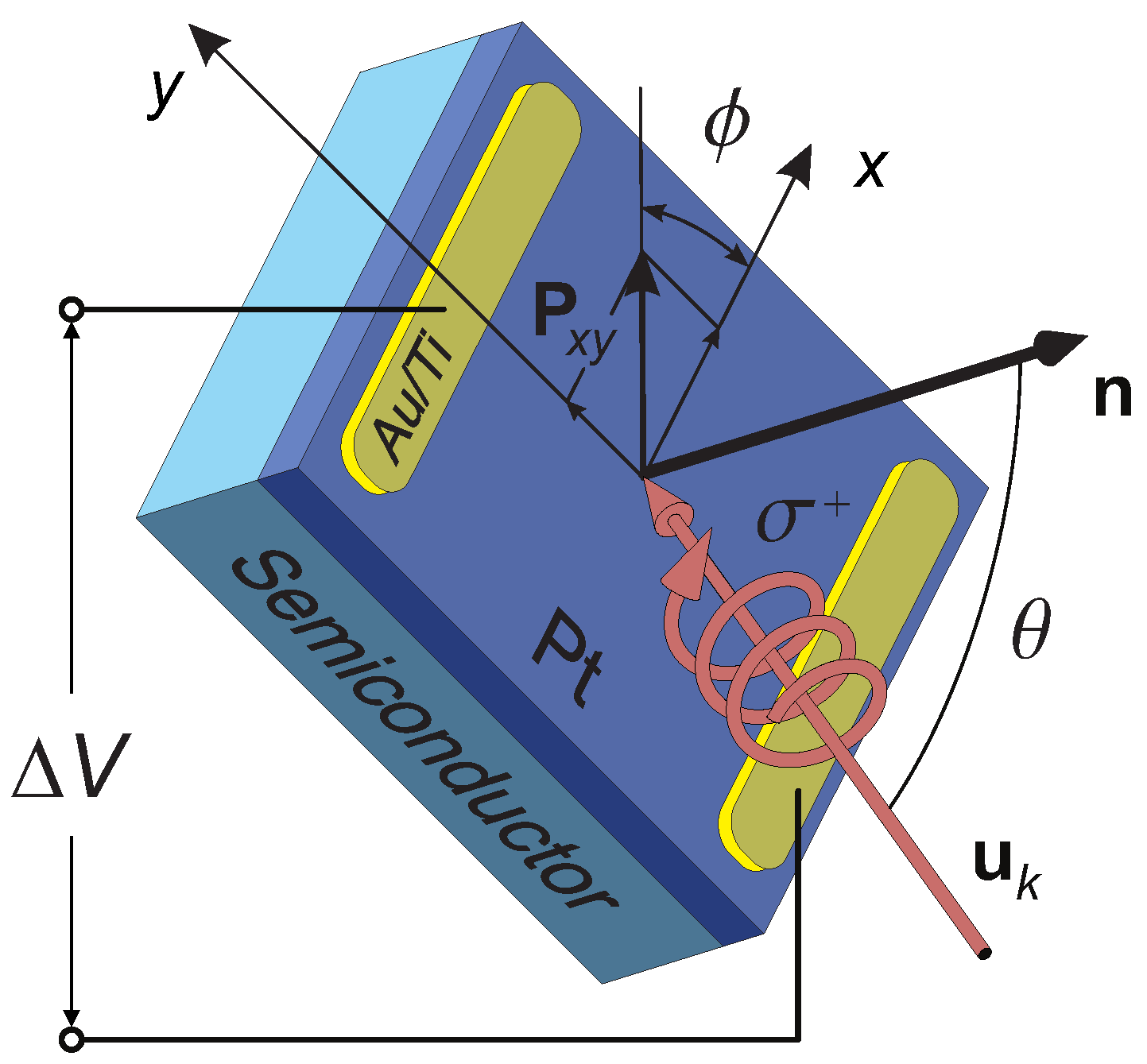
2. Experimental
3. Results and Discussion
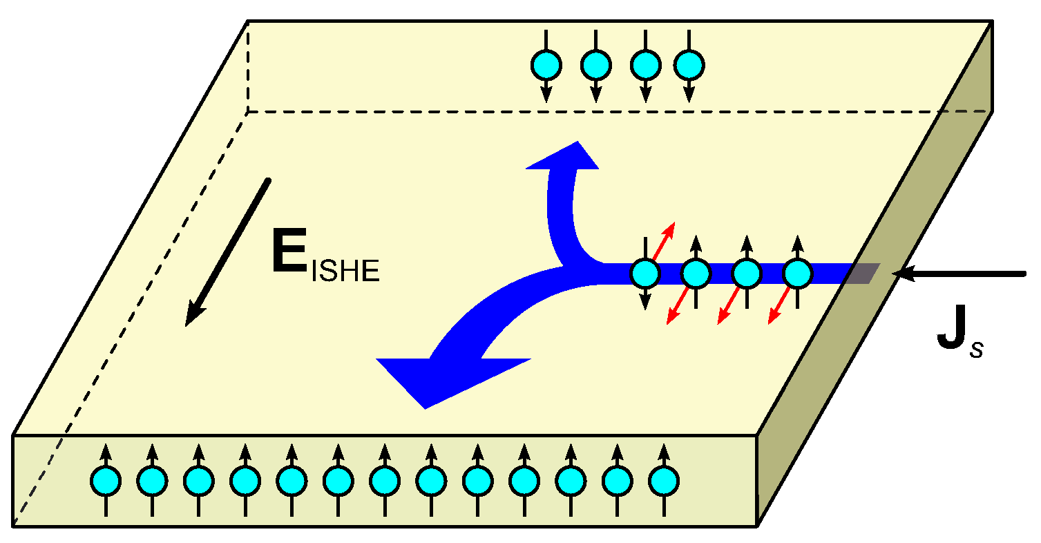
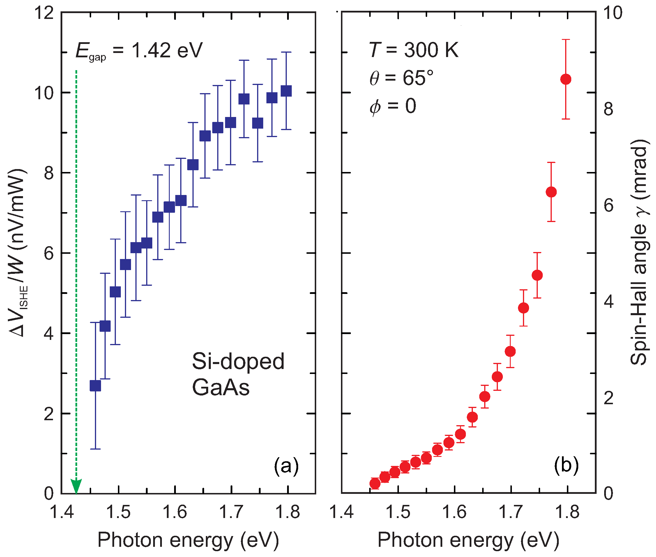
3.1. Extrinsic spin-Hall Conductivity in Si-doped GaAs
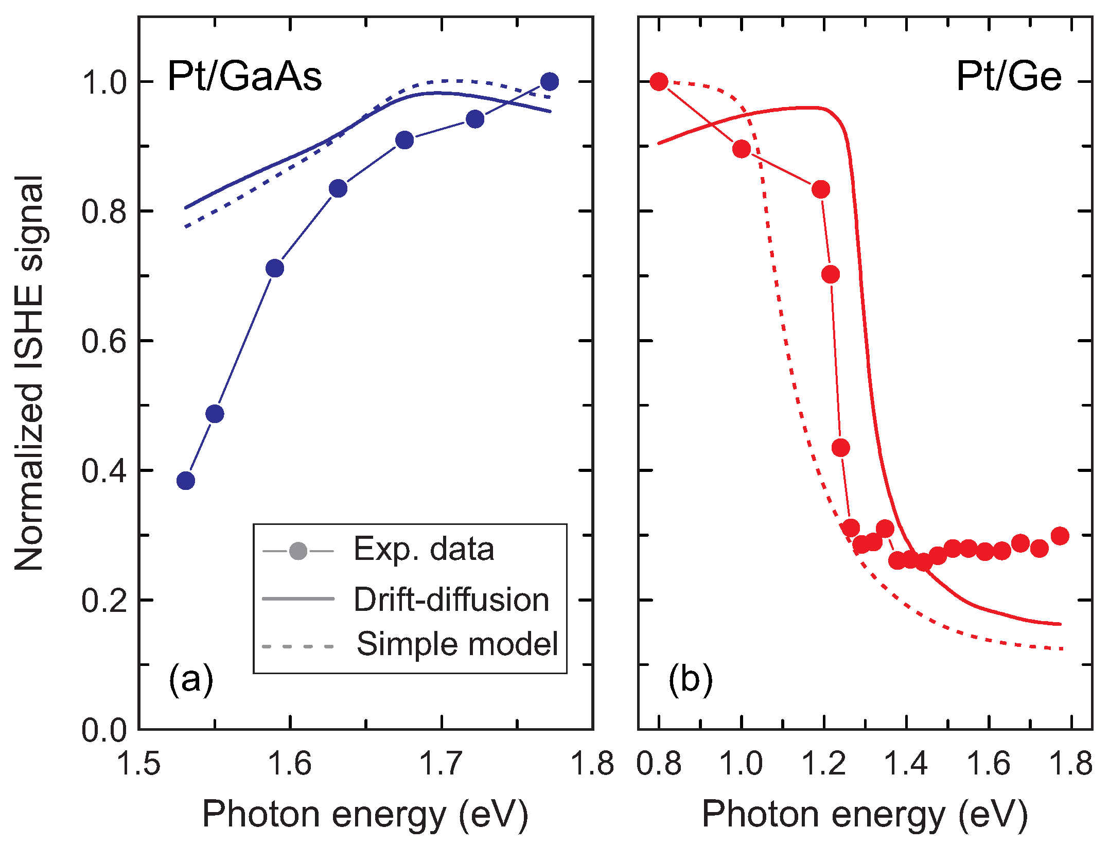
3.2. Photon Energy Dependence of the Optically-Induced Inverse spin-Hall Effect in Pt/GaAs and Pt/Ge
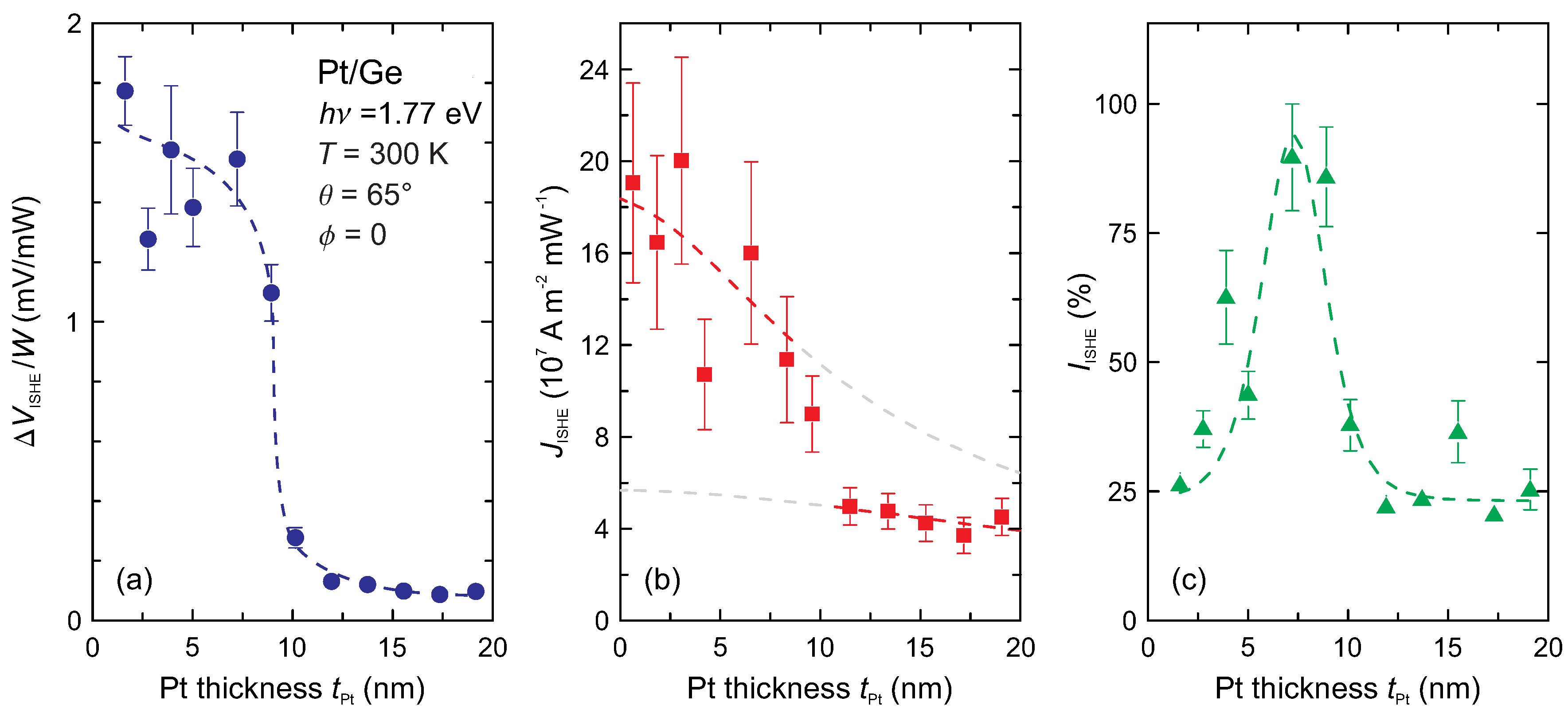
3.3. Pt Thickness Dependence of the Optically-Induced Inverse spin-Hall Effect in Pt/Ge
4. Discussion
5. Conclusions
Acknowledgments
Author Contributions
Conflicts of Interest
Abbreviations
| HH | Heavy hole |
| ISHE | Inverse spin Hall effect |
| LH | Light hole |
| MTJ | Magnetic tunnel junction |
| SHE | Spin Hall effect |
| SO | Split-off |
References
- Žutić, I.; Fabian, J.; Das Sarma, S. Spintronics: Fundamentals and applications. Rev. Mod. Phys. 2004, 76, 323–410. [Google Scholar] [CrossRef]
- Tserkovnyak, Y.; Brataas, A.; Bauer, G.E.W. Enhanced Gilbert Damping in Thin Ferromagnetic Films. Phys. Rev. Lett. 2002, 88, 117601. [Google Scholar] [CrossRef] [PubMed]
- Tserkovnyak, Y.; Brataas, A.; Bauer, G.E.W.; Halperin, B.I. Nonlocal magnetization dynamics in ferromagnetic heterostructures. Rev. Mod. Phys. 2005, 77, 1375–1421. [Google Scholar] [CrossRef]
- Johnson, M.; Silsbee, R.H. Coupling of electronic charge and spin at a ferromagnetic-paramagnetic metal interface. Phys. Rev. B 1998, 37, 5312–5325. [Google Scholar] [CrossRef]
- Rashba, E.I. Theory of electrical spin injection: Tunnel contacts as a solution of the conductivity mismatch problem. Phys. Rev. B 2000, 62, R16267–R16270. [Google Scholar] [CrossRef]
- Fert, A.; Jaffrès, H. Conditions for efficient spin injection from a ferromagnetic metal into a semiconductor. Phys. Rev. B 2001, 64, 184420. [Google Scholar] [CrossRef]
- Lampel, G. Nuclear dynamic polarization by optical electronic saturation and optical pumping in semiconductors. Phys. Rev. Lett. 1968, 20, 491–493. [Google Scholar] [CrossRef]
- Meier, F.; Zakharchenya, B.P. Optical Orientation. Mod. Probl. Condens. Matter Sci. 1984, 8, 1–523. [Google Scholar]
- Pierce, D.; Meier, F. Photoemission of spin-polarized electrons from GaAs. Phys. Rev. B 1976, 13, 5484–5500. [Google Scholar] [CrossRef]
- Allenspach, R.; Meier, F.; Pescia, D. Experimental Symmetry Analysis of Electronic States by Spin-Dependent Photoemission. Phys. Rev. Lett. 1983, 51, 2148–2150. [Google Scholar] [CrossRef]
- Bottegoni, F.; Isella, G.; Cecchi, S.; Ciccacci, F. Spin polarized photoemission from strained Ge epilayers. Appl. Phys. Lett. 2011, 98, 242107. [Google Scholar] [CrossRef]
- Bottegoni, F.; Ferrari, F.; Isella, G.; Finazzi, M.; Ciccacci, F. Enhanced orbital mixing in the valence band of strained germanium. Phys. Rev. B 2012, 85, 245312. [Google Scholar] [CrossRef]
- Ferrari, A.; Bottegoni, F.; Isella, G.; Cecchi, S.; Ciccacci, F. Epitaxial Si1−xGex alloys studied by spin-polarized photoemission. Phys. Rev. B 2013, 88, 115209. [Google Scholar] [CrossRef]
- Dal Conte, S.; Bottegoni, F.; Pogna, E.A.A.; De Fazio, D.; Ambrogio, S.; Bargigia, I.; D’Andrea, C.; Lombardo, A.; Bruna, M.; Ciccacci, F.; et al. Ultrafast valley relaxation dynamics in monolayer MoS2 probed by nonequilibrium optical techniques. Phys. Rev. B 2015, 92, 235425. [Google Scholar] [CrossRef]
- Bottegoni, F.; Celebrano, M.; Bollani, M.; Biagioni, P.; Isella, G.; Ciccacci, F.; Finazzi, M. Spin voltage generation through optical excitation of complementary spin populations. Nat. Mater. 2014, 13, 790–795. [Google Scholar] [CrossRef] [PubMed]
- Kikkawa, J.M.; Awschalom, D.D. Resonant Spin Amplification in n-Type GaAs. Phys. Rev. Lett. 1998, 80, 4313–4316. [Google Scholar] [CrossRef]
- Pezzoli, F.; Bottegoni, F.; Trivedi, D.; Ciccacci, F.; Giorgioni, A.; Li, P.; Cecchi, S.; Grilli, E.; Song, Y.; Guzzi, M.; et al. Optical Spin Injection and Spin Lifetime in Ge Heterostructures. Phys. Rev. Lett. 2012, 108, 156603. [Google Scholar] [CrossRef] [PubMed]
- Hilton, D.J.; Tang, C.L. Optical Orientation and Femtosecond Relaxation of Spin-Polarized Holes in GaAs. Phys. Rev. Lett. 2002, 89, 146601. [Google Scholar] [CrossRef] [PubMed]
- Loren, E.J.; Rioux, J.; Lange, C.; Sipe, J.E.; van Driel, H.M.; Smirl, A.L. Hole spin relaxation and intervalley electron scattering in germanium. Phys. Rev. B 2011, 84, 214307. [Google Scholar] [CrossRef]
- D’yakonov, M.I.; Perel’, V.I. Spin relaxation of conduction electrons in noncentrosymmetric semiconductors. Sov. Phys. Solid State 1972, 13, 3023–3026. [Google Scholar]
- Bottegoni, F.; Drouhin, H.-J.; Fishman, G.; Wegrowe, J.-E. Probability- and spin-current operators for effective Hamiltonians. Phys. Rev. B 2012, 85, 235313. [Google Scholar] [CrossRef]
- Bottegoni, F.; Drouhin, H.-J.; Wegrowe, J.-E.; Fishman, G. Probability-current definition in presence of spin-orbit interaction. J. App. Phys. 2012, 111, 07C305. [Google Scholar] [CrossRef]
- Allenspach, R.; Meier, F.; Pescia, D. Spin polarized photoemission from GaAs and Ge: Temperature dependence of the threshold polarization. Appl. Phys. Lett. 1984, 44, 1107–1109. [Google Scholar] [CrossRef]
- Parsons, R.R. Band-To-Band Optical Pumping in Solids and Polarized Photoluminescence. Phys. Rev. Lett. 1969, 23, 1152–1154. [Google Scholar] [CrossRef]
- Pezzoli, F.; Qing, L.; Giorgioni, A.; Isella, G.; Grilli, E.; Guzzi, M.; Dery, H. Spin and energy relaxation in germanium studied by spin-polarized direct-gap photoluminescence. Phys. Rev. B 2013, 88, 045204. [Google Scholar] [CrossRef]
- Jullière, M. Tunneling between ferromagnetic films. Phys. Lett. 1975, 54A, 225–226. [Google Scholar] [CrossRef]
- D’yakonov, M.I.; Perel’, V.I. Possibility of Orienting Electron Spins with Current. JETP Lett. 1971, 13, 467–469. [Google Scholar]
- Saitoh, E.; Ueda, M.; Miyajima, H.; Tatara, G. Conversion of spin current into charge current at room temperature: Inverse spin-Hall effect. Appl. Phys. Lett. 2006, 88, 182509. [Google Scholar] [CrossRef]
- Bakun, A.A.; Zakharchenya, B.P.; Rogachev, A.A.; Tkachuk, M.N.; Fleisher, V.G. Observation of a surface photocurrent caused by optical orientation of electrons in a semiconductor. JETP Lett. 1984, 40, 1293–1295. [Google Scholar]
- Bottegoni, F.; Ferrari, A.; Isella, G.; Finazzi, M.; Ciccacci, F. Experimental evaluation of the spin-Hall conductivity in Si-doped GaAs. Phys. Rev. B 2013, 88, 121201(R). [Google Scholar] [CrossRef]
- Ando, K.; Morikawa, M.; Trypiniotis, T.; Fujikawa, Y.; Barnes, C.H.W.; Saitoh, E. Photoinduced inverse spin-Hall effect: Conversion of light-polarization information into electric voltage. Appl. Phys. Lett. 2010, 96, 082502. [Google Scholar] [CrossRef]
- Bottegoni, F.; Ferrari, A.; Cecchi, S.; Finazzi, M.; Ciccacci, F.; Isella, G. Photoinduced inverse spin Hall effect in Pt/Ge(001) at room temperature. Appl. Phys. Lett. 2013, 102, 152411. [Google Scholar] [CrossRef]
- Ando, K.; Morikawa, M.; Trypiniotis, T.; Fujikawa, Y.; Barnes, C.H.W.; Saitoh, E. Direct conversion of light-polarization information into electric voltage using photoinduced inverse spin-Hall effect in Pt/GaAs hybrid structure: Spin photodetector. J. Appl. Phys. 2010, 107, 113902. [Google Scholar] [CrossRef]
- Kato, Y.K.; Myers, R.C.; Gossard, A.C.; Awschalom, D.D. Observation of the spin Hall effect in semiconductors. Science 2004, 5703, 1910–1913. [Google Scholar] [CrossRef] [PubMed]
- Kato, Y.K.; Myers, R.C.; Gossard, A.C.; Awschalom, D.D. Current-Induced Spin Polarization in Strained Semiconductors. Phys. Rev. Lett. 2004, 93, 5326–5335. [Google Scholar] [CrossRef] [PubMed]
- Wunderlich, J.; Kaestner, B.; Sinova, J.; Jungwirth, T. Experimental Observation of the Spin-Hall Effect in a Two-Dimensional Spin-Orbit Coupled Semiconductor System. Phys. Rev. Lett. 2005, 94, 047204. [Google Scholar] [CrossRef] [PubMed]
- Averkiev, N.S.; D’yakonov, M.I. Current due to the inhomogeneity of the spin orientation of electrons in a semiconductor. Sov. Phys.: Semicond. 1983, 17, 393. [Google Scholar]
- Mott, N.F. The Scattering of Fast Electrons by Atomic Nuclei. Proc. R. Soc. A-Math. Phys. Eng. Sci. 1929, 794, 425–442. [Google Scholar] [CrossRef]
- Chazalviel, J.-N. Spin-dependent Hall effect in semiconductors. Phys. Rev. B 1975, 11, 3918–3934. [Google Scholar] [CrossRef]
- Engel, H.-A.; Halperin, B.I.; Rashba, E. Theory of Spin Hall Conductivity in n-Doped GaAs. Phys. Rev. Lett. 2005, 95, 166605. [Google Scholar] [CrossRef] [PubMed]
- Berger, L. Side-Jump Mechanism for the Hall Effect of Ferromagnets. Phys. Rev. B 1970, 11, 4559–4566. [Google Scholar] [CrossRef]
- Matsuzaka, S.; Ohno, Y.; Ohno, H. Electron density dependence of the spin Hall effect in GaAs probed by scanning Kerr rotation microscopy. Phys. Rev. B 2009, 80, 241305. [Google Scholar] [CrossRef]
- Isella, G.; Bottegoni, F.; Ferrari, A.; Finazzi, M.; Ciccacci, F. Photon energy dependence of photo-induced inverse spin-Hall effect in Pt/GaAs and Pt/Ge. Appl. Phys. Lett. 2015, 106, 232402. [Google Scholar] [CrossRef]
- Khamari, S.K.; Dixit, V.K.; Oak, S.M. Numerical simulation of inverse spin Hall spectra in Pt/GaAs hybrid structure. J. Phys. D: Appl. Phys. 2011, 44, 265104. [Google Scholar] [CrossRef]
- Hilsum, C. Simple empirical relationship between mobility and carrier concentration. Electron. Lett. 1974, 10, 259–260. [Google Scholar] [CrossRef]
- Aspnes, D.E.; Studna, A.A. Dielectric functions and optical parameters of Si, Ge, GaP, GaAs, GaSb, InP, InAs, and InSb from 1.5 to 6.0 eV. Phys. Rev. B 1983, 27, 985–1009. [Google Scholar] [CrossRef]
- Nastos, F.; Rioux, J.; Strimas-Mackey, M.; Mendoza, B.S.; Sipe, J.E. Full band structure LDA and k·p calculations of optical spin-injection. Phys. Rev. B 2007, 76, 205113. [Google Scholar] [CrossRef]
- Rioux, J.; Sipe, J.E. Optical injection and control in germanium: Thirty-band k·p theory. Phys. Rev. B 2010, 81, 155215. [Google Scholar] [CrossRef]
- Shockley, W.; Read, W.T. Statistics of the Recombinations of Holes and Electrons. Phys. Rev. 1952, 87, 835–842. [Google Scholar] [CrossRef]
- Bottegoni, F.; Ferrari, A.; Rortais, F.; Vergnaud, C.; Marty, A.; Isella, G.; Finazzi, M.; Jamet, M.; Ciccacci, F. Spin diffusion in Pt as probed by optically generated spin currents. Phys. Rev. B 2015, 92, 214403. [Google Scholar] [CrossRef]
- Castel, V.; Vlietstra, N.; Ben Youssef, J.; van Wees, B.J. Platinum thickness dependence of the inverse spin-Hall voltage from spin pumping in a hybrid yttrium iron garnet/platinum system. Appl. Phys. Lett. 2012, 101, 132414. [Google Scholar] [CrossRef]
- Schmidt, G.; Ferrand, D.; Molenkamp, L.W.; Filip, A.T.; van Wees, B.J. Fundamental obstacle for electrical spin injection from a ferromagnetic metal into a diffusive semiconductor. Phys. Rev. B 2000, 62, R4790–R4793. [Google Scholar] [CrossRef]
- Khamari, S.K.; Porwal, S.; Dixit, V.K.; Sharma, T.K. Temperature dependence of the photo-induced inverse spin Hall effect in Au/InP hybrid structures. Appl. Phys. Lett. 2014, 104, 042102. [Google Scholar] [CrossRef]
- Oltscher, M.; Ciorga, M.; Utz, M.; Schuh, D.; Bougeard, D.; Weiss, D. Electrical Spin Injection into High Mobility 2D Systems. Phys. Rev. Lett. 2014, 113, 236602. [Google Scholar] [CrossRef] [PubMed]


© 2016 by the authors; licensee MDPI, Basel, Switzerland. This article is an open access article distributed under the terms and conditions of the Creative Commons Attribution (CC-BY) license (http://creativecommons.org/licenses/by/4.0/).
Share and Cite
Finazzi, M.; Bottegoni, F.; Zucchetti, C.; Bollani, M.; Ballabio, A.; Frigerio, J.; Rortais, F.; Vergnaud, C.; Marty, A.; Jamet, M.; et al. Optical Orientation and Inverse Spin Hall Effect as Effective Tools to Investigate Spin-Dependent Diffusion. Electronics 2016, 5, 80. https://doi.org/10.3390/electronics5040080
Finazzi M, Bottegoni F, Zucchetti C, Bollani M, Ballabio A, Frigerio J, Rortais F, Vergnaud C, Marty A, Jamet M, et al. Optical Orientation and Inverse Spin Hall Effect as Effective Tools to Investigate Spin-Dependent Diffusion. Electronics. 2016; 5(4):80. https://doi.org/10.3390/electronics5040080
Chicago/Turabian StyleFinazzi, Marco, Federico Bottegoni, Carlo Zucchetti, Monica Bollani, Andrea Ballabio, Jacopo Frigerio, Fabien Rortais, Céline Vergnaud, Alain Marty, Matthieu Jamet, and et al. 2016. "Optical Orientation and Inverse Spin Hall Effect as Effective Tools to Investigate Spin-Dependent Diffusion" Electronics 5, no. 4: 80. https://doi.org/10.3390/electronics5040080