
Guided Modes in a Double-Well Asymmetric Potential of a Graphene Waveguide

Engineering Product Development, Singapore University of Technology and Design, Singapore 487372, Singapore
*
Author to whom correspondence should be addressed.
Electronics 2016, 5(4), 87; https://doi.org/10.3390/electronics5040087
Submission received: 27 October 2016
/
Revised: 28 November 2016
/
Accepted: 1 December 2016
/
Published: 7 December 2016
(This article belongs to the Special Issue Two-Dimensional Electronics and Optoelectronics)
Abstract
:The analogy between the electron wave nature in graphene electronics and the electromagnetic waves in dielectrics has suggested a series of optical-like phenomena, which is of great importance for graphene-based electronic devices. In this paper, we propose an asymmetric double-well potential on graphene as an electronic waveguide to confine the graphene electrons. The guided modes in this graphene waveguide are investigated using a modified transfer matrix method. It is found that there are two types of guided modes. The first kind is confined in one well, which is similar to the asymmetric quantum well graphene waveguide. The second kind can appear in two potential wells with double-degeneracy. Characteristics of all the possible guide modes are presented.
1. Introduction
A two-dimensional layer of carbon atoms known as graphene [1] has been investigated widely both theoretically and experimentally. Graphene has a unique band structure for which the electron and hole bands meet at two inequivalent points in the Brillouin zone. At these Dirac points, the electrons behave like quasi-particles according to the massless Dirac equation, which leads to a linear dispersion relation. The analogy between the electron wave nature in graphene electronics and the electromagnetic waves in dielectrics has suggested a series of optical-like phenomena, such as the Goos–Hänchen effect [2,3], negative refraction [4], collimation [5], birefringence [6], and the Bragg reflection [7] reported in recent papers.
Another analogy is the graphene-based electron waveguides [8,9,10,11,12,13,14,15,16,17,18], which will be useful for various graphene-based devices, such as electronic fiber [19]. The crux of such an electronic waveguide is the confinement of Dirac fermions in graphene. There are many schemes to confine electrons in graphene, e.g., electric confinement [20,21], magnetic confinement [22] and strain-induced confinement [16,17,18]. By having a quantum well in graphene to confine massless Dirac fermions, the guided modes in graphene-based waveguides with quantum well structure induced by an external electrical field have been investigated in detail [8,9,10]. Experimentally, gate-controlled electron guiding in graphene by tuning the carrier type and its density using local electrostatic fields has been achieved [12]. However, the confinement of the quasi-particles is not strong enough due to the Klein tunneling.
Another effective way to confine the electrons in graphene is by applying a uniform magnetic field [22] and the characteristics of magnetic waveguides in graphene have also been studied [13,14]. Recently, the strain-induced graphene waveguides has also attracted much attention [16,17,18]. Contrary to the electric or magnetic waveguide in graphene, the strain-induced waveguide confines electrons without any external fields. It confines the quasi-particles with the pseudo-magnetic field [23], which arises from the applied mechanical strain. The bound states of the strain-induced waveguides are dependent on the valleys, which is different from the electric and magnetic waveguides (valley independent). Furthermore, smooth one-dimensional potential [15,24,25,26] and velocity barriers [27] have been proposed to confine the Dirac fermions in graphene. Electrons can also be guided in nano-structured graphene, such as graphene nano-ribbons [28] and antidot lattice [29]. Recently, Allen et al. demonstrated the confinement of electron waves in graphene with the use of superconducting interferometry in a graphene Josephson junction [30].
For a given graphene waveguide with quantum well structures, the dispersion equation for its guided modes is normally determined by applying the continuity of wave function at the interfaces of the quantum well. This method is easy for one quantum well structure, but not for multiple or more complicated quantum well structures, e.g., a double-well potential. In this paper, we will apply a transfer matrix method [31,32,33] to deduce the dispersion equation for guided modes in a double-well potential structure. From the calculation, we will present the characteristics of the guided modes in detail, and report its novel properties as compared to other graphene-based waveguides.
In the present work, we focus on the properties of guided modes in a double-well asymmetric potential that acts as a slab waveguide for electron waves (based on Dirac solution) in a form similar to that in integrated optics. However, it should be noted that the optical properties or optical waves in graphene have also been investigated [34,35,36,37,38,39,40,41]. This work shows an analogy between the electron wave nature in graphene electronics and the electromagnetic waves in dielectrics.
2. Guided Mode and Dispersion Equation for a Double-Well Potential
In the presence of an electrostatic potential V(x), electrons inside a monolayer graphene can be described by the Dirac-like equation:
where are the Pauli matrices, and m/s is the Fermi velocity. is a two-component pseudo-spinor wave function, and are the smooth enveloping functions for two triangular sublattices in graphene, which can be expressed as due to its translation invariance in the direction. In terms of , Equation (1) is written as
By using the transfer matrix method [31,32,33], we obtain a matrix M to connect the wave functions at the two boundaries at and :
where , , . By solving Equation (3), one can immediately obtain the dispersion equation of a graphene waveguide (see below).
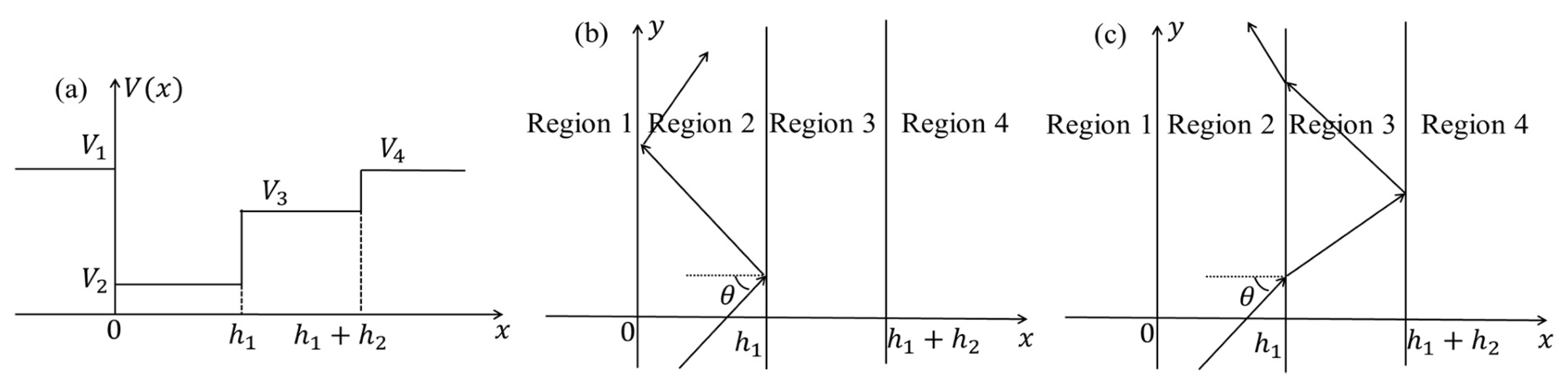
Here, we consider a double-well asymmetric potential for graphene waveguide as plotted in Figure 1a, where its potential distribution is denoted by
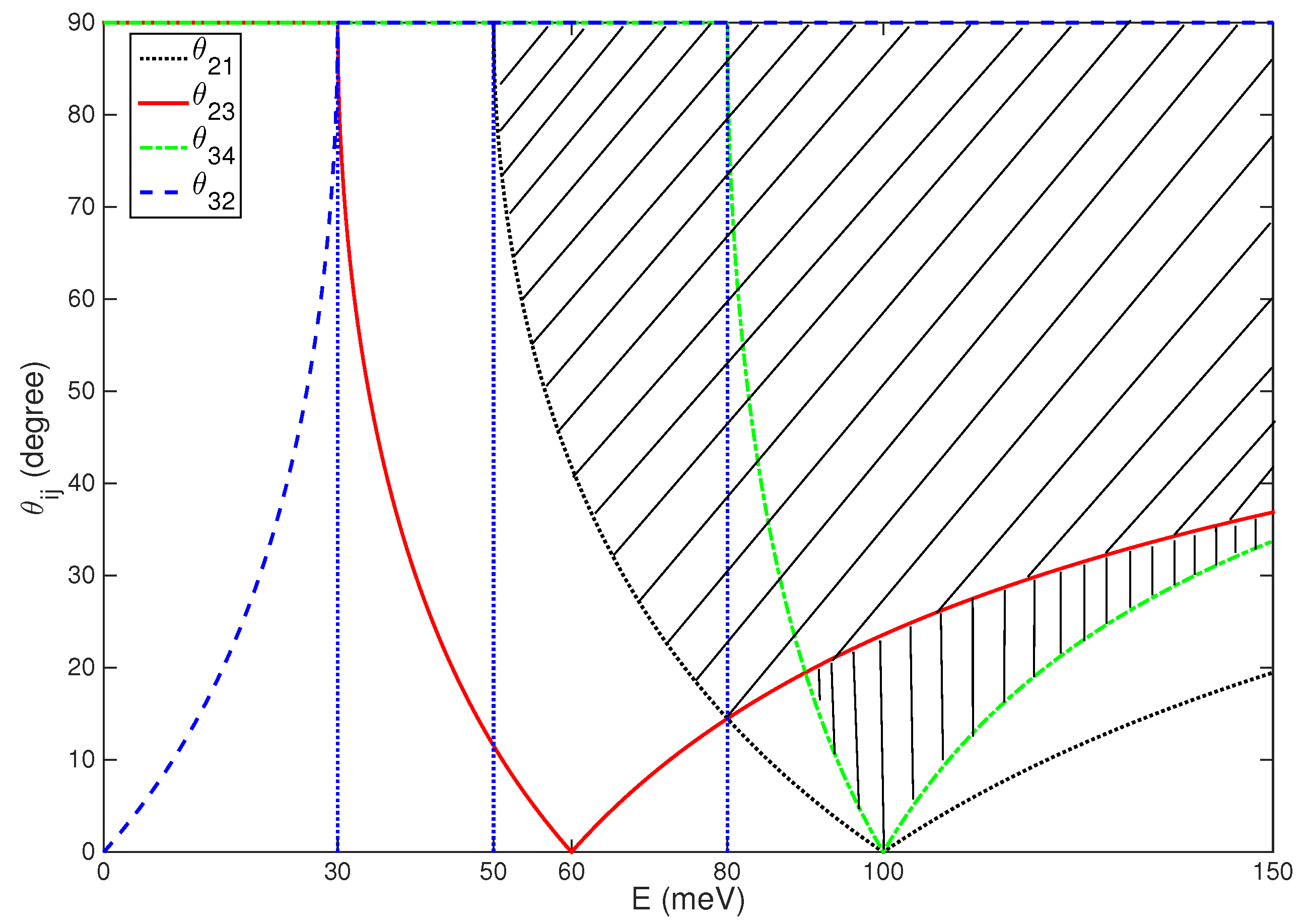
The proposed waveguide configuration can be realized by applying four gate-tunable potential barriers on single-layer graphene [42]. By tuning the applied voltage on the gate, a double-well asymmetric potential can be formed on graphene. For simplicity, we have unless it is specified elsewhere. In this model, we have neglected the microscopic details of the interaction effects such as the inter-valley coupling [43,44] and inter-valley scattering in the potential steps [44,45]. The electron wave incident into the quantum well (region 2) with an angle θ respect to the x-axis, and the guided modes are propagating in the y-direction. The critical angle of the incident electron waves from region i to region j is defined by
where , E is the energy of incident electron and is the electrostatic potential in the respective region . The critical angle is shown in Figure 2 as a function of the incidence energy E for , , , , and .
For a given guided mode, there will be total internal reflection of electron waves at both the two interfaces of a waveguide. For example, at large incidence angles , total reflection occurs in a specific range (marked with “slanted lines”) as plotted in Figure 2. In this range, the electron waves will be reflected at the interfaces back and forth with an angle of in region 2 () with a guided wave propagating in the axis as shown in Figure 1b.
For the angle within in region 2 and the angle in region 3, which lies in a range marked with “vertical lines” in Figure 2, the electron waves will refract into region 3, and total internal reflection occurs at the interface . The electron wave will oscillate in the region of as shown in Figure 1c. It is important to note that there are no guided modes within , as there is no angle θ to fulfill the condition . Thus, there are only two types of guided modes in a double-well potential. The first one is the guided modes in , and the other is the guided modes in .
To derive the dispersion equation, the electron wave function in the double-well potential can be written as:
Here, we have , , , , , . And , , , , , .
Based on the transfer matrix method, we have:
where , and .
By multiplying Equation (9) with matrix , we obtain
From Equation (10), we obtain the dispersion equation for the guided modes in a double-well potential, which is
and , , , , and . The dispersion equation for the guided modes obtained with the transfer matrix method is more convenient than the usual method that solving the Dirac equations from the continuity of wave function at the interfaces of quantum wells. The dispersion equation (Equation (11)) obtained for the double-well asymmetric potential can be recovered to that of the symmetric quantum well-based graphene waveguide by setting and . Thus, we have
which is the dispersion equation for a symmetric quantum well, as reported in Ref. [8]. Equation (12) can also be directly obtained by using the transfer matrix method:
3. Characteristics of the Guided Modes in a Double-Well Potential
For the guided mode in the region , the electron waves are evanescent in the other three regions, namely , where is an imaginary number, and , are real. Thus, we have the following conditions:
which is used to determine the range of .
There are three energy ranges for a guided mode in this region: (i) ; (ii) ; and (iii) , as shown Figure 2 (marked with oblique lines). To show the values of , Equation (11) (LHS: and RHS: ) are plotted in Figure 3 as a function of for three energy levels: , 94 and 110 meV. The intersections of and give the specific values for the guided modes.
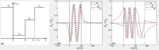
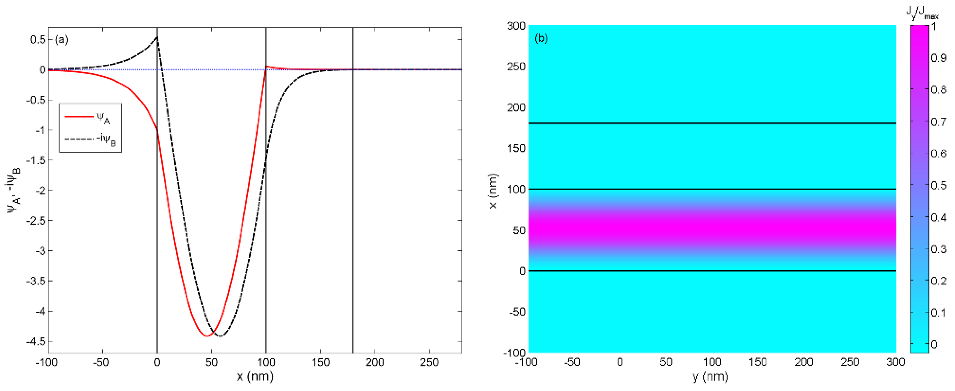
For the case, we have and , which corresponds to the regime of Klein tunneling. Here, we set meV, and there is only one intersection (), as shown in Figure 3a. The corresponding wave function distribution is plotted in Figure 4a. Similar to the optical waveguide, the guided modes is defined by the number of the nodes of the spinor wave function . The spinor components and represent electron and hole states, respectively. It is clearly seen from Figure 4a that there is no fundamental mode in this case since only Klein tunneling occurs in the double-well potential. The probability current density of the guided mode is plotted in Figure 4b, which can be calculated by the definition in the Dirac equation, with , . This finding indicates that the Dirac fermions can be well-localized in the double-well potential.
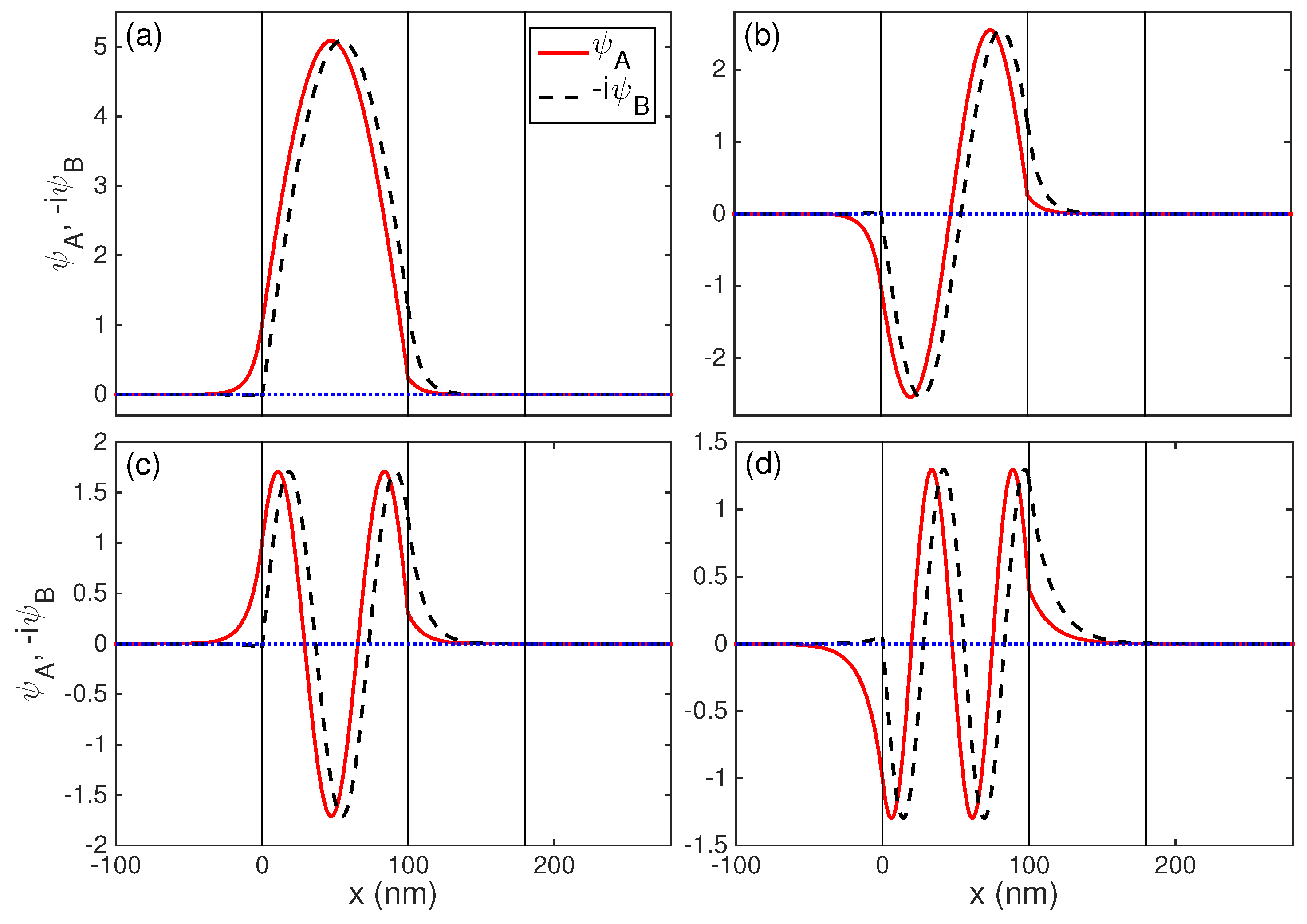
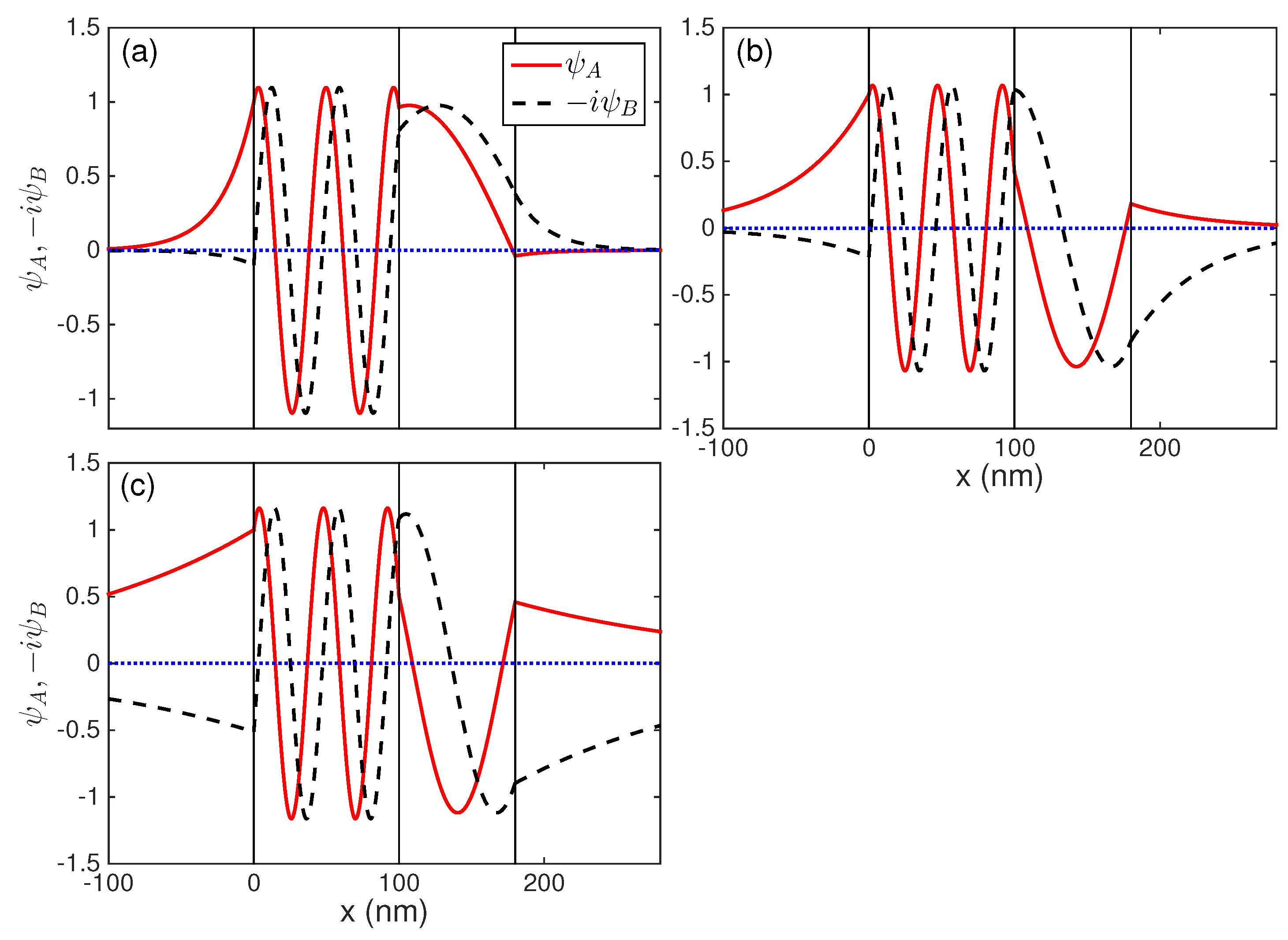
For the case, we have , . Both Klein tunneling and classical motion are present in the double-well potential. Here, we choose meV, and there are four intersections, as shown in Figure 3b. The corresponding wave functions of the four guided modes are presented in Figure 5: (a) ; (b) ; (c) ; and (d) . The figure shows different mode structures and characteristics between and . For , the double-well potential can support the fundamental mode, first-order mode, second-order mode, and third-order mode. However, there is no fundamental mode in the waveguide for (see Figure 5a, a small peak appears in wave functions for on the left interface of the waveguide), and it only supports first-order mode, second-order mode, third-order mode, and fourth-order mode. This finding suggests that the electrons and holes have different behaviors under the same conditions, which is similar to the mixing case of classical motion and Klein tunneling that appeared in an asymmetric quantum well graphene waveguide [9,10].
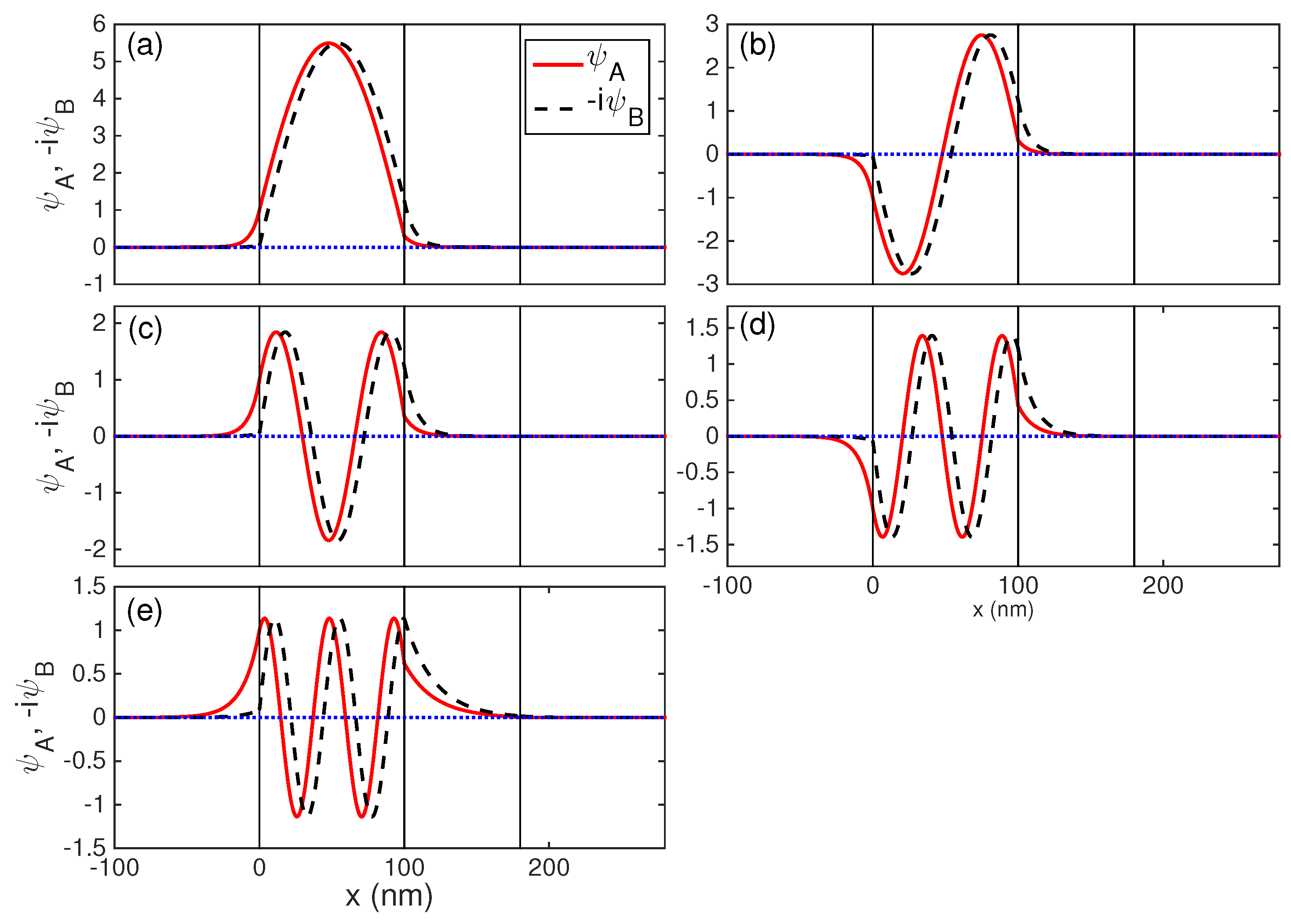
For large electron energy meV in the case, we have . The dependencies of and on are shown in Figure 3c. In this case, it is clearly seen from Figure 6 that the wave functions and of guided modes for the five intersection points: (a) ; (b) ; (c) ; (d) ; and (e) have very similar characteristics. The waveguide can support the fundamental mode, first-order mode, second-order mode, third-order mode, and fourth-order mode for the electrons and the holes. It must be pointed out that the guided modes in region 2 have similar characteristics with those in asymmetric quantum well graphene waveguide [9,10].
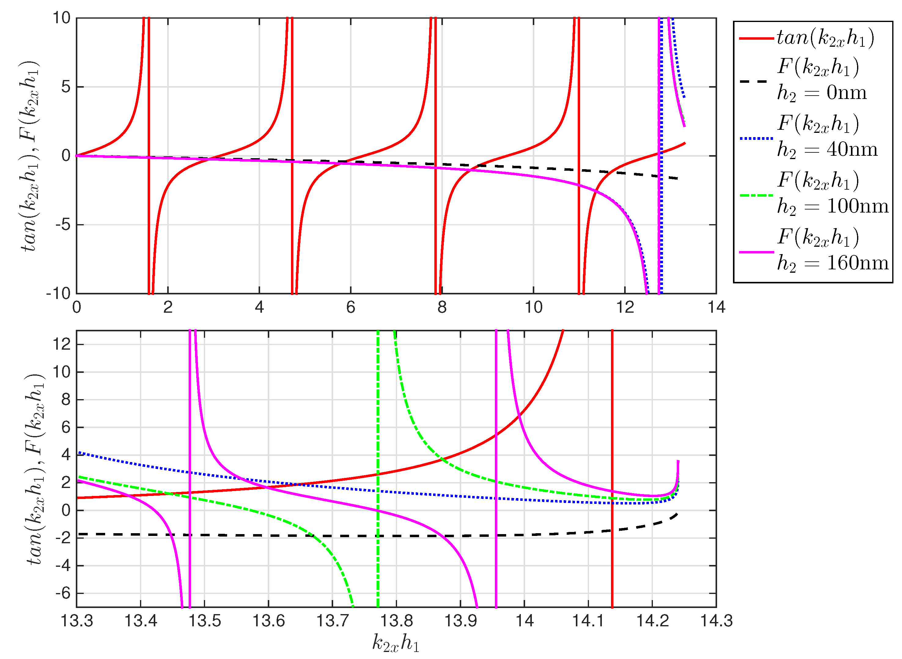
For the guided modes in the region of , , and should be real. The transverse wavenumber in region 2 must fulfills the following condition:
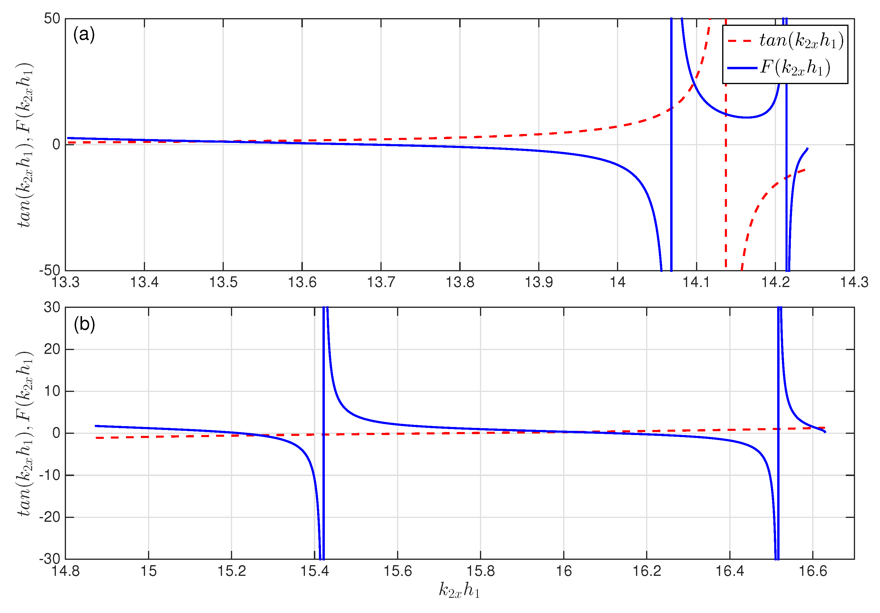
For the incident electrons with low energy meV, the double-well potential cannot support a guided mode. Thus, only a dispersion equation at higher energy meV and meV are plotted in Figure 7a,b, respectively. Each of them has three intersection points. For meV (from Figure 7a), the intersections are (a) ; (b) ; and (c) , which are plotted in Figure 8. For meV (from Figure 7b), we have (a) ; (b) ; and (c) , which are plotted in Figure 9.
From the figure, we see that the electrons and holes have similar mode structure and motion characteristics. For the meV case, the double-well potential is able to support a higher order mode, such as the sixth-order mode (Figure 8b,c). This is known as mode double-degeneracy, which is similar to the oscillating guided modes in a symmetric five-layer left-handed waveguide [46]. For meV, we have fifth-order mode, sixth-order mode, and seventh-order mode, as shown in Figure 9. For completeness, the probability current density of some specific guided modes is plotted in Figure 10, which shows good confinement.
In general, for the electrons in this graphene waveguide with meV, the double-well potential supports the fundamental mode, first-order mode, second-order mode, third-order mode, fifth-order mode and sixth-order mode for , while it supports the first-order mode, second-order mode, third-order mode, fourth-order mode, fifth-order mode and sixth-order mode for . The fourth-order mode is absent for , while the fundamental mode is absent for . Mode double-degeneracy appears for the sixth-order mode for both and . The order of the guided modes is dependent on the incident energy and incidence angle for a given quantum well electron waveguide. The reason for the absence of some guided modes is that the incident energy is not sufficiently large with respect to the critical angle for the certain guided mode [8]. The absence of guided modes is similar to the situations in negative-refractive-index waveguides [46,47]. For the meV case, the guided modes for and have similar mode structure. The waveguide can support the fundamental mode, first-order mode, second-order mode, and up to the seventh-order mode for the electrons and the holes. There is no mode absent in this condition.
For many applications, it is desired to have mode tuning either by potential, the incident energy, or the well width. In Figure 11, the solutions to the guided modes at different values of well width , 40, 100, 160 nm are presented. For the guided modes in , the results (see Figure 11a) show that changing has no effect on the number of guided modes. However, for the guided modes in , we have more guide modes at higher , as shown in Figure 11b. For example, at nm, we have three guided modes in the region , which is higher than two modes for nm, and only one mode for nm. Obviously, there are no intersections for guided modes in the region with nm. In comparison with the quantum well graphene waveguide, the double-well graphene waveguide can support some higher order guided modes in a wider range.
4. Conclusions
We have determined the guided modes in a double-well asymmetry potential with a transfer matrix method over a wide range of parameters. Two types of guide modes were found in the proposed structures, one of which was similar to the characteristics with those in the graphene waveguide with asymmetric quantum well structure. It was found that the proposed graphene based electron waveguides can support some higher order nodes (up to the 7th order). Mode double-degeneracy appeared under some conditions. For some given incident energy of electrons, some modes are absent. Furthermore, the tuning of the number of guided modes by the well width was also studied. These novel properties of the guided modes in the double-well potential may provide potential applications for various graphene-based electronic devices. Electron waveguides are examples of various graphene-based electronic devices; however, the transfer matrix method may not be suitable for simulating other graphene-based electronic devices, such as graphene-based field effect transistors. Hence, we will seek other methods to solve the Dirac equation in graphene in order to simulate graphene-based electronic devices in our future research work.
Acknowledgments
This work is supported by the Singapore Ministry of Education T2 Grant No. T2MOE1401 and the U.S. Air Force Office of Scientific Research (AFOSR) through the Asian Office of Aerospace Research and Development (AOARD) under Grant No. FA2386-14-1-4020.
Author Contributions
Yi Xu and L.K. Ang proposed the idea and presided over the study. Yi Xu and L.K. Ang conceived and calculated the setup. Yi Xu and L.K. Ang wrote the paper. All authors read and approved the final manuscript.
Conflicts of Interest
The authors declare no conflict of interest.
References
- Novoselov, K.S.; Geim, A.K.; Morozov, S.V.; Jiang, D.; Zhang, Y.; Dubonos, S.V.; Grigorieva, I.V.; Firsov, A.A. Electric field effect in atomically thin carbon films. Science 2004, 306, 666–669. [Google Scholar] [CrossRef] [PubMed]
- Beenakker, C.; Sepkhanov, R.; Akhmerov, A.; Tworzydło, J. Quantum Goos-Hänchen effect in graphene. Phys. Rev. Lett. 2009, 102, 146804. [Google Scholar] [CrossRef] [PubMed]
- Sharma, M.; Ghosh, S. Electron transport and Goos–Hänchen shift in graphene with electric and magnetic barriers: Optical analogy and band structure. J. Phys. Condens. Matter 2011, 23, 055501. [Google Scholar] [CrossRef] [PubMed]
- Cheianov, V.V.; Fal’ko, V.; Altshuler, B. The focusing of electron flow and a Veselago lens in graphene pn junctions. Science 2007, 315, 1252–1255. [Google Scholar] [CrossRef] [PubMed]
- Park, C.H.; Son, Y.W.; Yang, L.; Cohen, M.L.; Louie, S.G. Electron beam supercollimation in graphene superlattices. Nano Lett. 2008, 8, 2920–2924. [Google Scholar] [CrossRef] [PubMed]
- Asmar, M.M.; Ulloa, S.E. Rashba spin-orbit interaction and birefringent electron optics in graphene. Phys. Rev. B 2013, 87, 075420. [Google Scholar] [CrossRef]
- Ghosh, S.; Sharma, M. Electron optics with magnetic vector potential barriers in graphene. J. Phys. Condens. Matter 2009, 21, 292204. [Google Scholar] [CrossRef] [PubMed]
- Zhang, F.M.; He, Y.; Chen, X. Guided modes in graphene waveguides. Appl. Phys. Lett. 2009, 94, 212105. [Google Scholar] [CrossRef]
- He, Y.; Xu, Y.; Yang, Y.F.; Huang, W.D. Guided modes in asymmetric graphene waveguides. Appl. Phys. A 2014, 115, 895–902. [Google Scholar] [CrossRef]
- Ping, P.; Peng, Z.; Liu, J.K.; Cao, Z.Z.; Li, G.Q. Oscillating guided modes in graphene-based asymmetric waveguides. Commun. Theor. Phys. 2012, 58, 765. [Google Scholar] [CrossRef]
- Xu, Y.; Ang, L.K. Guided modes in a triple-well graphene waveguide: Analogy of five-layer optical waveguide. J. Opt. 2015, 17, 035005. [Google Scholar] [CrossRef]
- Williams, J.; Low, T.; Lundstrom, M.; Marcus, C. Gate-controlled guiding of electrons in graphene. Nat. Nanotechnol. 2011, 6, 222–225. [Google Scholar] [CrossRef] [PubMed]
- Myoung, N.; Ihm, G.; Lee, S. Magnetically induced waveguide in graphene. Phys. Rev. B 2011, 83, 113407. [Google Scholar] [CrossRef]
- Huang, W.D.; He, Y.; Yang, Y.F.; Li, C.F. Graphene waveguide induced by gradually varied magnetic fields. J. Appl. Phys. 2012, 111, 053712. [Google Scholar] [CrossRef]
- Hartmann, R.R.; Robinson, N.; Portnoi, M. Smooth electron waveguides in graphene. Phys. Rev. B 2010, 81, 245431. [Google Scholar] [CrossRef]
- Wu, Z.H.; Zhai, F.; Peeters, F.; Xu, H.; Chang, K. Valley-dependent Brewster angles and Goos-Hänchen effect in strained graphene. Phys. Rev. Lett. 2011, 106, 176802. [Google Scholar] [CrossRef] [PubMed]
- Villegas, C.E.; Tavares, M.R.; Hai, G.Q.; Peeters, F. Sorting the modes contributing to guidance in strain-induced graphene waveguides. New J. Phys. 2013, 15, 023015. [Google Scholar] [CrossRef]
- Pereira, V.M.; Neto, A.C. Strain engineering of graphene’s electronic structure. Phys. Rev. Lett. 2009, 103, 046801. [Google Scholar] [CrossRef] [PubMed]
- Wu, Z.H. Electronic fiber in graphene. Appl. Phys. Lett. 2011, 98, 082117. [Google Scholar] [CrossRef]
- Pereira, J.M., Jr.; Mlinar, V.; Peeters, F.; Vasilopoulos, P. Confined states and direction-dependent transmission in graphene quantum wells. Phys. Rev. B 2006, 74, 045424. [Google Scholar] [CrossRef]
- Tudorovskiy, T.Y.; Chaplik, A. Spatially inhomogeneous states of charge carriers in graphene. JETP Lett. 2007, 84, 619–623. [Google Scholar] [CrossRef]
- De Martino, A.; Dell’Anna, L.; Egger, R. Magnetic confinement of massless Dirac fermions in graphene. Phys. Rev. Lett. 2007, 98, 066802. [Google Scholar] [CrossRef] [PubMed]
- Low, T.; Guinea, F. Strain-induced pseudomagnetic field for novel graphene electronics. Nano Lett. 2010, 10, 3551–3554. [Google Scholar] [CrossRef] [PubMed]
- Elton, D.M.; Levitin, M.; Polterovich, I. Eigenvalues of a One-Dimensional Dirac Operator Pencil; Annales Henri Poincaré; Springer: Berlin, Germany, 2014; Volume 15, pp. 2321–2377. [Google Scholar]
- Hartmann, R.R.; Portnoi, M. Quasi-exact solution to the Dirac equation for the hyperbolic-secant potential. Phys. Rev. A 2014, 89, 012101. [Google Scholar] [CrossRef]
- Stone, D.; Downing, C.; Portnoi, M. Searching for confined modes in graphene channels: The variable phase method. Phys. Rev. B 2012, 86, 075464. [Google Scholar] [CrossRef]
- Yuan, J.H.; Cheng, Z.; Zeng, Q.J.; Zhang, J.P.; Zhang, J.J. Velocity-controlled guiding of electron in graphene: Analogy of optical waveguides. J. Appl. Phys. 2011, 110, 103706. [Google Scholar] [CrossRef]
- Li, H.D.; Wang, L.; Lan, Z.H.; Zheng, Y.S. Generalized transfer matrix theory of electronic transport through a graphene waveguide. Phys. Rev. B 2009, 79, 155429. [Google Scholar] [CrossRef]
- Pedersen, J.G.; Gunst, T.; Markussen, T.; Pedersen, T.G. Graphene antidot lattice waveguides. Phys. Rev. B 2012, 86, 245410. [Google Scholar] [CrossRef]
- Allen, M.T.; Shtanko, O.; Fulga, I.C.; Akhmerov, A.; Watanabe, K.; Taniguchi, T.; Jarillo-Herrero, P.; Levitov, L.S.; Yacoby, A. Spatially resolved edge currents and guided-wave electronic states in graphene. Nat. Phys. 2016, 12, 128–133. [Google Scholar] [CrossRef]
- Wang, L.G.; Zhu, S.Y. Electronic band gaps and transport properties in graphene superlattices with one-dimensional periodic potentials of square barriers. Phys. Rev. B 2010, 81, 205444. [Google Scholar] [CrossRef]
- Xu, Y.; He, Y.; Yang, Y.F. Transmission gaps in graphene superlattices with periodic potential patterns. Phys. B Condens. Matter 2015, 457, 188–193. [Google Scholar] [CrossRef]
- Xu, Y.; He, Y.; Yang, Y.F.; Zhang, H.F. Electronic band gaps and transport in Cantor graphene superlattices. Superlatt. Microstruct. 2015, 80, 63–71. [Google Scholar] [CrossRef]
- Hanson, G.W. Dyadic Green’s functions and guided surface waves for a surface conductivity model of graphene. J. Appl. Phys. 2008, 103, 064302. [Google Scholar] [CrossRef]
- Tamagnone, M.; Gomez-Diaz, J.; Mosig, J.R.; Perruisseau-Carrier, J. Reconfigurable terahertz plasmonic antenna concept using a graphene stack. Appl. Phys. Lett. 2012, 101, 214102. [Google Scholar] [CrossRef]
- Bouzianas, G.; Kantartzis, N.; Tsiboukis, T. Subcell dispersive finite-difference time-domain schemes for infinite graphene-based structures. IET Microw. Antennas Propag. 2012, 6, 377–386. [Google Scholar] [CrossRef]
- Llatser, I.; Kremers, C.; Cabellos-Aparicio, A.; Jornet, J.M.; Alarcón, E.; Chigrin, D.N. Graphene-based nano-patch antenna for terahertz radiation. Photonics Nanostruct. Fundam. Appl. 2012, 10, 353–358. [Google Scholar] [CrossRef]
- Salonikios, V.; Amanatiadis, S.; Kantartzis, N.; Yioultsis, T. Modal analysis of graphene microtubes utilizing a two-dimensional vectorial finite element method. Appl. Phys. A 2016, 122, 1–7. [Google Scholar] [CrossRef]
- Nayyeri, V.; Soleimani, M.; Ramahi, O.M. Modeling graphene in the finite-difference time-domain method using a surface boundary condition. IEEE Trans. Antennas Propag. 2013, 61, 4176–4182. [Google Scholar] [CrossRef]
- Amanatiadis, S.A.; Kantartzis, N.V.; Tsiboukis, T.D. A loss-controllable absorbing boundary condition for surface plasmon polaritons propagating onto graphene. IEEE Trans. Mag. 2015, 51, 1–4. [Google Scholar] [CrossRef]
- Mock, A. Padé approximant spectral fit for FDTD simulation of graphene in the near infrared. Opt. Mater. Express 2012, 2, 771–781. [Google Scholar] [CrossRef]
- Huard, B.; Sulpizio, J.; Stander, N.; Todd, K.; Yang, B.; Goldhaber-Gordon, D. Transport measurements across a tunable potential barrier in graphene. Phys. Rev. Lett. 2007, 98, 236803. [Google Scholar] [CrossRef] [PubMed]
- Brey, L.; Fertig, H. Electronic states of graphene nanoribbons studied with the Dirac equation. Phys. Rev. B 2006, 73, 235411. [Google Scholar] [CrossRef]
- Mhamdi, A.; Salem, E.B.; Jaziri, S. Electronic reflection for a single-layer graphene quantum well. Solid State Commun. 2013, 175, 106–113. [Google Scholar] [CrossRef]
- Allain, P.E.; Fuchs, J. Klein tunneling in graphene: Optics with massless electrons. Eur. Phys. J. B 2011, 83, 301–317. [Google Scholar] [CrossRef]
- He, Y.; Zhang, J.; Li, C.F. Guided modes in a symmetric five-layer left-handed waveguide. J. Opt. Soc. Am. B 2008, 25, 2081–2091. [Google Scholar] [CrossRef]
- Shadrivov, I.V.; Sukhorukov, A.A.; Kivshar, Y.S. Guided modes in negative-refractive-index waveguides. Phys. Rev. E 2003, 67, 057602. [Google Scholar] [CrossRef] [PubMed]
Figure 1.
Schematic diagram of (a) a double-well potential on graphene; (b) guided modes in the region ; (c) guided modes in the region .
Figure 1.
Schematic diagram of (a) a double-well potential on graphene; (b) guided modes in the region ; (c) guided modes in the region .

Figure 2.
The critical angle as a function of the incidence energy E. The physical parameters are: meV, meV, meV, nm, nm.
Figure 2.
The critical angle as a function of the incidence energy E. The physical parameters are: meV, meV, meV, nm, nm.

Figure 3.
Graphical determination of for guided modes in . The red and blue curves correspond to and , respectively. The energy of incident electron is (a) meV; (b) meV; and (c) meV. The other parameters are the same as those in Figure 2.
Figure 3.
Graphical determination of for guided modes in . The red and blue curves correspond to and , respectively. The energy of incident electron is (a) meV; (b) meV; and (c) meV. The other parameters are the same as those in Figure 2.
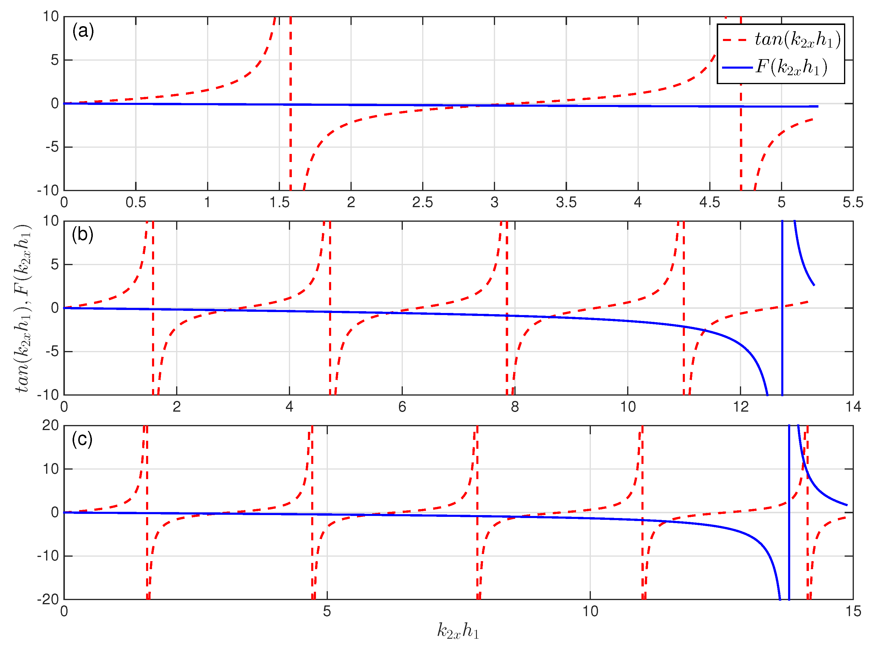
Figure 4.
(a) the wave function of guided modes as a function of distance corresponding to the intersection in Figure 3a. The solid curve and the dashed lines corresponds to and , respectively. The vertical lines represent the boundaries of the waveguide; and (b) the corresponding probability current density within the graphene waveguide for the guided mode. The solid black lines represent boundaries of the waveguide.

Figure 5.
The wave function (solid) and (dashed) of guided modes as a function of distance corresponding to the intersections in Figure 3b: (a) , ; (b) , ; (c) , ; and (d) , .
Figure 5.
The wave function (solid) and (dashed) of guided modes as a function of distance corresponding to the intersections in Figure 3b: (a) , ; (b) , ; (c) , ; and (d) , .

Figure 6.
The wave function (solid) and (dashed) of guided modes as a function of distance corresponding to the intersections in Figure 3c: (a) , ; (b) , ; (c) , ; (d) , ; and (e) , .
Figure 6.
The wave function (solid) and (dashed) of guided modes as a function of distance corresponding to the intersections in Figure 3c: (a) , ; (b) , ; (c) , ; (d) , ; and (e) , .

Figure 7.
Graphical determination of for guided modes in . The red and blue curves correspond to and , respectively. The energy of incident electron is (a) meV and (b) meV. The other parameters are the same as those in Figure 2.
Figure 7.
Graphical determination of for guided modes in . The red and blue curves correspond to and , respectively. The energy of incident electron is (a) meV and (b) meV. The other parameters are the same as those in Figure 2.

Figure 8.
The wave function (solid) and (dashed) of guided modes as a function of distance corresponding to the intersections in Figure 7a: (a) , ; (b) , ; and (c) , .
Figure 8.
The wave function (solid) and (dashed) of guided modes as a function of distance corresponding to the intersections in Figure 7a: (a) , ; (b) , ; and (c) , .

Figure 9.
The wave function (solid) and (dashed) of guided modes as a function of distance corresponding to the intersections in Figure 7b: (a) , ; (b) , ; and (c) , .
Figure 9.
The wave function (solid) and (dashed) of guided modes as a function of distance corresponding to the intersections in Figure 7b: (a) , ; (b) , ; and (c) , .
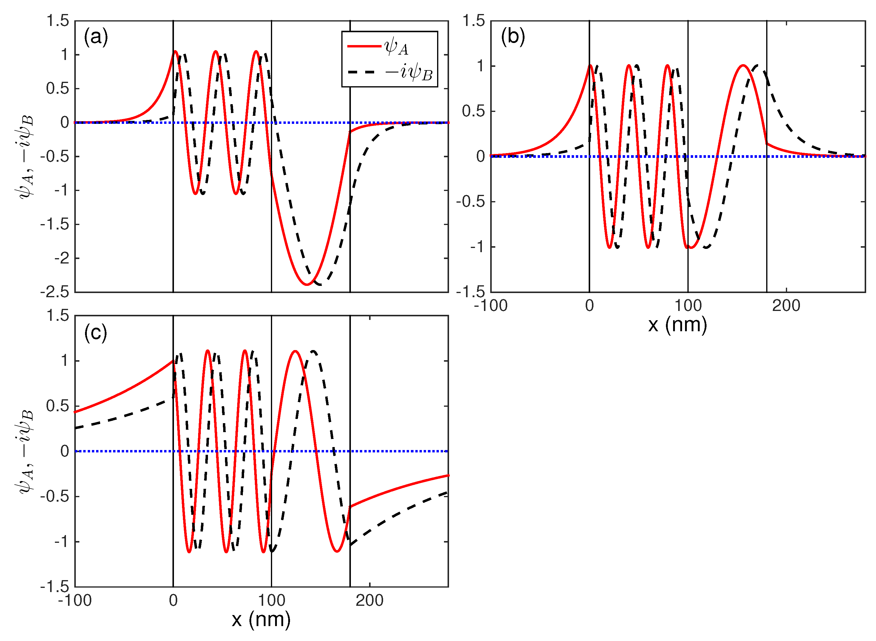
Figure 10.
Probability current density within the graphene waveguide for the guided modes: (a) meV, ; (b) meV, ; (c) meV, ; and (d) meV, .
Figure 10.
Probability current density within the graphene waveguide for the guided modes: (a) meV, ; (b) meV, ; (c) meV, ; and (d) meV, .
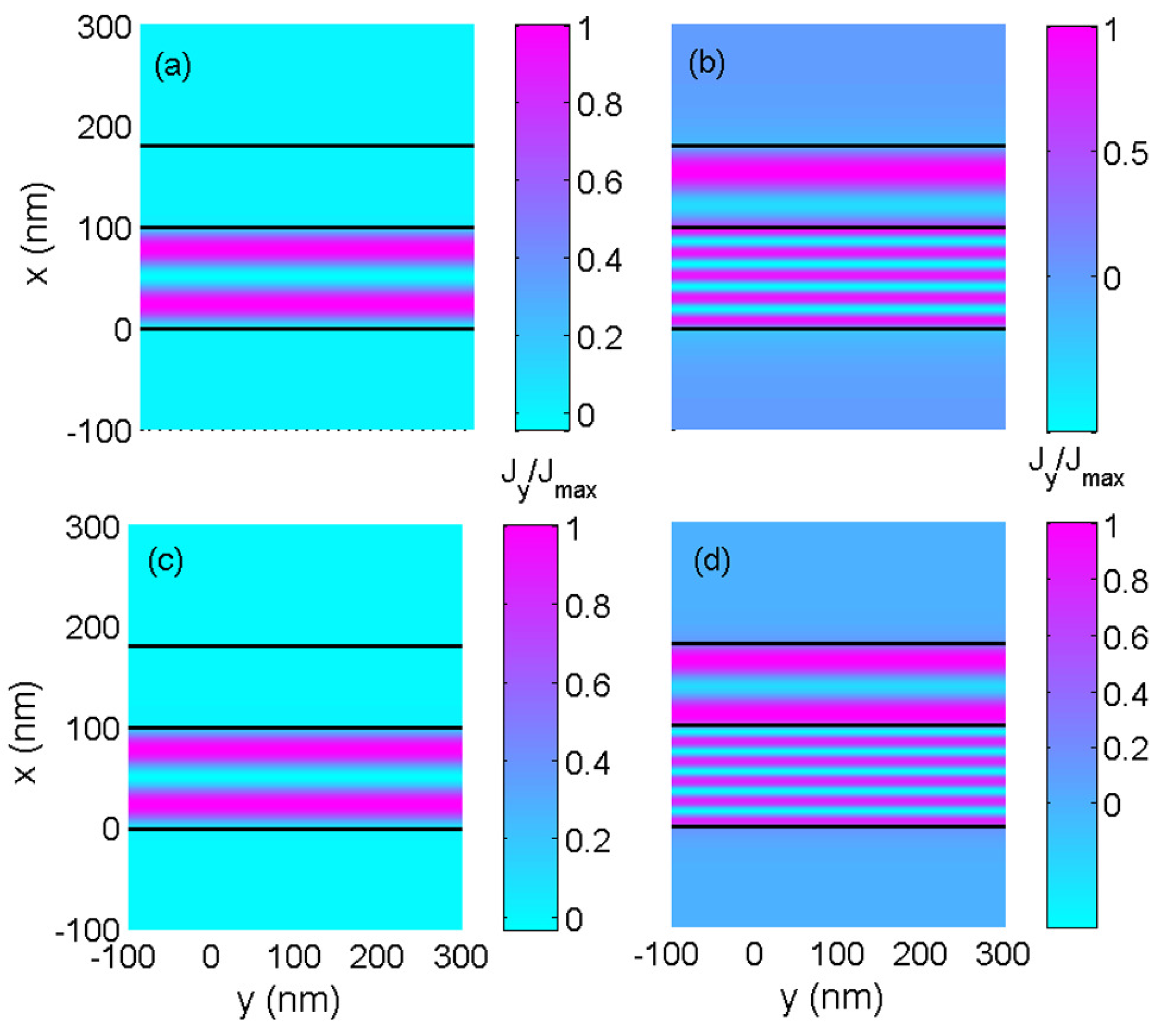
Figure 11.
Graphical determination of and for guided modes in (a) and (b) with different values of . Here, the incident energy of electrons is fixed at meV. The other parameters are the same as those in Figure 2.
Figure 11.
Graphical determination of and for guided modes in (a) and (b) with different values of . Here, the incident energy of electrons is fixed at meV. The other parameters are the same as those in Figure 2.

© 2016 by the authors; licensee MDPI, Basel, Switzerland. This article is an open access article distributed under the terms and conditions of the Creative Commons Attribution (CC-BY) license (http://creativecommons.org/licenses/by/4.0/).
Share and Cite
MDPI and ACS Style
Xu, Y.; Ang, L.K. Guided Modes in a Double-Well Asymmetric Potential of a Graphene Waveguide. Electronics 2016, 5, 87. https://doi.org/10.3390/electronics5040087
AMA Style
Xu Y, Ang LK. Guided Modes in a Double-Well Asymmetric Potential of a Graphene Waveguide. Electronics. 2016; 5(4):87. https://doi.org/10.3390/electronics5040087
Chicago/Turabian StyleXu, Yi, and Lay Kee Ang. 2016. "Guided Modes in a Double-Well Asymmetric Potential of a Graphene Waveguide" Electronics 5, no. 4: 87. https://doi.org/10.3390/electronics5040087
Note that from the first issue of 2016, this journal uses article numbers instead of page numbers. See further details here.