
Atomic Layer Growth of InSe and Sb2Se3 Layered Semiconductors and Their Heterostructure

Department of Physics, Portland State University, Portland, OR 97207, USA
*
Authors to whom correspondence should be addressed.
Electronics 2017, 6(2), 27; https://doi.org/10.3390/electronics6020027
Submission received: 12 February 2017
/
Revised: 19 March 2017
/
Accepted: 27 March 2017
/
Published: 30 March 2017
(This article belongs to the Special Issue Two-Dimensional Electronics and Optoelectronics)
Abstract
:Metal chalcogenides based on the C–M–M–C (C = chalcogen, M = metal) structure possess several attractive properties that can be utilized in both electrical and optical devices. We have shown that specular, large area films of γ-InSe and Sb2Se3 can be grown via atomic layer deposition (ALD) at relatively low temperatures. Optical (absorption, Raman), crystalline (X-ray diffraction), and composition (XPS) properties of these films have been measured and compared to those reported for exfoliated films and have been found to be similar. Heterostructures composed of a layer of γ-InSe (intrinsically n-type) followed by a layer of Sb2Se3 (intrinsically p-type) that display diode characteristics were also grown.
1. Introduction
The unique properties of graphene have drawn attention to other 2-dimensional (2D) materials, in particular metal chalcogenides, which can behave as metals, insulators, or semiconductors [1,2,3]. These semiconductors are of particular interest for the fabrication of the future generation of field effect transistors (FETs) and optoelectronic devices. These layered materials can be used as single or a few atomic layer thick films, absent of dangling bonds which allows for better electrostatic control of carrier transport; hence, they are ideal for downscaling of FETs. The ability to tune the direct band gap of many of these materials, by controlling their thickness, allows further flexibility for the design and fabrication of optoelectronic devices. However, to date, most attention has been focused on 2D transition metal dichalcogenides of structure C–M–C (C = chalcogen, M = metal), where one metal atom is sandwiched between two chalcogen atoms [4,5,6,7]. There are other forms of metal chalcogenides that are equally intriguing. Among these is the C–M–M–C family, which has been drawing more attention [8,9]. These materials have been used to produce photocatalysts, photo-detectors, image sensors, and transistors with high electron mobility [10,11,12,13]. We are currently investigating 2D semiconductor layers of this family of chalcogenide material that are composed of two metal and two Se atoms, Se–M–M–Se (M = In, Sb) grown via atomic layer deposition (ALD). Our objective is to demonstrate the growth of uniform, large area films that may in the future be utilized for the fabrication of electronic and optical devices. Our objective in this communication is to demonstrate that uniform and smooth films of InSe and Sb2Se3, both belonging to the C–M–M–C family of metal chalcogenides, can be grown over large areas using ALD. The properties of thin films grown using this approach, and their heterostructure are presented below.
InSe has several polytypes, however the β -phase and γ -phase are the two common forms of its crystal structure [14]. In this work, only the γ-InSe phase is considered which crystallizes into stacked hexagonal layers. The vertical stacking of this material is composed of Se–In–In–Se sheets, where each sheet is weakly bound to its neighboring sheets by the van der Waals force [14]. It is interesting to note that while bulk InSe has a direct band gap (1.2 eV), reduction of its thickness first leads to a wider band gap due to quantum confinement, however further reduction of the thickness to a few layers results in a strong decrease of the photoluminescence. One of the reasons for this attenuation has been attributed to direct-to-indirect bandgap crossover, while another explanation has been attributed to the enhancement of non-radiative recombination processes in the thin flakes [15,16]. To date, InSe films have been produced mostly via chemical vapor deposition (CVD), sputtering, exfoliation, and electrodeposition [15,17,18,19,20]. In these cases, the films are either small, on the order of a few tens of micrometers per side (exfoliation) or are composed of flakes or platelets.
Unlike InSe, Sb2Se3 is a narrow band gap, layered metal chalcogenide (Se–Sb–Sb–Se) that has a single phase [21]. It is a direct band gap semiconductor with a layered structure and an orthorhombic structure [22]. The films consist of staggered, parallel layers of 1D (Sb4Se6)n ribbons that are composed of strong Sb–Se bonds along the [001] direction. In the [100] and [010] directions, the ribbons are held in the stack by the weak van der Waals forces [23]. It has received attention as a thermoelectric material, and recently as a light sensitizer in photovoltaic devices because of its narrow band gap of about 1.1 eV–1.3 eV, which approaches the ideal Shockley−Queisser value [24,25,26]. These films have been produced via a number of methods, including thermal evaporation, chemical bath deposition, spray pyrolysis, pulsed laser deposition and electrochemical deposition [25,27,28,29,30].
2. Materials and Methods
InSe and Sb2Se3 films were grown in a Microchemistry F-120 ALD reactor (Microchemistry, Helsinki, Finland) that can handle two 50 mm × 50 mm substrates per run. The substrates for these films consisted of either p-or n-type Si wafers coated with a 320 nm thick film of thermal silicon oxide. Besides Si, plain glass slides and fluorinated tin oxide (FTO) coated glass plates were also used as substrates. The precursors for InSe growth were InCl3 and H2Se (8%, balance Ar). The In source temperature was set at 110 °C and the carrier gas was nitrogen. The pulse sequence per cycle was as follows; InCl3 pulse width of 1 s; N2 purge of 1.0 s; H2Se pulse width of 1.5 s; followed by 1.0 s N2 purge. Uniform film growth occurred over a temperature range of 310 °C to 380 °C. The films reported here were grown at 350 °C, where the growth rate was 0.05 nm per cycle. The pulse sequence for Sb2Se3 films was SbCl3 (1 s), N2 (1.5 s), H2Se (1.5 s), and N2 (1.5 s). Uniform films were produced over a temperature range of 270 °C to 320 °C. From this range, 300 °C was selected to grow the films, where the growth rate was 0.22 nm/cycle. Optimization of growth conditions was done mostly based on Raman analysis, which offered a quick turn-around. Besides Raman, the crystalline structure of these films was examined with X-ray diffraction (XRD) (Rigaku Corp., Tokyo, Japan), their composition with X-ray photoelectron spectroscopy (XPS) (Northrop-Grumman, Falls Church, VA, USA) and their band gaps with optical absorption. The surfaces of these films were examined with a scanning electron microscope (SEM) (FEI Corp, Hillsboro, OR, USA) and found to be featureless. Finally, InSe/Sb2Se3 heterostructures were grown and their current-voltage (I–V) profiles were examined.
3. Results
The surface morphology of the films was first checked with a Nomarski microscope and then with an SEM. When the growth process was optimized, the surfaces of both InSe and Sb2Se3 were smooth and featureless, as shown in Figure 1a,b. This is a major difference between films grown via ALD and other methods. Although we expect there to be grain boundaries, we were unable to detect them with the SEM. Also, no grain boundaries were visible with the electron backscatter diffraction (EBSD) method.
The crystalline properties of the films were characterized using grazing-angle (0.5°) XRD. The XRD spectrum of a 17 nm thick InSe film is shown in Figure 2a. The spectrum is dominated by the [006] peak, followed by minor peaks, which are characteristic of the hexagonal structure of γ-InSe (JCPDS 40-1407). Also, the deposition of an orange film on the walls of the reactor is indicative of this phase of the InSe [31].
The XRD spectrum of our antimonselite (Sb2Se3) film is shown in Figure 2b, where all of the diffraction peaks agree well with its orthorhombic crystal structure (JCPDS 15-0861). Major peaks are indexed to the diffraction planes. The crystal lattice parameters were calculated as a = 1.159 nm, b = 1.175 nm, and c = 0.3949 nm, that are consistent with the values reported in literature [32]. No peaks of any other phases were detected, which indicates that these films are of single phase and high purity.
Optical characterization involved Raman spectroscopy and absorption spectra of these films. The Raman spectrum of a 17 nm thick InSe film is shown in Figure 3a, where the excitation wavelength was 532 nm. It shows the signature peaks corresponding to both the in-plane (E) and out-of-plane (A) modes that are consistent with those reported for flakes of γ-InSe [15,18,33,34]. Comparing the InSe data in Figure 3a with published results for the bulk and thin films, we can identify the peaks at about 117 cm−1, 175 cm−1, and 205 cm−1 with A’1, E’2g, and A’1(LO) Raman modes, respectively. The peak at 205 cm−1 is strongest in films that are at about 6 nm to 9 nm thick layers and then attenuates with increase in thickness. The peak at around 155 cm−1 is distinctive for the γ phase of InSe and is related to the zone center mode of the crystal [35,36].
The Raman spectrum of the 15 nm thick Sb2Se3 thin film is shown in Figure 3b. It agrees well with previously reported data, where the main peak at 189 cm−1 (A21g) is the characteristic Sb–Se stretching mode of the SbSe3/2 pyramids. The two other peaks, at about 151 cm−1 (A22u) and at about 125 cm−1 (E2g) are associated with the Sb–Sb bonds and Se–Se bonds, respectively [37,38,39].
Band gaps of these films were determined from their respective absorption spectra obtained from the films deposited on glass substrates. The absorbance of these films was recorded over a spectral range of 300 to 1100 nm. Plots of the wavelength (in terms of energy E in eV) versus the absorbance InSe and Sb2Se3 films are plotted in Figure 4a,b, respectively. The intercept on the x-axis of the extrapolation of the linear portion of the slope corresponds to the band gap of the material. For the 17 nm thick InSe film, the intercept occurs at about 2.35 eV. This value is in good agreement with the band gap of γ-InSe, which is defined as the transition between the px and py orbital to the bottom of the conduction band that corresponds to an energy gap of 2.4 eV [15,18]. The band gap of γ-InSe is higher than the other phases, therefore this parameter can be used to discriminate it from the other phases [35]. From Figure 4b, a band gap value of 1.3 eV was determined for a 15 nm thick Sb2Se3 film. This value is within the range of 1.1 to 1.3 eV previously reported [21,40].
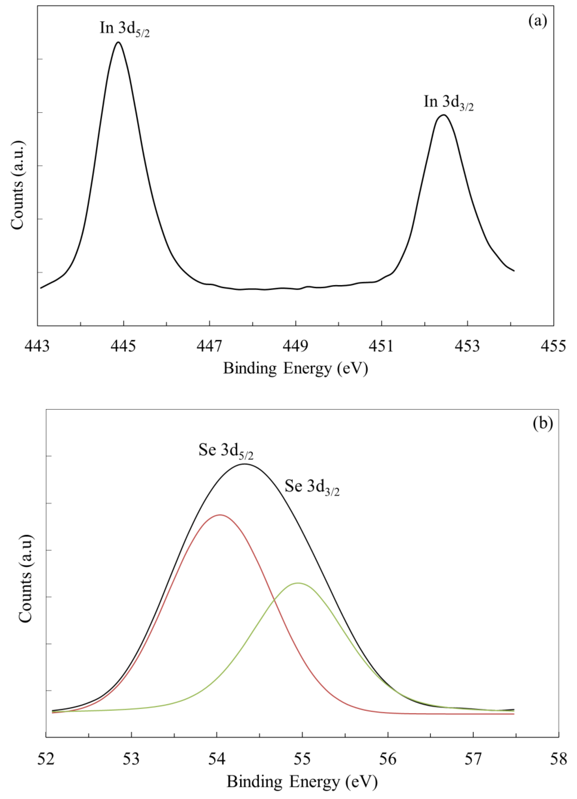
The chemical composition of both of these films was examined by X-ray photoelectron spectroscopy (XPS). The signature binding energies of In 3d5/2 and In 3d3/2, shown in Figure 5a, correspond to 452.47 eV and 444.88 eV, respectively. The Se 3d profile is deconvoluted to show the two, closely spaced binding profiles of the Se d5/2 and d3/2 of binding energies of 53.88 eV and 54.88 eV (Figure 5b). These values are in agreement with pure In2Se3 films [41]. The dip between the two peaks is an indication of oxidation of the films, which is not surprising since the samples were exposed to air for a short period of time before XPS analysis.
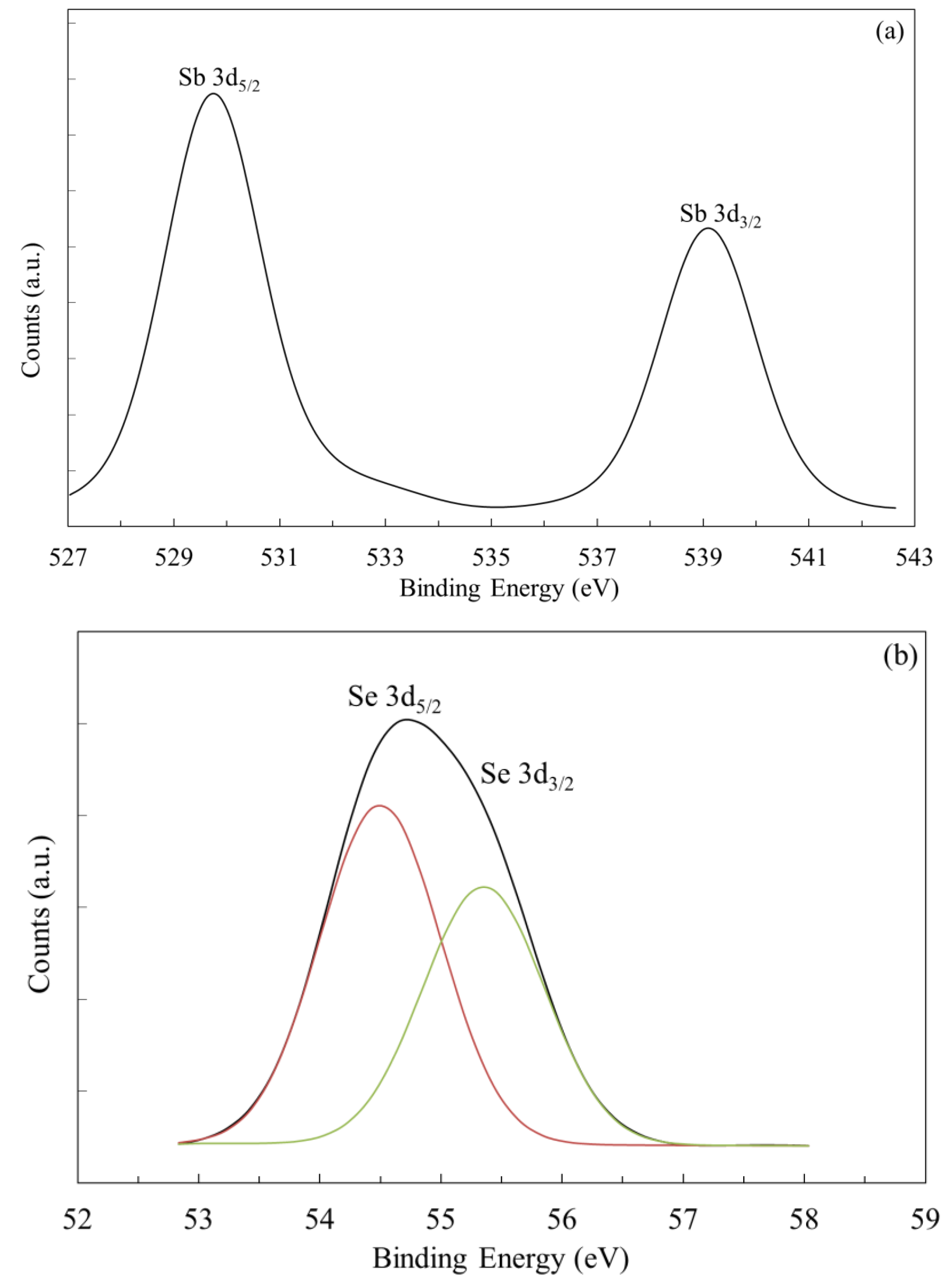
The XPS binding energy of Sb2Se3 is shown in Figure 6. The binding energies of Sb 3d5/2 and 3d3/2 are 529.83 eV and 539.03 eV as shown in Figure 6a. Detailed spectral deconvolution of the Se 3d high resolution XPS spectrum revealed that the binding energy of Se 3d5/2 and 3d3/2 are 54.43 eV and 55.23 eV, respectively, which is in good agreement with the expected binding energy of Sb2Se3 [25]. These binding energies were corrected by referencing the C 1s peak to 284.70 eV.
4. Discussion
In an ALD process, the choice of the precursors and substrates is important in order to produce a saturated chemisorbed layer of the first species during the initial phase of the growth [42]. Moreover, the deposition parameters such as the pulse widths and temperature must be optimized to produce this condition. Then, the growth will proceed layer by layer, which is ideal for growth of a 2D film. We have found that organometallic or chloride-based metal precursors (with sufficient vapor pressure) work well on SiO2 covered substrates, as we have previously demonstrated with other metal chalcogenides [5,43,44].
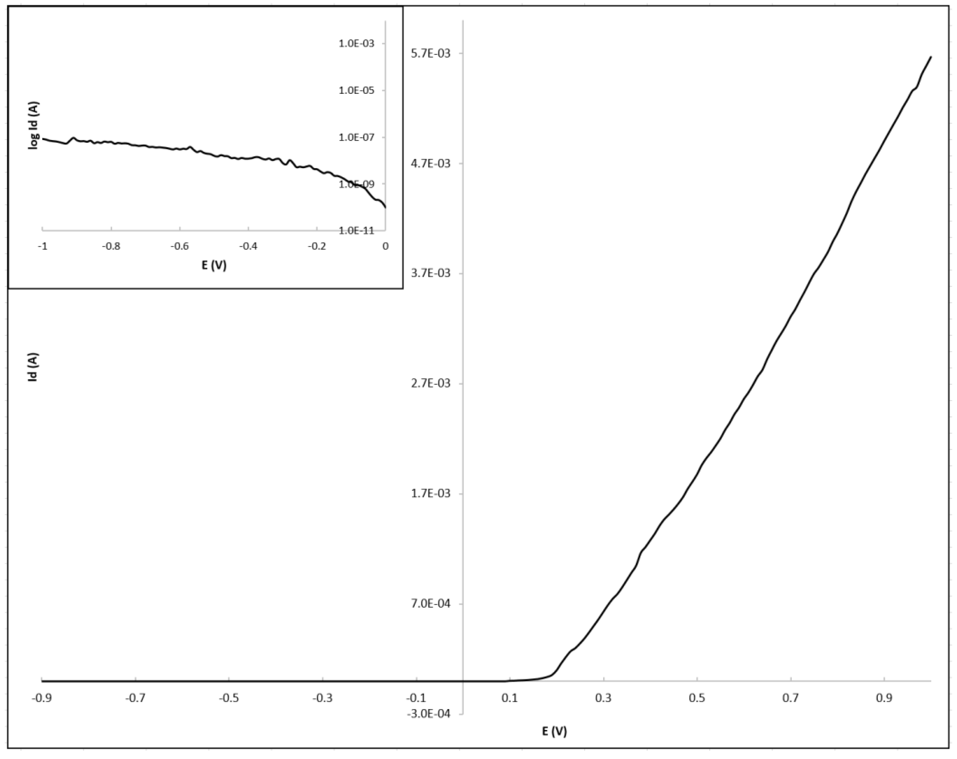
The 2D materials, as described above, are composed of individual layers that are held together by the weak van der Waals force. Within each layer, the atoms are strongly bonded to each other in 2D via either valence or ionic bonds, and in the absence of dangling bonds. This allows stacking of two different 2D materials with different physical properties, crystalline parameters and crystal symmetry to grow heterojunctions and superlattices held together by the van der Waals force. This approach to grow 2D heterojunctions has been referred to as van der Waals epitaxy [45]. We have grown heterostructures composed of 5 nm–10 nm thick InSe and 5 nm–7 nm thick Sb2Se3 layers by sequentially growing each layer on Si/SiO2 substrates and FTO-coated glass substrates. While detailed electrical characterization of these films is underway, Hall effect was used to determine the intrinsic doping properties of each of these two films. The InSe films were found to be intrinsically n-type and Sb2Se3 were intrinsically p-type. On the FTO substrates, the first film deposited was InSe, followed by Sb2Se3, while keeping one part of the FTO surface covered to avoid any deposition. Small Au contacts were sputtered on top of the Sb2Se3 layer and Al on the FTO portion. The current–voltage (I–V) profiles of these samples were then examined.
A typical example of one of these samples is shown in Figure 7, which shows the characteristic profile of a pn diode. The leakage current with a reverse bias is shown (in log scale) in the inset. A maximum leakage current of 10−7 A was measured at −1 V bias. Since each precursor was introduced separately into the reactor for a surface reaction for a layer-by-layer growth, and we were working at a relatively low temperature, we do not expect significant intermixing at the interface. This heterojunction was grown at 310 °C, which overlaps the optimum range of both the materials. A one minute purge was introduced before starting the Sb2Se3 layer to ensure a sharp interface. In our previous work on SnS/WS2 heterojunctions that were grown at a slightly higher temperature, there were no obvious signs of intermixing at the interface [5].
5. Conclusions
In summary, ALD has been utilized to grow smooth and continuous layers of γ-InSe and Sb2Se3 layered metal chalcogenide on SiO2-coated Si and glass substrates. Crystalline and optical properties, as well as the composition of these films are comparable to those produced by other means, especially exfoliation. The InSe and Sb2Se3 films show intrinsic n-type and p-type behaviors, respectively. A combination of these two films shows pn diode characteristics. These results show that ALD offers a viable path for producing large area films of metal chalcogenides for future industrial scale applications.
Author Contributions
Robert Browning, Neal Kuperman, Bill Moon and Raj Solanki all contributed equally.
Conflicts of Interest
The authors declare no conflict of interest.
References
- Chhowalla, M.; Shin, H.S.; Eda, G.; Li, L.J.; Loh, K.P.; Zhang, H. The chemistry of two-dimensional layered transition metal dichalcogenide nanosheets. Nat. Chem. 2013, 5, 263–275. [Google Scholar] [CrossRef] [PubMed]
- Xu, M.; Liang, T.; Shi, M.; Chen, H. Graphene-like two-dimensional materials. Chem. Rev. 2013, 113, 3766–3798. [Google Scholar] [CrossRef] [PubMed]
- Geim, A.K.; Grigorieva, I.V. Van der waals heterostructures. Nature 2013, 499, 419–425. [Google Scholar] [CrossRef] [PubMed]
- Wang, Q.H.; Kalantar-Zadeh, K.; Kis, A.; Coleman, J.N.; Strano, M.S. Electronics and optoelectronics of two-dimensional transition metal dichalcogenides. Nat. Nanotechnol. 2012, 7, 699–712. [Google Scholar] [CrossRef] [PubMed]
- Browning, R.; Plachinda, P.; Padigi, P.; Solanki, R.; Rouvimov, S. Growth of multiple ws2/sns layered semiconductor heterojunctions. Nanoscale 2016, 8, 2143–2148. [Google Scholar] [CrossRef] [PubMed]
- Das, S.; Chen, H.Y.; Penumatcha, A.V.; Appenzeller, J. High performance multilayer mos2 transistors with scandium contacts. Nano Lett. 2013, 13, 100–105. [Google Scholar] [CrossRef] [PubMed]
- Radisavljevic, B.; Radenovic, A.; Brivio, J.; Giacometti, V.; Kis, A. Single-layer mos2 transistors. Nat. Nanotechnol. 2011, 6, 147–150. [Google Scholar] [CrossRef] [PubMed]
- Li, X.; Lin, M.W.; Puretzky, A.A.; Idrobo, J.C.; Ma, C.; Chi, M.; Yoon, M.; Rouleau, C.M.; Kravchenko, I.I.; Geohegan, D.B.; et al. Controlled vapor phase growth of single crystalline, two-dimensional gase crystals with high photoresponse. Sci. Rep. 2014, 4, 5497. [Google Scholar] [PubMed]
- Luxa, J.; Wang, Y.; Sofer, Z.; Pumera, M. Layered post-transition-metal dichalcogenides (x-m-m-x) and their properties. Chemistry 2016, 22, 18810–18816. [Google Scholar] [CrossRef] [PubMed]
- Feng, W.; Zheng, W.; Cao, W.; Hu, P. Back gated multilayer inse transistors with enhanced carrier mobilities via the suppression of carrier scattering from a dielectric interface. Adv. Mater. 2014, 26, 6587–6593. [Google Scholar] [CrossRef] [PubMed]
- Lei, S.; Wen, F.; Li, B.; Wang, Q.; Huang, Y.; Gong, Y.; He, Y.; Dong, P.; Bellah, J.; George, A.; et al. Optoelectronic memory using two-dimensional materials. Nano Lett. 2015, 15, 259–265. [Google Scholar] [CrossRef] [PubMed]
- Harvey, A.; Backes, C.; Gholamvand, Z.; Hanlon, D.; McAteer, D.; Nerl, H.C.; McGuire, E.; Seral-Ascaso, A.; Ramasse, Q.M.; McEvoy, N.; et al. Preparation of gallium sulfide nanosheets by liquid exfoliation and their application as hydrogen evolution catalysts. Chem. Mater. 2015, 27, 3483–3493. [Google Scholar] [CrossRef]
- Hu, P.; Wen, Z.; Wang, L.; Tan, P.; Xiao, K. Synthesis of few-layer gase nanosheets for high performance photodetectors. ACS Nano 2012, 6, 5988–5994. [Google Scholar] [CrossRef] [PubMed]
- Amory, C.; Bernède, J.C.; Marsillac, S. Study of a growth instability of γ-in2se3. J. Appl. Phys. 2003, 94, 6945–6948. [Google Scholar] [CrossRef]
- Sánchez-Royo, J.F.; Muñoz-Matutano, G.; Brotons-Gisbert, M.; Martínez-Pastor, J.P.; Segura, A.; Cantarero, A.; Mata, R.; Canet-Ferrer, J.; Tobias, G.; Canadell, E.; et al. Electronic structure, optical properties, and lattice dynamics in atomically thin indium selenide flakes. Nano Res. 2014, 7, 1556–1568. [Google Scholar] [CrossRef]
- Mudd, G.W.; Svatek, S.A.; Ren, T.; Patane, A.; Makarovsky, O.; Eaves, L.; Beton, P.H.; Kovalyuk, Z.D.; Lashkarev, G.V.; Kudrynskyi, Z.R.; et al. Tuning the bandgap of exfoliated inse nanosheets by quantum confinement. Adv. Mater. 2013, 25, 5714–5718. [Google Scholar] [CrossRef] [PubMed]
- Shigeru, S.; Tesuo, I. Crystalline inse films prepared by rf-sputtering technique. Jpn. J. Appl. Phys. 1991, 30, L2127. [Google Scholar]
- Lei, S.; Ge, L.; Najmaei, S.; George, A.; Kappera, R.; Lou, J.; Chhowalla, M.; Yamaguchi, H.; Gupta, G.; Vajtai, R.; et al. Evolution of the electronic band structure and efficient photo-detection in atomic layers of inse. ACS Nano 2014, 8, 1263–1272. [Google Scholar] [CrossRef] [PubMed]
- Stoll, S.L.; Barron, A.R. Metal− organic chemical vapor deposition of indium selenide thin films. Chem. Mater. 1998, 10, 650–657. [Google Scholar] [CrossRef]
- Ho, C.H.; Lin, C.H.; Wang, Y.P.; Chen, Y.C.; Chen, S.H.; Huang, Y.S. Surface oxide effect on optical sensing and photoelectric conversion of alpha-in2se3 hexagonal microplates. ACS Appl. Mater. Interfaces 2013, 5, 2269–2277. [Google Scholar] [CrossRef] [PubMed]
- Ghosh, G. The sb-se (antimony-selenium) system. J. Phase Equilibria 1993, 14, 753–763. [Google Scholar] [CrossRef]
- Chang, H.-W.; Sarkar, B.; Liu, C.W. Synthesis of sb2se3 nanowires via a solvothermal route from the single source precursor sb[se2p(oipr)2]3. Cryst. Growth Des. 2007, 7, 2691–2695. [Google Scholar] [CrossRef]
- Zhou, Y.; Wang, L.; Chen, S.; Qin, S.; Liu, X.; Chen, J.; Xue, D.-J.; Luo, M.; Cao, Y.; Cheng, Y.; et al. Thin-film sb2se3 photovoltaics with oriented one-dimensional ribbons and benign grain boundaries. Nat. Photonics 2015, 9, 409–415. [Google Scholar] [CrossRef]
- Kutasov, V.A. Shifting the maximum figure-of-merit of (bi, sb)2(te, se)3 thermoelectrics to lower temperatures. In Thermoelectrics Handbook; CRC Press: Boca Raton, FL, USA, 2005; pp. 37-18–37-31. [Google Scholar]
- Liu, X.; Chen, J.; Luo, M.; Leng, M.; Xia, Z.; Zhou, Y.; Qin, S.; Xue, D.J.; Lv, L.; Huang, H.; et al. Thermal evaporation and characterization of sb2se3 thin film for substrate sb2se3/cds solar cells. ACS Appl. Mater. Interfaces 2014, 6, 10687–10695. [Google Scholar] [CrossRef] [PubMed]
- Shockley, W.; Queisser, H.J. Detailed balance limit of efficiency of p-n junction solar cells. J. Appl. Phys. 1961, 32, 510–519. [Google Scholar] [CrossRef]
- Rajpure, K.; Bhosale, C. Effect of se source on properties of spray deposited sb 2 se 3 thin films. Mater. Chem. Phys. 2000, 62, 169–174. [Google Scholar] [CrossRef]
- Rodriguez-Lazcano, Y.; Peña, Y.; Nair, M.; Nair, P. Polycrystalline thin films of antimony selenide via chemical bath deposition and post deposition treatments. Thin Solid Films 2005, 493, 77–82. [Google Scholar] [CrossRef]
- Fernandez, A.; Merino, M. Preparation and characterization of sb 2 se 3 thin films prepared by electrodeposition for photovoltaic applications. Thin Solid Films 2000, 366, 202–206. [Google Scholar] [CrossRef]
- Xue, M.-Z.; Fu, Z.-W. Pulsed laser deposited sb 2 se 3 anode for lithium-ion batteries. J. Alloys Compd. 2008, 458, 351–356. [Google Scholar] [CrossRef]
- Tabernor, J.; Christian, P.; O'Brien, P. A general route to nanodimensional powders of indium chalcogenides. J. Mater. Chem. 2006, 16, 2082. [Google Scholar] [CrossRef]
- Tideswell, N.W.; Kruse, F.H.; McCullough, J.D. The crystal structure of antimony selenide, sb2se3. Acta Crystallogr. 1957, 10, 99–102. [Google Scholar] [CrossRef]
- Chen, Z.; Gacem, K.; Boukhicha, M.; Biscaras, J.; Shukla, A. Anodic bonded 2d semiconductors: From synthesis to device fabrication. Nanotechnology 2013, 24, 415708. [Google Scholar] [CrossRef] [PubMed]
- Kumazaki, K.; Imai, K. Far-infrared reflection and raman scattering spectra in γ-inse. Phys. Status Solidi 1988, 149, K183–K186. [Google Scholar] [CrossRef]
- Marsillac, S.; Combot-Marie, A.M.; Bernède, J.C.; Conan, A. Experimental evidence of the low-temperature formation of γ-in2se3 thin films obtained by a solid-state reaction. Thin Solid Films 1996, 288, 14–20. [Google Scholar] [CrossRef]
- Weszka, J.; Daniel, P.; Burian, A.; Burian, A.M.; Nguyen, A.T. Raman scattering in in2se3 and inse2 amorphous films. J. Non·Cryst. Solids 2000, 265, 98–104. [Google Scholar] [CrossRef]
- Bera, A.; Pal, K.; Muthu, D.V.S.; Sen, S.; Guptasarma, P.; Waghmare, U.V.; Sood, A.K. Sharp raman anomalies and broken adiabaticity at a pressure induced transition from band to topological insulator in sb2se3. Phys. Rev. Lett. 2013, 110, 107401. [Google Scholar] [CrossRef] [PubMed]
- Ivanova, Z.G.; Cernoskova, E.; Vassilev, V.S.; Boycheva, S.V. Thermomechanical and structural characterization of gese2–sb2se3–znse glasses. Mater. Lett. 2003, 57, 1025–1028. [Google Scholar] [CrossRef]
- Wang, J.; Deng, Z.; Li, Y. Synthesis and characterization of sb2se3 nanorods. Mater. Res. Bull. 2002, 37, 495–502. [Google Scholar] [CrossRef]
- Filip, M.R.; Patrick, C.E.; Giustino, F. Gw quasiparticle band structures of stibnite, antimonselite, bismuthinite, and guanajuatite. Phys. Rev. B 2013, 87, 2450–2458. [Google Scholar] [CrossRef]
- Beck, K.M.; Wiley, W.R.; Venkatasubramanian, E.; Ohuchi, F. Vacancies ordered in screw form (vosf) and layered indium selenide thin film deposition by laser back ablation. Appl. Surf. Sci. 2009, 255, 9707–9711. [Google Scholar] [CrossRef]
- Suntola, T. Atomic layer epitaxy. Mater. Sci. Rep. 1989, 4, 261–312. [Google Scholar] [CrossRef]
- Browning, R.; Padigi, P.; Solanki, R.; Tweet, D.J.; Schuele, P.; Evans, D. Atomic layer deposition of mos2 thin films. Mater. Res. Express 2015, 2, 035006. [Google Scholar] [CrossRef]
- Browning, R.; Kuperman, N.; Solanki, R.; Kanzyuba, V.; Rouvimov, S. Large area growth of layered wse2 films. Semicond. Sci. Technol. 2016, 31, 095002. [Google Scholar] [CrossRef]
- Saiki, K.; Ueno, K.; Shimada, T.; Koma, A. Application of van der waals epitaxy to highly heterogeneous systems. J. Cryst. Growth 1989, 95, 603–606. [Google Scholar] [CrossRef]
Figure 1.
Scanning electron microscope (SEM) view of the surface of (a) InSe and (b) Sb2Se3.
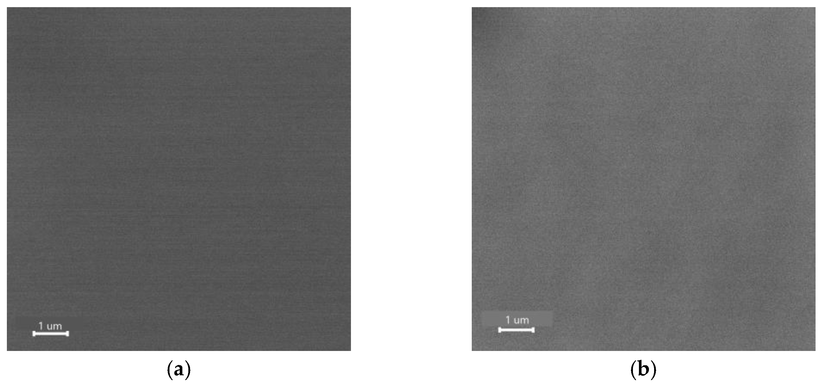
Figure 2.
X-ray diffraction (XRD) spectrum of (a) InSe (b) Sb2Se3.
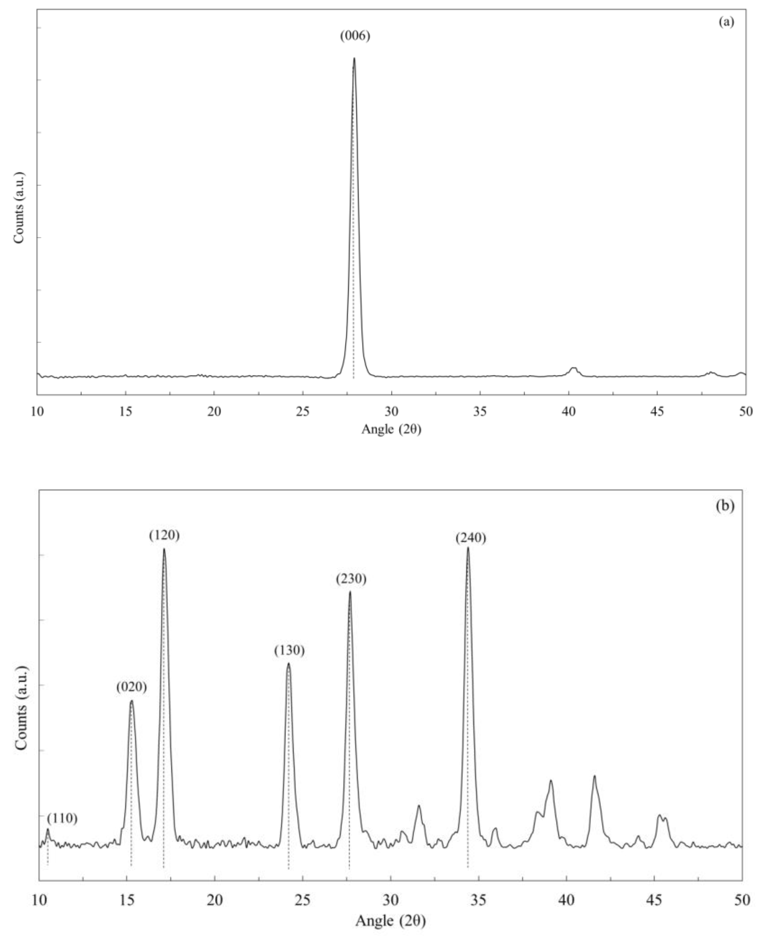
Figure 3.
Raman spectrograph of (a) γ-InSe (b) Sb2Se3.
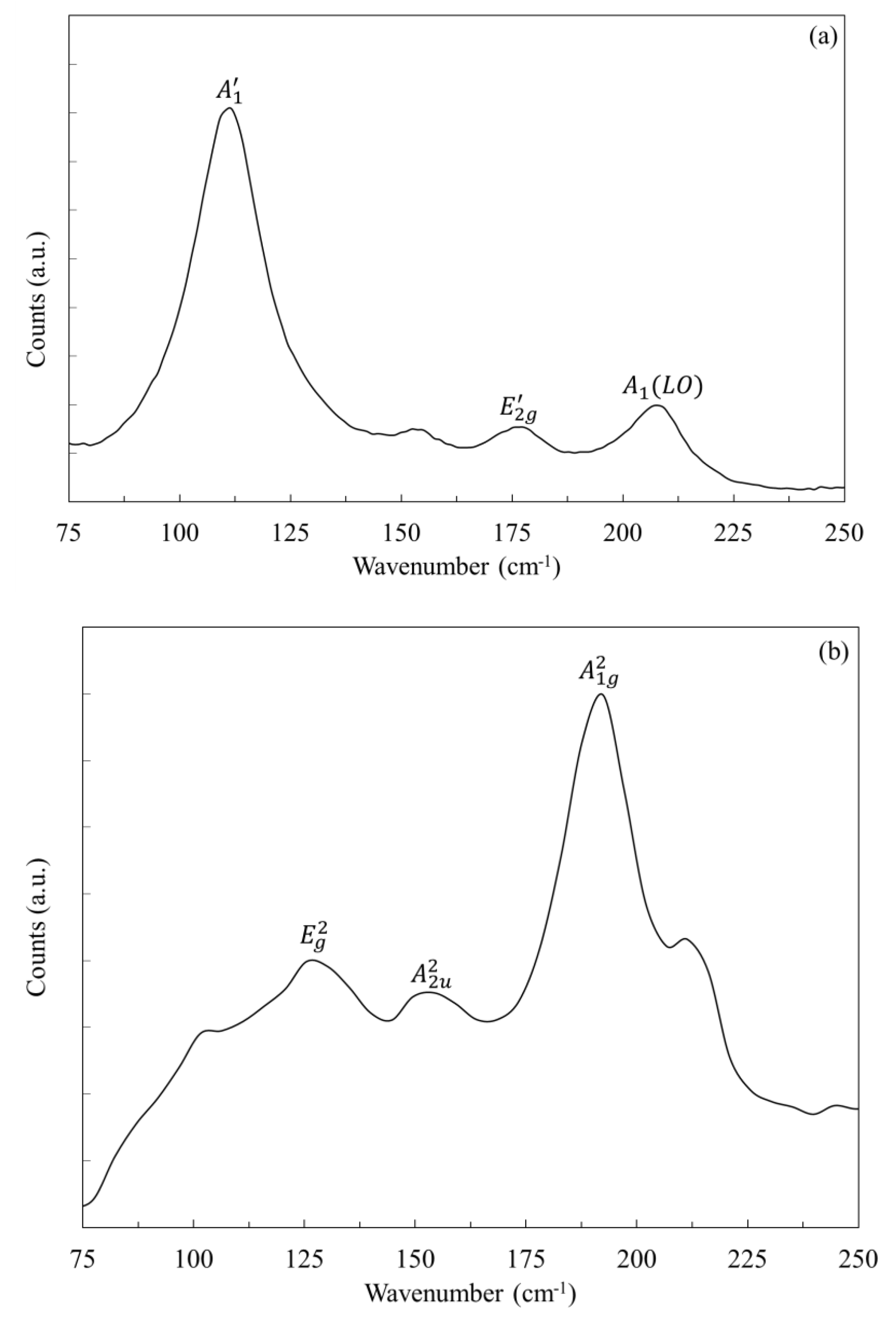
Figure 4.
Absorbance spectrum of (a) InSe (b) Sb2Se3.
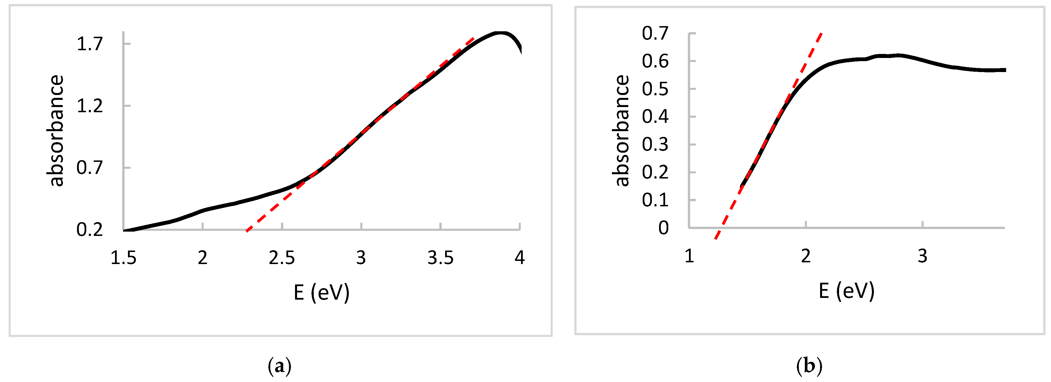
Figure 5.
X-ray photoelectron spectroscopy (XPS) profile of (a) In (b) Se.

Figure 6.
XPS profile of (a) Sb (b) Se.

Figure 7.
Current–voltage (I–V) profile of the InSe/Sb2Se3 pn junction.
© 2017 by the authors. Licensee MDPI, Basel, Switzerland. This article is an open access article distributed under the terms and conditions of the Creative Commons Attribution (CC BY) license (http://creativecommons.org/licenses/by/4.0/).
Share and Cite
MDPI and ACS Style
Browning, R.; Kuperman, N.; Moon, B.; Solanki, R. Atomic Layer Growth of InSe and Sb2Se3 Layered Semiconductors and Their Heterostructure. Electronics 2017, 6, 27. https://doi.org/10.3390/electronics6020027
AMA Style
Browning R, Kuperman N, Moon B, Solanki R. Atomic Layer Growth of InSe and Sb2Se3 Layered Semiconductors and Their Heterostructure. Electronics. 2017; 6(2):27. https://doi.org/10.3390/electronics6020027
Chicago/Turabian StyleBrowning, Robert, Neal Kuperman, Bill Moon, and Raj Solanki. 2017. "Atomic Layer Growth of InSe and Sb2Se3 Layered Semiconductors and Their Heterostructure" Electronics 6, no. 2: 27. https://doi.org/10.3390/electronics6020027
Note that from the first issue of 2016, this journal uses article numbers instead of page numbers. See further details here.