The Electrical Properties of Plasma-Deposited Thin Films Derived from Pelargonium graveolens

1
Electronics Materials Lab, College of Science and Engineering, James Cook University, Townsville, QLD 4811, Australia
2
School of Chemistry, Physics, Mechanical Engineering, Queensland University of Technology, Brisbane, QLD 4000, Australia
*
Author to whom correspondence should be addressed.
Electronics 2017, 6(4), 86; https://doi.org/10.3390/electronics6040086
Submission received: 20 September 2017
/
Revised: 13 October 2017
/
Accepted: 16 October 2017
/
Published: 18 October 2017
Abstract
:Inherently volatile at atmospheric pressure and room temperature, plant-derived precursors present an interesting human-health-friendly precursor for the chemical vapour deposition of thin films. The electrical properties of films derived from Pelargonium graveolens (geranium) were investigated in metal–insulator–metal (MIM) structures. Thin polymer-like films were deposited using plasma-enhanced synthesis under various plasma input power. The J–V characteristics of thus-fabricated MIM were then studied in order to determine the direct current (DC) conduction mechanism of the plasma polymer layers. It was found that the capacitance of the plasma-deposited films decreases at low frequencies (C ≈ 10−11) and remains at a relatively constant value (C ≈ 10−10) at high frequencies. These films also have a low dielectric constant across a wide range of frequencies that decreases as the input RF power increases. The conductivity was determined to be around 10−16–10−17 Ω−1 m−1, which is typical for insulating materials. The Richardson–Schottky mechanism might dominate charge transport in the higher field region for geranium thin films.
1. Introduction
Polymer thin films gained broad research interest in paving the way for low-cost engineering of large-area flexible electronic devices. Among different polymers investigated for organic electronics, conducting polymers are used as electrodes and contacts for charge transporting [1], semiconducting polymers are employed as active layers in organic thin film transistors (OTFTs) [2] and organic photovoltaics (OPVs) [3], and insulating polymers are used as dielectric layers in OTFTs [4]. Over the years, much attention has been paid to the development of insulating polymers to replace the conventional gate dielectric materials, mostly silicon dioxide (k ~ 4), to realise flexible thin film transistors (TFTs) with a low operating voltage and high mobility [5,6]. To this end, a number of low dielectric constant polymers, such as polystyrene (k ~ 2.6) and polymethyl methacrylate (k ~ 3.5), and high dielectric constant polymers, such as poly (vinyl phenol) (k ~ 4.2) and poly (vinyl alcohol) (k ~ 7.8), have been synthetized and tested [5]. The majority of these polymers exhibit a low dielectric constant; a thicker layer (>300 nm) is hence required to suppress the leakage current. On the other hand, low dielectric thickness is an essential requirement for the gate dielectric to increase the capacitance per unit area and to achieve low operating voltage [7,8]. Unfortunately, reducing the thickness of polymer thin films below 50 nm is extremely challenging because of the formation of pinholes, non-uniformity, and the degradation of the dielectric strength that necessitates higher dielectric constant polymers [5,8,9,10]. Additionally, the present methods for the integration of polymer thin films into devices are mostly solution-assisted and thus present additional challenges, such as the incomplete removal of solvent residues, the degradation of existing layers while in contact with solvents, and a difficulty in achieving local patterning [11]. Therefore, development of polymeric materials with moderate k and stable dielectric performances within a lower thickness range via low-cost techniques compatible with modern microelectronics processing has become important.
Plasma polymerisation is one of the swiftly advancing techniques for fabricating highly uniform, ultra-thin pinhole-free polymer thin films from virtually any monomer on a wide variety of substrates. Where previously it was mostly used to fabricate highly crosslinked polymer-like materials that lacked a regularly repeating structure of conventional polymers [12], recent advances, such as the development of pulsed plasma deposition, have enabled the use of the plasma environment as an initiator and catalyst of chemical polymerisation reactions, producing polymers with a lower degree of cross-linking and a well-defined chemical structure [13,14]. In general, plasma polymers that are used as insulating layers are highly cross-linked, are well-adhered to the substrate, and can be made very thin, with a thickness of few tens of nanometres and with excellent conformity [15]. One of the properties that plasma polymers are recognised for is their high dielectric constant, which enables their application as flexible insulating layers in thin film device structures [16,17]. TFTs that are incorporated with dielectric layers formed by plasma polymerising styrene and vinyl acetate [18], acetylene [19], hexamethyldisiloxane [20], methyl methacrylate (pp-MMA) [21], dichlorotetra-methyldisiloxane (pp-DCTMDS) [17], and allyl amine/vinyl acetic acid [22] have shown good device characteristics. Plasma polymers are also noticed for their excellent surface characteristics, so they are frequently uses as buffer layers to improve the interfacial characteristics in TFTs and organic light-emitting diode (OLED) devices [23,24].
Foreseeing the significant demand, along with the development of novel polymeric materials, much attention has also been paid to sustainable production of these materials from natural precursors. The green synthesis of polymers can markedly reduce the growing environmental concerns raised by the e-wastes (plastics, silicon etc.) and minimizes the dependence of organic electronic industry to petrochemical resources [25]. Furthermore, bio-degradability and biocompatibility of these classes of polymers open up new possibilities, such as the integration of electronics into living tissues [26,27]. Cellulose, hemicellulose, lignin, natural silk, gelatin, shellac, egg albumin, etc. are typical examples of naturally derived compounds that have been proven to be promising for bio-electronics applications [25,26]. Yet the major challenge is to identify a cheap and abundant material and an appropriate method to transform them into polymers, ensuring a low cost, complementary properties, and a better life-cycle assessment [28]. In this regard, plasma-assisted deposition gained considerable interest as plasma provides a highly reactive environment that enables the simple and efficient conversion of bio-renewable resources into diverse structures from simple polymers to advanced carbon nanostructures [29,30,31,32]. Our previous studies showed that essential oils (mixtures of volatile organic molecules extracted from different parts of plants) are promising precursor candidate for plasma polymerisation [29,33,34]. Plasma polymers derived from essential oils such as terpenol, linalyl acetate, and γ-terpinene have been demonstrated to be suitable for different applications such as insulating layers, encapsulation layers in organic electronics, and biocompatible coatings for implants [23,35,36,37].
Hence, plasma polymers fabricated from individual components of essential oils have the potential to meet the various material demands put forward by the organic electronics industry. Material costs, processing complexity, and environmental impact can be further reduced by fabricating polymers directly from multicomponent essential oil instead of pure, individual components (e.g., terpinene-4-ol). However, the properties of essential-oil-derived plasma polymers are correlated with the chemical composition of the precursor oil [38]. For instance, plasma polymer synthesised from terpenol has exhibited electron-blocking hole-transporting behaviour, whereas plasma-polymerised linalyl acetate has not [39]. It is therefore important to further investigate the extent to which the multi-component nature of the oil, in this study the Pelargonium graveolens (geranium essential oil), affects the electrical properties, such as the dielectric constant and conductivity, of the polymer thin films synthesized under varied input RF power.
2. Experimental
Microscope glass slides (76 mm × 26 mm) were sonicated in a solution of distilled water and commercial decon for 20 min before being rinsed in acetone and dried using compressed air. Aluminium electrodes were deposited onto the glass slides using thermal evaporation system model HIND 12A4D (HINDHIVAC, Bangalore, India) under a pressure of 7 × 10⁻⁵ torr. Organic thin layers were fabricated on the aluminium utilising custom-built plasma-enhanced chemical vapor deposition (PECVD) system (MKS Instruments, Andover, MA, USA). A generator provided radio frequency (RF) power at 13.56 MHz to a glass tube via capacitively coupled copper electrodes. The pelargonium essential oil was obtained from Australian Botanical Products, and was used without further modification. The main compounds include citronellol (32%), geraniol (15%), linalool (6%), isomenthone (6%), geranyl formate (2.5%), tiglate (2%), citronellyl formate (6%), guaia-6,9-diene, and 10-epi-γ eudesmol (5%). The chemical structure of some components of pelargonium is presented in Figure 1.
In each experiment, 0.5 g of the monomer was used, producing an average flow rate of ~16 cm3/min and a film thickness in a range ~500–700 nm. Power levels of 10 W, 25 W, 50 W, 75 W, and 100 W were applied to fabricate the organic films. Finally, aluminium electrodes were fabricated on top of the organic layers using a custom made shadow mask, which created a device with metal–insulator–metal (MIM) structures as seen in Figure 2.
Then, dielectric properties were investigated between frequencies of 10 Hz and 100 KHz utilizing a Hioki 3522 LCR meter (Hioki, Ueda, Japan). From the known thickness and the area of the device, and measured C values, dielectric constant was determined. Additionally, I–V measurements were performed on the MIM structures using a Keithley 2636A source meter (Keithley, Cleveland, OH, USA). Data were acquired between 0 and 20 V, with steps of 0.2 V for each point at room temperature.
3. Results and Discussion
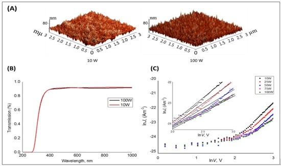
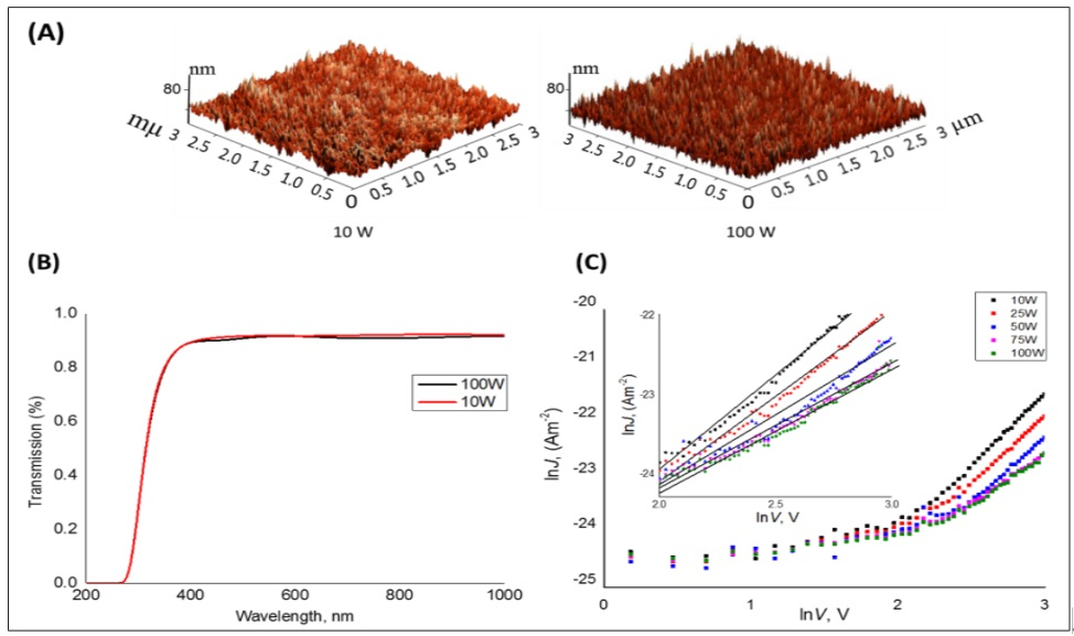
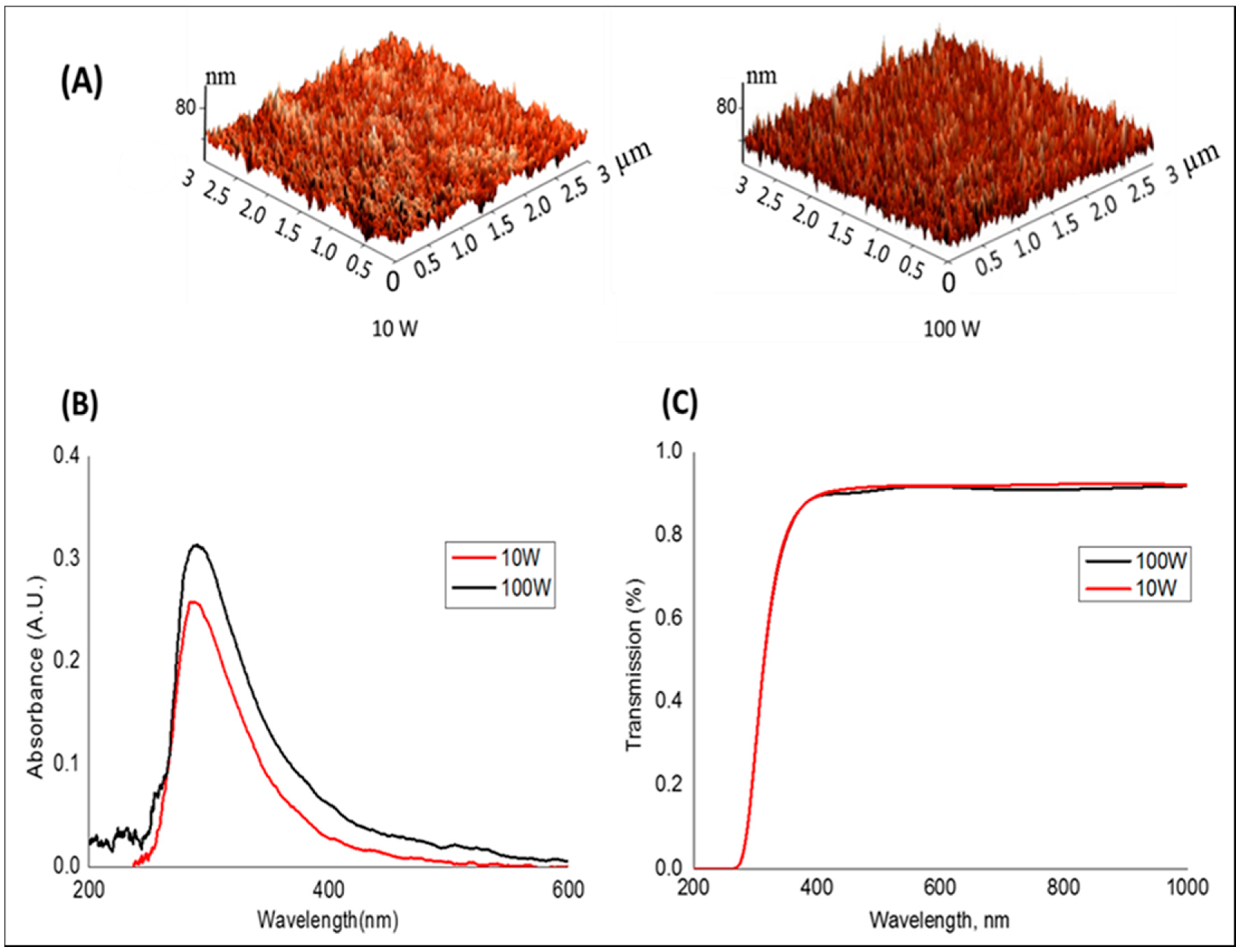
As seen in the atomic force microscopy (AFM) images in Figure 3A, the Pelargonium graveolens plasma polymer films seemed to be smooth, defect-free, and homogeneous on the nano-scale, indicating that polymerisation reactions took place basically on the surface of the substrate instead of in the gas phase. The films were also shown to be optically transparent within the visible wavelength range, based on the absorbance and transmission data in Figure 3B,C, similar to films from γ-terpinene [40] and terpinene-4-ol [38]. Furthermore, the energy gap (Eg) of the pelargonium films was calculated by applying the Tauc relation to the optical absorption coefficient data recorded from UV-Vis spectroscopy measurements. Polymers fabricated at 10 and 100 W had Eg ≈ 3.67 and 3.60 eV, respectively. The reduction in Eg as a result of power deposition was attributed to dangling bonds that formed in the polymer structure during the fabrication process. At low input power density, a low concentration of dangling bonds are created due to their saturation with hydrogen atoms, whereas higher input power enhances the fragmentation rate in the plasma field [41], which highly accelerates the formation of chains with unsaturated bonds [42]. The relatively high energy gap for geranium plasma polymer films is in good agreement with the low conductivity values acquired in this study. Further details regarding the effect of deposition power on morphological, optical, mechanical, and chemical properties of pelargonium plasma polymer films can be found in [43].
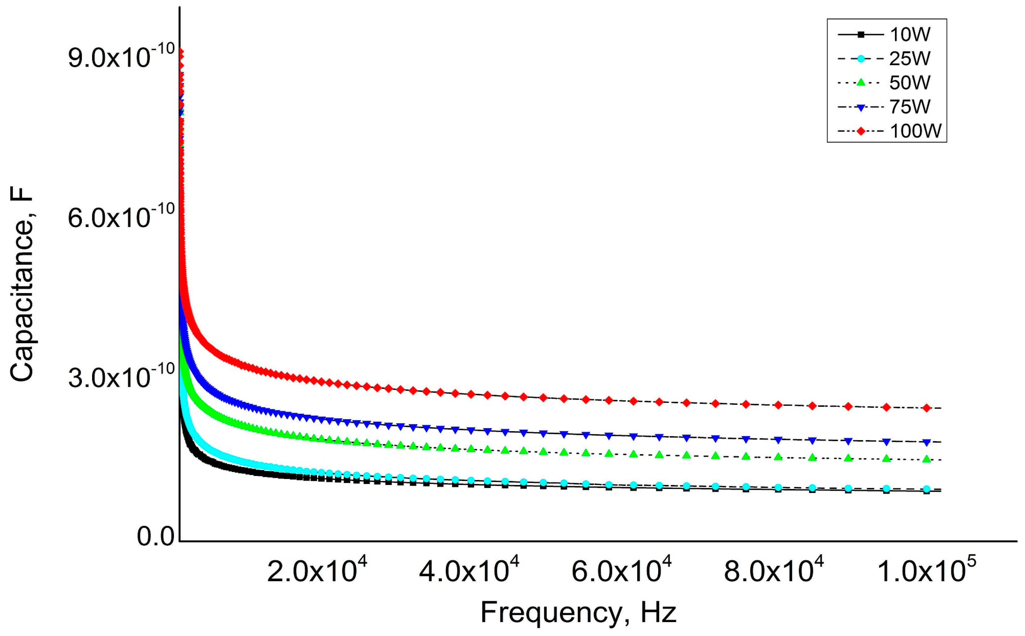
In order to determine the electric behavior of pelargonium plasma polymer films, capacitance data, shown in Figure 4, were acquired using LCR records across frequencies from 10 Hz to 100 KHz. It is clear that the capacitance initially decreases at low frequencies (C ≈ 10−11), approaching a constant value (C ≈ 10−10) at high frequencies for all measured samples. Independent of frequency, deposition power had a slight influence on the capacitance of pelargonium plasma polymer films. Then, based on capacitance values, the dielectric properties (ε) of the polymers were attained and are given in Table 1 as a function of frequency. The dielectric constant value of pelargonium plasma polymer thin films ostensibly decreased as input deposition power increased. This decrease can be associated with the increase in carbon and reduction in oxygen content in the films’ structure with RF power [36]. In addition, it was documented that higher input powers increase the degree of cross-linking that render the polymer more dense, reducing the dielectric property and leakage current density [44].
Independent of deposition power, all of the samples have approximately the same frequency dependence of the dielectric constant, which noticeably decreases at initial low frequencies. In dielectric materials, there are some trapped charges that can typically move for a short distance through the material once an external electric field is applied [45]. These carriers can cause space charges and macroscopic field distortions when they are impeded in their motion. It is known that when charge carriers migrate under the impact of an electric field, they most likely become blocked at the electrode–dielectric interface, which causes interfacial polarisation [45,46]. The interfacial polarisation phenomena are characteristically observed in sandwich-type configurations, where they lead to an increase in capacitance of the polymer at low frequencies [47]. This may be one of the explanations for the high value of the dielectric constants experimentally observed in the pelargonium films within the low frequency region. On the other hand, at higher frequencies, interfacial polarisation effects are significantly less dominant and do not have an important influence on dielectric constant values [44]. The dielectric constant for all polymers gradually decreases at higher frequencies, showing behavioural characteristics of a polymer insulating material.
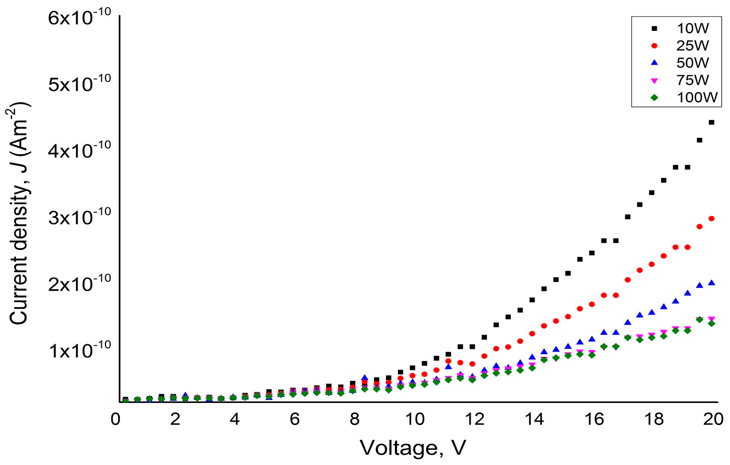
The charge transport mechanism in pelargonium plasma polymer films was investigated through standard current–voltage characterisation in the voltage range of 0.1–20 V. The three main transport mechanisms typically observed in organic films are Richardson–Schottky (RS) conduction, Poole–Frenkel (PF) conduction, and space-charge-limited conduction (SCLC). The PF mechanism refers to a bulk-limited conduction route in which the trap barrier of the material is dropped by the application of an adequately high electric field [35]. The RS conduction designates a barrier-limited conduction route, in which there is an interaction of an electric field at a metal–insulator edge that prompts a dropping of the potential barrier [48]. SCLC is a mechanism where the current conducted through the solid material is limited by a distribution of traps in the bulk material [36]. Theoretically, a linear dependence of ln J−lnV indicates a possibility of a SCLC mechanism, while a linear dependence of ln J−V1/2 points toward a predominance of RS or PF conduction [49]. In the low field region, various mechanisms most likely govern the conduction process of the polymer, whereas, at higher fields, one mechanism starts to dominate [35].
The physical relationship between the current density (J) in an insulator and the applied voltage (V) at a temperature T is given by the following mathematical formula [36,50]:
where J0 is the low field current density, V is the voltage, T is the absolute temperature, kB is Boltzmann’s constant, and d is the film thickness. The parameter β is the field dropping coefficient and for PF and RS conduction mechanisms is given by βPF and βRS, respectively [51], expressed as follows:
where q is the electronic charge, ε0 is the free space permittivity, and εr is the dielectric constant.
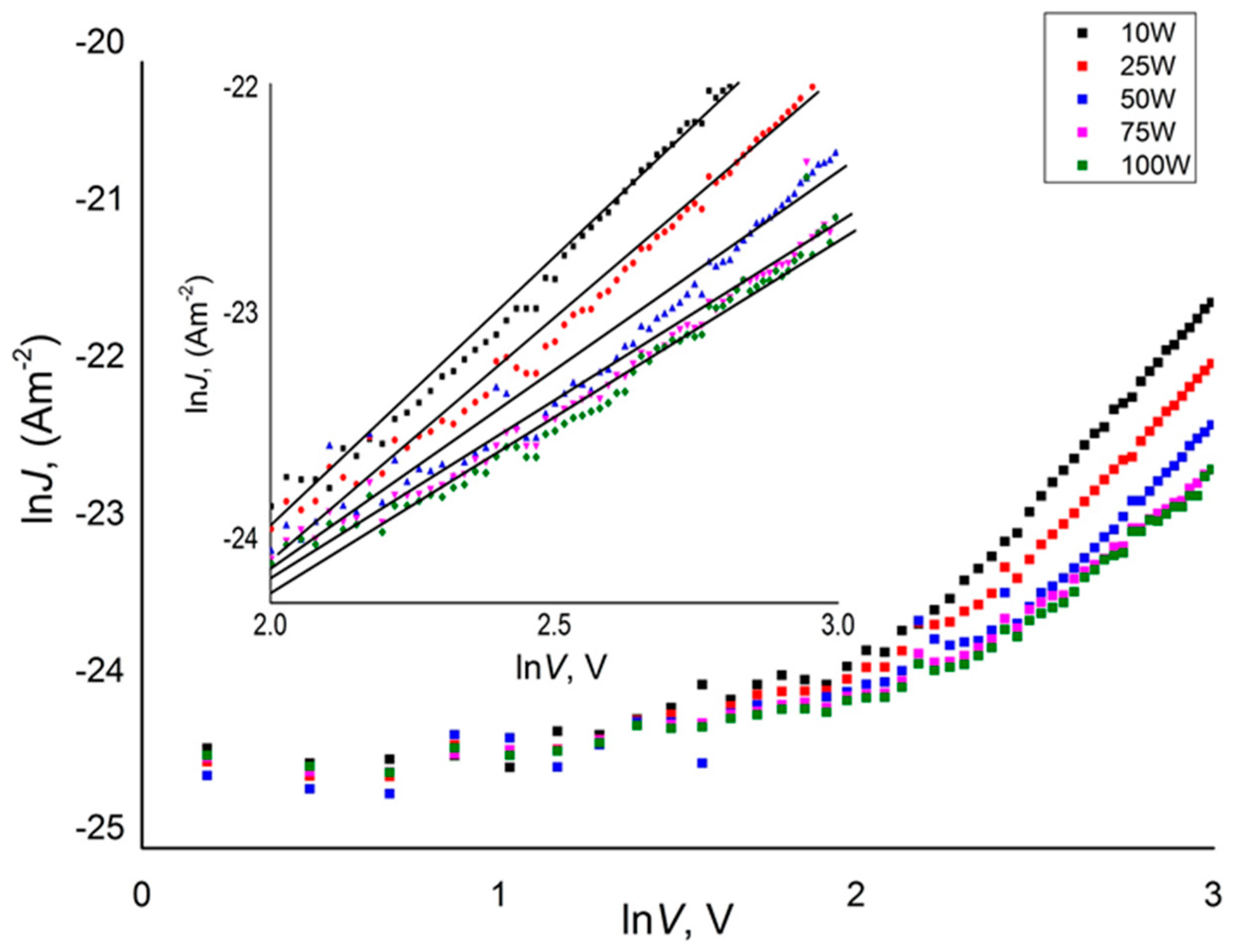
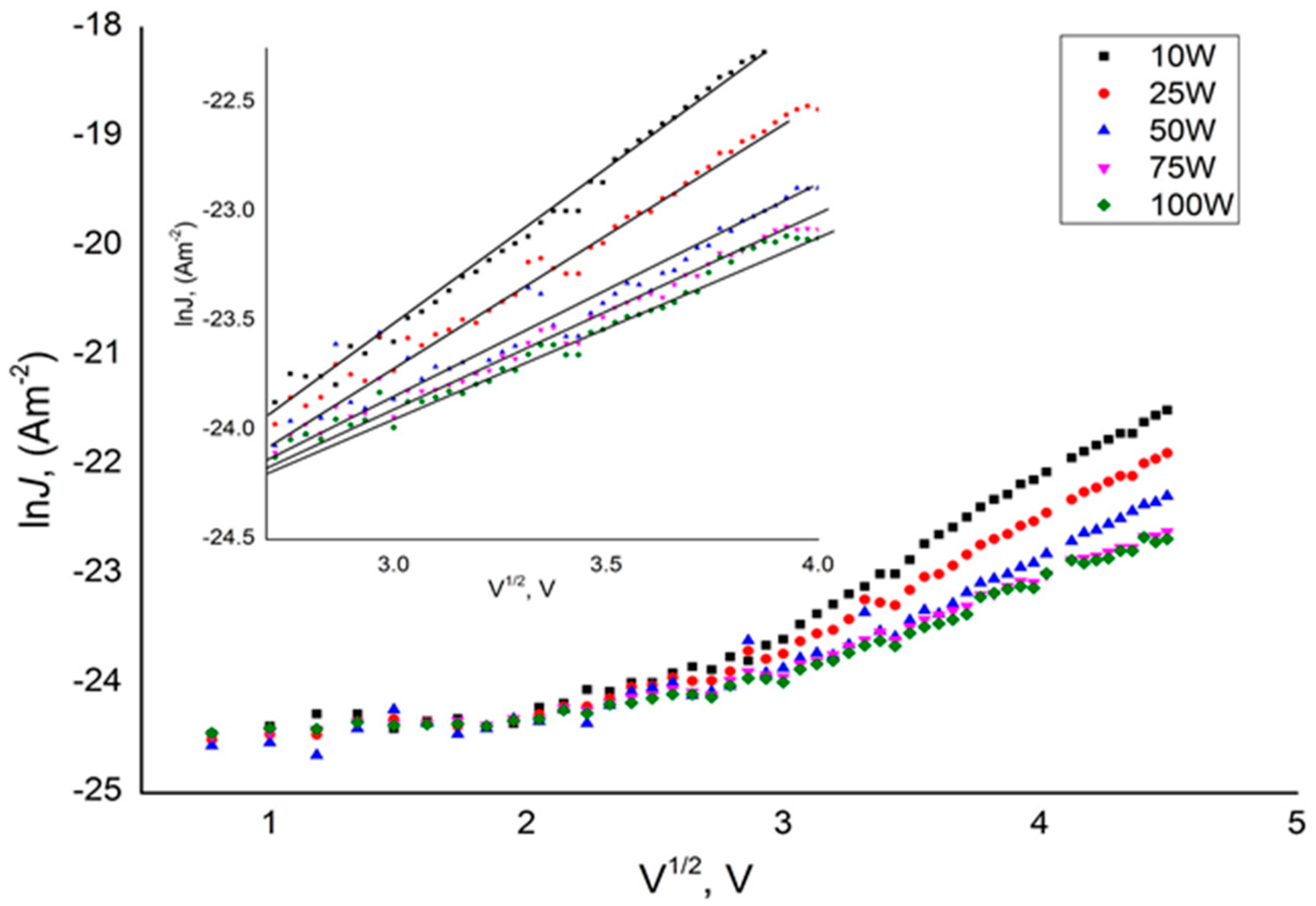
The relation between the current density of pelargonium plasma polymer films with an applied voltage of 0–20 V is given in Figure 5. The J–V characteristic can be expressed by a power law relation J ∝ Vn, where n is a power law index. In the low field region (0–3 V), the value of n for all pelargonium films is found to be within the range of 0.4 < n < 0.6. Further, the plots of lnJ vs. V1/2 with an applied voltage in Figure 6 show that the current density J displays an almost ohmic dependence on the applied voltage in the low region. Whereas in the higher field region (3–20 V), the value of n is considerably increased, ranging within 2.1 < n < 3.3, and ln J is straight to V1/2, indicating a non-ohmic charge transport process. In addition, the fitting of ln J vs. lnV for all pelargonium plasma polymer films in Figure 7 demonstrate similar behaviour as those in Figure 6. According to power law index values and the linear fitting of the J–V plots, RS or PF conduction mechanisms are expected for geranium thin films.
In order to distinguish between PF and RS mechanisms, theoretical parameters (βS and βPF) and experimental βexp should be determined. The following relation was used to estimate βexp [35]:
Using the dielectric value acquired at high frequencies, both βS and βPF were calculated as ~2.2 × 10⁻⁵ eV·m1/2·V−1/2 and 4.4 × 10⁻⁵ eV·m1/2·V−1/2, respectively, and summarised in Table 2. Likewise, the coefficient βexp were determined to be around 2.5 × 10⁻⁵ eV·m1/2·V−1/2. Hence, by comparing βS and βPF with the βexp coefficient, the Schottky mechanism might dominate the charge transport of pelargonium plasma polymer films in the higher field region.
The current–voltage characterisation was then used to estimate the dc conductivity (σ) of the polymerised films through the following relation:
where d is the thickness of the material, J is the measured current density, and V is the applied voltage. Independent of the power of deposition, the maximum conductivity for all samples was found to be in the range of 10−16–10−17 Ω−1·m−1, which is a typical value for insulators. The deposition power slightly reduced the conductivity value, which can be ascribed to the more amorphous nature of the films deposited at higher power densities [35]. It is important to mention that the difference in the conductivity could not be solely related to structural changes induced by the plasma power. If the SCLC mechanism is responsible for the observed behaviour of the polymer, thickness dependent conductivity may appear as well. However, the conductivity of the plasma-polymer-derived films was significantly lower than that of other known amorphous polymers fabricated using plasma. Generally, plasma polymers derived from essential oil such as cis-β-ocimene, γ-terpinene, and linalyl acetate have conductivities in the range of 10−12–10−11 Ω−1·m−1 [35,52,53].
4. Conclusions
The electrical properties of thin films derived from plasma-polymerised Pelargonium graveolens (geranium) were studied across frequencies of 10 Hz to 100 KHz in metal–insulator–metal (MIM) structures for several plasma input powers. The dielectric constant was observed to decrease with increasing deposition power, which can be attributed to the increase in carbon rate and the reduction in oxygen content in the formed films. Regardless of the input power, all investigated samples have approximately the same frequency dependence on the dielectric constant, where it rapidly decreases within a low frequency region. Furthermore, the charge transport mechanism was investigated through a standard current–voltage characterisation, showing that the Schottky mechanism might be the dominant mechanism in the higher field region. These polymers revealed a relatively low conductivity value (10−16–10−17 Ω−1 m−1), demonstrating characteristics of a typical insulator material. The aforementioned properties, in addition to other advantageous characteristics of geranium plasma polymer thin films (e.g., low density, high adhesion to substrates, relatively high optical band gap, and uniform coverage), render them a suitable candidate for various dielectric applications in advanced microelectronics.
Acknowledgments
A.A.-J. is grateful to the Ministry of Higher Education and Scientific Research, Iraq and JCUPRS for the financial support.
Author Contributions
A.A.-J. and S.A. fabricated the polymerized films, obtained thin film characteristics, interpreted and analyzed the data and write the manuscript. K.B. assisted in the interpretation the results of this manuscript. M.V.J. coordinated and managed the experimental work and guided the overall preparation of the manuscript.
Conflicts of Interest
The authors declare no conflict of interest.
References
- Yim, J.H.; Joe, S.-Y.; Pang, C.; Lee, K.M.; Jeong, H.; Park, J.-Y.; Ahn, Y.H.; de Mello, J.C.; Lee, S. Fully solution-processed semitransparent organic solar cells with a silver nanowire cathode and a conducting polymer anode. ACS Nano 2014, 8, 2857–2863. [Google Scholar] [CrossRef] [PubMed]
- Tseng, H.R.; Phan, H.; Luo, C.; Wang, M.; Perez, L.A.; Patel, S.N.; Ying, L.; Kramer, E.J.; Nguyen, T.Q.; Bazan, G.C.; et al. High-Mobility Field-Effect Transistors Fabricated with Macroscopic Aligned Semiconducting Polymers. Adv. Mater. 2014, 26, 2993–2998. [Google Scholar] [CrossRef] [PubMed]
- He, Z.; Xiao, B.; Liu, F.; Wu, H.; Yang, Y.; Xiao, S.; Wang, C.; Russell, T.P.; Cao, Y. Single-junction polymer solar cells with high efficiency and photovoltage. Nat. Photonics 2015, 9, 174–179. [Google Scholar] [CrossRef]
- Moon, H.; Seong, H.; Shin, W.C.; Park, W.-T.; Kim, M.; Lee, S.; Bong, J.H.; Noh, Y.-Y.; Cho, B.J.; Yoo, S.; et al. Synthesis of ultrathin polymer insulating layers by initiated chemical vapour deposition for low-power soft electronics. Nat. Mater. 2015, 14, 628–635. [Google Scholar] [CrossRef] [PubMed]
- Ortiz, R.P.; Facchetti, A.; Marks, T.J. High-k organic, inorganic, and hybrid dielectrics for low-voltage organic field-effect transistors. Chem. Rev. 2009, 110, 205–239. [Google Scholar] [CrossRef] [PubMed]
- Kumar, B.; Kaushik, B.K.; Negi, Y. Perspectives and challenges for organic thin film transistors: Materials, devices, processes and applications. J. Mater. Sci. Mater. Electron. 2014, 25, 1–30. [Google Scholar] [CrossRef]
- Liu, X.; Guo, Y.; Ma, Y.; Chen, H.; Mao, Z.; Wang, H.; Yu, G.; Liu, Y. Flexible, Low-Voltage and High-Performance Polymer Thin-Film Transistors and Their Application in Photo/Thermal Detectors. Adv. Mater. 2014, 26, 3631–3636. [Google Scholar] [CrossRef] [PubMed]
- Choi, J.; Joo, M.; Seong, H.; Pak, K.; Park, H.; Park, C.W.; Im, S.G. Flexible, Low-Power Thin-Film Transistors (TFTs) Made of Vapor-Phase Synthesized High-k, Ultrathin Polymer Gate Dielectrics. ACS Appl. Mater. Interfaces 2017, 9, 20808–20817. [Google Scholar] [CrossRef] [PubMed]
- Facchetti, A.; Yoon, M.H.; Marks, T.J. Gate Dielectrics for Organic Field-Effect Transistors: New Opportunities for Organic Electronics. Adv. Mater. 2005, 17, 1705–1725. [Google Scholar] [CrossRef]
- Cheng, X.; Caironi, M.; Noh, Y.-Y.; Wang, J.; Newman, C.; Yan, H.; Facchetti, A.; Sirringhaus, H. Air stable cross-linked Cytop ultrathin gate dielectric for high yield low-voltage top-gate organic field-effect transistors. Chem. Mater. 2010, 22, 1559–1566. [Google Scholar] [CrossRef]
- Eslamian, M. Inorganic and organic solution-processed thin film devices. Nano-Micro Lett. 2017, 9, 3. [Google Scholar] [CrossRef]
- Friedrich, J. Mechanisms of Plasma Polymerization—Reviewed from a Chemical Point of View. Plasma Process. Polym. 2011, 8, 783–802. [Google Scholar] [CrossRef]
- Boscher, N.D.; Hilt, F.; Duday, D.; Frache, G.; Fouquet, T.; Choquet, P. Atmospheric Pressure Plasma Initiated Chemical Vapor Deposition Using Ultra-Short Square Pulse Dielectric Barrier Discharge. Plasma Process. Polym. 2015, 12, 66–74. [Google Scholar] [CrossRef]
- Hilt, F.; Duday, D.; Gherardi, N.; Frache, G.; Didierjean, J.; Choquet, P. Plasma polymerisation of an allyl organophosphate monomer by atmospheric pressure pulsed-PECVD: Insights into the growth mechanisms. RSC Adv. 2015, 5, 4277–4285. [Google Scholar] [CrossRef]
- Flamm, D.L.; Auciello, O. Plasma Deposition, Treatment, and Etching of Polymers: The Treatment and Etching of Polymers; d’Agostino, R., Ed.; Academic Press: San Diego, CA, USA, 2012. [Google Scholar]
- Bhattacharyya, D.; Yoon, W.-J.; Berger, P.R.; Timmons, R.B. Plasma-Polymerized Multistacked Organic Bipolar Films: A New Approach to Flexible High-κ Dielectrics. Adv. Mater. 2008, 20, 2383–2388. [Google Scholar] [CrossRef]
- Xu, Y.; Berger, P.R. Pulsed plasma polymerized dichlorotetramethyldisiloxane high-k gate dielectrics for polymer field-effect transistors. J. Appl. Phys. 2006, 99, 014104. [Google Scholar] [CrossRef]
- Lim, J.-S.; Shin, P.-K.; Lee, B.-J. Organic Thin Film Transistors with Gate Dielectrics of Plasma Polymerized Styrene and Vinyl Acetate Thin Films. Trans. Electric. Electron. Mater. 2015, 16, 95–98. [Google Scholar] [CrossRef]
- Feng, L.; Anguita, J.V.; Tang, W.; Zhao, J.; Guo, X.; Silva, S.R.P. Room Temperature Grown High-Quality Polymer-Like Carbon Gate Dielectric for Organic Thin-Film Transistors. Adv. Electron. Mater. 2016, 2, 1500374. [Google Scholar] [CrossRef]
- Tsai, C.H.; Li, Y.-S.; Cheng, I.-C.; Chen, J.-Z. O2/HMDSO-Plasma-Deposited Organic–Inorganic Hybrid Film for Gate Dielectric of MgZnO Thin-Film Transistor. Plasma Process. Polym. 2014, 11, 89–95. [Google Scholar] [CrossRef]
- Lim, J.-S.; Shin, P.-K.; Lee, B.-J.; Lee, S. Plasma polymerized methyl methacrylate gate dielectric for organic thin-film transistors. Org. Electron. 2010, 11, 951–954. [Google Scholar] [CrossRef]
- Yoon, W.-J.; Bhattacharyya, D.; Timmons, R.B.; Berger, P.R. Plasma-polymerized multistacked bipolar gate dielectric for organic thin-film transistors. Org. Electron. 2010, 11, 1767–1771. [Google Scholar] [CrossRef]
- Jacob, M.V.; Bazaka, K.; Weis, M.; Taguchi, D.; Manaka, T.; Iwamoto, M. Fabrication and characterization of polyterpenol as an insulating layer and incorporated organic field effect transistor. Thin Solid Films 2010, 518, 6123–6129. [Google Scholar] [CrossRef]
- Kwok, H.S.; Wong, M.; Peng, H.; Sun, J. Metallic Anode Treated by Carbon Tetrafluoride Plasma for Organic Light Emitting Device. U.S. Patent 9,166,197 B2, 20 October 2015. [Google Scholar]
- Zhu, H.; Luo, W.; Ciesielski, P.N.; Fang, Z.; Zhu, J.Y.; Henriksson, G.; Himmel, M.E.; Hu, L. Wood-derived materials for green electronics, biological devices, and energy applications. Chem. Rev. 2016, 116, 9305–9374. [Google Scholar] [CrossRef] [PubMed]
- Irimia-Vladu, M. “Green” electronics: Biodegradable and biocompatible materials and devices for sustainable future. Chem. Soc. Rev. 2014, 43, 588–610. [Google Scholar] [CrossRef] [PubMed]
- Irimia-Vladu, M.; Głowacki, E.; Voss, G.; Bauer, S.; Sariciftci, N.S. Green and biodegradable electronics. Mater. Today 2012, 15, 340–346. [Google Scholar] [CrossRef]
- Zhu, Y.; Romain, C.; Williams, C.K. Sustainable polymers from renewable resources. Nature 2016, 540, 354–362. [Google Scholar] [CrossRef] [PubMed]
- Bazaka, K.; Jacob, M. Synthesis of radio frequency plasma polymerized non-synthetic Terpinen-4-ol thin films. Mater. Lett. 2009, 63, 1594–1597. [Google Scholar] [CrossRef]
- Jacob, M.V.; Rawat, R.S.; Ouyang, B.; Bazaka, K.; Kumar, D.S.; Taguchi, D.; Iwamoto, M.; Neupane, R.; Varghese, O.K. Catalyst-free plasma enhanced growth of graphene from sustainable sources. Nano Lett. 2015, 15, 5702–5708. [Google Scholar] [CrossRef] [PubMed]
- Bazaka, K.; Jacob, M.V.; Ostrikov, K. Sustainable Life Cycles of Natural-Precursor-Derived Nanocarbons. Chem. Rev. 2016, 116, 163–214. [Google Scholar] [CrossRef] [PubMed] [Green Version]
- Al-Jumaili, A.; Alancherry, S.; Bazaka, K.; Jacob, M.V. Review on the antimicrobial properties of carbon nanostructures. Materials 2017, 10, 1066. [Google Scholar] [CrossRef] [PubMed]
- Jacob, M.V.; Easton, C.D.; Woods, G.S.; Berndt, C.C. Fabrication of a novel organic polymer thin film. Thin Solid Films 2008, 516, 3884–3887. [Google Scholar] [CrossRef]
- Anderson, L.; Jacob, M. Effect of RF power on the optical and morphological properties of RF plasma polymerised linalyl acetate thin films. Appl. Surf. Sci. 2010, 256, 3293–3298. [Google Scholar] [CrossRef]
- Anderson, L.; Jacob, M. Electrical characterisations of plasma polyermised linalyl acetate. Mater. Sci. Eng. B 2012, 177, 311–315. [Google Scholar] [CrossRef]
- Ahmad, J.; Bazaka, K.; Vasilev, K.; Jacob, M.V. Electrical conduction in plasma polymerized thin films of γ-terpinene. J. Appl. Polym. Sci. 2015, 132. [Google Scholar] [CrossRef] [Green Version]
- Bazaka, K.; Jacob, M.V.; Crawford, R.J.; Ivanova, E.P. Plasma-assisted surface modification of organic biopolymers to prevent bacterial attachment. Acta Biomater. 2011, 7, 2015–2028. [Google Scholar] [CrossRef] [PubMed]
- Bazaka, K.; Jacob, M.V.; Bowden, B.F. Optical and chemical properties of polyterpenol thin films deposited via plasma-enhanced chemical vapor deposition. J. Mater. Res. 2011, 26, 1018–1025. [Google Scholar] [CrossRef] [Green Version]
- Jacob, M.V.; Bazaka, K.; Taguchi, D.; Manaka, T.; Iwamoto, M. Electron-blocking hole-transport polyterpenol thin films. Chem. Phys. Lett. 2012, 528, 26–28. [Google Scholar] [CrossRef] [Green Version]
- Ahmad, J.; Bazaka, K.; Jacob, M.V. Optical and surface characterization of radio frequency plasma polymerized 1-isopropyl-4-methyl-1, 4-cyclohexadiene thin films. Electronics 2014, 3, 266–281. [Google Scholar] [CrossRef] [Green Version]
- Ahmad, J.; Bazaka, K.; Whittle, J.D.; Michelmore, A.; Jacob, M.V. Structural Characterization of γ-Terpinene Thin Films Using Mass Spectroscopy and X-ray Photoelectron Spectroscopy. Plasma Process. Polym. 2015, 12, 1085–1094. [Google Scholar] [CrossRef]
- Vassallo, E.; Cremona, A.; Ghezzi, F.; Laguardia, L.; Ambrosone, G.; Coscia, U. Structural and optical properties of amorphous hydrogenated silicon carbonitride films produced by PECVD. Appl. Surf. Sci. 2006, 252, 7993–8000. [Google Scholar] [CrossRef]
- Al-Jumaili, A.; Bazaka, K.; Jacob, M.V. Retention of Antibacterial Activity in Geranium Plasma Polymer Thin Films. Nanomaterials 2017, 7, 270. [Google Scholar] [CrossRef] [PubMed]
- Bazaka, K.; Destefani, R.; Jacob, M.V. Plant-derived cis-β-ocimene as a precursor for biocompatible, transparent, thermally-stable dielectric and encapsulating layers for organic electronics. Sci. Rep. 2016, 6, 38571. [Google Scholar] [CrossRef] [PubMed]
- Kumar, D.S.; Yoshida, Y. Dielectric properties of plasma polymerized pyrrole thin film capacitors. Surf. Coat. Technol. 2003, 169, 600–603. [Google Scholar] [CrossRef]
- Chowdhury, F.-U.-Z.; Bhuiyan, A. Dielectric properties of plasma-polymerized diphenyl thin films. Thin Solid Films 2000, 370, 78–84. [Google Scholar] [CrossRef]
- Mathai, C.J.; Saravanan, S.; Anantharaman, M.R.; Venkitachalam, S.; Jayalekshmi, S. Characterization of low dielectric constant polyaniline thin film synthesized by ac plasma polymerization technique. J. Phys. D Appl. Phys. 2002, 35, 240–245. [Google Scholar] [CrossRef]
- Bazaka, K.; Jacob, M.V. Effects of iodine doping on optoelectronic and chemical properties of polyterpenol thin films. Nanomaterials 2017, 7, 11. [Google Scholar] [CrossRef] [PubMed]
- Matin, R.; Bhuiyan, A. Electrical transport mechanism in plasma polymerized 2, 6, diethylaniline thin films. Thin Solid Films 2011, 519, 3462–3467. [Google Scholar] [CrossRef]
- Dakhel, A. Mechanisms of dc-current transfer in tris (acetylacetonato) iron (III) films. J. Non-Cryst. Solids 2007, 353, 1529–1533. [Google Scholar] [CrossRef]
- Capan, R.; Davis, F. Electrical properties of a calix [4] acid/amine Langmuir–Blodgett thin film. Mater. Chem. Phys. 2011, 125, 883–886. [Google Scholar] [CrossRef]
- Bazaka, K.; Jacob, M.V. Complex permittivity measurements of RF plasma polymerized polyterpenol organic thin films employing split post dielectric resonator. J. Polym. Eng. 2011, 31, 73–75. [Google Scholar] [CrossRef]
- Kiesow, A.; Heilmann, A. Deposition and properties of plasma polymer films made from thiophenes. Thin Solid Films 1999, 343, 338–341. [Google Scholar] [CrossRef]
Figure 1.
The chemical structure of main components of pelargonium essential oil.
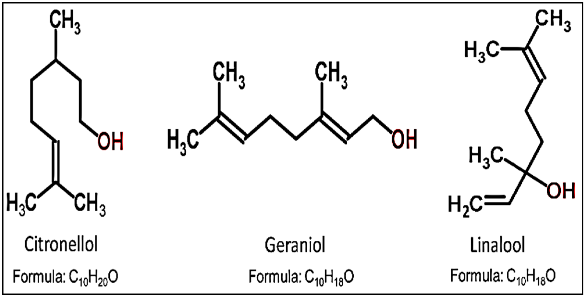
Figure 2.
Metal–insulator–metal (MIM) structure used to study the electrical properties of geranium plasma polymer thin films.
Figure 2.
Metal–insulator–metal (MIM) structure used to study the electrical properties of geranium plasma polymer thin films.

Figure 3.
(A) Atomic force microscope images of pelargonium plasma polymer films fabricated at 10 W and 100 W. (B) Ultraviolet–visible spectroscopy (UV-VIS) measurements of pelargonium plasma polymer films deposited at various input power. (C) Optical transmission of pelargonium plasma polymer films deposited at 10 W and 100 W.

Figure 4.
Capacitance of plasma-polymerised pelargonium thin films fabricated at different deposition power as a function of frequency in the range of 10–100 kHz.
Figure 4.
Capacitance of plasma-polymerised pelargonium thin films fabricated at different deposition power as a function of frequency in the range of 10–100 kHz.

Figure 5.
Current density (J) of pelargonium plasma polymer thin films with an applied voltage (V) between 0 and 20 V.
Figure 5.
Current density (J) of pelargonium plasma polymer thin films with an applied voltage (V) between 0 and 20 V.

Figure 6.
Variation of ln J with square root of applied voltage for pelargonium plasma polymer thin films fabricated at different deposition powers.
Figure 6.
Variation of ln J with square root of applied voltage for pelargonium plasma polymer thin films fabricated at different deposition powers.

Figure 7.
Variation of ln J with lnV for pelargonium plasma polymer thin films fabricated at different deposition powers.
Figure 7.
Variation of ln J with lnV for pelargonium plasma polymer thin films fabricated at different deposition powers.

Table 1.
Variation of the corresponding dielectric constants with frequency for pelargonium plasma polymer thin films in the range of 10–100 kHz.
Table 1.
Variation of the corresponding dielectric constants with frequency for pelargonium plasma polymer thin films in the range of 10–100 kHz.
| Frequency (Hz) | Dielectric Constant | ||||
|---|---|---|---|---|---|
| 10 W | 25 W | 50 W | 75 W | 100 W | |
| 10 | 5.75 | 4.92 | 4.74 | 4.62 | 4.29 |
| 100 | 4.73 | 4.10 | 3.38 | 2.97 | 2.56 |
| 500 | 4.48 | 3.88 | 3.03 | 2.62 | 2.20 |
| 1000 | 4.40 | 3.80 | 2.93 | 2.52 | 2.10 |
| 10,000 | 4.17 | 3.59 | 2.66 | 2.26 | 1.85 |
| 50,000 | 3.69 | 3.24 | 2.37 | 1.98 | 1.59 |
| 100,000 | 3.05 | 2.78 | 2.04 | 1.68 | 1.32 |
Table 2.
Experimental βexp and theoretical βPF and βRS values of pelargonium plasma polymer films.
| Power of Deposition (W) | βexp | βPF | βRS |
|---|---|---|---|
| 10 | 2.53 × 10⁻⁵ | 4.32 × 10⁻⁵ | 2.16 × 10⁻⁵ |
| 25 | 2.55 × 10⁻⁵ | 4.40 × 10⁻⁵ | 2.20 × 10⁻⁵ |
| 50 | 2.58 × 10⁻⁵ | 4.42 × 10⁻⁵ | 2.21 × 10⁻⁵ |
| 75 | 2.59 × 10⁻⁵ | 4.45 × 10⁻⁵ | 2.22 × 10⁻⁵ |
| 100 | 2.61 × 10⁻⁵ | 4.46 × 10⁻⁵ | 2.23 × 10⁻⁵ |
© 2017 by the authors. Licensee MDPI, Basel, Switzerland. This article is an open access article distributed under the terms and conditions of the Creative Commons Attribution (CC BY) license (http://creativecommons.org/licenses/by/4.0/).
Share and Cite
MDPI and ACS Style
Al-Jumaili, A.; Alancherry, S.; Bazaka, K.; Jacob, M.V. The Electrical Properties of Plasma-Deposited Thin Films Derived from Pelargonium graveolens. Electronics 2017, 6, 86. https://doi.org/10.3390/electronics6040086
AMA Style
Al-Jumaili A, Alancherry S, Bazaka K, Jacob MV. The Electrical Properties of Plasma-Deposited Thin Films Derived from Pelargonium graveolens. Electronics. 2017; 6(4):86. https://doi.org/10.3390/electronics6040086
Chicago/Turabian StyleAl-Jumaili, Ahmed, Surjith Alancherry, Kateryna Bazaka, and Mohan V. Jacob. 2017. "The Electrical Properties of Plasma-Deposited Thin Films Derived from Pelargonium graveolens" Electronics 6, no. 4: 86. https://doi.org/10.3390/electronics6040086
Note that from the first issue of 2016, this journal uses article numbers instead of page numbers. See further details here.