Smart E-Beam for Defect Identification & Analysis in the Nanoscale Technology Nodes: Technical Perspectives

1
Synopsys, Mountain View, CA 94043, USA
2
Department of Electrical and Computer Engineering, University of Central Florida, Orlando, FL 32816, USA
*
Author to whom correspondence should be addressed.
Electronics 2017, 6(4), 87; https://doi.org/10.3390/electronics6040087
Submission received: 1 September 2017
/
Revised: 6 October 2017
/
Accepted: 13 October 2017
/
Published: 20 October 2017
Abstract
:Optical beam has been the veteran inspector of semiconductor wafer production house, ever since the birth of integrated circuit (IC). As technology and market place raise the bar on chip density, Moore’s law stretches to the limit. Due to its inherent physical limitations, the optical method just cannot see the measuring rod of silicon industry getting recalibrated to finer nano-scales. Electron Beam Inspection (EBI), by virtue of its high resolution, has started to rule the nodes at 10 nm and below. As the geometries shrink, defects can reside deep within the structures. EBI can find those tiny defects, which otherwise go scot-free with optical tools. However, EBI suffers the handicap of poor performance and low throughput. It is therefore essential to complement EBI by judiciously crafting out the methods for getting the desired performance, a subject matter to which, this article is committed to. The research torchlights the critical EBI throughput problem to round-up “care-areas”. Such guided and focused inspection augments throughput, thereby positioning EBI as the industrial grade candidate in finer nanometer segment. Besides gearing up to current trends, the smart EBI school of thought is inspirational, to fuel the aspirations for 1 nanometer scale.
Keywords:
care-areas; chip; DRAM; ebeam; electron-beam; epitaxial; finFET; hot-spot; inspection; Moore’s Law; NAND; nano-meter; nano-scale; optical; pFET; semiconductor; smart E-beam; throughput; wafer1. Introduction
The ever growing needs of semiconductor industry has renewed interest towards active consideration of radically new, superior, and yet proven technological alternatives in the integrated circuit (IC) production line. Conventionally, optical way of inspection has been the most widespread industrial practice that has dominated and ruled the IC segment at the prevailing scale of production. However, with the growing expectations of more packing density, all out of the same silicon footprint, the signs of strain somehow become visibly clear, while continuing with the optical way, which is followed at the present industrial grade. The known limitations of the resolution, inherent to the physics of optical technology constantly urges engineering and market-place to seriously consider Electron Beam Inspection (EBI). EBI is the promising alternative to optical inspection that opens new horizons by offering the much needed resolution, thereby fueling new ambitions at the low nanometer segment.
For example, Childres et al. [1] used e-beam to study the effect of radiation damage on graphene for the development of radiation-hard graphene electronics. Raplee et al. [2] presented robust process systems that can detect imperfections and improve desirable repeatability using in situ monitoring, such as thermographic imaging. Van Himbergen et al. [3] described the concept for high throughput defect detection with multiple parallel beams. Cai et al. [4] reported an e-beam inspection method for inline monitoring and process change validation. Kanzler et al. [5] demonstrated the suitability of the methods for e-beam weld testing. The probability of detection curves are determined. Additional recent publications on e-beam inspection related articles can be found in [6,7,8,9,10,11,12,13,14,15,16,17,18,19].
With the motivation of low nanometer inspection, the present study aims to highlight the strong need of EBI, mainly focusing on nodes at 10 nm and even below. With that focus and consideration, the study clarifies as to how all of the conventional techniques used till date, which are prominent in the IC segment, including the optical inspection, just fail to meet the expectations of the required resolution at the lower nanometer aspirations. While exploring the survivability of options at nodes below 10 nm, a comparison of e-beam technology with its optical counterpart, is based on the parameters of accuracy, resolution, and performance (see Table 1). While the strengths of EBI seem quite impressive, its slower performance somehow discourages it from being considered as an attractive production grade candidate.
It is encouraging to find that most of the existing literature, expressing EBI as the promising option from various angles, while also honestly submitting its actual shortfalls. However, a remedy that yields to demonstrate in real terms, as to how such pragmatic performance issues hitting EBI way, could perhaps be overcome or circumvented, does seem to be an inherent knowledge gap. This problem has always been ignored or avoided to date, and hence needs serious attention and thought.
It is with this background and context, that this article is committed to addressing the real problem, by yielding towards bridging this pertinent gap. It touches upon novel pragmatic techniques that can yield to complement, and thus make up for the inherent poor performance issues in respect of EBI. The improvised techniques prescribed in this article is a break-through to the critical throughput problem in respect of EBI by targeting the “care-areas” and then focus inspection. There is no doubt that such novel improved methodology of guided inspection approach, as prescribed here, can propel EBI to reach new horizons in the silicon era. With these techniques, EBI can emerge as an industrial grade, commercially attractive and viable means with higher scales of production for the first time.
The study also torchlights the present position of EBI adoption in the industry, by leading commercial optical and e-beam products from company such as Applied Materials in the market place and its deployment at key semiconductor foundries at Taiwan Semiconductor Manufacturing Company (TSMC), Intel, Samsung, and others. The results based out of the improvised techniques prescribed here, serve to hint the real potential and capabilities of EBI despite its shortfalls, so long as it is utilized in a wise manner as demonstrated, and that should suffice to coin the term “smart E-beam”. By constantly evolving itself to meet challenges and expectations of throughput with the smart E-beam way, there is no doubt that EBI is all geared up to be the industrial standard solution, yielding to Wafer Inspection at the much needed high resolutions of the trending present as well as in the future. Encouraged by its positive results, there is no doubt that smart E-beam way, besides proving itself as the much awaited need of the industry, can continue to be inspirational to ambitiously aim to even 1 nm foot-print. While on that note, it is hoped that this study does faithfully serve to answer the most basic questions concerning every possible aspect of EBI, besides helping to pave the future road-map of semiconductor inspection trade.
2. Smart E-Beam versus Legacy Optical Wafer Inspection at Nodes below 10 nm
Optical beam has been the record of technology and the work horse for Semiconductor Wafer Inspection since the dawn of IC Wafer manufacturing. However, as of recently, Electron beam due to its higher resolution (despite its slower performance) has started to take the front seat for nodes at 10 nm and below. e-beam based inspection products have been reaching out for application and techniques for smarter inspection to compensate for it slower performance.
Wafer inspection tools have been used for years in Semiconductor Wafer manufacturing process, but the challenges were once relatively simple. In planar devices, for example, inspection and metrology tools could simply make line-of-sight images in two dimensions.
But as the geometries shrink and industry is migrating to three-dimensional (3D) architectures (such as, NAND gate, Fin field-effect transistor (FinFETs), and advanced dynamic random access memories (DRAMs), finding defects is becoming more challenging and expensive at each lower node. Even defects in advanced planar DRAMs are hard to detect “3D architectures limit the ability to detect and measure”, said Lior Engel, vice president of strategic marketing for the Process Diagnostics and Control Business unit at Applied Materials. “More advanced inspection technologies are required”.
Fortunately, though, tool makers are making improvements on both the optical and e-beam fronts, thereby giving chip makers a fighting chance to address the defect issues at 10 nm and beyond. But in the inspection flow, optical and e-beam are headed on a collision course. e-beam inspection wants to play a bigger role in the production flow, posing a threat to optical.
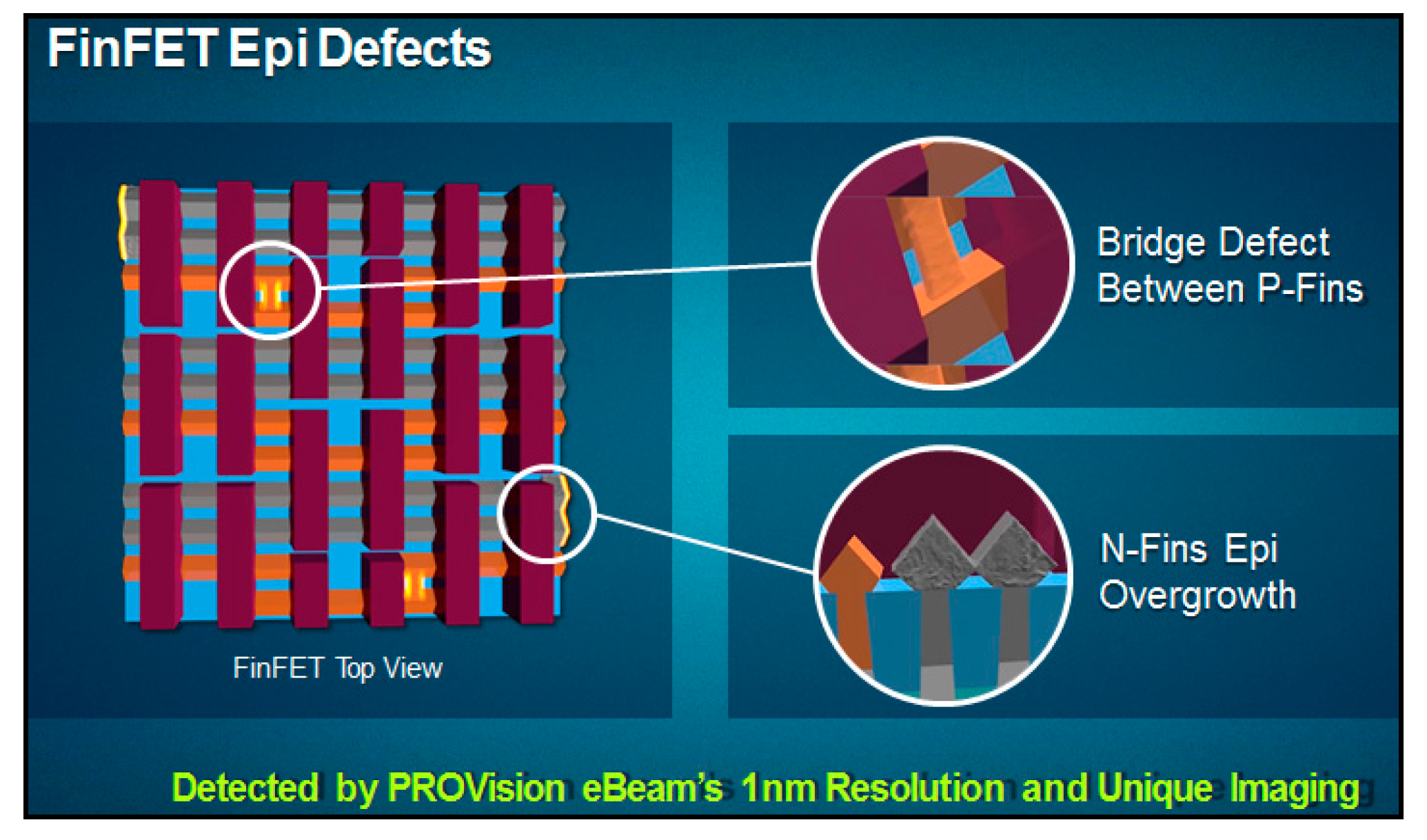
According to Applied Materials [20], as design nodes shrink below 10 nm, defects can get deep-rooted into the FinFET structures. That poses serious new inspection challenges. At such a fine scale, often the defects are buried. It is also hard to see bridge defects that can occur in p-channel field-effect transistor (pFET) structures. (Figure 1). Further, undetected epitaxial overgrowth may happen in n-channel field-effect transistor (nFET). In fact, the process control aspect of it is becoming more important. There are variations. Now that we are controlling things on the atomic level, very small variations can impact the result. It is not just from a defect yield perspective, but also from a device performance perspective [21].
2.1. Patterned Wafer Inspection System
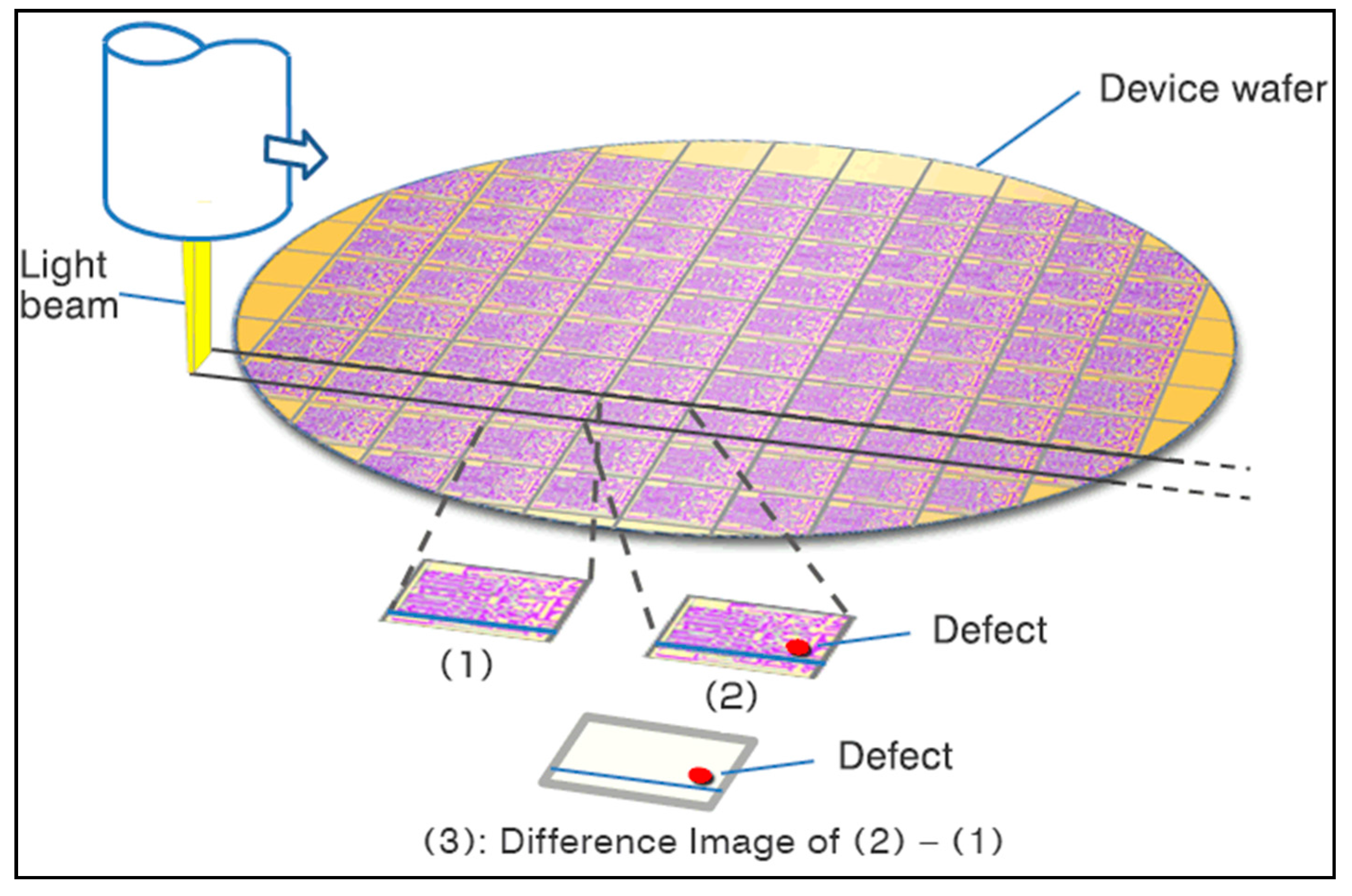
There are many types of patterned wafer inspection systems, including the electron beam inspection systems, the bright-field inspection systems, and the dark-field inspection systems. Each of these has its own features, but the basic detection principles are the same. On a semiconductor wafer, electronic devices of the same pattern are made side by side. Random defects are often caused by particles, such as dust, and occur in random positions, as the name suggests. The possibility that they will occur repeatedly in a position is extremely low. A patterned wafer inspection system can therefore detect defects by comparing the pattern images of adjacent chips (also called dies) and obtaining the difference [22].
Figure 2 shows the principle for detecting defects on a patterned wafer [22]. The pattern on the wafer is captured along the die array by electron beam or light. Defects are detected by comparing image (1) of the die to be inspected with its adjacent die-image (2). If there are no defects, the result of the subtraction of Image (2) from Image (1) by digital processing will be zero and no defects are detected. In contrast, if there is a defect in the image of die (2), the defect will remain in the subtracted image (3), as shown in the figure. The defect is then detected and its position coordinates are registered.
2.2. The Fundamental Use of E-Beam and Optical Inspection
The big market for wafer inspection is the physical defect arena, both e-beam and optical inspections are used to find physical defects in R&D and the foundry. Physical defects, the tiny and/or killer defects in a design, include voids, protrusions, and bridges. The wafer inspection flow involves four parts—engineering analysis; critical line monitoring; line monitoring; and, tool monitoring. e-beam inspection is used for engineering analysis within the R&D groups. Optical inspection is used for line and tool monitoring in the fab. Also, it is used for critical and regular line monitoring to find the defects in wafers. Tool monitoring determines whether a given piece of fab equipment is the root cause of defects on the wafer.
2.2.1. Detecting Defects on a Wafer Using Defect-Specific and Multi-Channel Information
A charged particle beam device for imaging and/or inspecting a sample [23]. The charged particle beam device includes a beam emitter for emitting a primary charged particle beam; and a retarding field device for retarding the primary beam before impinging on the sample, the retarding field device including a magnetic-electrostatic objective lens and a proxy electrode. The charged particle beam device is adapted for guiding the primary beam along an optical axis to the sample for generating secondary particles released from the sample and backscattered particles. The proxy electrode comprises a first opening allowing the passage of the primary beam and at least one second opening for allowing the passage of off-axial backscattered particles. Further, a proxy electrode and a method for imaging and/or inspecting a sample by a charged particle beam are described.
A “charged particle column” [24] is used to direct a beam of finely focused charged particles on any sample surface. Such columns are used in tools to irradiate various types of specimen for the purposes of a variety of applications. The following examples relate to columns built for “electrons” but similarly apply too other “columns” that are used to irradiate charged atoms, also known as “ions”.
Scanning Electron Microscopes (SEMs) are used gather images of specimens at high magnifications. The beam raster’s across a certain area and captures an image. A specific type of SEM, known as a high resolution scanning electron microscope, gathers images at very high resolution and low beam current and is used to measure dimensions of features on the image, whereas a review scanning electron microscope is used to obtain images at specific locations on the surface of semiconductor wafer used for fabricating integrated circuits already identified by another tool as defects/local abnormalities for the purposes of taking high-resolution images of the defects.
2.2.2. E-Beam
Another type of charged particle tool, known as an e-beam defect inspection tool, is used for localizing “defects” that is, local abnormalities on the surface of semiconductor wafer used for fabricating integrated circuits. Another type of charged particle tool, known as an e-beam writer, makes patterns on a photoresist layer that has been coated on a semiconductor wafer or a photolithography mask for the purpose patterning these shapes onto an underlying later. A mask writer operates by illuminating a 1st (square) shaping aperture and forming a 1st shape, then deflecting the 1st shape across a 2nd (square) shaping aperture to form a variable rectangular shape. Since the embodiments described herein are for a defect inspection tool, a further background of conventional defect inspection tools is provided. e-beam defect inspection tools are used in two modes. In a first mode, physical defect inspection, the electron beam gathers images of large enough areas to be able to capture a physical defect or abnormality of interest, that is, the defect physically appears in the area being imaged and is visible in the image created in the detector. Note that the defect need not be “clearly” visible for the inspection tool to operate. It must only generate a signal strong enough to suggest that a defect exists. Once the inspector has localized the defect, it is typically used to gather higher resolution images in a Review SEM, as mentioned above. In a second mode, voltage contrast inspection, changes in potential at the wafer surface are detected. The change in wafer potential may happen because of a “physical defect”, such as a particle or a purely electrical defect such as a dislocation in a crystal causing higher electrical leakage. In either case the e-beam defect inspection tool is sensing the voltage change at location on the semiconductor wafer as the proxy for the defect itself. The voltage change, resulting from the defect typically requires some type of an excitation of the circuit underneath. This can happen as a result of the e-beam, which is being used to sense the voltage contrast itself (also known as passive voltage contrast) or due to an application of a separate electrical bias on the semiconductor wafer (also known as active voltage contrast).
A conventional electron beam inspection, using an electron beam irradiates the target region, thus causing the emission of secondary electrons and a secondary electron detector measures the intensity of the secondary electron emission along the scan path of the electron beam (Figure 3). As a region is scanned, electrons from the electron beam induce surface voltages that vary over the scanned region due to differential charge accumulation of the irradiated features. Voltage contrast inspection operates on the principle that differences in the induced surface voltages over a scanned region will cause differences in secondary electron emission intensities.
As taught, in general, for a given feature, the intensity of secondary electron emission will vary depending on, for example, the landing energy of the beam electrons (primary electrons) and material composition of the feature. For a given material, a secondary electron yield is a measure of a ratio of secondary electron emission to impinging primary electrons as a function of landing energy (eV). Different materials irradiated by an electron beams tuned to a landing energy will emit different intensities of secondary electrons. The different features within the scanned target region will be displayed in an SEM image with different grayscale shades depending on the intensity of secondary electron emission. The irradiated features having a higher intensity of secondary electron emission may be displayed brighter in an SEM image than for those irradiated features having a lower intensity of secondary electron emission.
E-Beam inspection tools (see Figure 3) operate by taking “images” of the semiconductor wafer at high enough resolution. The images are gathered in the areas where the defect must be localized (also known as a “care area”) in one of two ways. Each point of the image is referred to as a pixel.
- Step and scan: The wafer is held stationary to capture an image of the wafer at one location. The process is repeated until the whole care area is covered.
- Swathing: The wafer is moving when the image is being captured so that a whole strip of two-dimensional (2-D) image is created also known as a swath. The process is repeated with multiple swaths until the whole care area has been covered.
One common theme in both of the methods is that the care areas are sampled as full 20 images. The dwell time at each pixel is held constant at each pixel when gathering the image. Once an e-beam inspection tool has gathered an image of the care areas, it must find the defect. This is conventionally done is one of the following ways:
Array mode detection: Here, the image is gathered in an area which has a repeating pattern such as a static random access memory (SRAM) block. With the image, images of the neighboring memory blocks are compared and differences are flagged as a defect.
Random mode detection: Here, images that have been gathered from identical dies of the wafer are compared to each other and differences are flagged as a defect. Note that the dies require a repeating pattern inside as is required for array more inspection.
Die-to data base inspection: Here, the images gathered are compared to a preexisting image saved on the computer and differences are flagged as a defect. The preexisting image may be created artificially from simulation of the inspected areas or from an image of a “golden die” that has been measured prior.
While a conventional e-beam inspection tool produces useful results, they are still less than ideal. An electron beam (E-beam) inspection optimization [25] is provided, in which a plurality of initial inspection regions in a chip are obtained, wherein a center of each of the initial inspection regions is a defect point. Thereafter, reset inspection regions are regenerated without overlap, wherein each of the reset inspection regions is within a scope covered by a field of view (FOV) and the scope contains at least one of the defect points. Afterwards, a center of the reset inspection region is transferred into an inspection center, and then an e-beam inspection is performed on the inspection center.
The inspection flow starts in R&D, where the goal is to capture as many defects as possible. For this, e-beam inspection is used to find the smallest defects, as the technology has sensitivities down to 1 nm. In an e-beam inspection system, the stage moves the wafer to a given location. Then, the electrons hit a small spot size on the wafer. The image data is then collected on a pixel-by-pixel basis. In the electron beam inspection system, electron beam is irradiated onto the surface of the wafer, and the emitted secondary electrons and backscattered electrons are detected. Moreover, the electron beam inspection system detects the amount of the secondary electrons as an image contrast (voltage contrast) according to the conductivity of the device’s internal wiring. If the conductivity at the bottom of the contact hole of the high aspect ratio is detected, the SiO2 residue of ultra-thin thickness can be detected. Traditionally, e-beam inspection has been used for voltage contrast and physical defect applications. In voltage contrast applications, the e-beam inspection tool looks for buried defects (that is, shorts and breaks in structures).
E-beam inspection can find tiny defects that cannot be caught by optical tools. The use of e-beam inspection for the detection of physical defects has become very popular for defect types that have proven difficult for brightfield inspection. However, e-beam inspection throughput is slower than optical. Pre-determining the critical areas of inspection is one way to boost the throughput. e-beam inspection is not used to inspect the entire wafer. Instead, it is used to find defects for only a small part of the wafer. This is called hotspot inspection.
“E-beam still does not have the capability of doing large areas in a timely manner”, said Bob Johnson, an analyst with Gartner. “The real benefit comes from scanning small areas of a die looking for specific defects. While there are some claims that e-beam can scan enough die to get wafer-level defect signatures, these are still done by scanning a very small area on multiple dies on the wafer”. Synopsys design based inspection (DBI) tools provide the accurate small areas of a die looking for defects.
2.2.3. Optical Tools
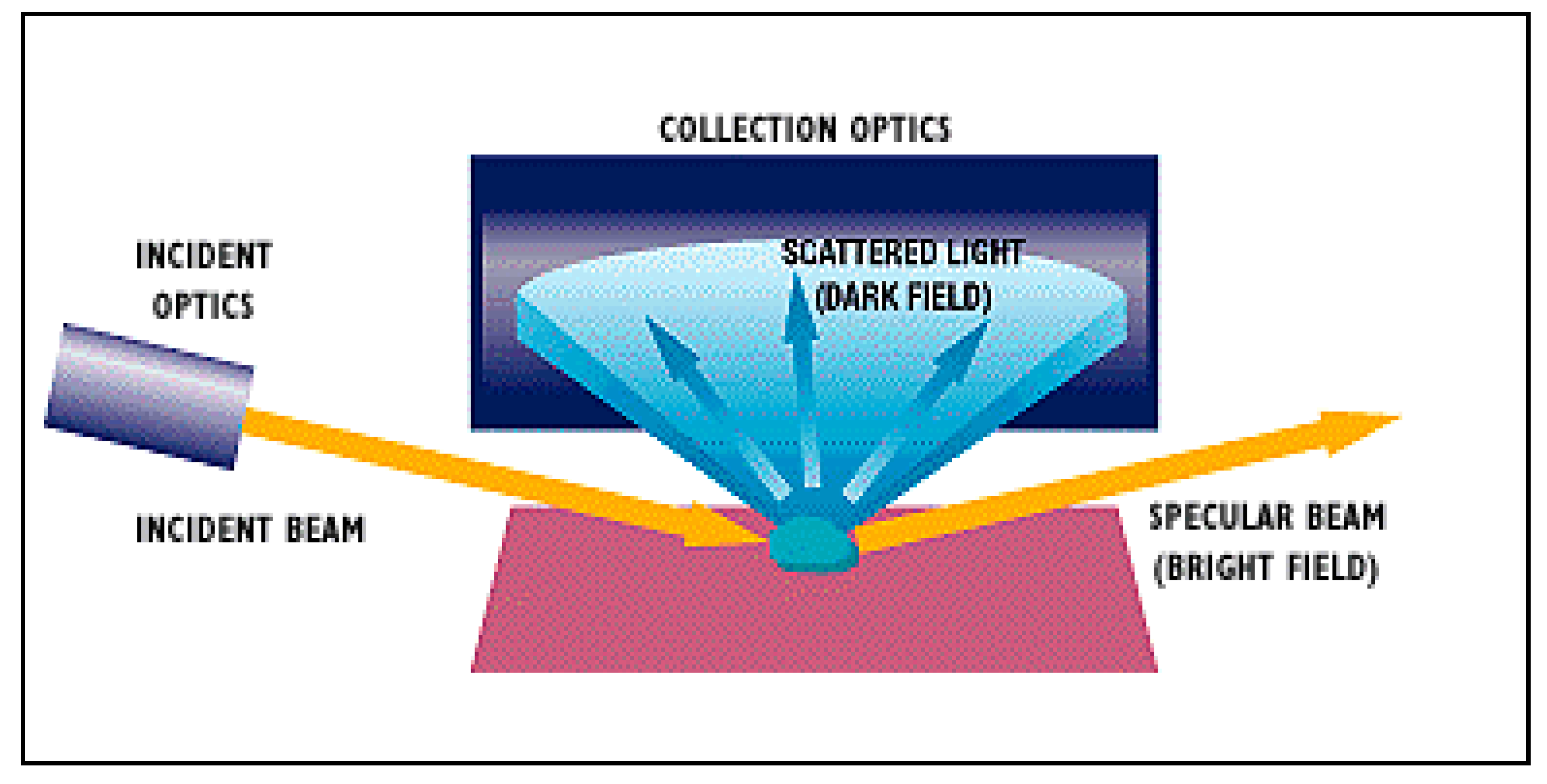
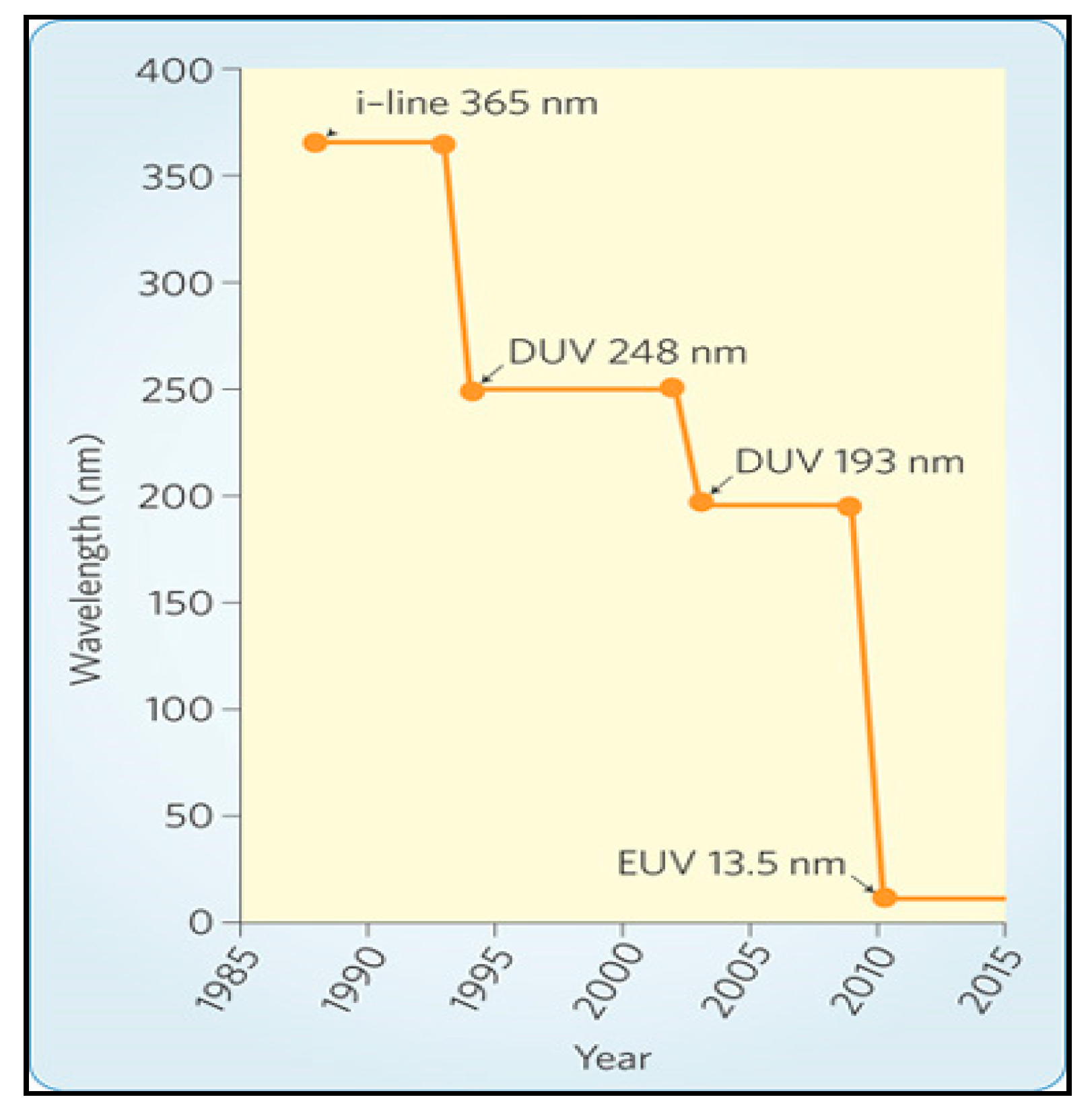
Optical technology in the fab called brightfield inspection (Figure 4), does the job of critical defect finding. Brightfield collects light reflected from a defect. In turn, the defect appears dark against a white background. Chipmakers want an improved signal-to-noise ratio and faster throughputs with optical inspection. Traditionally, the throughputs for critical line monitoring are 1 to 2 wafers an hour. In comparison, optical inspection is used in the production flow. Optical is faster, but it is being stretched to the limit at advanced nodes. Extreme ultraviolet (EUV) wavelength used in wafer inspection is reaching its limits in capturing defects at sub 10 nm design node [26].
Super resolution deep ultraviolet (SR-DUV) wavelength bands, is being discussed as the next capable solution to capture yield-critical defects at 10 nm design nodes and beyond (Figure 5). The SR-DUV is another means to stretch the longevity of Optical inspection tool.
2.3. Techniques Explored to Make E-Beam Inspection Smarter to Compensate for Its Slower Performance
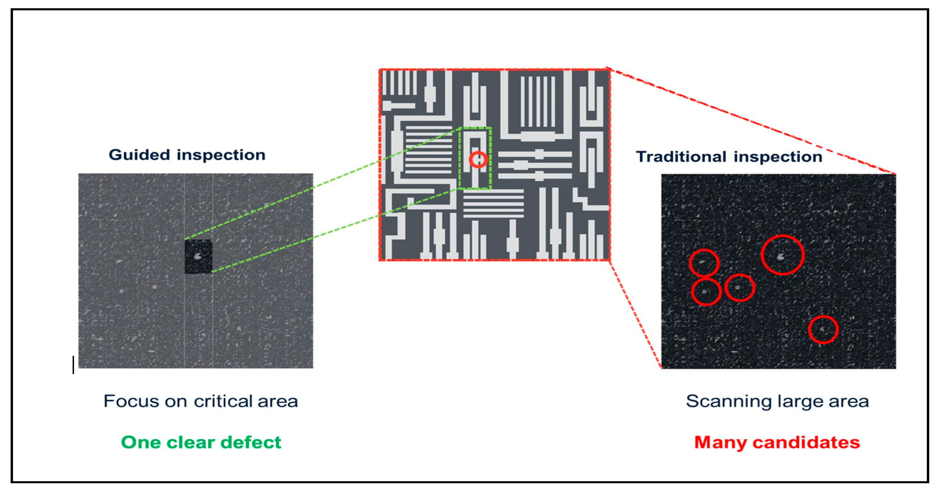
Techniques explored to make e-beam Inspection Smarter include the use of computer aided design (CAD) tools to inspect the targeted critical area and for tools using periodicity for faster turnaround time in recipe creation. Ankush Oberoi at Synopsys Inc. came up with a visionary path breaking solution to the EBI throughput problem statement. He guided the team to work on a targeted ‘Care areas’ using design input. It provided a major path breaking solution to the e-beam Inspection tool throughput issues. Guided inspection on Critical areas, which is provided by Synopsys DBI tool resulted into focused inspection and faster throughput (see Figure 6).
2.3.1. DBI Helps in Faster EBI Recipe Setup
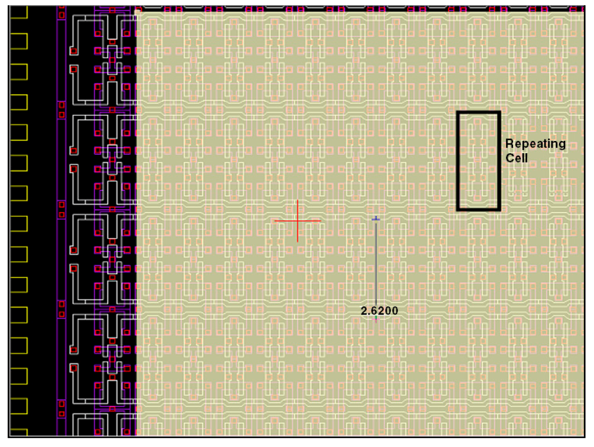
Setting up recipes and finding out areas to inspect and compare directly on the EBI tool is a tedious task if done manually. Calibrating areas using images consumes lot of tool time, there by bringing down productivity of the EBI tool. DBI Recipe Editor helps to expedite this process. It creates Recipe for EBI tool off-line using CAD layout data. This means that no tool time is needed to set up recipe. Also, since the recipe is generated from CAD data, it is more accurate. The ultimate goal of the DBI Recipe Editor is to extract periodically repeating constructs (see Figure 7) in the chip from CAD layout and output bounding rectangles around them (called Die Layout Rectangles) into Recipe in XML format (format defined by PDC). The rectangles are written in Wafer Inspection coordinates (that is, CAD scale, Chip rotation/mirror on Die, CAD offset etc. are applied).
DBI generates recipe which is readily used by EBI. In addition to die layout rectangles, the Recipe XML also contains Design Based Alignment (DBA) targets, which have CAD outline extracted from KDB. EBI tools can use these CAD lines to do fine alignment to enhance the accuracy.
2.3.2. Accuracy Enhancement Using DBI for EBI
DBI helps in narrowing the window of offset for corrections. Figure 8 depicts the spread of critical defects in terms of offset. By applying CAD correction provided by DBI, the offset window is reduced.
2.3.3. Detecting Defects on a Wafer Using Defect-Specific and Multi-Channel Information
Methods and systems for detecting defects on a wafer using defect-specific and multi-channel information is provided [27]. One method includes acquiring information for a target on a wafer. The target includes a Pattern of Interest (POI) formed on the wafer and a known Defect of Interest (DOI), occurring proximate to or in the POI. The method also includes detecting the known DOI in target candidates by identifying potential DOI locations based on images of the target candidates acquired by a first channel of an inspection system and applying one or more detection parameters to images of the potential DOI locations acquired by a second channel of the inspection system. Therefore, the image(s) used for locating potential DOI locations and the image(s) used for detecting defects can be different.
2.3.4. EBI for Complete Wafer Inspection
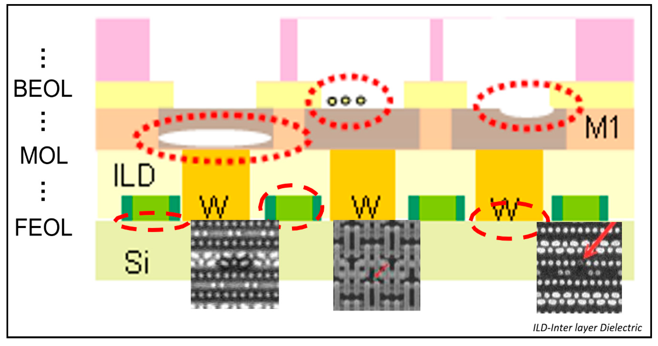
E-Beam Inspection can be used for 100% full wafer inspection [28], which is generally considered a mythical target for EBI. For process layers where the line-widths and defects of interest are large, very large pixel size, and high scan frequency can be used, thereby making full wafer inspection feasible. The metal layers in the back-end-of-line (BEOL) fit this bill when scanned in voltage contrast (VC) mode. Shorts or opens at any previous layer connected to the surface nodes can cause a VC signal, therefore the electrical health of each wafer is assessed for multiple layers simultaneously across the full wafer. The advantage of this scan is that failure sites can be identified and somewhat localized well before wafer final test. This application is more appropriate for semi-mature technologies where there are few defects per wafer, and therefore a full wafer scan is needed to catch a reasonable number of defects. The challenge with this type inspection is in identification of the root cause. A number of studies to map VC defect strength to types of physical defects are described. These studies demonstrated that this technique successfully finds yield limiting defects, but not all yield limiting defects will be detected. A plan for how to use the VC inspection to find root cause is presented below; Electron Beam Inspection has become increasingly important for integrated circuit manufacturing process monitoring and characterization.
Two EBI techniques are in common practice.
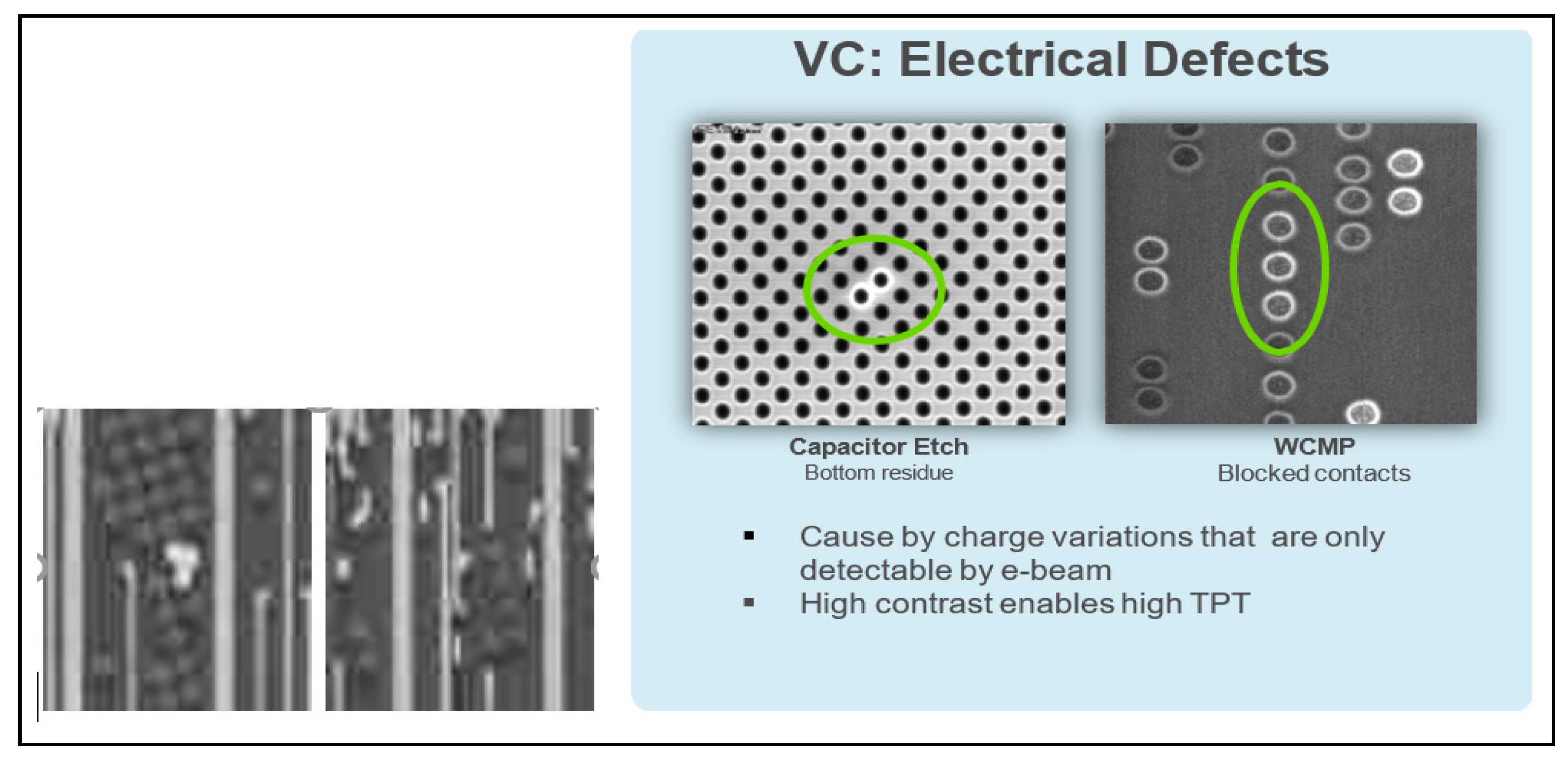
- Voltage contrast inspection: Voltage contrast inspection is used to isolate electrically active defects both buried and at the wafer surface (see Figure 9).
- Physical defect inspection: Physical defect inspection is used to detect defects that may not yet be electrically active but will likely impact yield (see Figure 10).
Both of the approaches suffer from a key limitation, measurement time. Voltage contrast inspections for recent technologies generally use pixel sizes of around 25 nm. At 200 MHz scan rate, this roughly equates to a throughput of 4.5 cm2/h. Physical defect inspections for recent technologies generally use pixel sizes of around 7 nm. At 200 MHz scan rate and 2 scan averages to strengthen the signal, this roughly equates to a throughput of 0.18 cm2/h. Therefore, only a very small fraction of each wafer is generally scanned. A useful category of inspection is large pixel EBI that is competitive with Brightfield Broad-band Plasma (BBP) inspection for throughput. Several 150 nm pixel size, 800 MHz scan rate, 250 nA inspections were created for a recent technology for the purpose of catching BEOL VC defects. For backend layers, the line sizes are large, allowing much larger pixel sizes. The throughput for these inspections is 75 min. per wafer. These inspections detect both bright and dark VC defects, which presumably indicate shorts and opens. Typical results are presented in Section 2. A key challenge with this type of inspection is relating these VC signals to root cause, specifically, identifying the leakage path for shorts and break for opens. While the VC signal alone provides a metric for the health of the wafer, this inspection would be far more useful if root because information could be provided. The first goal is to understand what type of signal different shorts and opens may cause.
Metal 1 Dose Modulated Wafer
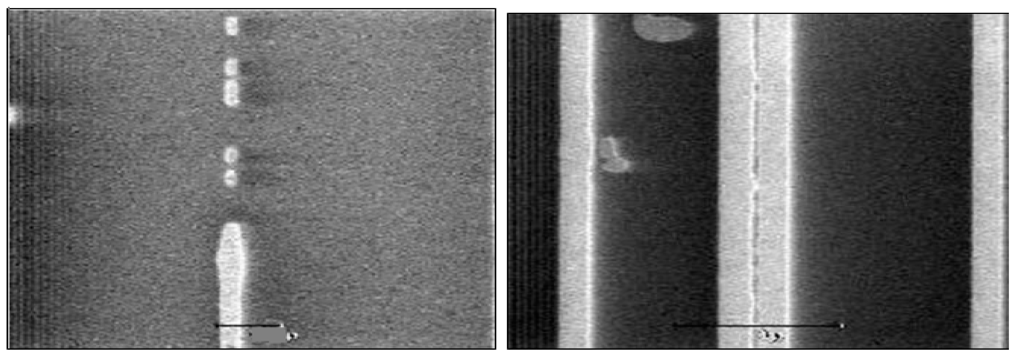
Following are the results of a dose-modulated M1 wafer scan using a large pixel VC inspection (see Figure 11). The modulation is varied by row so that shorts occur in the top rows and opens occur in the bottom rows. Interesting VC defects were reviewed to find the root cause. As the current level was modulated, expectations were high that the root cause could be found in each case. This wafer was also scanned using a physical defect inspection that searches for opens and shorts at known problem locations, a pattern fidelity, and hot spot inspection. Physical defect sites were reviewed in VC mode to see if the physical defects resulted in a VC signal. The results in this section indicate that VC defects picked up with this type of inspection are in fact caused by physical defects. The second half of the results show that not all short and open physical defects will result in a detectible VC signal.
The defects in Figure 11 are not easily detectable. The left portion indicates two large nodes of similar size are shorted together. This short does not significantly change the virtual grounding of either node. Also, the defect highlighted on the right half of the same figure, is not likely to be detectible as well. It is because the open only breaks off a very small line segment, which is less than one 150 nm pixel in size.
Voltage Contrast Signal from Prior Level Physical Defects
Back end of line (BEOL) M5 inspection data for a recent manufacturing technology was reviewed to identify physical defects that might cause electrical failure, both short and open. Figure 12 shows each of the two candidate defects that were identified. These wafers were then scanned with EBI at the next metal level, B1. For the small number of candidate defects that were examined, the short and open defects identified at M5 were not detected at B1. The networks in these process levels are very large. The open on the left of Figure 12 broke a network spanning almost the entire chip into two still very large pieces. The short on the right (in Figure 12), shorted a node spanning almost the entire chip to a second node which contained over 90 um of metal run-length.
Accelerate Time to Review Process
The e-beam technology has a spread of various applications to help accelerate time to review process. The various applications like E-beam inspection followed with SEM review helps in faster and better results. Figure 13 gives a holistic view of the various network of applications, which come into play while using e-beam technology.
Figure 14 depicts the defect detection with device to device (D2D) and chip to chip (C2C) in comparison methodology using e-beam inspection to determine the voltage contrast defect (electrical related) and Physical Defect (Pattern or material related).
Figure 15 depicts Combination of Critical Dimension Unit (CDU) measurement and defect detection. Some physical defects show dependence on the critical dimension (CD) of important structures. Methodology to use these in tandem helps is a value addition to the industry.
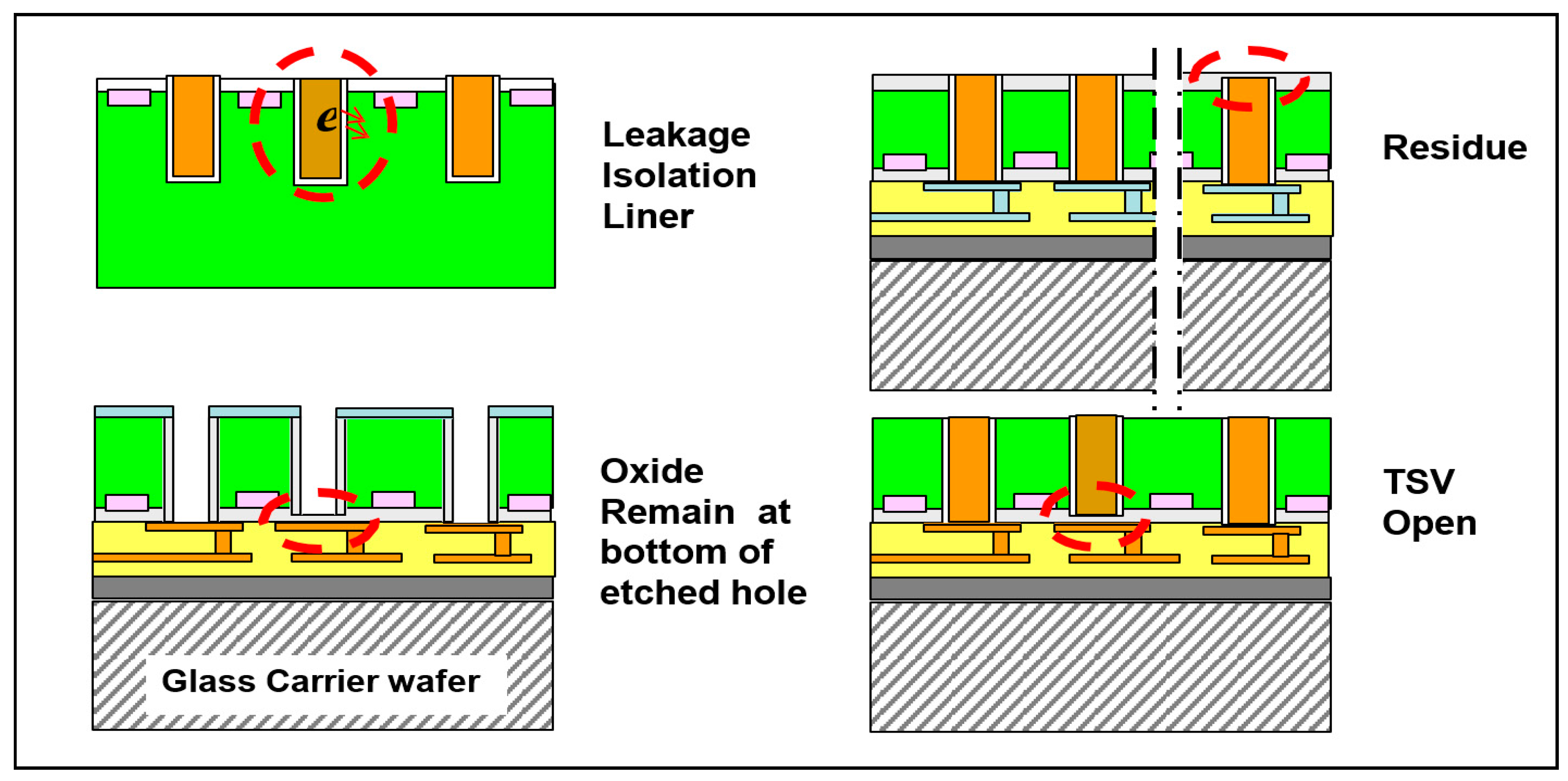
Potential Through-Silicon via (TSV) Application by E-Beam Inspection
There is feasibility study going in to evaluate the e-beam usage in the TSV Open/Leakage detection by Voltage Contrast (VC) and Thin Dielectric Film Remains by Gray Level Comparison [29] (see Figure 16).
Enhanced failure analysis on open TSV interconnects
Through-silicon via (TSV) technology is used for integrated circuit package requirements. 3D stacking of chips results in heat dissipation that provides thermal challenges. To overcome this problem, TSV technology is used for providing both inter-chip and chip-substrate electrical connection having applications in 3-D electronics (see Figure 17 and Figure 18). This allows chips to be interconnected directly providing high speed signal processing resulting in overall improvement of performance by using shortest path for connection. TSV technology is used for 3D integration in place of traditional technologies, such as metal bumps and wire bonding because of reduction in interconnects length, propagation delay, power consumption, and wire parasitic. The use of this technology also helps in providing higher bandwidth. The new potential for EBI would be TSV defect detection. TSV is one of the most critical elements in 3D integration, where defects such as unfilled bottom and holes are very common. Thus, defect detection is of great importance to improve products quality. In this work, a non-destructive TSV defect detection method using Electron beam inspection in compliment to Photo Emission Microscopy (PEM) and Lock-in Thermography (LIT) could play a breakthrough. Some features representative of TSVs are extracted from the images, and then added as an input into a Self-Organizing Map (SOM) network for classification and testing [30]. The results demonstrate that the normal TSVs and defective TSVs can be distinguished obviously by the SOM network. The voids inside the TSVs are further located qualitatively using the Otsu algorithm (Otsu’s algorithm is used to automatically perform clustering-based image thresholding or the reduction of a gray level image to a binary image). The algorithm assumes that the image contains two classes of pixels following bi-modal histogram (foreground pixels and background pixels), it then calculates the optimum threshold separating the two classes so that their combined spread (intra-class variance) is minimal, or equivalently (because the sum of pairwise squared distances is constant), so that their inter-class variance is maximal and verified by the EBI images. These prove the feasibility of EBI of TSV defects with SOM network and Otsu algorithm.
Challenges of open TSV failure analysis include:
Defect localization using Electron Beam Absorbed Current (EBAC) in the EBI where the EBI primary electrons reach the Poly-Si plate at suitable primary energy, and the absorbed current is measured and amplified.
The current divider is active at the (Gate Oxide) GOX short, EBAC current flows partly through the Silicon substrate.
Locally reduced EBAC current at defect site (see Figure 19)
2.4. Understanding on How E-Beam Inspection will Break the Barrier from R&D/Low Volume Production to High Volume Production
Multi-beam Inspection is the key to break the barrier. Currently, Single-column E-beam systems are used in semiconductor foundries for finding defects but are too slow for production. The future lies in multiple-column e-beam technology for high throughput wafer inspection (see Figure 20) [31]. Multi-beam has developed all-electrostatic columns for high-resolution imaging. The elimination of magnetic coils enables the columns to be small; e-beam deflection is faster in the absence of magnetic hysteresis. Multiple miniature columns are assembled in an array. An array of 100 columns covers the entire surface of a 300 mm wafer, affording simultaneous cross-wafer sampling. Column performance simulations and system architecture are presented.
The multi-beam SEM currently uses multiple electron beams in a single column and one dedicated detector for each beam to alleviate Coulomb interaction limitations and bypass the detector bandwidth limit [32]. The principle of operation is depicted in Figure 21. A multiple beam electron source produces a regular array of electron beams that are imaged onto the sample, forming a pattern of multiple primary electron foci. The array of primary beams is arranged in a hexagonal pattern to minimize electron optical aberrations. The SEMs that emanate from each primary electron spot are imaged onto a multi-detector with one detection unit for each electron beam. A magnetic sector field separates primary electron and SEM beams. The electron beams are scanned over the sample, and the SE signal is recorded for each scan position as in conventional SEMs. One single scanning pass thus produces multiple images in parallel yielding a complete image of the sample region underneath the primary beam array. A number of options for producing an array of electron beams has been demonstrated.
2.5. Study of Leading Commercial Optical and E-Beam Products
Various companies have adapted e-beam technology for inspection.
- KLA-Tencor eS805TM Electron-Beam Inspection System launch in 2013. However, no known new development has been published on this.
- HERMES–MicroVision Inc. (HMI, Hsinchu, Taiwan) eScan® 320xp and eScan® 500 E-beam inspection system.
- eScan® is capable of generating defectivity baseline for both physical and electrical defects. eScan®’s main applications include: front-end of line at Salicide, high-k metal gate (HKMG) and FinFET; mid-end of line at contacts, and back-end of line at via and copper chemical mechanical polishing (CMP) [33].
- Applied Materials ProVision Tool.The Applied PROVisionTM system (see Figure 22) is the industry’s most advanced e-beam inspection tool, incorporating innovations based on more than 20 years of leading expertise in e-beam technology for review and metrology [34]. It is the only e-beam hotspot inspection tool offering down to 1 nm resolution, allowing customers to detect the most challenging “killer” defects that other technologies cannot find, and to monitor process marginality to rapidly resolve ramp issues and achieve higher yields. Provision allows capturing defects they could not see before (Figure 23). The system can detect, for example, epi-overgrowth in FinFETs. “While the epi overgrowth is clearly visible on the PROVision, it’s almost impossible to see in conventional EBI. Without the resolution and the special imaging, it is very difficult to catch that.
- KLA Tencor
Number of pixels inspected increases by 2 times per node to maintain required sensitivity.
Ebeam Spot size limited by Coulomb interactions. Ebeam Spot ~ √ (Beam Current). Optical Spot is independent of light level.
Each node drives √2 smaller spot, which in turn drives 2 times lower Beam Current for specific system.
Therefore, Data Rate decreases by 2 times per node to maintain constant noise.
EB Systems slow down 4 times per node.
Best to date: Inspect 32 nm mask <20 h.
100 × 100 mm2 area 10% Δ CD.
2.6. Roadmap of Semiconductor Inspection Technology Down to 1 nm
There are technical challenges facing the semiconductor industry as Moore’s law moves from its fifth to sixth decade [36]. The technology roadmap to advance computing looks strong for the rest of this decade from a technical perspective, as seen in Figure 27 and Figure 28. Therefore, the continuing revolution in computing technology towards ever increasing levels of capability and mobility is within reach. The key challenges faced in driving Moore’s Law into the sub-10 nm regime are, first, semiconductor manufacturing is increasing exponentially in complexity. This complexity has multiple facets. The sheer number of transistors in a leading-edge integrated circuit now numbers in the billions. Managing design, debug, development, product introduction, yield, and manufacturing requires continued advances in the capability of the entire semiconductor ecosystem. The number of different films, materials, and critical interfaces in the process flow is increasing dramatically Second, cost is becoming a dominant concern in semiconductor manufacturing. The cost of manufacturing, whether measured by capital expenditure to achieve a given capacity level or measured by the cost to manufacture an integrated circuit die, is rapidly increasing. In the past, increased capital intensity resulted in reduced die-level manufacturing cost. Going forward, this gain is at risk. Furthermore, the cost of research and development to create leading-edge manufacturing processes is increasing due to the cost of capital for development equipment sets and the cost of complexity with so many human and technical interfaces needing to be carefully managed to deliver new manufacturing technologies at the two-year cadence of Moore’s Law.
Finally, the cost of manufacturing and development is leading to significant concentration in the semiconductor manufacturing base. The top three semiconductor manufacturers now routinely account for more than 60% of capital investment on an annual basis. This concentrated buying power of products and services is driving the associated trend of consolidation in the supplier base, particularly for semiconductor capital equipment suppliers. This concentration of activity is leading to a reduction in the diversity of competing technology solutions. As such, new business models and collaboration models are developing to align and tightly integrate development roadmaps between manufacturers and equipment suppliers. With such high research and development costs, there is little or no margin for delay or failure.
2.7. Evolution of Less than 1 nm Node Inspection System
2.7.1. Current State of Technology
Small spot resulting from lower density of electrons. The ability to find defects in complex FinFET structures. Difficulty in detection of defects in process margins.
2.7.2. Challenges Faced
Maintaining both low throughput along with higher resolution. Monitoring of epi growth along with defects found in deep trenches of the structure. Problems related to detection of defects in case of multi-patterning and 3D structures during the process control.
2.7.3. Upcoming Technologies
Higher density of electrons with small spot size resulting in better resolution along with higher throughput. Higher resolution systems providing clear view of the bridge defects being found in advanced nodes specifically with size of less than 1 nm. Massive sampling of different measurements of 3D structures for understanding the defects by process characterization and process control.
2.7.4. Key Points
Advanced e-beam Systems with less than 1 nm Design Node Inspection: With all of the above complexities being taken care of in advanced e-beam node inspection system, this has extensive usage in R&D sector allowing high detection in nuisance environment, reducing the ramp time and overall optimization of yield across volume production.
With advancements being made in the e-beam inspection system, the next 5 to 10 years may result in growth of advanced nodes posing challenges towards the detection of defects in these advanced nodes through changes in e-beam.
3. Discussion
Optical technology been accompanying the IC era to date. There is no doubt that it is a very well established and conventional art in the wafer inspection trade. The IC industry is reorienting its geometry and packing density to meet the ever growing demands of changing times. Due to its inherent physical limitations, the optical method simply cannot see the measuring rod of silicon industry which is getting re-calibrated to finer nano-scales. Defects that are deep inside the complex silicon, cannot be noticed by optical instruments. Naturally, for 10 nm and even below, a high resolution is needed, which EBI can readily yield. However, EBI on its own suffers inherent drawbacks of poor productivity. Yet however, when it is used wisely, as demonstrated in this articulation, in the smart E-beam way, it does yield positive results. With adoption of EBI, industry has been able to unearth, the deeply hidden defects of the silicon-real estate, which otherwise gets through the production line, scot-free. EBI can be used for 100% full wafer inspection. The encouraging results of this research show as to how using improvised techniques and optimal processes in conjunction with EBI, in effect, unleashes the real potential of this technology. The actual merits and powerful resolution capabilities of EBI, do far outweigh its short-falls, as long as it is used with a well-crafted, engineered, and optimized manner with the smart E-beam school of thought.
4. Conclusions
With shrinking geometries, it is becoming difficult to use Optical inspections to detect systematic defects. EBI is the answer to the industry’s requirement due to its astonishing 1 nm resolution. With improved techniques to enhance the throughput, EBI is well placed to take on the role of Wafer Inspection work horse. Additionally, it is clear that, the need of overall inspection will grow at lower nodes, thus propelling the growth of this segment. It is also expressed here, that this research and experimentation did offer considerable learning experience, thus paving the way to improve and align commercial product offering to better serve the Semiconductor Industry.
Acknowledgments
The author/s would like to take this opportunity to gratefully acknowledge the commitment of Synopsys board of directors towards supporting its R&D potential to strengthen the Organization’s position in the new horizons of semiconductor solutions trade. Our customers’ suggestions and their industry needs have been an influential ingredient to align our R&D focus and efforts towards contemporary issues that are relevant to the technology and the market-place. Appreciations to all our engineering, marketing, R&D, product development group, quality assurance (QA), computer-aided engineering (CAE) for their precious contributions, and to all those who have directly or indirectly supported the success of this research & product solution offering.
Author Contributions
Ankush Oberai organizes the materials and writes the manuscript. Jiann-Shiun Yuan provides the technical feedback. Both authors proofread the manuscript. Ankush Oberai is a senior director at Synopsys where he is supervising the failure analysis team.
Conflicts of Interest
The authors declare no conflict of interest.
Abbreviations and Acronyms
| ACI | After Clean Inspection |
| BBP | Brightfield Broad-band Plasma |
| BEOL | Back End of Line |
| C2C | Cell to Cell |
| CAD | Computer Aided Design |
| CD | Critical Dimension |
| CD SEM | Critical Dimension Scanning Electron Microscopes |
| Cu-CMP | Copper Chemical Mechanical Polishing |
| D2D | Die to Die |
| DBA | Design Based Alignment |
| DBI | Design Based Inspection |
| DOI | Defect of Interest |
| DRAM | Dynamic Random Access Memory |
| EBAC | Electron Beam Absorbed Current |
| EBI | Electron Beam Inspection |
| FOV | Field of View |
| GOX | Gate Oxide |
| HKMG | High-k (k-dielectric) Metal Gate |
| IC | Integrated Chip |
| LIT | Lock-in Thermography |
| PDC | Process Diagnostic Control |
| PEM | Photo Emission Microscopy |
| POI | Pattern of Interest |
| SEM | Scanning Electron Microscopes |
| SOM | Self-Organizing Map |
| SR-DUV | Super Resolution Deep Ultraviolet |
| SE | Secondary electrons |
| TSV | Through-Silicon Via |
| VC | Voltage Contrast |
| WCMP | Tungsten Chemical Mechanical Polishing |
References
- Raplee, J.; Plothowski, A.; Kirka, M.; Dinwiddie, R.; Okello, A.; Dehoff, R.; Rabu, S. Themographic microstructure monitoring in electron beam additive manufacturing. Sci. Rep. 2017, 7, 43554. [Google Scholar] [CrossRef] [PubMed]
- Childres, I.; Foxe, M.; Jovanovic, I.; Chen, Y. Effect of energetic electron irradiation on graphene and graphene field-effect transistors. Proc. SPIE 2011, 8031, 803122-1–803122-8. [Google Scholar] [CrossRef]
- Van Himbergen, H.; Nijikerk, M.; de Jager, P. High throughput defect detection with multiple parallel electron beams. J. Vac. Sci. Technol. B 2007, 25, 2521. [Google Scholar] [CrossRef]
- Cai, N.; Zeng, X.; Wu, K.; Song, H.; Gao, W.; Tian, Q.; Lei, C.; Gao, K.; Wang, L.; Zhao, Y. Automated Klarf-Based Defect Inspection by Electron-Beam Inspection Tool: A Novel Approach to Inline Monitoring and/or Process Change Validation. Proc. SPIE 2016, 9778. [Google Scholar] [CrossRef]
- Propabality of Defect Detection of Posiva’s Electron Beam Weld. Available online: http://www.posiva.fi/files/3527/WR_2013-70.pdf (accessed on 20 September 2017).
- Patterson, O.; Lee, J.; Let, C.; Salvado, D. E-beam inspection for detection of sub-design rule physical defects. In Proceedings of the Annual SEMI Advanced Semiconductor Manufacturing Conference, Saratoga Springs, NY, USA, 15–17 May 2012. [Google Scholar] [CrossRef]
- Lin, P.; Cai, N.; Eah, S.; Patteron, O.; Gao, W. E-beam mechanics and net connectivity for interlayer short detection: DI: Defect inspection and reduction. In Proceedings of the Annual SEMI Advanced Semiconductor Manufacturing Conference, Saratoga Springs, NY, USA, 15–18 May 2017; pp. 256–261. [Google Scholar]
- Hafer, R.; Patterson, O.; Hakn, R.; Xiao, H. Full-wafer voltage contrast inspection for detection of BEOL defects. In Proceedings of the Annual SEMI Advanced Semiconductor Manufacturing Conference, Saratoga Springs, NY, USA, 15–17 May 2017; pp. 461–468. [Google Scholar]
- Liao, H.; Luoh, T.; Yang, L.; Yang, T.; Chen, K.; Lu, C.; Lin, D.; Lv, R.; Hsiang, C.; Hu, C. Tiny physical defects inspection by optimized EBI methodology. In Proceedings of the e-Manufacturing & Design Collaboration Symposium, Hsinchu, Taiwan, 12 September 2014; pp. 1–3. [Google Scholar]
- Zhou, X.; Guo, Y.; Jones, J. E-beam inspection BVC (Bright Voltage Contrast) verification for 14 nm technology: DI: Defect inspection and reduction. In Proceedings of the Annual SEMI Advanced Semiconductor Manufacturing Conference, Saratoga Springs, NY, USA, 15–18 May 2017; pp. 234–239. [Google Scholar]
- Speeding up E-Beam Inspection. Available online: http://semiengineering.com/speeding-up-e-beam-inspection/ (accessed on 20 August 2017).
- Cooray, A. Extragalactic background light measurements and applications. R. Soc. Open Sci. 2016, 3, 150555. [Google Scholar] [CrossRef] [PubMed]
- Prescop, T.; Tran, C.; Monahan, K.; Lam, D.; Liu, E. Multiple column high-throughput e-beam inspection (EBI). Proc. SPIE 2012, 8324. [Google Scholar] [CrossRef]
- Kaestner, M.; Hofer, M.; Rangelow, I. Mix & match electron beam & scanning probe lithography for high throughput sub-10 nm lithography. Proc. SPIE 2013, 8680. [Google Scholar] [CrossRef]
- Bunday, B.; Mukhtar, M.; Quoi, K.; Thiel, B.; Malloy, M. Simulating massively parallel electron beam inspection for sub-20 nm defects. Proc. SPIE 2015, 9424. [Google Scholar] [CrossRef]
- Xiao, H.; Ma, L.; Wang, F.; Zhao, Y.; Jau, J.; Selinidis, K.; Thompson, E.; Sreenivasan, S.; Resnick, D. Inspection of 32 nm imprinted patterns with an advanced E-Beam inspection system. Proc. SPIE 2009, 7488. [Google Scholar] [CrossRef]
- Hayashi, H.; Fukunaga, Y.; Yamasaki, M.; Nagai, T.; Yamazaki, Y. Development of voltage contrast defect inspection technique for line monitoring 300 mm ULSI hp90 logic contact layer. Proc. SPIE 2005, 5752, 997–1008. [Google Scholar]
- Adler, D.; McCord, M.; Vaez-Iravani, M.; Han, L.; Bertsche, K. High-Speed Electron Beam Inspection. U.S. Patent US7315022 B1, 6 January 2008. [Google Scholar]
- Kemen, T.; Malloy, M.; Thiel, B.; Mikula, W.; Denk, W.; Dellemann, G.; Zeidler, D. Further advancing the throughput of a multi-beam SEM. Proc. SPIE 2015, 9424. [Google Scholar] [CrossRef]
- Applied Materials intros High res E-Beam Inspection System. Available online: http://semimd.com/blog/2016/07/11/applied-materials-intros-high-res-e-beam-inspection-system/ (accessed on 22 August 2017).
- E-Beam vs. Optical Inspection. Available online: https://semiengineering.com/e-beam-vs-optical-inspection/ (accessed on 26 August 2017).
- Wafer Defect Inspection System. Available online: http://www.hitachi-hightech.com/global/products/device/semiconductor/inspection.html (accessed on 10 September 2017).
- Frosien, J. Charged Particle Beam Device and Method for Inspecting and/or Imaging a Sample. U.S. Patent 9601303, 21 March 2017. [Google Scholar]
- Mankos, D.; Hess, C.; Ciplickas, D. E-beam Inspection Apparatus and Method of Using the same on Various Integrated Circuit Chips. U.S. Patent 9496119, 15 November 2016. [Google Scholar]
- Luoh, T.; Yang, L.; Yang, H.; Chen, K. Electron Beam Inspection Optimization. U.S. Patent 9116108, 25 August 2015. [Google Scholar]
- Why EUV Is so Difficult. Available online: https://semiengineering.com/why-euv-is-so-difficult/ (accessed on 9 August 2017).
- Wu, K.; Gao, L.; Chen, H.; Shortt, D. Detecting Defects on a Wafer Using Defect-Specific and Multi-Channel Information. U.S. Patent 9552636, 24 January 2017. [Google Scholar]
- Hafer, R.; Patterson, O.; Hahn, R.; Xiao, H. Full-wafer electron beam inspection for detection of BEOL defects. In Proceedings of the 25th SEMI Advanced Semiconductor Manufacturing Conference (ASMC), Saratoga Springs, NY, USA, 19–21 May 2014. [Google Scholar]
- Beyersdorfer, J.; Altman, F.; Schrank, F. Enhanced Failure Analysis on Open TSV Interconnects. In Proceedings of the International Symposium for Testing and Failure Analysis American Society for Metals, Phoenix, AZ, USA, 11–15 November 2012. [Google Scholar]
- Shen, J.; Chen, P.; Su, L.; Shi, T.; Tang, Z.; Liao, G. X-ray inspection of TSV defects with self-organizing map network and Otsu algorithm. Microelectron. Reliab. 2016, 67, 129–134. [Google Scholar] [CrossRef]
- Holcman, I. Joint assessment of novel multi column E-beam inspection system. In In Proceedings of the 2013 EMICON Europa Workshop on Equipment Assessment & Equipment Performance Improvements, Berlin, Germany, 8–10 October 2013. [Google Scholar]
- Eberle, A.; Mikula, S.; Schalek, R.; Lichtman, J.; Knothe, M.; Zeidler, D. High-resolution, high-throughput imaging with a multibeam scanning electron microscope. J. Microsc. 2015, 259, 114–120. [Google Scholar] [CrossRef] [PubMed]
- Hermes Microvision eScan Series. Available online: http://www.hermes-microvision.com/Products/ (accessed on 1 September 2017).
- Applied Materials’ Next-Generation E-Beam Inspection System Provides Industry’s Highest Resolution. Available online: http://www.appliedmaterials.com/company/news/press-releases/2016/07/applied-materials’-next-generation-e-beam-inspection-system-provides-industry’s-highest-resolution (accessed on 15 August 2017).
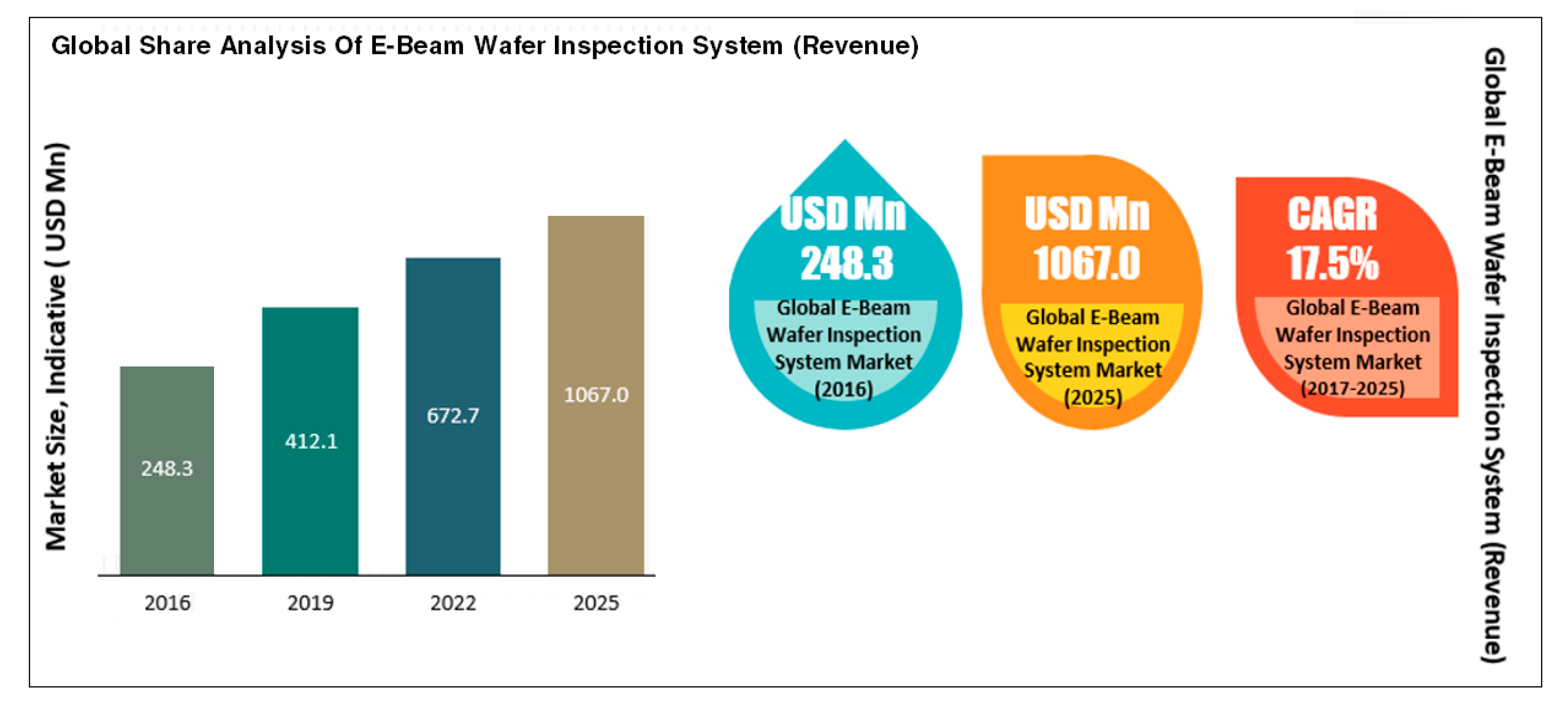
- Global E-Beam Wafer Inspection System Market 2017–2021. Available online: https://www.researchandmarkets.com/reports/4027530/global-e-beam-wafer-inspection-system-market-2017 (accessed on 24 August 2017).
- Schuegraf, K.; Abraham, M.; Brand, A.; Naik, M.; Thakur, R. Semiconductor logic technology innovation to achieve sub-10 nm manufacturing. IEEE J. Electron Devices Soc. 2013, 1, 66–75. [Google Scholar] [CrossRef]
Figure 1.
Bridge defect and Epi overgrowth detected by e-beam image. Challenges faced for Fin field-effect transistor Electron Beam Inspection (EPI) undetected defects can be detected by e-beam inspection.
Figure 1.
Bridge defect and Epi overgrowth detected by e-beam image. Challenges faced for Fin field-effect transistor Electron Beam Inspection (EPI) undetected defects can be detected by e-beam inspection.

Figure 2.
Principles of defect detection on a patterned wafer; a die-to-die image comparison principle is used to detect the defects.
Figure 2.
Principles of defect detection on a patterned wafer; a die-to-die image comparison principle is used to detect the defects.

Figure 3.
Schematic of e-beam generation projection to a wafer where the principle of e-beam inspection tool is depicted.
Figure 3.
Schematic of e-beam generation projection to a wafer where the principle of e-beam inspection tool is depicted.
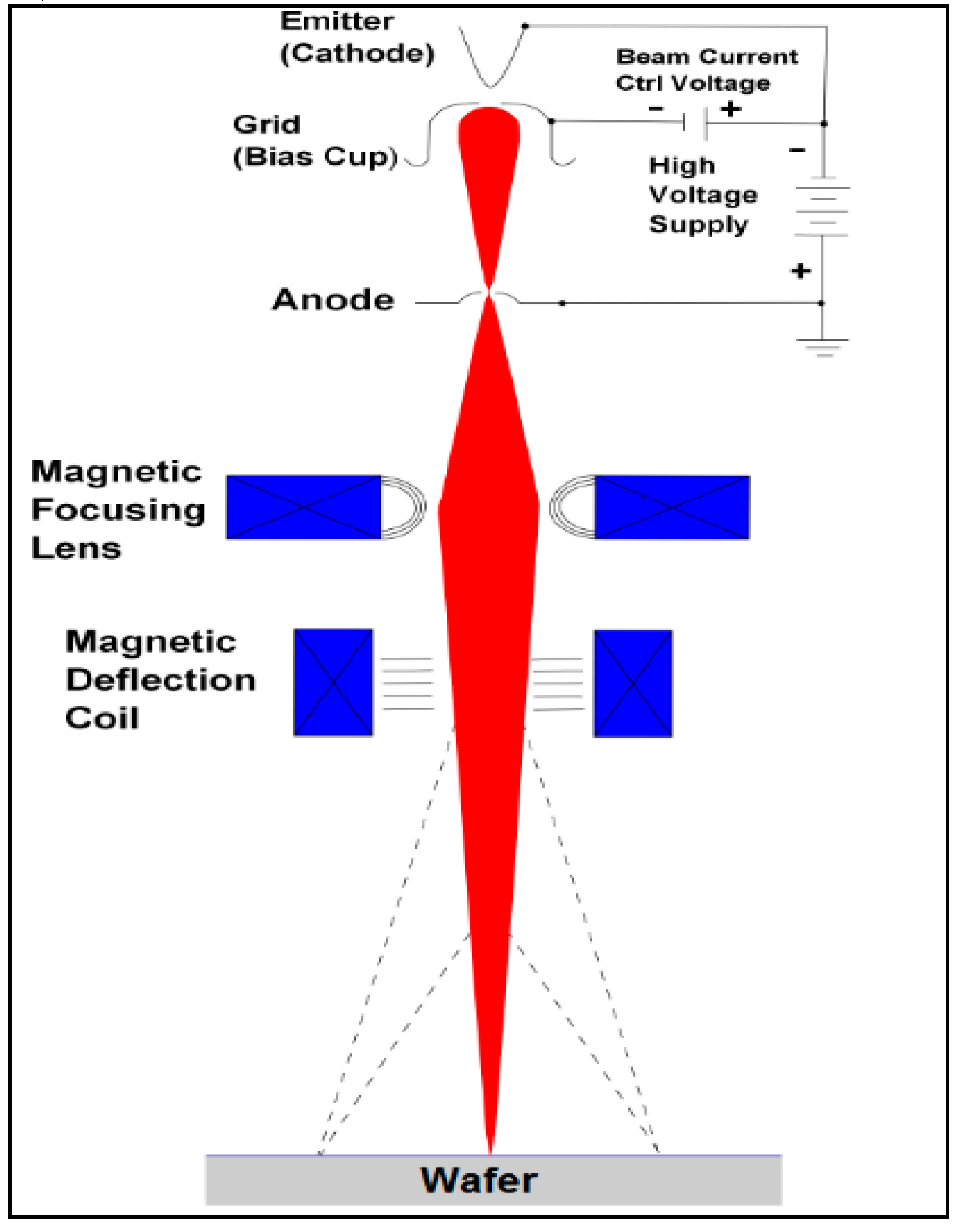
Figure 4.
Basic principle of light scattering used in optical inspection. Incident beam from the left yields the specular beam (bright field) to the right.
Figure 4.
Basic principle of light scattering used in optical inspection. Incident beam from the left yields the specular beam (bright field) to the right.

Figure 5.
Evolution of light wavelengths used for optical inspection. The latest being super resolution deep ultraviolet (SR-DUV).
Figure 5.
Evolution of light wavelengths used for optical inspection. The latest being super resolution deep ultraviolet (SR-DUV).

Figure 6.
Comparison between guided and traditional inspections. A guided inspection produces a clear defect, while the traditional inspection results in many defect candidates.
Figure 6.
Comparison between guided and traditional inspections. A guided inspection produces a clear defect, while the traditional inspection results in many defect candidates.

Figure 7.
Overlay of die layout rectangle over layout polygons of repeating structures. The repetitive structures are marked separately as pattern of interest and specific inspection parameters are applied during inspection.
Figure 7.
Overlay of die layout rectangle over layout polygons of repeating structures. The repetitive structures are marked separately as pattern of interest and specific inspection parameters are applied during inspection.

Figure 8.
Spread of critical defects and corrections made using the computer aided design tool and optical technologies.
Figure 8.
Spread of critical defects and corrections made using the computer aided design tool and optical technologies.
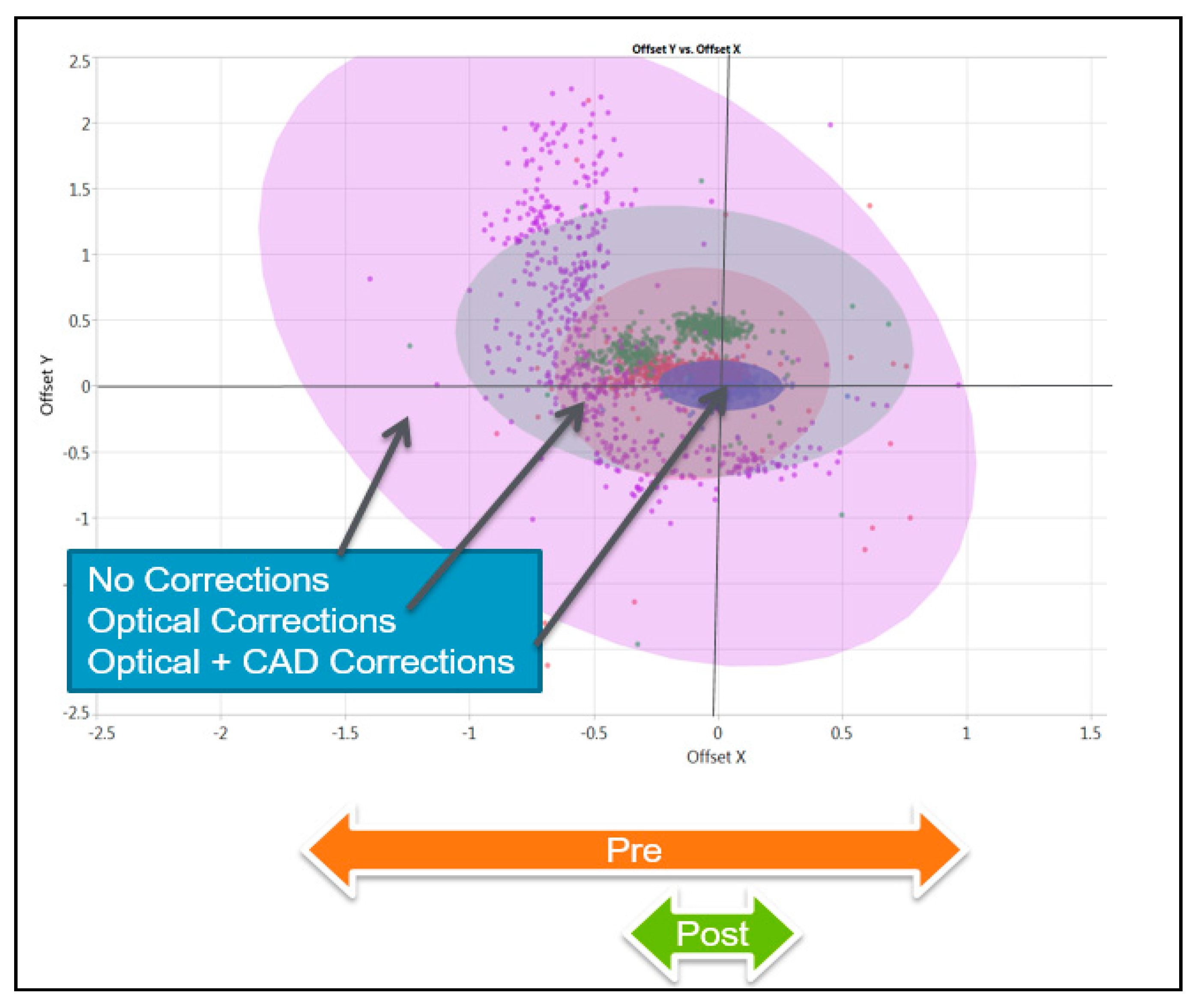
Figure 9.
Voltage contrast electrical defects caused by charged variations are detectable by e-beam.
Figure 9.
Voltage contrast electrical defects caused by charged variations are detectable by e-beam.

Figure 10.
Physical defects detected by edge contrast signal using E-beam.
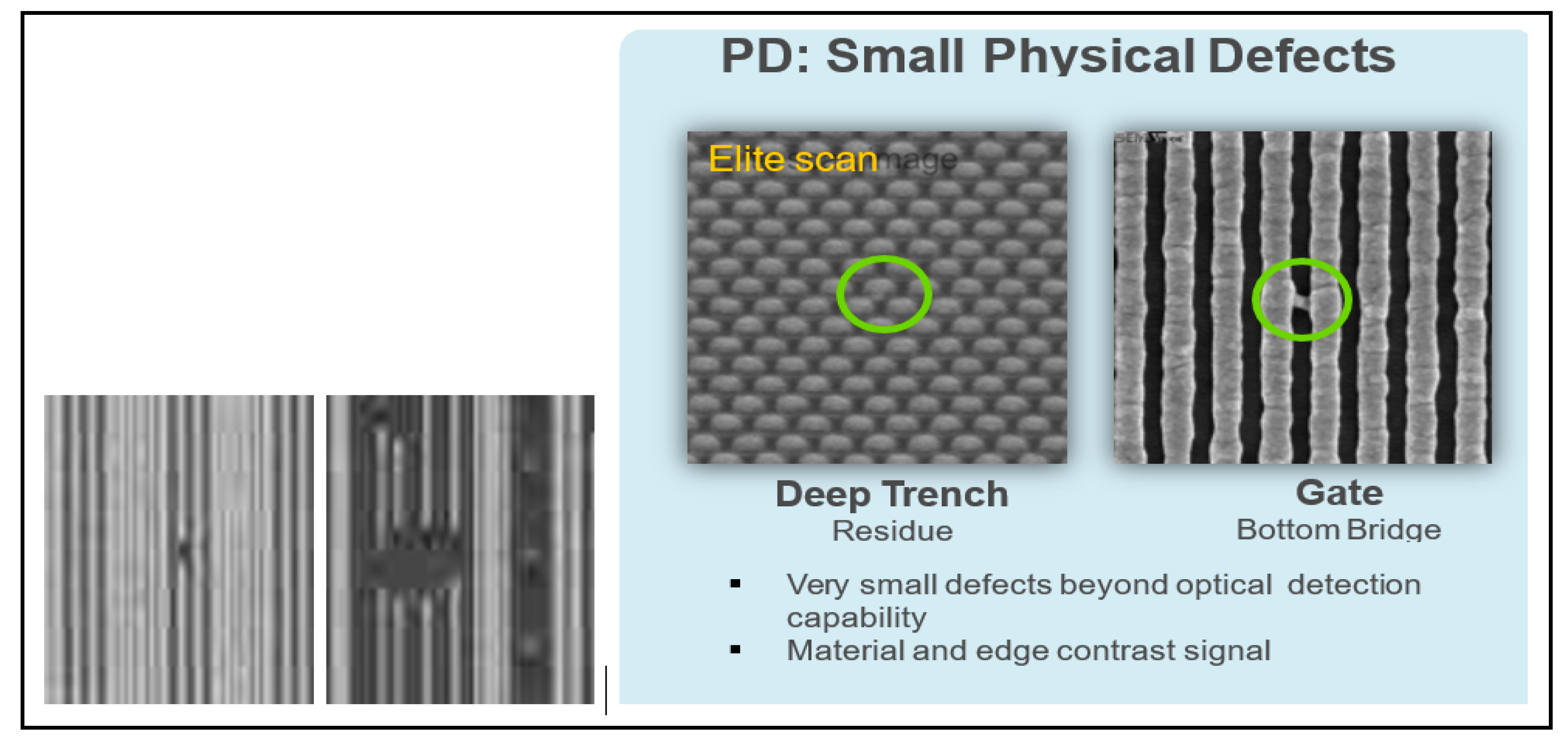
Figure 11.
Dose modulated wafer inspection using e-beam to correlate physical defects with voltage contrast signal variations.
Figure 11.
Dose modulated wafer inspection using e-beam to correlate physical defects with voltage contrast signal variations.
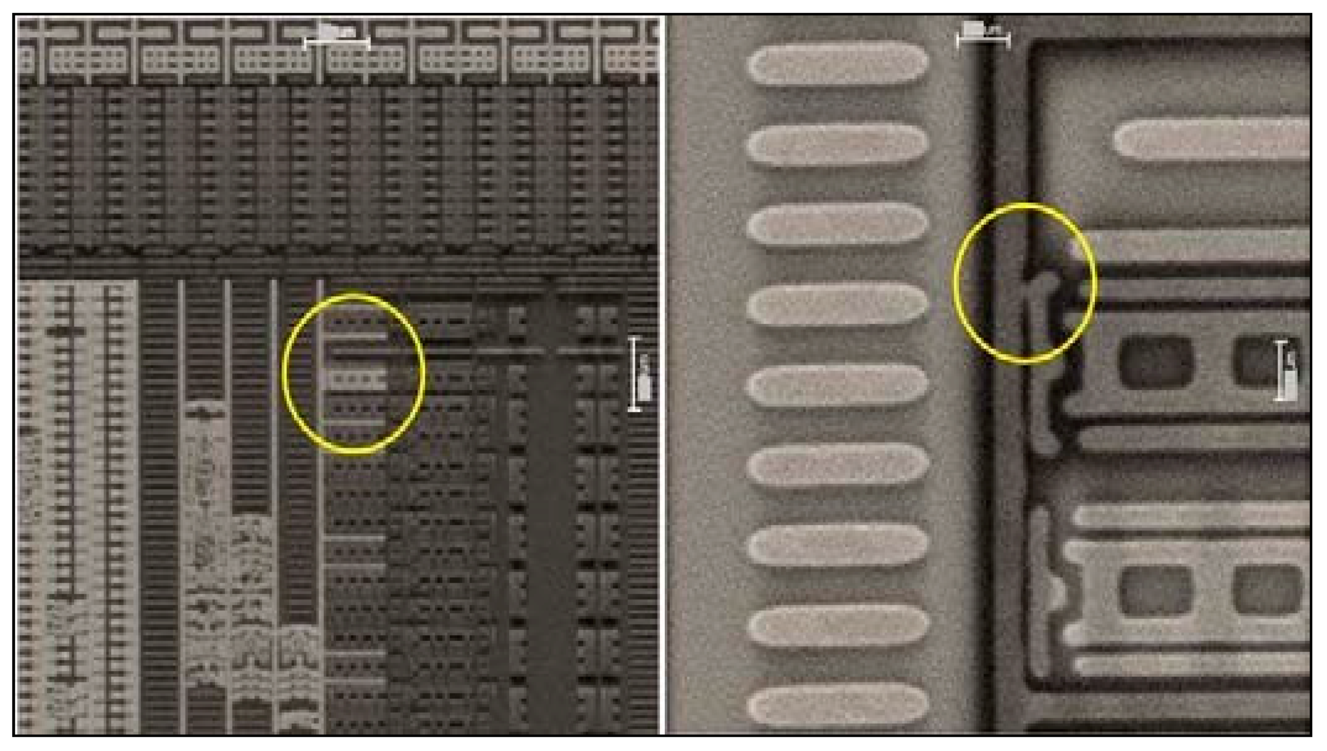
Figure 12.
Two candidate defects which were shorts that spanned almost the entire chip.

Figure 13.
E-Beam technology and its allied areas.

Figure 14.
Defect detection with die to die/chip to chip.

Figure 15.
Combination of critical dimension unit Measurement and defect detection giving an overall value addition.
Figure 15.
Combination of critical dimension unit Measurement and defect detection giving an overall value addition.
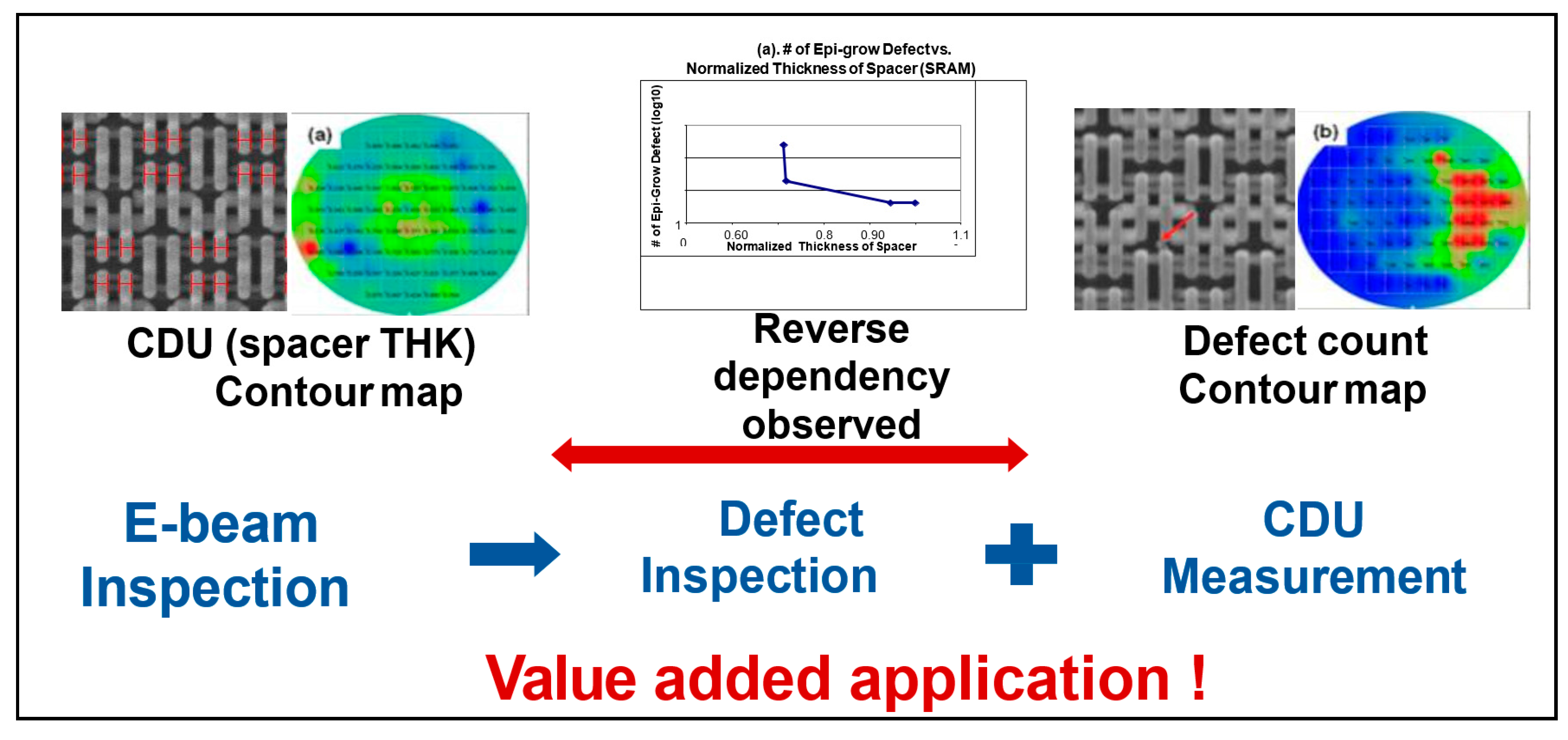
Figure 16.
Sample TSV open defect due to left over oxide at bottom of etched hole.

Figure 17.
TSV inter-chip and chip-substrate electrical connection.
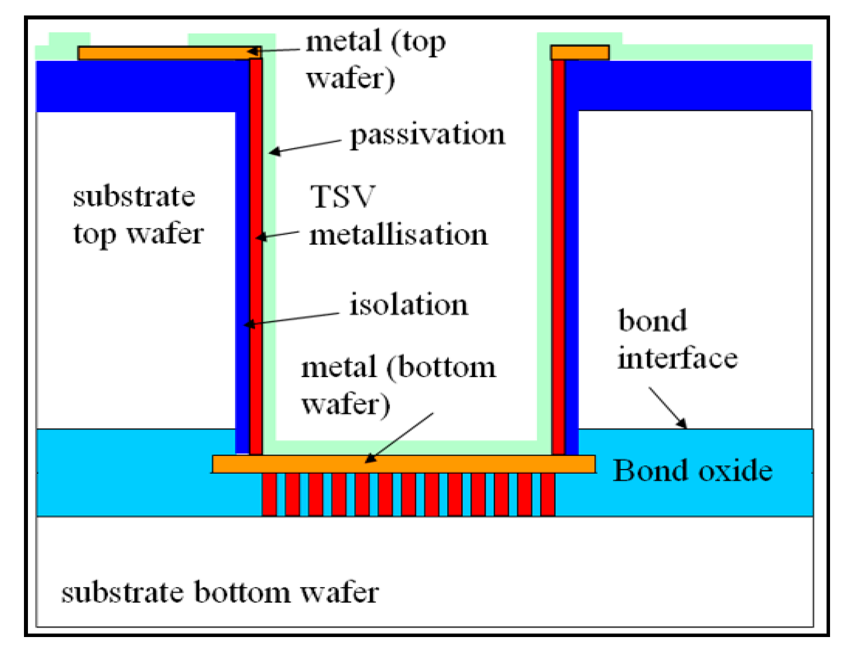
Figure 18.
TSV Substrate.
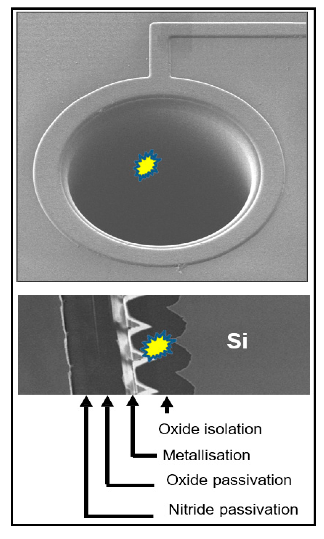
Figure 19.
Principle of inverted Electron Beam Absorbed Current (EBAC) image used to overlay EBI image and detect a defect.
Figure 19.
Principle of inverted Electron Beam Absorbed Current (EBAC) image used to overlay EBI image and detect a defect.

Figure 20.
Revolutionary five columns technology to increase the throughput.

Figure 21.
Multi-beam Scanning Electron Microscopes (SEM) principle using multi-beam in parallel to image a hexagonal sample area 100 micron wide. Primary electrons (solid lines, left) are focused onto the specimen & separated by a beam splitter from the secondary electrons (dotted lines, right).
Figure 21.
Multi-beam Scanning Electron Microscopes (SEM) principle using multi-beam in parallel to image a hexagonal sample area 100 micron wide. Primary electrons (solid lines, left) are focused onto the specimen & separated by a beam splitter from the secondary electrons (dotted lines, right).

Figure 22.
Applied Materials PROVision e-beam.
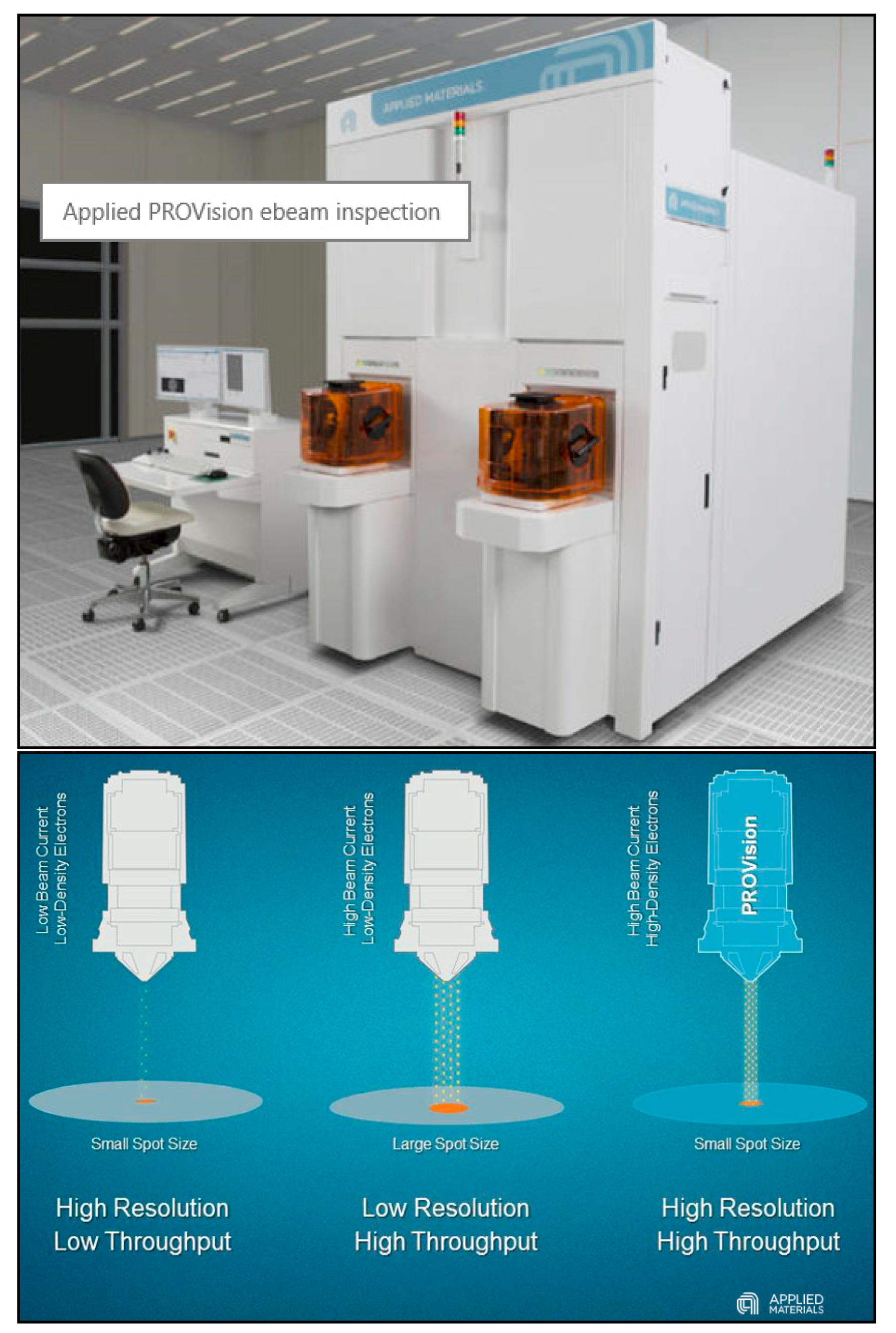
Figure 23.
Applied Materials PROVision e-beam’s capability.

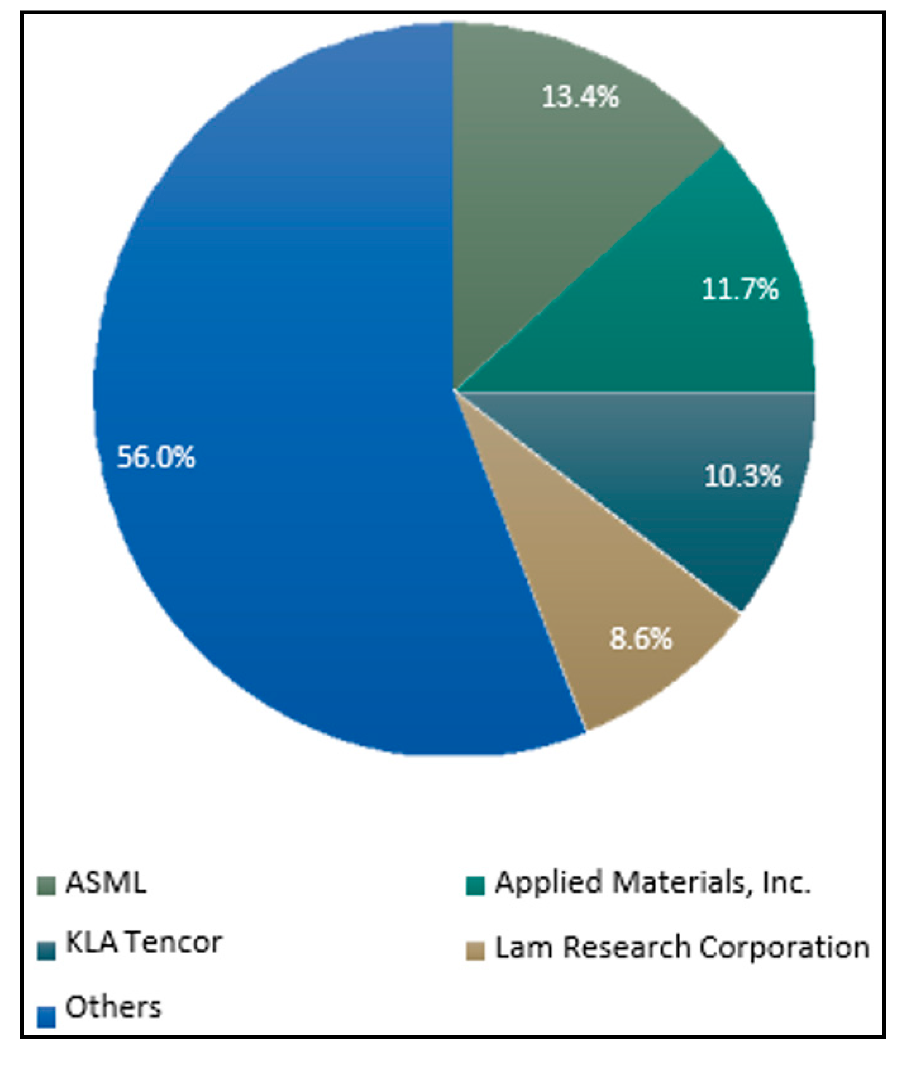
Figure 24.
Global e-beam Wafer inspection system market share.

Figure 25.
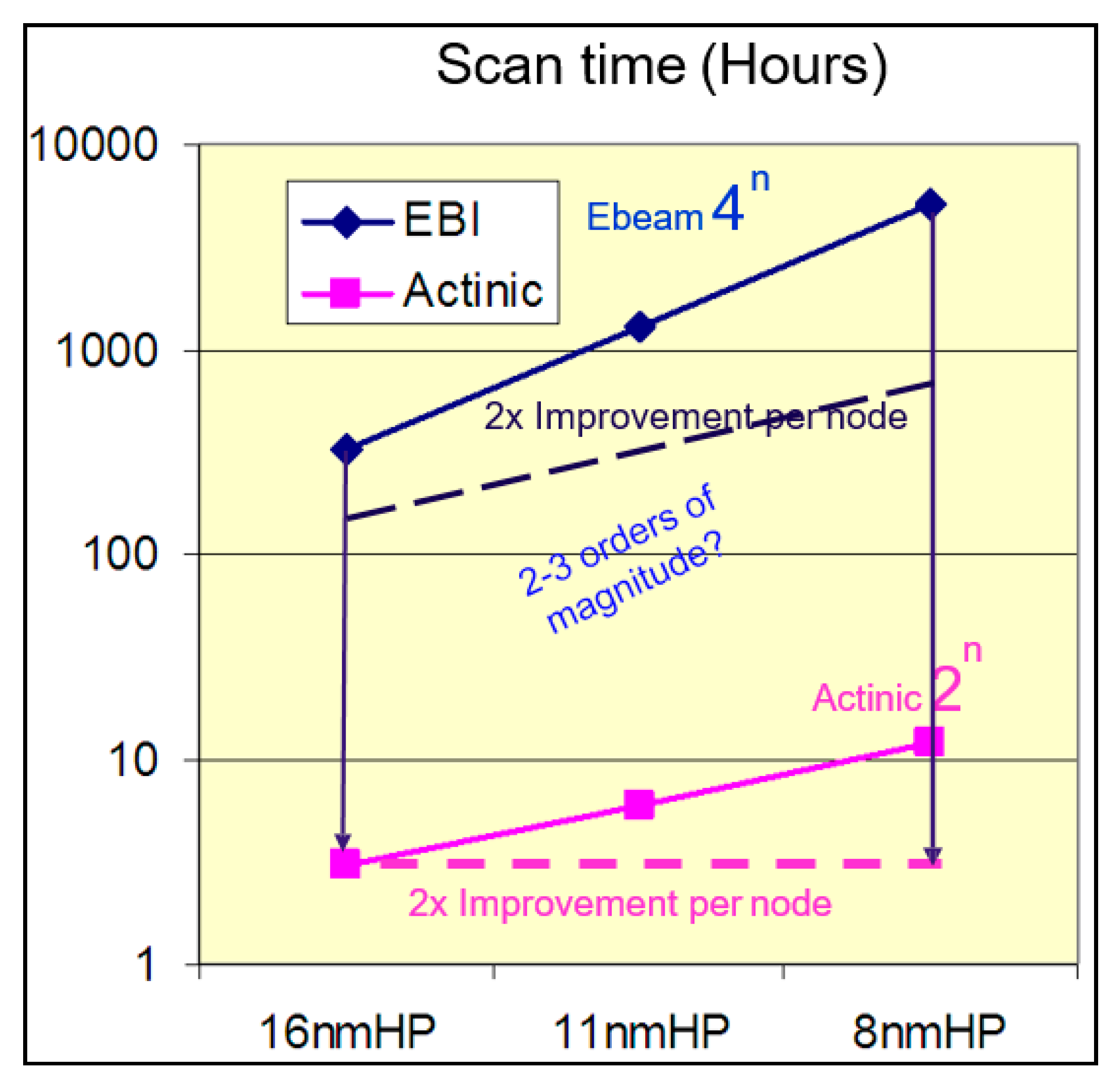
Scan time comparison.

Figure 26.
Throughput versus sensitivity distribution of various design node.
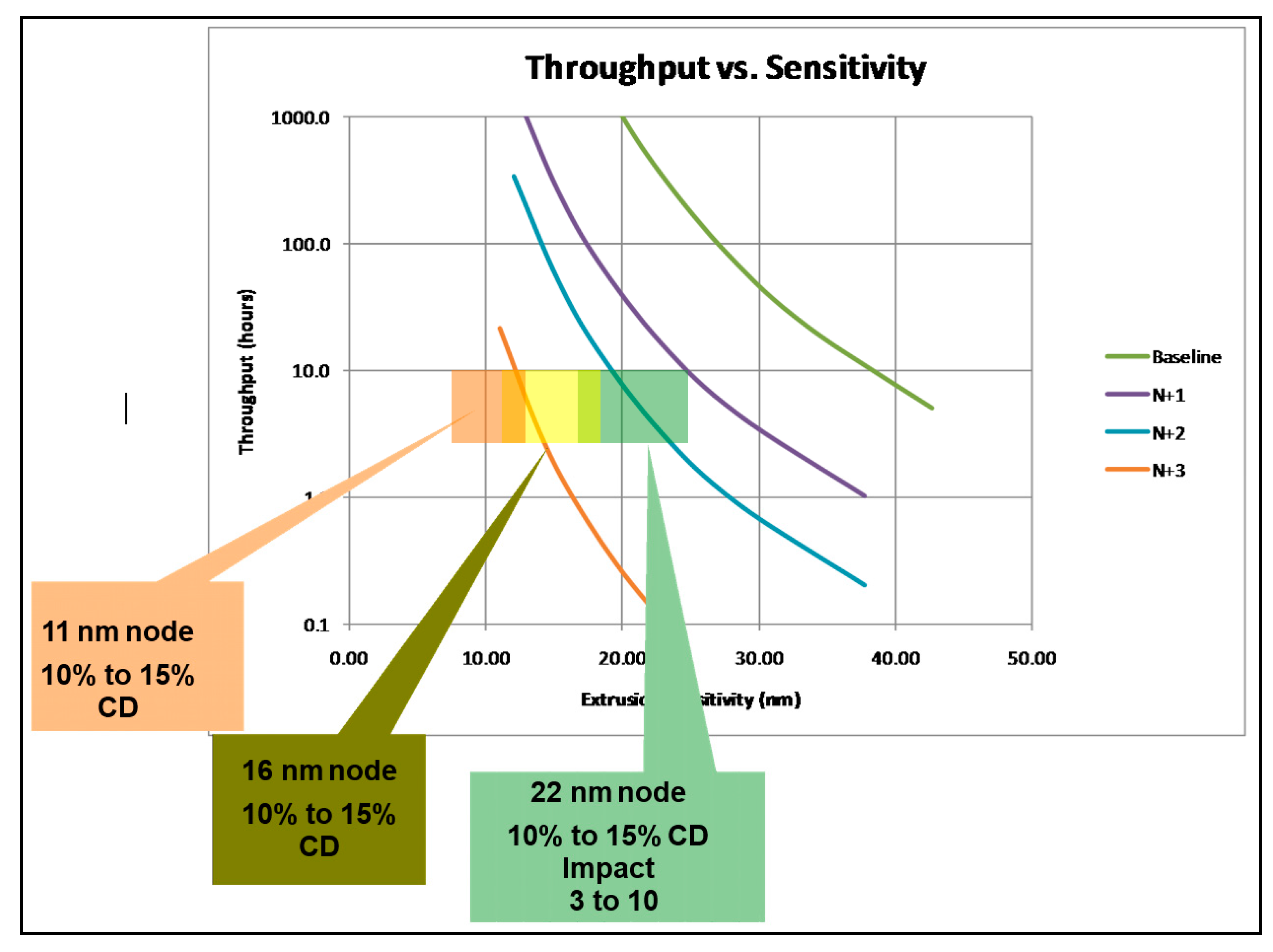
Figure 27.
Logic technology roadmap and alternatives for key components with timing for critical decision points.
Figure 27.
Logic technology roadmap and alternatives for key components with timing for critical decision points.
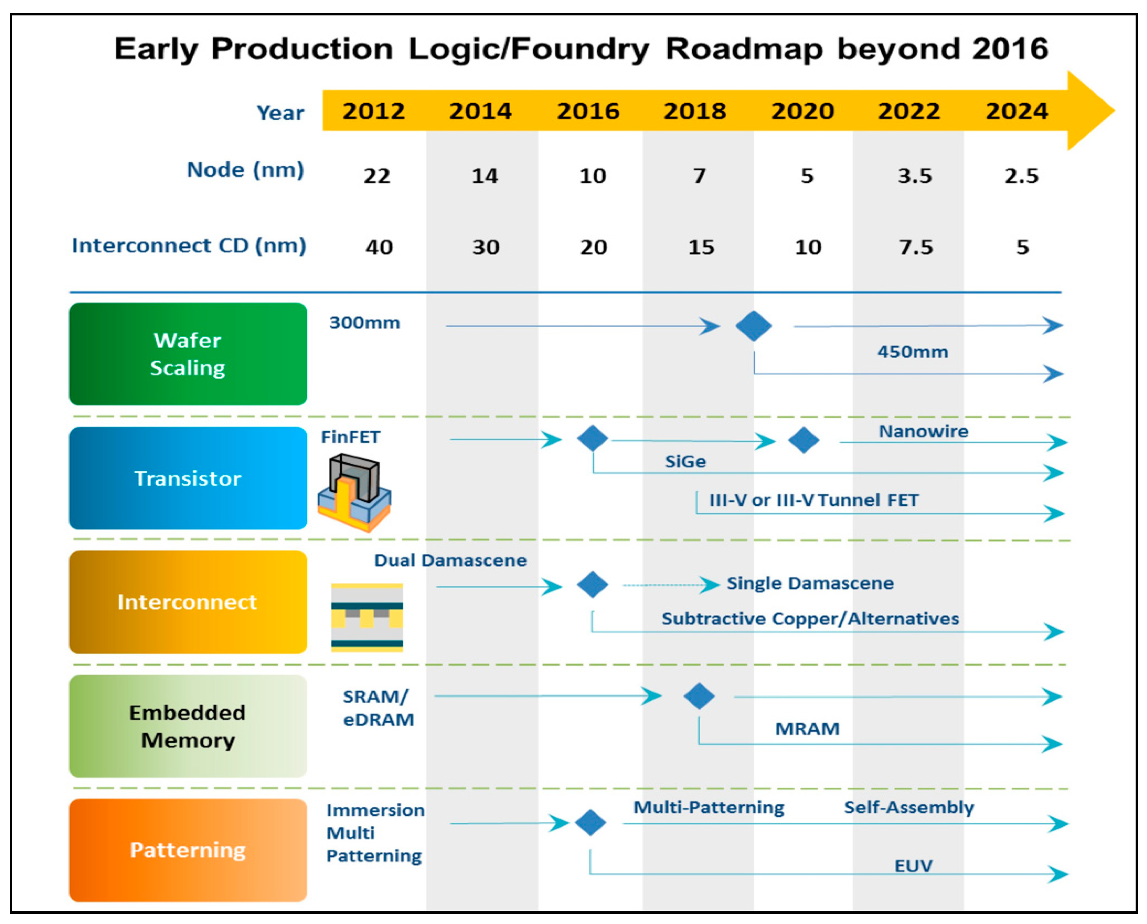
Figure 28.
Various nodes and related technology fulfillment.
Figure 29.
Global share analysis.

Figure 30.
Global E-beam wafer inspection system market value share analysis by application, 2016–2025.
Figure 30.
Global E-beam wafer inspection system market value share analysis by application, 2016–2025.
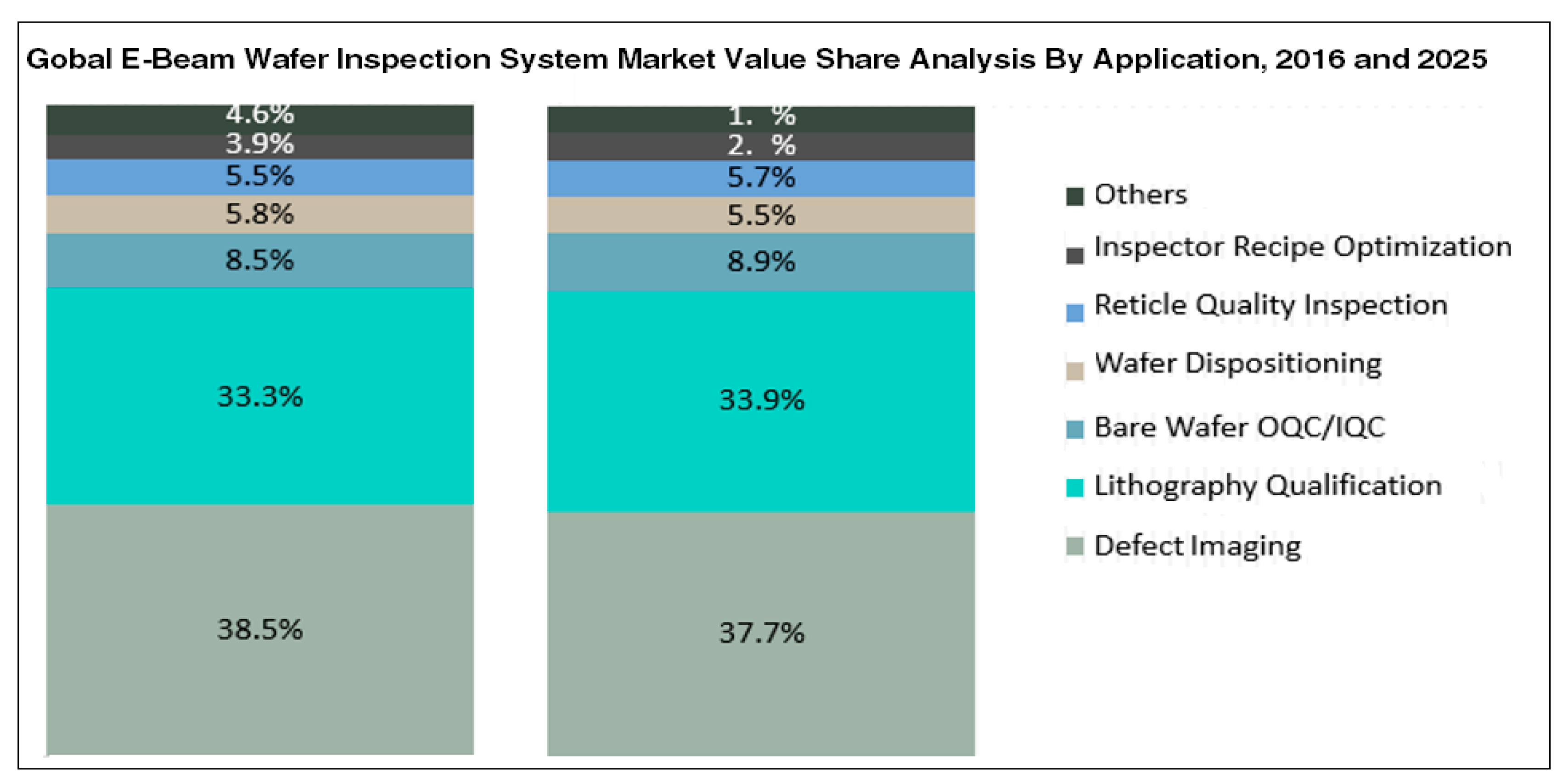
Figure 31.
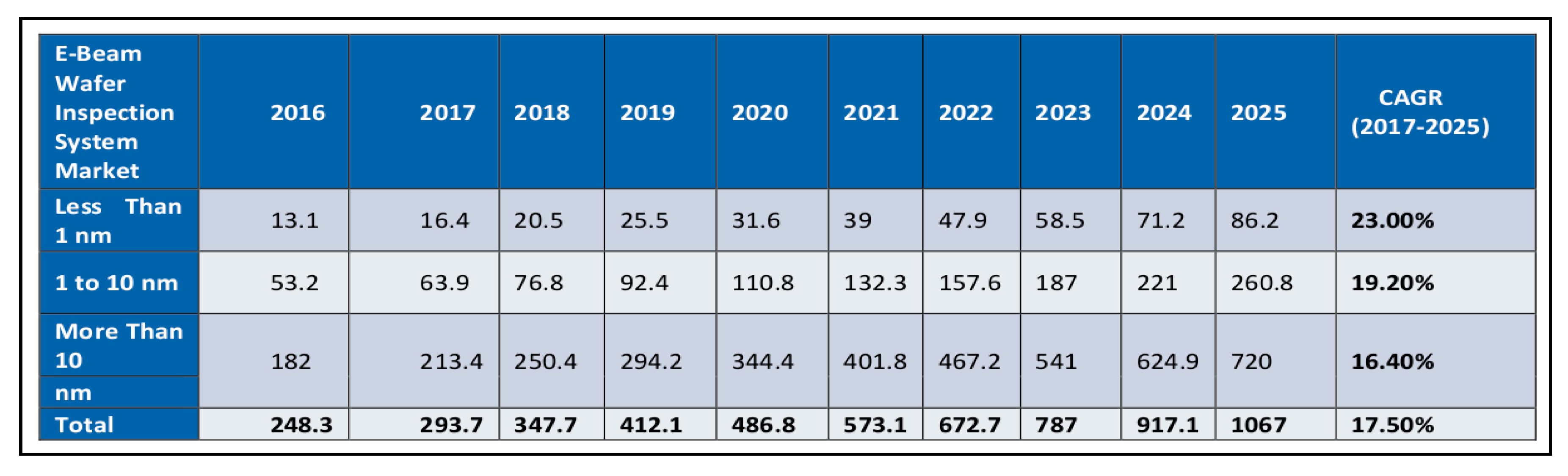
Global e-beam wafer inspection system market size (USD Mn) forecast by type, 2016–2025.

Table 1.
E-Beam versus optical tool.
| Parameters | Optical Inspection | e-Beam Inspection |
|---|---|---|
| Defects Capability | Physical defects | Smaller physical defects and electrical defects |
| Performance | Fast | Slow |
| Scan area | Large area (complete wafer) | High |
| Market share | ~86% | ~14% |
| Majorly used at | Production (in-line) | Research and Development (R&D) |
| Resolution | Medium | High |
Table 2.
Typical Single Column Multiple Beam Parameters and their Values.
| Parameter | Value |
|---|---|
| Typical landing energies of the multi-beam electron microscope | 1–3 keV |
| Typical pixel sizes | 4–10 nm |
| Distance between two electron beams | 12 μm |
Table 3.
Comparison of Technologies.
| Future Technology | Projection e-Beam | Multiple e-Beam | Multi-Column Multi-Objective Lens | Multi-Column Single Objective Lens |
|---|---|---|---|---|
| Pros | High scan rate | With-in full die application | Easy control symmetry beam | Small volume |
| Cons | Interaction high, low SNR, low resolution | Asymmetrical control, non-uniform | Large volume | Asymmetrical control |
| Resolution | Moderate | Moderate | High | High |
| Throughput | Fastest | Faster | Fast | Faster |
Table 4.
Scan time comparison.
| Scan Time | 16 nm | 11 nm | 8 nm |
|---|---|---|---|
| EBI (Pattern only) | 320 h (2 weeks) | 1280 h (8 weeks) | 5120 h (30 weeks) |
| Actinic (Blank and Pattern) | 3 h | 6 h | 12 h |
© 2017 by the authors. Licensee MDPI, Basel, Switzerland. This article is an open access article distributed under the terms and conditions of the Creative Commons Attribution (CC BY) license (http://creativecommons.org/licenses/by/4.0/).
Share and Cite
MDPI and ACS Style
Oberai, A.; Yuan, J.-S. Smart E-Beam for Defect Identification & Analysis in the Nanoscale Technology Nodes: Technical Perspectives. Electronics 2017, 6, 87. https://doi.org/10.3390/electronics6040087
AMA Style
Oberai A, Yuan J-S. Smart E-Beam for Defect Identification & Analysis in the Nanoscale Technology Nodes: Technical Perspectives. Electronics. 2017; 6(4):87. https://doi.org/10.3390/electronics6040087
Chicago/Turabian StyleOberai, Ankush, and Jiann-Shiun Yuan. 2017. "Smart E-Beam for Defect Identification & Analysis in the Nanoscale Technology Nodes: Technical Perspectives" Electronics 6, no. 4: 87. https://doi.org/10.3390/electronics6040087
Note that from the first issue of 2016, this journal uses article numbers instead of page numbers. See further details here.