Electromagnetic Characterisation of Materials by Using Transmission/Reflection (T/R) Devices


Dipartimento di Ingegneria dell’Informazione, Università di Pisa, 56126 Pisa, Italy
*
Author to whom correspondence should be addressed.
Electronics 2017, 6(4), 95; https://doi.org/10.3390/electronics6040095
Submission received: 1 October 2017
/
Revised: 28 October 2017
/
Accepted: 7 November 2017
/
Published: 9 November 2017
Abstract
:An overview of transmission/reflection-based methods for the electromagnetic characterisation of materials is presented. The paper initially describes the most popular approaches for the characterisation of bulk materials in terms of dielectric permittivity and magnetic permeability. Subsequently, the limitations and the methods aimed at removing the ambiguities deriving from the application of the classical Nicolson–Ross–Weir direct inversion are discussed. The second part of the paper is focused on the characterisation of partially conductive thin sheets in terms of surface impedance via waveguide setups. All the presented measurement techniques are applicable to conventional transmission reflection devices such as coaxial cables or waveguides.
1. Introduction
Recent technological advances have fostered the use of new materials and composites in several different fields spanning from electronics to mechanics, agriculture, food engineering, medicine, etc. Two-dimensional materials [1] have attracted considerable interest from the electronic devices community. Graphene is probably the foremost representative of that class of materials and promises a revolution in many applications. It has also aroused the interest of the scientific community towards other two-dimensional, or quasi-2D, materials, which are receiving increasing attention thanks to the development of printable electronics technology, which allows fast and low-cost prototyping and fabrication of device like antennas [2,3,4], periodic surfaces [5,6], or sensors and tags [7,8,9]. Those kinds of application require highly conductive inks that may exhibit high losses, which, in turn, can be exploited for the design of absorbing materials [10,11,12,13,14,15] and for electromagnetic signature control [16]. The applicability of these techniques has been recently pushed to above 100 GHz using reverse offset (RO) printing, which allows high line-resolution and increases printing speed [17,18]. Microwave properties of materials are also of crucial importance for the development of electronic and flexible circuits working at microwave frequencies: flex circuits [19,20,21,22] are often adopted in computer peripherals, cellular phones, cameras, printers, and LCD fabrication. The film deposited on top of the substrate exhibits a thickness of a few micrometres.
That plethora of new materials and their innovative applications represent a driver for the development of new and more accurate techniques to characterise their electromagnetic properties. However, the measurement of thin materials is still a challenge. Unambiguous and precise characterisation of specimens over a very wide band is increasingly important. Non-destructive testing (NDT), which is fundamental in science and technology for the screening of components or systems without damaging or permanently altering the sample, can find a natural solution in the electromagnetic techniques for the material’s properties measurement. Free-space reflection and open-ended probe techniques are typical transmission/reflection or reflection-only NDT methods [23,24,25,26,27,28]: they are indeed attractive because they maintain material integrity and are increasingly used in various fields (mechanics, constructions, medicine, and so on), but they usually pay a price in terms of accuracy and mathematical model complexity with respect to the guided T/R methods.
In this context, it is fundamental to have access to methodologies able to accurately characterise the properties of materials. A number of those techniques are available in the scientific literature [29,30]. They can be substantially divided into two categories: resonant methods and transmission/reflection (T/R) methods. In the former case, very accurate electromagnetic (EM) characterisation is achievable but requires the precise fabrication of both the measured sample and the designed resonator [29]. In addition, these methodologies are often customised for a reduced set of materials (range of measured dielectric permittivity and magnetic permeability, size and physical state of the sample). Unfortunately, this approach can be impractical and expensive for research laboratories, where, usually, the characterisation of materials is not the focus of the working activity but a preliminary step towards the design of an electronic or electromagnetic device. In the latter case, commercial T/R devices, such as coaxial cables, waveguides or even free space propagation, can be employed to perform the characterisation of materials. Unlike the methods, which are based on single-frequency or multiple-frequencies measurements, the T/R characterisation is intrinsically wideband. The frequency band in which the characterisation is valid depends on the specific T/R device and on the employed equipment. In both cases of coaxial cables and waveguides, the material is characterised in the unimodal propagation band of the device. In addition, coaxial cables offer a wider bandwidth and allow one performing (at least in theory) the measurement at low frequency since they do not have a cut-off band. However, since this measurement technique requires that the shape of the material be adapted to the concentric corona of the cable, the manufacturing of the sample is not straightforward. On the contrary, the preparation of the sample for waveguides is much simpler, thus justifying the success of waveguides over the coaxial cables even at the cost of a smaller allowed bandwidth.
The purpose of this paper is to present an overview of T/R-based methods for the characterisation of a large set of materials by employing standard laboratory measurement equipment. Electric and magnetic polarisations effects of materials are macroscopically described by two well-known parameters, namely the dielectric permittivity and the magnetic permeability. A summary of the methods presented in the paper is displayed in Figure 1. In the second section, the most well-known T/R characterisation procedure for retrieving dielectric permittivity and magnetic permeability of materials, the Nicholson–Ross–Weir [31,32] method (NRW), is presented. The method is easy to use as it allows for retrieving the dielectric permittivity and magnetic permeability from the measured scattering parameters of the unknown sample through a simple analytic procedure. However, the NRW approach presents a number of limitations that have been extensively discussed in the literature [33,34,35], and a number of alternative procedures have been proposed throughout the years [35,36,37,38,39]. The most relevant limitations of the method and some of the most remarkable approaches aimed at overcoming the NRW drawbacks will be presented, with examples. Specifically, particular attention will be dedicated to the possible ambiguities in the determination of the dielectric permittivity and magnetic permeability, which arise in the direct inversion procedure typical of the NRW algorithm [40,41,42]. It will be shown that these limitations can be circumvented by treating the inversion problem as a global optimisation procedure, where only solutions obeying to causal models of materials (Lorentz or Debye models) are searched by using an iterative procedure. This approach will be called Baker–Jarvis (BJ) method [36]. Another useful technique to characterize the dielectric properties of thin low-dielectric permittivity materials based on resonant FSS filters in waveguide environment will also be discussed [43]. The third section is dedicated to the characterisation of thin two-dimensional materials with non-negligible conductivity. Moreover, the cases where the sheet impedance approximation is valid will be discussed. If the sheet impedance condition is verified, the 2D material can be characterised in terms of complex sheet impedance instead of using bulk parameters such as the complex dielectric permittivity. Afterwards, a characterisation approach employing the same waveguide experimental setup [44,45,46] to derive the surface impedance of the sample is presented.
2. Measuring Properties of Dielectric Materials
The electromagnetic characterisation of dielectric materials is a relevant aspect in numerous practical applications. Over the years, several experimental techniques aimed at extracting the dielectric properties of a materials have been investigated [29,30]. The choice of the EM characterisation method depends on the EM parameters such as the frequency band and the required accuracy of the results and, more remarkably, also on the physical and mechanical parameters of the investigated specimen such as its physical state (solid, liquid), its size and shape. In addition, a priori information regarding the nature of the analysed material is needed. For example, resonant methods provide reliable results for dielectric materials with low losses. These methods, which employ resonant structures such as cavity resonators, rely on the measure of the Q-factor and the resonance frequency of the cavity. Alternatively, non-resonant methods, which employ transmission lines, rely on the measure of the signal reflected and transmitted by the specimen under test. While resonant methods are able to accurately characterise the material over a discrete number of frequencies, non-resonant methods inherently provide broadband results. In addition, non-resonant methods can be applied to different measuring setups. Although coaxial line probes require a very accurate shaping of the sample, they can measure EM properties of the material over a very wide band and, in theory, at low frequencies. Waveguide methods are usually more popular since circular or rectangular samples are easier to produce than coaxial ones. However, waveguide-based estimations are only valid over a limited frequency range. On the other hand, free-space techniques not only circumvent the problem of the sample fit precision but also preserve the integrity of the sample (non-destructive). A major disadvantage of the free-space method is that, in order to avoid diffraction effects due to sample edges, the wireless measurement of the scattering parameters through antennas requires a sample of several wavelengths.
2.1. Nicolson–Ross–Weir Procedure
One of the most popular procedures for the EM characterisation of materials is the Nicolson–Ross–Weir (NRW) method, based on T/R measurements of the specimen under test. The properties of materials are retrieved from their impedance and the wave velocities in the materials. It is well known that the main drawback of this method is related to the electrical thickness of the analysed material [40]. In particular, when the thickness of the specimen is an integer multiple of half wavelength in the material, the method produces ambiguous results due to the 2π periodicity of the phase of the EM wave. In principle, from a priori information regarding the specimen, it is possible to achieve unambiguous results. In addition, as will be presented in this section, because of the inversion procedure adopted for the extraction of the EM parameters, the NRW method is not accurate in the case of low reflecting materials or thin samples. Two examples of transmission lines for the material characterisation are reported in Figure 2. The sample under test with thickness d is located inside a two-port microwave device such as a coaxial cable (Figure 2a) or a waveguide (Figure 2b).
Due to the presence of a sample of thickness d, the phase factor (T) due to phase delay, (T) can be defined as:
The reflection coefficient at the first interface between the transmission line’s sections with and without the specimen is defined as:
where Z0 and Z1 are the transmission line’s characteristic impedances in absence and in the presence of the sample, respectively. The expression of Z1 can be straightforwardly derived from Equation (2) as follows:
According to the theory of multiple reflections [31], the scattering parameters of the finite length sample (S11 and S21) can be written as a function of the reflection coefficient at the interface of two infinite media Γ and as a function of the phase factor T:
At this point, the reflection coefficient Γ, which contains the impedance of the unknown medium, and the phase factor T, which contains the propagation constant of the unknown medium, can be expressed as a function of the scattering parameters of the sample:
where the auxiliary parameter K is a function of the scattering parameters S11 and S21:
As it is apparent in Equation (5), the reflection coefficient Γ is characterised by a sign ambiguity. The sign should be properly chosen to obtain the correct impedance and propagation constant of the medium [47,48] (passivity condition), which can be verified at the end of the inversion procedure. However, if one needs to estimate only the dielectric permittivity and the magnetic permeability of the medium, both signs can be arbitrarily chosen. Indeed, since the dielectric permittivity and the magnetic permeability are a product of the impedance of the medium and its propagation constant, the correct sign is always restored [40].
The phase factor T of relation (1) can be expressed with its amplitude |T| and a phase term φ as follows:
Consequently, the propagation constant γ can be obtained by applying the natural logarithm of the complex variable T. The natural logarithm of the complex variable T will be complex. Its real part can be expressed as the logarithm of its amplitude and the imaginary part will be the phase term φ plus a 2π phase ambiguity:
It is evident from Equation (8) that there is an ambiguity in the calculation of γ because of the term 2πn. The existence of an infinite number of valid solutions is called branching. Therefore, in order to solve this ambiguity, the NRW method requires a thin specimen material (usually a quarter of a wavelength) so that n = 0 at the analysed frequencies.
Once γ is calculated, it is possible to estimate the electrical permittivity and the magnetic permeability:
In a waveguide environment [32], the magnetic permeability can be similarly calculated by using the equivalent transmission line circuit of the waveguide:
where k0 is the propagation constant in free space and kt is the cutoff wavenumber of the waveguide. On the contrary, the dielectric permittivity should be derived from the propagation constant after the derivation of the magnetic permeability:
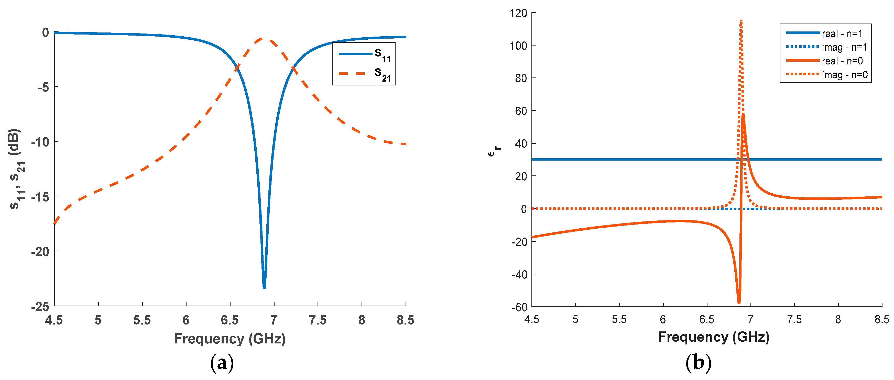
An example of an application of the NRW procedure for the characterisation of a dielectric material is reported hereinafter. A material sample with thickness equal to 8 mm and εr = 9 − j0, µr = 1 − j0 is considered. The transmission and reflection coefficient simulated with a transmission line model are reported in Figure 3.
The application of the NRW with n = 0 provides the results reported in Figure 4a,b. As is evident from the graphs displayed in Figure 4, when the thickness of the sample is equal to half a wavelength in the dielectric media (λg/2) the NRW method produces ambiguous results. In this particular case, the thickness of the sample is equal to λg/2 at 6.4 GHz:
As reported in Figure 4, the results obtained with n = 0 are valid up to 6.4 GHz, where the estimated parameters are constant. Similarly, with n = 1, the results are valid starting from 6.4 GHz. Therefore, it is evident that with this formulation of the NRW method the user needs to choose the valid results depending on the different values of n. In order to overcome the limitations of the branch point selection, a stepwise scheme of the NRW method has been proposed [38]. The procedure is based on the fact that the measured sample is thinner than half-guided wavelength at the lowest frequency.
Therefore, the n = 0 branch is selected at the lowest measured frequency:
The argument of the propagation constant for the subsequent frequency point p is selected using a step-by-step increment, which avoids the selection of the branch value n:
The real and imaginary parts of the propagation constant characterised with the NRW (n = 0) and stepwise method are reported in Figure 5a,b, respectively.
If the sample is not thinner than a half-guided wavelength at the lowest frequency, unphysical solutions are also obtained using the stepwise method. This case can be analysed considering a sample with thickness d = 8 mm and εr = 30 − j0.2, µr = 1 − j0. The scattering parameters S11 and S21 and the real and imaginary part of the dielectric permittivity estimated with the stepwise method when n = 0 and n = 1 are reported in Figure 6a,b, respectively. As is evident from Figure 6b, unphysical values of the dielectric permittivity are provided by the stepwise method when n = 0.
The NRW direct inversion procedure is sensitive to the inaccuracies of the S-parameters at the N*λg/2 resonances, with N entire number. Indeed, at that frequency, the sample becomes a half-wavelength window and the reflection coefficient tends to zero. Consequently, it is not possible to apply the direct inversion procedure. Moreover, in the case of noisy measurements, this method will induce a high uncertainty in the extracted parameters of the material and may cause problems in finding the correct branch in the vicinity of these frequencies [49].
As an example, a material characterised by a constant dielectric permittivity (εr = 9 − j0.2) and a thickness of 9 mm simulated in a waveguide environment (WR137 waveguide) is analysed. The synthetic scattering parameters are perturbed with Additive White Gaussian Noise (AWGN) characterised by a mean value (mv) equal to zero and standard deviation (σ) equal to 0.01. As is shown in Figure 7, the application of the NRW formulas leads to high inaccuracies around 6.4 GHz where the reflection coefficient of the samples is very low. The estimation error depends on the accuracy of the available scattering parameters. In [50,51], the Cramér–Rao lower bounds, that is, the minim variance achievable with a fixed SNR of the measured scattering parameters, are derived. Using these bounds, it is possible to estimate the minimum Signal to Noise Ratio (SNR) required to estimate the material parameters with a given accuracy.
Finally, it is worth mentioning that several variations of the original formulation of the NRW method have been proposed in the literature. Several approaches to improve the stability of the results with “noisy” or not enough accurate data when the sample is thin, or the material exhibits a low reflectivity have been presented [52,53,54]. Moreover, formulations able to make the characterisation of the material independent of the calibration planes have been also studied [54,55]. Finally, some techniques based only on measured reflection or transmission amplitude have been also investigated [56,57].
2.2. Iterative Non-Ambiguous Estimation of Dielectric Permittivity from Broadband Transmission/Reflection Measurements
The extraction of the dielectric constants from T/R measurements can be ambiguous when the S-parameter inversion is performed frequency-by-frequency. The reason is the impossibility of determining the correct branch of the solution with any initial guess of the material properties. High values of permittivity or permeability might lead to a sample with an electrical thickness of several multiples of half-wavelengths, even at the lowest measurement frequency. Consequently, the choice of the ambiguity integer n in (13) is not straightforward. This is particularly true when the NRW inversion algorithm is applied to metamaterials where the permittivity and permeability tensor values are dispersive with frequency and they can rapidly increase in certain frequency bands around the resonances [42,47,49,58,59,60]. One of the main problems of the NRW direct inversion procedure is that it admits unphysical non-causal solutions [41,49]. An alternative approach that exploits the correlation among contiguous frequency points, thus circumventing the ambiguity and discontinuity problems that plague the NRW method, was presented by Baker Jarvis in 1992 [36]. The best estimation of the dielectric permittivity can be obtained with an iterative fitting of an objective function, which minimises the quadratic errors on the magnitude and phase of S-parameters among the predicted and measured data. The method does not require any initial guess on the permittivity and may search the best estimation on the whole complex permittivity domain. Moreover, the algorithm can be successfully employed both with T/R or R measurements [61].
The idea of the iterative method is to search only physical solutions analysing the scattering parameter over all the available frequency points at the same time. In this way, it is possible to exploit the correlation among frequency points, which is instead neglected by the NRW method. The scattering parameters of a sample transversally placed in a T/R device can be analytically retrieved by using a simple transmission line model [44,62,63].
Therefore, the unknown permittivity and permeability profiles can be estimated by computing the discrepancy between the measured scattering parameters and the analytically estimated ones based on physical permittivity models. The discrepancy can be estimated by using the following cost function:
where , are the measured scattering parameters at the frequencies of interest fn and are the S parameters estimated according to the transmission line model.
The cost function FC, which is reported in terms of real and imaginary part in the Formula (16) equation reference goes here, can also be expressed in terms of amplitude and phase, as follows:
In the simplest case of a dielectric sample with constant permittivity parameters, only the real and the imaginary part of the dielectric constant needs to be estimated and a two-dimensional space is analysed. However, in the presence of noise, the cost function is not convex and exhibits local minima. Consequently, a single starting point is not sufficient for the analysis, especially when the number of unknown parameters increases. Unfortunately, without an initial guess of the sample, a very large range of possible values of the unknown parameters needs to be explored. For this reason, a certain number of initial values have to be chosen initially. It is obvious that, in order to explore the two-dimensional space with a reasonable computation time, a coarse sampling is recommended. Let us select a set of initial points and apply an iterative line-search gradient algorithm for every initial point in order to exhaustively explore the surrounding space. Given a starting point , the algorithm refines the permittivity values by moving on the steepest descent path:
where the subscript m individuates the convergence step and:
If the new computed cost function respects the condition , the next value of the complex dielectric permittivity is retained. Otherwise, the multiplying coefficient is halved and the iteration is repeated as follows:
The algorithm converges when the following condition is fulfilled:
The algorithm for the simple 2D space is very fast since the formulation is based on an analytic solver. In case of good estimation, the cost function will decrease towards zero. Moreover, for a further speed-up of the algorithm, the measured data can be under-sampled. In addition, the estimation of the magnetic permeability can be easily included in the method by enlarging the initial explored space up to four dimensions. The presented iterative procedure will be applied to different dielectric materials hereinafter.
The first numerical example is a specimen of 0.1 m with a relative dielectric permittivity εR = 20 − j10. The sample is considered transversally accommodated in coaxial cable and measured in the band 100–500 MHz over 50 frequency samples. In this preliminary analysis, the target scattering parameters are synthetically generated by using the equivalent transmission line model. The complex space of the dielectric permittivity is sampled over nine points uniformly distributed between 0 and 50 for the real part and over 0 and 250 for the imaginary part. The initial and final positions provided by the iterative algorithm for each starting point are shown in Figure 8a. As is evident from Figure 8a, the algorithm converges to the same value for every starting point. If the same approach is applied to a sample of 0.2 m characterised by a relative dielectric permittivity εR = 6.15 − j0.0184 in the frequency range 100–500 MHz, not all the starting points of the complex space converge to the correct solution (Figure 8b). Finally, it is worth underlining that the proposed method does not suffer the ambiguities of phase extraction from transmission coefficient that affect the classical NRW algorithm. In fact, if the NRW inversion procedure is applied to the synthetic data of the second example, divergent solutions are obtained when the sample length is equal to or longer than a half wavelength. On the contrary, the proposed method is stable on the whole bandwidth, thus proving its broadband applicability.
It is worth highlighting that, if general and realistic dielectric permittivity and magnetic permeability models are selected, the number of parameters to be found increases with respect to the case of constant values. On the contrary, by recurring to causal models for the sample under testing, the dielectric permittivity and the magnetic permeability of a material can be characterised using only a few parameters. The most important models, widely adopted to describe the dielectric behaviour of materials, are provided by Lorentz and Debye. In this case, the iterative search consists of optimising the parameters of the causal models by matching the measured scattering parameters with those obtained from the simulations of the material. We will address this method as Backer–Jarvis (BJ) since a similar approach was presented by the author [36].
The definition of the employed causals models is provided hereinafter. According to the Lorentz model, the electrons are considered as damped harmonically bound particles subject to the external field. Lorentz’s model relies on the fact that the mass of the nucleus of the atom is much higher than the mass of the electron. Consequently, the problem can be treated as an infinite mass connected to an electron-spring system. In addition, the hypothesis that the biding force can be modelled as a spring, can be considered valid for any kind of binding because of the small displacement. The permittivity provided by Lorentz’s model can be written as follows:
In this formula, and are the static dielectric constant and the optic region permittivity, respectively. The parameter f0 is the resonance frequency, Δf is the width of the Lorentzian resonance line at the –3 dB level, and the term is the relaxation frequency parameter.
The Debye model describes the properties of polar dielectric materials. It can be interpreted as a special case of the Lorentz model when the displacement vector is replaced by the dipole rotation angle 𝜃 (i.e., the angle between the dipoles and the excitation E field).
The rate at which polarisation can occur is limited: as the frequency of the external EM field increases, the dipole moments are not able to orient themselves fast enough to maintain alignment with the excitation and the total polarizability decreases. This fall, with its related reduction of permittivity and the occurrence of energy absorption, is referred to as dielectric relaxations or dispersions.
The relaxation mechanism in dipolar dielectric materials is described by the Debye model:
The real and imaginary part as a function of the frequency of the electric permittivity in the case of the Debye (a) and Lorentz (b) models are reported in Figure 9a,b, respectively. It is worth underling that, in the iterative process, five parameters need to be estimated for Lorentz’s model. These parameters are highlighted in Figure 9b. Similarly, the estimation of four parameters is required for Debye’s model, as reported in Figure 9a.
Real materials might exhibit several resonances, which can be characterised as a combination of multiple Lorentz and Debye terms as follows:
As is evident from Equation (23), if a material can be modelled with N Lorentz resonances and M Debye resonances, the total number of parameters (Tp) to estimate is equal to:
In order to improve the convergence of the algorithm, since the dimension of the solutions space increases with the complexity of the employed model, the iterative method can be implemented with a genetic algorithm (GA) instead of the iterative gradient technique. The iterative approach employing the Debye model is compared with the NRW method by analysing the case of a dielectric sample of thickness equal to 10 cm with μr = 1. The geometrical and electrical parameters are summarised in Table 1.
As is evident from Figure 10a, both the NRW and the iterative method accurately estimate the real and imaginary parts of the dielectric permittivity (continuous line). Conversely, when the thickness of the same dielectric sample is 15 cm, the NRW method is not able to correctly estimate the dielectric permittivity (Figure 10b). Indeed, the NRW method fails to retrieve the dielectric permittivity and magnetic permeability if n = 0 is not suitable for the first point of the frequency window. On the other hand, the iterative method accurately estimates both the real and imaginary parts of the dielectric permittivity. The optimisation is performed using a GA. Clearly, the smaller the space where the solution is searched, the closer will be the found solution. In the case reported in Figure 10, the GA is run three times before selecting the best solution. Every run of the GA lasts 20 s, thus obtaining an overall optimisation time equal to one minute. The results provided by the NRW and iterative method have also been analysed for the case of noisy input data. In particular, S11 and S21 obtained from the measurement of a dielectric sample with μr = 1 and thickness equal to 10 cm have been corrupted with Additive White Gaussian Noise (AWGN) with a mean value (mv) equal to zero and standard deviation (σ) equal to 0.01. The measured and noisy S-parameters are reported in Figure 11a. As it is apparent from Figure 11b, the Baker–Jarvis (BJ) iterative method is robust with respect to the AWGN, thus providing an accurate estimation of the real and imaginary part of the dielectric permittivity.
The NRW and the BJ iterative methods have also been compared in the case of noisy data for the estimation of both dielectric permittivity and magnetic permeability. The input S-parameters are obtained from a material sample of 10 cm characterised by the same electrical parameters summarised in Table 1, except that μr = 3. The S-parameters have been corrupted with AWGN (mv = 0, σ = 0.01). The real and imaginary parts of the dielectric permittivity estimated with NRW and the iterative method employing the Debye dispersion model are reported in Figure 12a.
From Figure 12a, we note that the iterative method is sufficiently accurate whereas the NRW method provides unphysical results since the electrical length of the sample exceeds a half wavelength at the lowest investigated frequency. Conversely, for the NRW method the estimation of the magnetic permeability is critical (Figure 12b), whereas the iterative method provides accurate results.
The main advantages and disadvantages of the two approaches for retrieving the dielectric and magnetic properties of the materials are summarised in Table 2.
2.3. FSS-Based Waveguide Resonant Method
Resonant methods usually exhibit higher accuracies and sensitivities than non-resonant methods, and they are more suitable for low-loss samples. Resonant methods are based on the property that the resonant frequency and quality factor of a dielectric resonator with given dimensions are determined by its permittivity and permeability. These methods are usually employed for the characterizsation of low-loss dielectrics with permeability equal to μ0. There are a large number of resonant methods for the estimation of the dielectric properties of materials [29] but they usually require ad hoc cavities and a direct etching of the resonator on the unknown sample. The preparation of the sample under test can be a difficult task in cavity perturbation techniques, as the sample requires a regular geometry. In resonant methods, the sample permittivity is evaluated from the shift of the resonant frequency. All the resonant methods are limited to either a specific frequency range, some kinds of materials, or specific applications.
A simple resonant method employable in a waveguide environment was proposed in [43]. It adopts a waveguide—which is a common transmission/reflection device—in conjunction with a resonant device, a planar Frequency Selective Surface (FSS) [10,64] inserted in the waveguide. When the dielectric sample is accommodated close to the FSS, the resonant frequencies of the transfer function of the resulting cascaded structure (FSS and sample) are shifted as a function of the thickness and the dielectric permittivity of the sample. The advantage of the proposed technique is the cost-effectiveness of the printed FSS and its simplicity, because it relies only on the measurement of the amplitude without measuring the phase. The technique allows the estimation of the dielectric permittivity without employing any ad hoc device if the sample is correctly pressed together withthe resonant FSS. The procedure is particularly suitable for the characterisation of thin dielectric slabs where, instead, wideband approaches presented in the previous section are not suitable for thin materials. Indeed, thin samples are not suitable for the transverse positioning inside a waveguide without a mechanical support because they exhibit a low reflection coefficient, typically leading to low accurate results. The measurement setup for waveguide resonant method is shown in Figure 13. The presence of an additional dielectric substrate close to the FSS determines the shift of the resonance frequency towards lower values depending on the slab thickness. If the dielectric thickness is lower than a half FSS periodicity, its effect can be described by an effective permittivity that depends on dielectric thickness. The fabrication of the FSS filter must guarantee the continuity of the waveguide through the substrate of the filter. This is accomplished by putting a set of closely spaced vias across the supporting substrate [43].
The resonant technique is aimed at retrieving the unknown permittivity of a dielectric of arbitrary thickness that is stacked to the free side of the printed FSS. The procedure can be summarised in the following steps:
- The transmission/reflection response of the unloaded filter is initially measured, thus identifying the resonant peak;
- The additional dielectric is placed close to the FSS, measuring the new response and hence the frequency shift of the resonant peak;
- The frequency shift is mapped into the unknown permittivity through a shift–permittivity map that is pre-defined through an iterative Periodic Method of Moments (PMM) simulation [65].
The frequency shift versus the permittivity map is computed by running iterative simulations of the filter with the PMM code. The frequency shift as a function of the permittivity, which is determined for a specific FSS, allows a straightforward determination of the unknown permittivity from the measured frequency shift. Moreover, similar behaviour is observed for different FSS elements since the shift of the resonance is due to the characteristics of the dielectrics and it is weakly dependent on the shape of the printed pattern. The mentioned map, for a specific example of an FSS filter tuned in a WR90 waveguide, is reported in Figure 14a [43].
When the thickness of the unknown dielectric is small in comparison to the cell periodicity, the shift of the resonance frequency as a function of the sample permittivity is small as well. Consequently, the determination of the unknown parameter is unambiguous even for high values of εr. For this reason, the method is particularly suitable for a precise estimate of the dielectric permittivity of thin slabs. On the contrary, a thickness larger than 1/10 of the cell periodicity determines a considerable shift of the resonance frequency with respect to the thin dielectric case. When the thickness of the dielectrics surrounding the FSS is larger than half cell periodicity, the shift of resonance frequency becomes independent from the thickness since the FSS can be considered embedded in a homogeneous dielectric [63,64].
If the considered resonant peak shifts below the cut-off frequency of the waveguide, a second resonant peak appears in the upper frequency range of the waveguide. The variation from the first to the second resonant peak determines an abrupt transition in the map as reported in Figure 14a. In this situation, the procedure generates an ambiguity in the determination of the permittivity. The ambiguity might be solved by observing the characteristics of the resonant peak. In particular, the peak is sharp when a low dielectric loading is applied to the FSS and it becomes shallow when the dielectric permittivity of the loading sample is high. In addition, another possible source of inaccuracy is the air gap between the FSS and the unknown sample. In order to avoid the mentioned inaccuracies, the unknown sample should be in direct contact with the FSS.
The maximum frequency shift for avoiding the ambiguity is determined by the difference between the frequency where the investigated peak is located, f0 (i.e., 13 GHz in our case) and the lower limit of the waveguide flow [66]. The frequency shift between the initial peak and the shifted one is therefore due to:
where f0 is the initial resonance frequency, is the effective permittivity of the unknown sample and the FSS filter substrate and and represent the maximum and the minimum working frequency of the waveguide. As an example, the measurable values of permittivity for a sample in a WR90 waveguide, where the maximum frequency shift for avoiding the ambiguity is determined by the difference between the frequency where the investigated peak is located, fhigh (i.e., 13 GHz in our case), and the lower limit of the waveguide flow (i.e., 8 GHz), is shown in Figure 14b.
3. Measuring the Surface Impedance of Thin Sheets
Controlled resistance coatings are widely adopted in several electronic applications such as the fabrication of a thin-film transistor [67], transparent electrodes [68] and printed resistors [69]. Consequently, the EM estimation of the surface impedance of thin sheets is desirable in several applications. A thin sheet of material can be represented by a short piece of transmission line with a certain impedance ζ1, as depicted in Figure 15a. However, under certain conditions, the thin sheet can also be represented by a lumped component with certain impedance Zs, named surface impedance, as shown in Figure 15b.
With reference to the model depicted in Figure 2a, the input impedance of a dielectric slab reads:
Differently, the input impedance calculated by using the model of Figure 2b is:
By imposing the equation of the two input impedances , the equivalent sheet impedance necessary to satisfy the equation, can be found as follows:
Let us now assume that the dielectric slab is sufficiently thin and that the good conductor condition is satisfied (kd << 1 and σ/ωε0εr >> 1); the expression of can be simplified as follows:
where with are used.
By using Equation (28), the equivalent sheet impedance under the initial hypotheses assumes the following expression:
Under the initial hypothesis of good conductor and thin sheet, the expression can be further simplified as the imaginary parts of the numerator and of the denominator of Equation (30) are negligible with respect to the real part: . Once this condition is verified, it is easy to demonstrate that the sheet resistance approaches the classical DC resistance value:
The derivations can also be numerically verified. It is possible to consider a thin layer of d = 10 µm, and σ = 1000 S/m. The equivalent sheet impedance satisfying the general Equation (25) is represented in Figure 16. As is evident, the equivalent sheet impedance approaches the DC resistance, as predicted by Equation (30), below 100 GHz.
For those materials that meet these conditions, the standard dielectric permittivity and magnetic permeability values can be replaced by the sheet impedance. For thin sheets, where the thickness of the layer is much lower than the skin depth, the sheet impedance can be used in both reflection and transmission measurements. Consequently, the thin dielectric layer can be replaced by a resistive sheet that is completely characterised only by the measurable quantity Zs (Ω/sq). A slab of lossy material with thickness d and conductivity σ can be analysed as an infinitesimal sheet and the tangential fields satisfy the impedance boundary condition:
Equation (32) implies that the electric field is continuous (1 + S11 = S21) at the deposition interface. This hypothesis can be validated with measurements of the scattering parameters. The fabrication of thin conductive and partially conductive coatings is a common practice in a number of engineering areas. Their employment spans from electronic circuitry for the fabrication of thin-film transistors [67], printed resistors [69,70] or transparent electrodes [68] to shielding or absorbing materials [11,12,16] for applications in Electro-Magnetic Interference (EMI) [71] and Electrostatic Discharge (ESD). Non-perfect conductive thin films can be synthesised through a wide set of materials. One of the most popular for its peculiar properties of optical transparency and high conductivity is Tin Indium Oxide (ITO) [72]. Moreover, graphene [46,73] or commercial carbon-based resistive inks allow controlled value of surface resistances. While conductive coatings require sheet resistances as low as possible, a partially conductive film requires a controlled value of the sheet resistance. It is worth noticing that the desired impedance value is only achievable with an accurate control of the thickness of the deposition. Vacuum deposition techniques, such as Physical Vapor Deposition (PVD), provide an adequate control of the film thickness but their employment produces high fabrication costs and, furthermore, they are not suitable for the fabrication of large samples. Nowadays, there is strong interest in fabricating conductive or resistive coatings by using screen printing, ink-jet printing or roll to roll technologies on Kapton films, FR4, silicon or ceramic substrates [74].
A reliable and simple technique to measure the complex surface impedance of thin film depositions within the microwave range is useful for establishing a closed loop between the manufacturing and design stages.
The most common technique to measure the DC surface resistance is the Van Der Pauw method, based on four-point probes [75]. The measurement of the surface impedance at microwave frequencies can be accurately carried out through ad hoc resonant cavities [76,77], which may be expensive and narrowband. A wideband estimation of the surface impedance can be performed with transmission/reflection measurements in free space or in a guided device [78,79,80,81,82,83]. In contrast to the CPW-based techniques, the T/R method does not require any patterning of the sample or any electrical contact, thus providing the estimation of the surface impedance regardless of contact resistance considerations [46]. In the following section, we will discuss the T/R radio frequency approach to characterise thin sheets as a versatile, simple and very accurate approach that can be simply implemented with standard laboratory equipment. See [29] for a complete discussion of alternative methods to characterise thin sheets.
3.1. Inversion Procedure in a Closed Waveguide
A two-dimensional sketch of the measurement setup and its equivalent circuit model are shown in Figure 17a,b, respectively. The thin resistive sheet is represented by a lumped resistor in the equivalent network, while the supporting substrate is represented as a short transmission line section.
The impedance sheet and the substrate can be described as a shunt connection of a transmission line and a lumped load. By using the ABCD description of the cascade system, the explicit expression of the surface impedance as a function of the transmission coefficient S21 can be derived [44]:
where , a is the wider waveguide dimension, k0 is the free space propagation constant, and kt is the transverse wavevector of the TE10 propagation mode.
If the thickness of the dielectric substrate is negligible, Equation (33) simplifies to:
3.2. Sample Positioning
A significant difficulty in the measurement of the scattering parameters is the positioning of the sample. In order to address this issue, two different measurement setups can be considered. Most likely, the most intuitive way to place the sample in the waveguide is to cut a sample (impedance sheet and substrate) to the same dimensions as the waveguide at the most reachable tolerances and, subsequently, accommodate the sample inside the waveguide (Figure 18b—setup 1). The second option is to cut the sample larger than the waveguide flanges and then press it against the waveguide flanges (Figure 18c—setup 2). The two setups have been experimentally tested using a resistive sheet (nominally of 20 ohm/sq) deposited on a 1.6 mm thick FR4 substrate. The scattering parameters have been measured with both setups and the inversion procedure in Equation (33) has been applied. The surface impedance values obtained after the inversion procedure and the two investigated setups are reported in Figure 18a. Although setup 1 is the most intuitive, it leads to a strong unexpected imaginary part when the impedance is retrieved. The impedance curve follows that of a capacitive element (1/ωC) in series with the real part of the surface impedance. This effect is due to the small gaps formed between the measured sample and the top and bottom waveguide walls. Even if it does not ensure the electric continuity of the waveguide across a short section of the waveguide, setup 2 provides two main advantages. Firstly, it eliminates the strong capacitive behaviour achieved with the previous setup and, in addition, it allows an accurate orthogonal positioning of the sample with respect to the waveguide.
3.3. Calibration Procedure of the Open Junction to Improve Estimation
As demonstrated in the previous section, setup 2 is the most suitable for impedance characterisation. However, some residual errors are introduced by the presence of a small part of the waveguide, which is unshielded. Moreover, the thinner the substrate thickness the lower the introduced measurement error. However, as demonstrated in [45], this problem can be solved with a preliminary calibration procedure. According to [45], the partially open junction formed by the waveguide flanges and the dielectric substrate can be characterised by a T-type circuit formed by a series impedance, Zg3, and two parallel admittances, YG1 and YG2. The equivalent transmission line circuit of the junction in the absence and presence of the impedance sheet, respectively, is shown in Figure 19a,b. The values of these terms can be derived by a preliminary measurement aimed at the characterisation of the junction.
According to [45], the values of the lumped components describing the junction can be computed by using the scattering parameters of the junction S without the impedance sheet (Figure 19a) as follows:
It is worth underlining that only a solution of Equation (36) with a positive real part is acceptable. After the derivation of the calibration parameters, the scattering matrix in presence of the sheet S′ (and the same dielectric stack-up) is obtained through a second measurement. Consequently, the sheet impedance Zs can be obtained as:
Moreover, the authors of [45] provided a more accurate expression of the impedance that relies on the measurement of the S22. In addition, the following expression corrects some residual perturbations of the calibration parameters introduced by the presence of the impedance sheet:
This second solution, which provides the most accurate results, will be considered in the following example. A resistive sheet with a surface impedance equal to 21 Ohm/sq is considered. The substrate of the resistive sheet is a FR4 slab of thickness d. In order to analyse the effect of the gap size, three different thicknesses of substrate d are considered. The simulations have been performed by using Ansys Electronics v.16. Two different sizes of sample (size 1 and size 2) and three different thicknesses (d = 0.5 mm, d = 1.5 mm and d = 2.5 mm) are considered. A two-dimensional representation of the simulated setup is reported in Figure 20. According to Equation (33), the inversion procedure requires a single simulation, which is necessary to pre-emptively estimate the dielectric permittivity of the substrate. The second approach, which includes the calibration of the open junction, requires a first simulation without the resistive sheet and a second simulation with the resistive sheet. The scattering parameters are combined according to Equations (33) and (38) to estimate the surface impedance of the sample. The estimated surface impedance (real and imaginary part) of the sample accommodated on the different the three different substrate thicknesses is shown in Figure 21.While a substrate thickness lower than 1 mm does not create relevant problems, a thickness of 1.5 mm and 2.5 mm can significantly perturb the value of the estimated parameter. However, the approach including the calibration of the junction restores the expected values also in the presence of non-negligible gaps.
4. Conclusions
A comprehensive overview of material characterisations using conventional transmission/reflection devices is presented. At first, the classical Nicholson–Ross–Weir inversion procedure is described and its limitations in terms of ambiguities and unphysical solutions are discussed. An iterative procedure, inspired by the Baker–Jarvis method, which admits only causal solutions, has been discussed as a valid alternative to characterise high-permittivity substrates. The solution is found by optimising the unknown parameters of classical dispersion models such us Debye and Lorentz. Finally, a resonant waveguide method employing FSS filters in a waveguide is reported for the characterisation of thin samples, that are problematic with classical wideband approaches.
The second part of the paper has been focused to the characterisation of thin two-dimensional materials characterised by a relevant conductivity. The conditions required to replace the thin sample with an infinitesimally thin sheet characterised by a finite value of surface impedance have been analysed. A simple technique to characterise the surface impedance of thin samples based on a waveguide setup has been described. The correct positioning of the sample in the waveguide has been verified and a calibration procedure, aimed at removing residual errors due to parts of unshielded waveguide because of the presence of a dielectric substrate, has been illustrated via numerical examples.
Author Contributions
F.C. and A.M. conceived the work, M.D. and F.C. prepared the codes and performed simulations; F.C. and M.B. prepared the manuscript; F.C., M.B. and M.D. analysed the data; M.D. and A.M. revised the paper.
Conflicts of Interest
The authors declare no conflict of interest. The founding sponsors had no role in the design of the study; in the collection, analyses, or interpretation of data; in the writing of the manuscript, and in the decision to publish the results.
References
- Schwierz, F.; Pezoldt, J.; Granzner, R. Two-dimensional materials and their prospects in transistor electronics. Nanoscale 2015, 7, 8261–8283. [Google Scholar] [CrossRef] [PubMed]
- Yang, L.; Zhang, R.; Staiculescu, D.; Wong, C.P.; Tentzeris, M.M. A Novel Conformal RFID-Enabled Module Utilizing Inkjet-Printed Antennas and Carbon Nanotubes for Gas-Detection Applications. IEEE Antennas Wirel. Propag. Lett. 2009, 8, 653–656. [Google Scholar] [CrossRef]
- Genovesi, S.; Costa, F.; Fanciulli, F.; Monorchio, A. Wearable Inkjet-Printed Wideband Antenna by Using Miniaturized AMC for Sub-GHz Applications. IEEE Antennas Wirel. Propag. Lett. 2016, 15, 1927–1930. [Google Scholar] [CrossRef]
- Kim, S.; Cook, B.; Le, T.; Cooper, J.; Lee, H.; Lakafosis, V.; Vyas, R.; Moro, R.; Bozzi, M.; Georgiadis, A.; Collado, A.; Tentzeris, M.M. Inkjet-printed antennas, sensors and circuits on paper substrate. Antennas Propag. IET Microw. 2013, 7, 858–868. [Google Scholar] [CrossRef]
- Sushko, O.; Pigeon, M.; Donnan, R.S.; Kreouzis, T.; Parini, C.G.; Dubrovka, R. Comparative Study of Sub-THz FSS Filters Fabricated by Inkjet Printing, Microprecision Material Printing, and Photolithography. IEEE Trans. Terahertz Sci. Technol. 2017, 7, 184–190. [Google Scholar] [CrossRef]
- Batchelor, J.C.; Parker, E.A.; Miller, J.A.; Sanchez-Romaguera, V.; Yeates, S.G. Inkjet printing of frequency selective surfaces. Electron. Lett. 2009, 45, 7–8. [Google Scholar] [CrossRef] [Green Version]
- Borgese, M.; Dicandia, F.A.; Costa, F.; Genovesi, S.; Manara, G. An Inkjet Printed Chipless RFID Sensor for Wireless Humidity Monitoring. IEEE Sens. J. 2017, 17, 4699–4707. [Google Scholar] [CrossRef]
- Ando, B.; Baglio, S. Inkjet-printed sensors: A useful approach for low cost, rapid prototyping. IEEE Instrum. Meas. Mag. 2011, 14, 36–40. [Google Scholar] [CrossRef]
- Yang, L.; Rida, A.; Vyas, R.; Tentzeris, M.M. RFID Tag and RF Structures on a Paper Substrate Using Inkjet-Printing Technology. IEEE Trans. Microw. Theory Tech. 2007, 55, 2894–2901. [Google Scholar] [CrossRef]
- Munk, B.A. Frequency Selective Surfaces: Theory and Design; John Wiley & Sons: Hoboken, NJ, USA, 2005; ISBN 978-0-471-72376-9. [Google Scholar]
- Costa, F.; Monorchio, A.; Manara, G. Theory, design and perspectives of electromagnetic wave absorbers. IEEE Electromagn. Compat. Mag. 2016, 5, 67–74. [Google Scholar] [CrossRef]
- Costa, F.; Monorchio, A.; Manara, G. Analysis and Design of Ultra Thin Electromagnetic Absorbers Comprising Resistively Loaded High Impedance Surfaces. IEEE Trans. Antennas Propag. 2010, 58, 1551–1558. [Google Scholar] [CrossRef]
- Maier, T.; Brückl, H. Wavelength-tunable microbolometers with metamaterial absorbers. Opt. Lett. 2009, 34, 3012. [Google Scholar] [CrossRef] [PubMed]
- Okano, Y.; Ogino, S.; Ishikawa, K. Development of Optically Transparent Ultrathin Microwave Absorber for Ultrahigh-Frequency RF Identification System. IEEE Trans. Microw. Theory Tech. 2012, 60, 2456–2464. [Google Scholar] [CrossRef]
- Wu, B.; Tuncer, H.M.; Naeem, M.; Yang, B.; Cole, M.T.; Milne, W.I.; Hao, Y. Experimental demonstration of a transparent graphene millimetre wave absorber with 28% fractional bandwidth at 140 GHz. Sci. Rep. 2014, 4, 4130. [Google Scholar] [CrossRef] [PubMed]
- Knott, E.F.; Schaeffer, J.F.; Tuley, M.T. Radar Cross-Section: Its Prediction, Meauserement and Reduction; Dedham, M.A., Ed.; Artech House: Norwood, MA, USA, 1985. [Google Scholar]
- Fukuda, K.; Yoshimura, Y.; Okamoto, T.; Takeda, Y.; Kumaki, D.; Katayama, Y.; Tokito, S. Reverse-Offset Printing Optimized for Scalable Organic Thin-Film Transistors with Submicrometer Channel Lengths. Adv. Electron. Mater. 2015, 1. [Google Scholar] [CrossRef]
- Räisänen, A.V.; Ala-Laurinaho, J.; Asadchy, V.; Diaz-Rubio, A.; Khanal, S.; Semkin, V.; Tretyakov, S.; Wang, X.; Zheng, J.; Alastalo, A.; et al. Suitability of roll-to-roll reverse offset printing for mass production of millimeter-wave antennas: Progress report. In Proceedings of the 2016 Loughborough Antennas Propagation Conference (LAPC), Loughborough, UK, 14–15 November 2016; pp. 1–5. [Google Scholar]
- Havemann, R.H.; Hutchby, J.A. High-performance interconnects: An integration overview. Proc. IEEE 2001, 89, 586–601. [Google Scholar] [CrossRef]
- Maex, K.; Baklanov, M.R.; Shamiryan, D.; lacopi, F.; Brongersma, S.H.; Yanovitskaya, Z.S. Low dielectric constant materials for microelectronics. J. Appl. Phys. 2003, 93, 8793–8841. [Google Scholar] [CrossRef]
- Rida, A.; Yang, L.; Vyas, R.; Tentzeris, M.M. Conductive Inkjet-Printed Antennas on Flexible Low-Cost Paper-Based Substrates for RFID and WSN Applications. IEEE Antennas Propag. Mag. 2009, 51, 13–23. [Google Scholar] [CrossRef]
- Choi, M.-C.; Kim, Y.; Ha, C.-S. Polymers for flexible displays: From material selection to device applications. Prog. Polym. Sci. 2008, 33, 581–630. [Google Scholar] [CrossRef]
- Hyde IV, M.W.; Havrilla, M.J. A Nondestructive Technique for Determining Complex Permittivity and Permeability of Magnetic Sheet Materials Using Two Flanged Rectangular Waveguides. Prog. Electromagn. Res. 2008, 79, 367–386. [Google Scholar] [CrossRef]
- Zoughi, R. Microwave Non-Destructive Testing and Evaluation Principles; Springer Science & Business Media: Berlin/Heidelberg, Germany, 2012; ISBN 978-94-015-1303-6. [Google Scholar]
- Hasar, U.C. Non-destructive testing of hardened cement specimens at microwave frequencies using a simple free-space method. NDT E Int. 2009, 42, 550–557. [Google Scholar] [CrossRef]
- Blitz, J. Electrical and Magnetic Methods of Non-destructive Testing; Springer Science & Business Media: Berlin/Heidelberg, Germany, 2012; ISBN 978-94-011-5818-3. [Google Scholar]
- Kharkovsky, S.; Zoughi, R. Microwave and millimeter wave nondestructive testing and evaluation—Overview and recent advances. IEEE Instrum. Meas. Mag. 2007, 10, 26–38. [Google Scholar] [CrossRef]
- Zhang, H.; Gao, B.; Tian, G.Y.; Woo, W.L.; Bai, L. Metal defects sizing and detection under thick coating using microwave NDT. NDT E Int. 2013, 60, 52–61. [Google Scholar] [CrossRef]
- Chen, L.-F.; Ong, C.K.; Neo, C.P.; Varadan, V.V.; Varadan, V.K. Microwave Electronics: Measurement and Materials Characterization; John Wiley & Sons: Hoboken, NJ, USA, 2004. [Google Scholar]
- Von Hippel, A.R. Dielectric Materials and Applications; Artech House: Dedham, MA, USA, 1954; Volume 2. [Google Scholar]
- Nicolson, A.M.; Ross, G.F. Measurement of the Intrinsic Properties of Materials by Time-Domain Techniques. IEEE Trans. Instrum. Meas. 1970, 19, 377–382. [Google Scholar] [CrossRef]
- Weir, W.B. Automatic measurement of complex dielectric constant and permeability at microwave frequencies. Proc. IEEE 1974, 62, 33–36. [Google Scholar] [CrossRef]
- Baker-Jarvis, J.; Janezic, M.D.; Grosvenor, J.H., Jr.; Geyer, R.G. Transmission/reflection and short-circuit line methods for measuring permittivity and permeability. NASA STIRecon Tech. Rep. N 1992, 93, 12084. [Google Scholar]
- Baker-Jarvis, J.; Geyer, R.G.; Grosvenor, J.H.; Janezic, M.D.; Jones, C.A.; Riddle, B.; Weil, C.M.; Krupka, J. Dielectric characterization of low-loss materials a comparison of techniques. IEEE Trans. Dielectr. Electr. Insul. 1998, 5, 571–577. [Google Scholar] [CrossRef]
- Baker-Jarvis, J.; Vanzura, E.J.; Kissick, W.A. Improved technique for determining complex permittivity with the transmission/reflection method. IEEE Trans. Microw. Theory Tech. 1990, 38, 1096–1103. [Google Scholar] [CrossRef]
- Baker-Jarvis, J.; Geyer, R.G.; Domich, P.D. A nonlinear least-squares solution with causality constraints applied to transmission line permittivity and permeability determination. IEEE Trans. Instrum. Meas. 1992, 41, 646–652. [Google Scholar] [CrossRef]
- Marks, R.B. A multiline method of network analyzer calibration. IEEE Trans. Microw. Theory Tech. 1991, 39, 1205–1215. [Google Scholar] [CrossRef]
- Luukkonen, O.; Maslovski, S.I.; Tretyakov, S.A. A Stepwise Nicolson–Ross–Weir-Based Material Parameter Extraction Method. IEEE Antennas Wirel. Propag. Lett. 2011, 10, 1295–1298. [Google Scholar] [CrossRef]
- Degiorgi, M.; Costa, F.; Fontana, N.; Usai, P.; Monorchio, A. A stepwise transmission/reflection multiline-based algorithm for broadband permittivity measurements of dielectric materials. In Proceedings of the 2016 IEEE International Symposium on Antennas and Propagation (APSURSI), Fajardo, Puerto Rico, 26 June–1 July 2016; pp. 1989–1990. [Google Scholar]
- Arslanagić, S.; Hansen, T.V.; Mortensen, N.A.; Gregersen, A.H.; Sigmund, O.; Ziolkowski, R.W.; Breinbjerg, O. A Review of the Scattering-Parameter Extraction Method with Clarification of Ambiguity Issues in Relation to Metamaterial Homogenization. IEEE Antennas Propag. Mag. 2013, 55, 91–106. [Google Scholar] [CrossRef]
- Alù, A.; Yaghjian, A.D.; Shore, R.A.; Silveirinha, M.G. Causality relations in the homogenization of metamaterials. Phys. Rev. B 2011, 84, 054305. [Google Scholar] [CrossRef]
- Simovski, C.R. Material parameters of metamaterials (a Review). Opt. Spectrosc. 2009, 107, 726. [Google Scholar] [CrossRef]
- Costa, F.; Amabile, C.; Monorchio, A.; Prati, E. Waveguide Dielectric Permittivity Measurement Technique Based on Resonant FSS Filters. IEEE Microw. Wirel. Compon. Lett. 2011, 21, 273–275. [Google Scholar] [CrossRef]
- Costa, F. Surface Impedance Measurement of Resistive Coatings at Microwave Frequencies. IEEE Trans. Instrum. Meas. 2013, 62, 432–437. [Google Scholar] [CrossRef]
- Wang, X.C.; Díaz-Rubio, A.; Tretyakov, S.A. An Accurate Method for Measuring the Sheet Impedance of Thin Conductive Films at Microwave and Millimeter-Wave Frequencies. IEEE Trans. Microw. Theory Tech. 2017, 99, 1–10. [Google Scholar] [CrossRef]
- Gómez-Díaz, J.S.; Perruisseau-Carrier, J.; Sharma, P.; Ionescu, A. Non-contact characterization of graphene surface impedance at micro and millimeter waves. J. Appl. Phys. 2012, 111, 114908. [Google Scholar] [CrossRef]
- Chen, X.; Grzegorczyk, T.M.; Wu, B.-I.; Pacheco, J.; Kong, J.A. Robust method to retrieve the constitutive effective parameters of metamaterials. Phys. Rev. E 2004, 70, 016608. [Google Scholar] [CrossRef] [PubMed]
- Koschny, T.; Markoš, P.; Smith, D.R.; Soukoulis, C.M. Resonant and antiresonant frequency dependence of the effective parameters of metamaterials. Phys. Rev. E 2003, 68, 065602. [Google Scholar] [CrossRef] [PubMed]
- Alù, A. Restoring the physical meaning of metamaterial constitutive parameters. Phys. Rev. B 2011, 83, 081102. [Google Scholar] [CrossRef]
- Sjoberg, D.; Larsson, C. Cramér–Rao Bounds for Determination of Permittivity and Permeability in Slabs. IEEE Trans. Microw. Theory Tech. 2011, 59, 2970–2977. [Google Scholar] [CrossRef]
- Sjöberg, D.; Larsson, C. Opportunities and challenges in the characterization of composite materials in waveguides. Radio Sci. 2011, 46, RS0E19. [Google Scholar] [CrossRef]
- Boughriet, A.-H.; Legrand, C.; Chapoton, A. Noniterative stable transmission/reflection method for low-loss material complex permittivity determination. IEEE Trans. Microw. Theory Tech. 1997, 45, 52–57. [Google Scholar] [CrossRef]
- Williams, T.C.; Stuchly, M.A.; Saville, P. Modified transmission-reflection method for measuring constitutive parameters of thin flexible high-loss materials. IEEE Trans. Microw. Theory Tech. 2003, 51, 1560–1566. [Google Scholar] [CrossRef]
- Hasar, U.C.; Kaya, Y.; Barroso, J.J.; Ertugrul, M. Determination of Reference-Plane Invariant, Thickness-Independent, and Broadband Constitutive Parameters of Thin Materials. IEEE Trans. Microw. Theory Tech. 2015, 63, 2313–2321. [Google Scholar] [CrossRef]
- Hasar, U.C. A New Calibration-Independent Method for Complex Permittivity Extraction of Solid Dielectric Materials. IEEE Microw. Wirel. Compon. Lett. 2008, 18, 788–790. [Google Scholar] [CrossRef]
- Hasar, U.C. A Fast and Accurate Amplitude-Only Transmission-Reflection Method for Complex Permittivity Determination of Lossy Materials. IEEE Trans. Microw. Theory Tech. 2008, 56, 2129–2135. [Google Scholar] [CrossRef]
- Hasar, U.C. Elimination of the multiple-solutions ambiguity in permittivity extraction from transmission-only measurements of lossy materials. Microw. Opt. Technol. Lett. 2009, 51, 337–341. [Google Scholar] [CrossRef]
- Cohen, D.; Shavit, R. Bi-anisotropic Metamaterials Effective Constitutive Parameters Extraction Using Oblique Incidence S-Parameters Method. IEEE Trans. Antennas Propag. 2015, 63, 2071–2078. [Google Scholar] [CrossRef]
- Hasar, U.C.; Muratoglu, A.; Bute, M.; Barroso, J.J.; Ertugrul, M. Effective Constitutive Parameters Retrieval Method for Bianisotropic Metamaterials Using Waveguide Measurements. IEEE Trans. Microw. Theory Tech. 2017, 65, 1488–1497. [Google Scholar] [CrossRef]
- Sozio, V.; Vallecchi, A.; Albani, M.; Capolino, F. Generalized Lorentz-Lorenz homogenization formulas for binary lattice metamaterials. Phys. Rev. B 2015, 91, 205127. [Google Scholar] [CrossRef]
- Baker-Jarvis, J.; Janezic, M.D.; Domich, P.D.; Geyer, R.G. Analysis of an open-ended coaxial probe with lift-off for nondestructive testing. IEEE Trans. Instrum. Meas. 1994, 43, 711–718. [Google Scholar] [CrossRef]
- Pozar, D.M. Microwave Engineering; John Wiley & Sons: Hoboken, NJ, USA, 2009. [Google Scholar]
- Costa, F.; Monorchio, A.; Manara, G. Efficient Analysis of Frequency-Selective Surfaces by a Simple Equivalent-Circuit Model. IEEE Antennas Propag. Mag. 2012, 54, 35–48. [Google Scholar] [CrossRef]
- Costa, F.; Monorchio, A.; Manara, G. An Overview of Equivalent Circuit Modeling Techniques of Frequency Selective Surfaces and Metasurfaces. Appl. Comput. Electromagn. Soc. J. 2014, 29, 960–976. [Google Scholar]
- Mittra, R.; Chan, C.H.; Cwik, T. Techniques for analyzing frequency selective surfaces-a review. Proc. IEEE 1988, 76, 1593–1615. [Google Scholar] [CrossRef]
- Costa, F.; Monorchio, A.; Amabile, C.; Prati, E. Dielectric permittivity measurement technique based on waveguide FSS filters. In Proceedings of the 2011 41st European Microwave Conference, Manchester, UK, 10–13 October 2011; pp. 945–948. [Google Scholar]
- Street, R.A. Thin-Film Transistors. Adv. Mater. 2009, 21, 2007–2022. [Google Scholar] [CrossRef]
- Krebs, F.C. Roll-to-roll fabrication of monolithic large-area polymer solar cells free from indium-tin-oxide. Sol. Energy Mater. Sol. Cells 2009, 93, 1636–1641. [Google Scholar] [CrossRef]
- Kao, H. Carbon-Conductive Ink Resistor Printed Circuit board and Its Fabrication Method. U.S. Patent 6,713,399, 30 March 2004. [Google Scholar]
- Leyland, N.S.; Evans, J.R.G.; Harrison, D.J. Lithographic printing of force-sensitive resistors. J. Mater. Sci. Mater. Electron. 2002, 13, 387–390. [Google Scholar] [CrossRef]
- Chen, H.C.; Lee, K.C.; Lin, J.H.; Koch, M. Comparison of electromagnetic shielding effectiveness properties of diverse conductive textiles via various measurement techniques. J. Mater. Process. Technol. 2007, 192, 549–554. [Google Scholar] [CrossRef]
- Kulkarni, A.K.; Schulz, K.H.; Lim, T.S.; Khan, M. Dependence of the sheet resistance of indium-tin-oxide thin films on grain size and grain orientation determined from X-ray diffraction techniques. Thin Solid Films 1999, 345, 273–277. [Google Scholar] [CrossRef]
- Bae, S.; Kim, H.; Lee, Y.; Xu, X.; Park, J.-S.; Zheng, Y.; Balakrishnan, J.; Lei, T.; Ri Kim, H.; Song, Y.I.; Kim, Y.-J.; Kim, K.S.; Özyilmaz, B.; Ahn, J.-H.; Hong, B.H.; Iijima, S. Roll-to-roll production of 30-inch graphene films for transparent electrodes. Nat. Nanotechnol. 2010, 5, 574–578. [Google Scholar] [CrossRef] [PubMed]
- Parashkov, R.; Becker, E.; Riedl, T.; Johannes, H.H.; Kowalsky, W. Large Area Electronics Using Printing Methods. Proc. IEEE 2005, 93, 1321–1329. [Google Scholar] [CrossRef]
- VAN DER PAUW, L.J. A method of measuring specific resistivity and Hall effect of discs of arbitrary shapes. Philips Res. Rep. 1958, 13, 1–9. [Google Scholar]
- Bussey, H.E. Standards and Measurements of Microwave Surface Impedance, Skin Depth, Conductivity and Q. IRE Trans. Instrum. 1960, I-9, 171–175. [Google Scholar] [CrossRef]
- Hernandez, A.; Martin, E.; Margineda, J.; Zamarro, J.M. Resonant cavities for measuring the surface resistance of metals at X-band frequencies. J. Phys. E 1986, 19, 222–225. [Google Scholar] [CrossRef]
- Booth, J.C.; Wu, D.H.; Anlage, S.M. A broadband method for the measurement of the surface impedance of thin films at microwave frequencies. Rev. Sci. Instrum. 1994, 65, 2082–2090. [Google Scholar] [CrossRef]
- Wu, R.; Qian, M. A simplified power transmission method used for measuring the complex conductivity of superconducting thin films. Rev. Sci. Instrum. 1997, 68, 155–158. [Google Scholar] [CrossRef]
- Sarabandi, K.; Ulaby, F.T. Technique for measuring the dielectric constant of thin materials. IEEE Trans. Instrum. Meas. 1988, 37, 631–636. [Google Scholar] [CrossRef]
- Hyde, I.V. Determining the Resistivity of Resistive Sheets Using Transmission Measurements. Master’s Thesis, Air Force Institute of Technology, Wright Patterson AFB, Montgomerie County, OH, USA, 2006. [Google Scholar]
- Hyde, M.W.; Havrilla, M.J.; Crittenden, P.E. A Novel Method for Determining the R-Card Sheet Impedance Using the Transmission Coefficient Measured in Free-Space or Waveguide Systems. IEEE Trans. Instrum. Meas. 2009, 58, 2228–2233. [Google Scholar] [CrossRef]
- Datta, A.N.; Nag, B.R. Techniques for the Measurement of Complex Microwave Conductivity and the Associated Errors. IEEE Trans. Microw. Theory Tech. 1970, 18, 162–166. [Google Scholar] [CrossRef]
Figure 1.
Classification of the T/R methods for EM characterisation of materials.

Figure 2.
Transmitting/reflecting devices with the material sample to be characterised: (a) coaxial cable; (b) waveguide.
Figure 2.
Transmitting/reflecting devices with the material sample to be characterised: (a) coaxial cable; (b) waveguide.
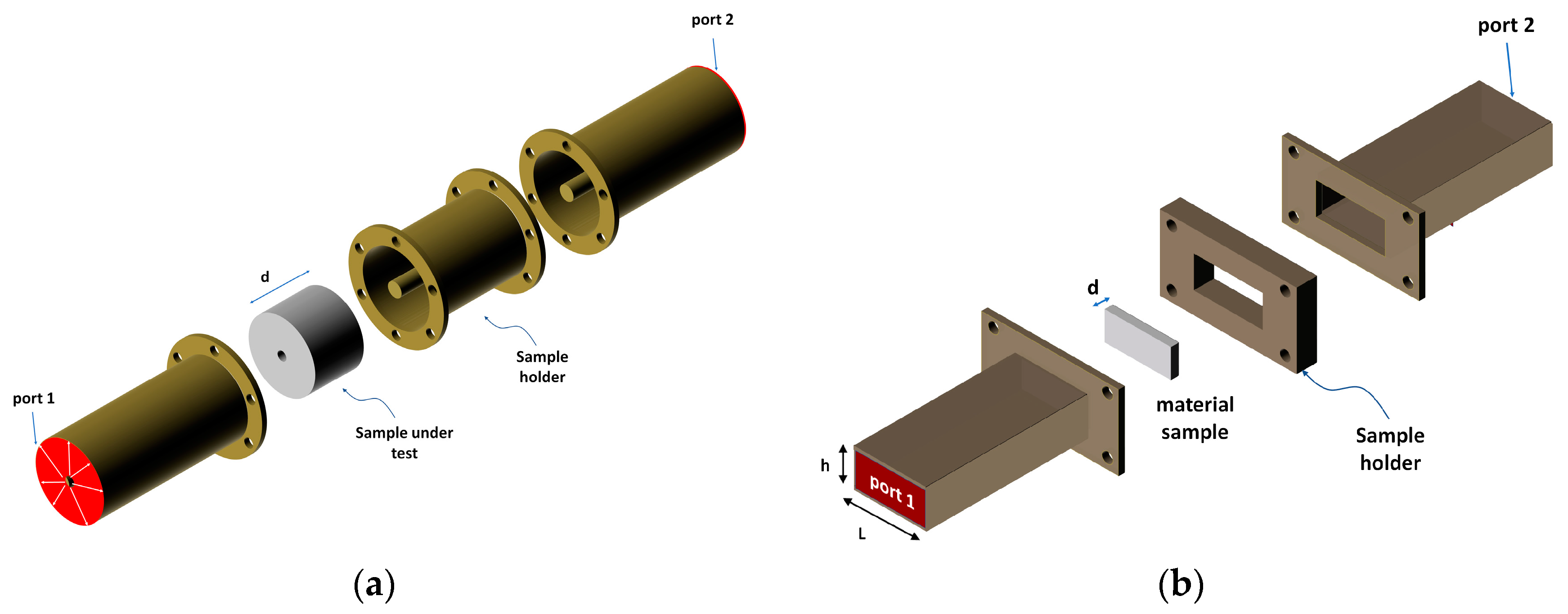
Figure 3.
Transmission and reflection coefficient: (a) amplitude; (b) phase of a rectangular sample of 8 mm thickness with εr = 9 − j0, µr = 1 − j0.
Figure 3.
Transmission and reflection coefficient: (a) amplitude; (b) phase of a rectangular sample of 8 mm thickness with εr = 9 − j0, µr = 1 − j0.

Figure 4.
Estimated electric permittivity and magnetic permeability for a dielectric sample of 8 mm with εr = 9 − j0, µr = 1 − j0 in the case of n = 0 (a,b) and n = 1 (c,d).
Figure 4.
Estimated electric permittivity and magnetic permeability for a dielectric sample of 8 mm with εr = 9 − j0, µr = 1 − j0 in the case of n = 0 (a,b) and n = 1 (c,d).
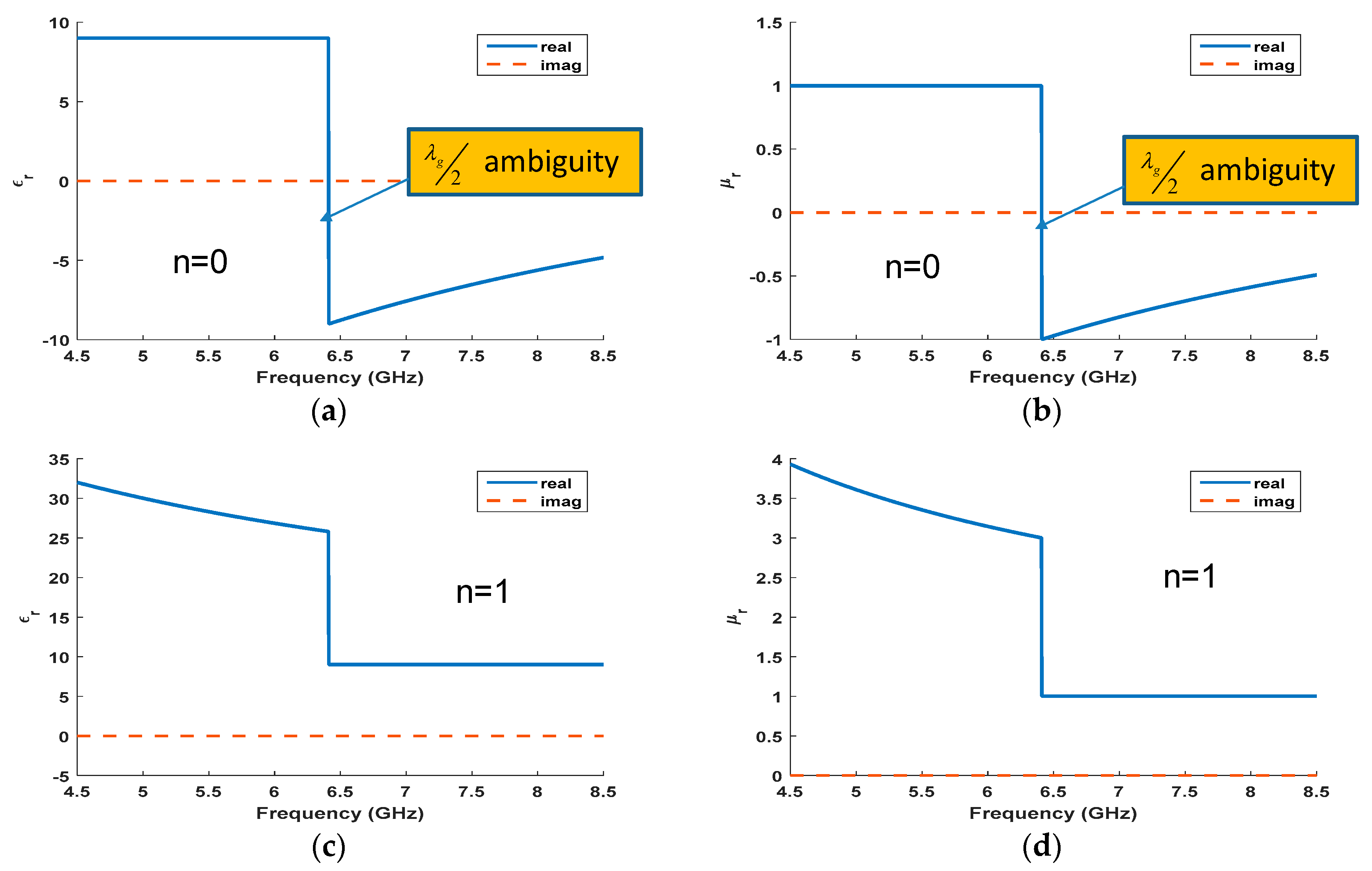
Figure 5.
Propagation constant of the medium with NRW with n = 0 (a) and with the stepwise method (b).
Figure 5.
Propagation constant of the medium with NRW with n = 0 (a) and with the stepwise method (b).
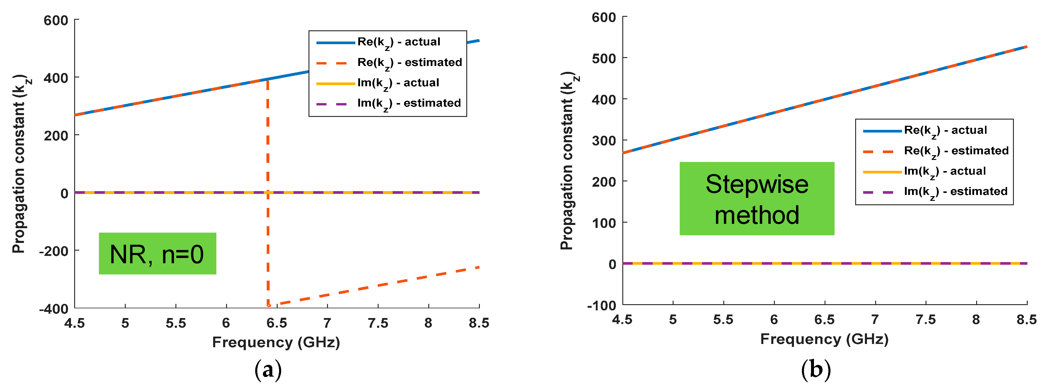
Figure 6.
(a) Scattering parameters for a sample of εr = 30 − j0.2, µr = 1 − j0 with d = 8 mm; (b) estimated dielectric permittivity for n = 0 and n = 1.
Figure 6.
(a) Scattering parameters for a sample of εr = 30 − j0.2, µr = 1 − j0 with d = 8 mm; (b) estimated dielectric permittivity for n = 0 and n = 1.

Figure 7.
Scattering parameters for a sample of εr = 9 − j0.2, µr = 1 − j0 with d = 8 mm perturbed by Additive White Gaussian Noise (AWGN) with mean value mυ = 0 and standard deviation (a,b); estimated dielectric permittivity and magnetic permeability for n = 0 for the first frequency point and stepwise algorithm (c,d).

Figure 8.
Representation of the convergence of the algorithm on the complex space of the dielectric permittivity. The searched values are (a) εR = 20 − j10 and (b).εR = 6.15 − j0.0184.
Figure 8.
Representation of the convergence of the algorithm on the complex space of the dielectric permittivity. The searched values are (a) εR = 20 − j10 and (b).εR = 6.15 − j0.0184.

Figure 9.
Real and imaginary parts as a function of the frequency of the electric permittivity in the case of the Debye (a) and Lorentz (b) models.
Figure 9.
Real and imaginary parts as a function of the frequency of the electric permittivity in the case of the Debye (a) and Lorentz (b) models.
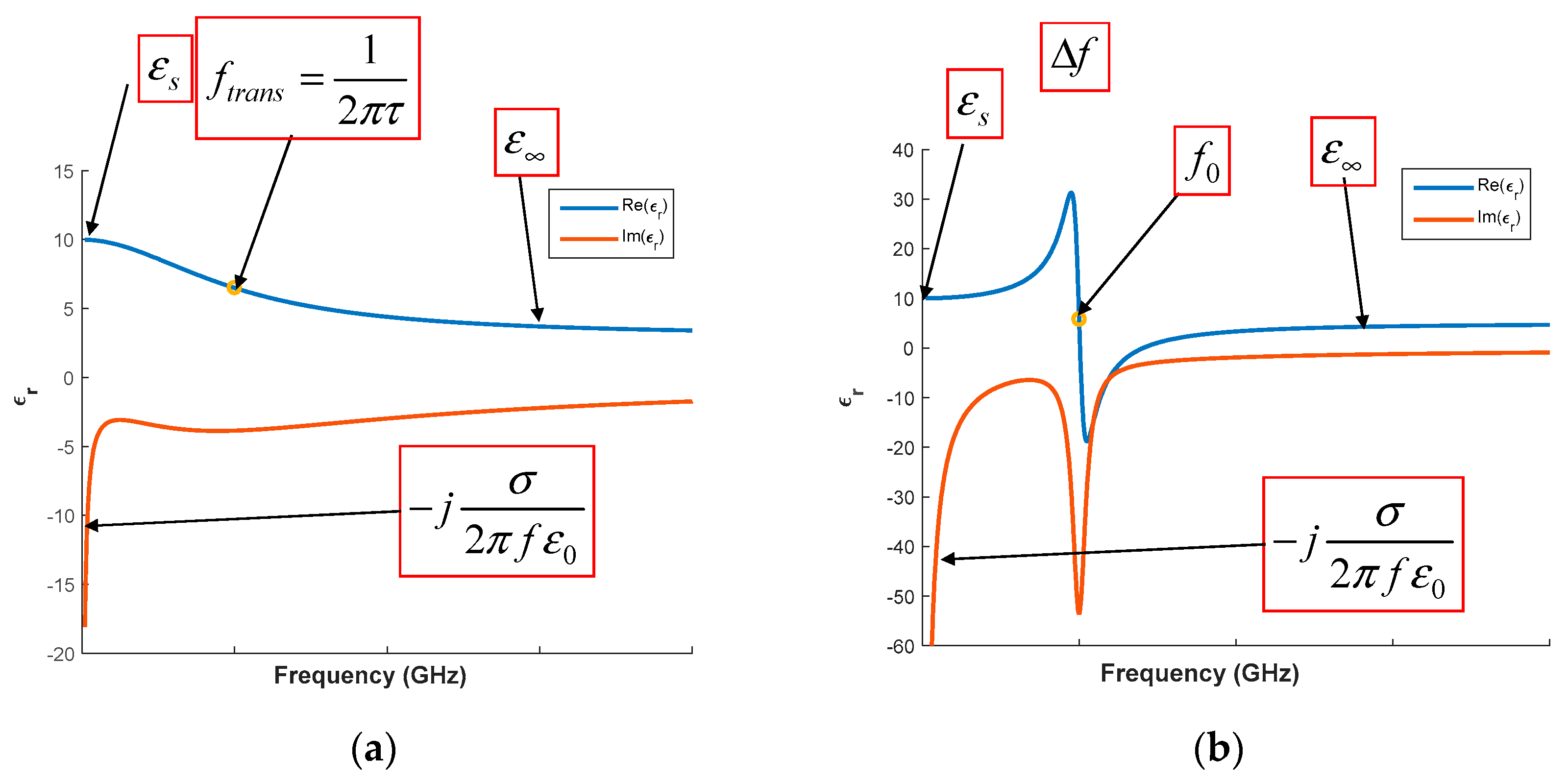
Figure 10.
Real and imaginary parts of the dielectric permittivity estimated with NRW and the iterative method employing the Debye dispersion model with μr = 1 for the case of a dielectric sample with thickness equal to 10 cm (a) and 15 cm (b). In this case, the processed data are not affected by noise.
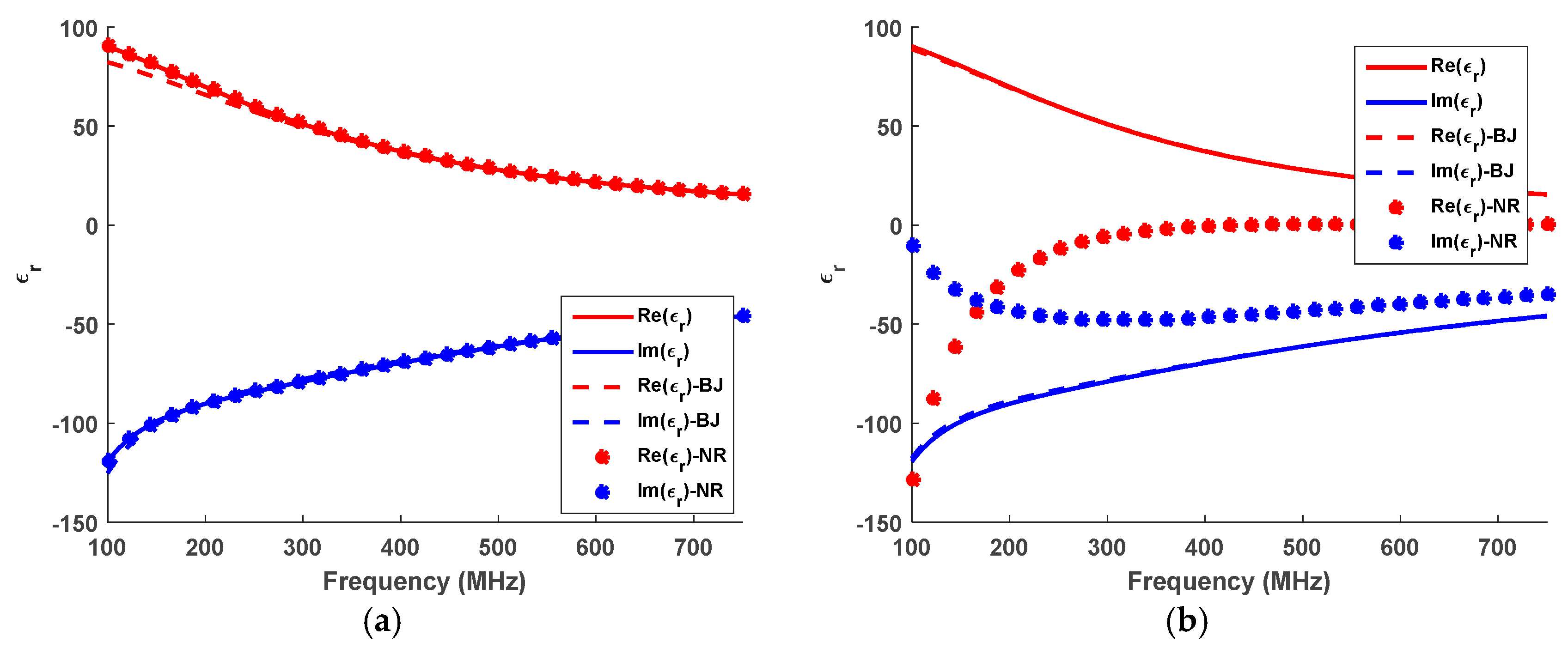
Figure 11.
Comparison between the NRW and iterative method (BJ) employing the Debye dispersion model for the estimation of the dielectric permittivity with μr = 1. (a) Measured, downsampled and GA-estimated S-parameters for the case of a dielectric sample with thickness equal to 10 cm; (b) estimated dielectric permittivity with the two methods. In this case the processed data are affected by AWGN noise with mv = 0 and σ = 0.01.
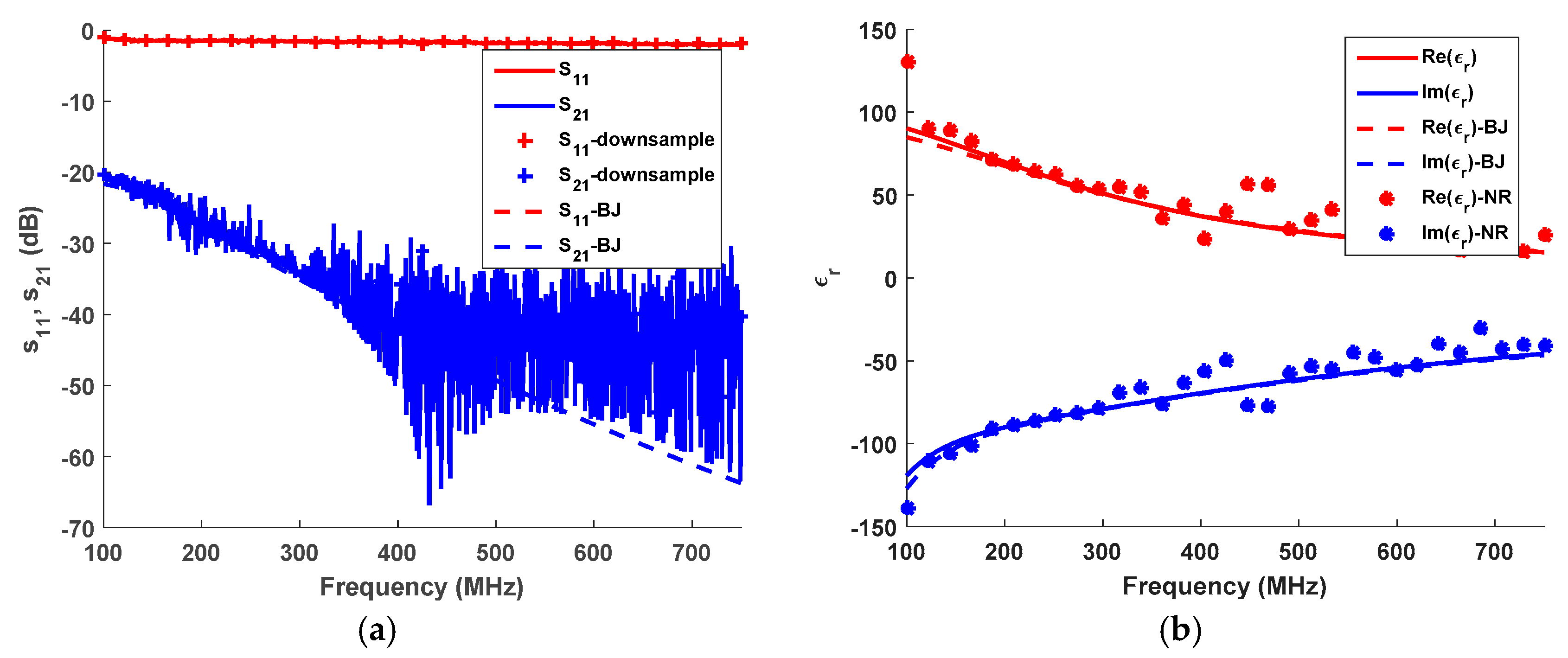
Figure 12.
Real and imaginary parts of the (a) dielectric permittivity and (b) magnetic permittivity estimated with NRW and the iterative method (BJ) employing the Debye dispersion model with μr = 3 for the case of a dielectric sample with thickness equal to 10 cm. In this case, the processed data are affected by AWGN noise with mv = 0 and σ = 0.01.

Figure 13.
(a) Resonant measurement setup in a waveguide based on FSS filters; (b) estimation principle.
Figure 13.
(a) Resonant measurement setup in a waveguide based on FSS filters; (b) estimation principle.
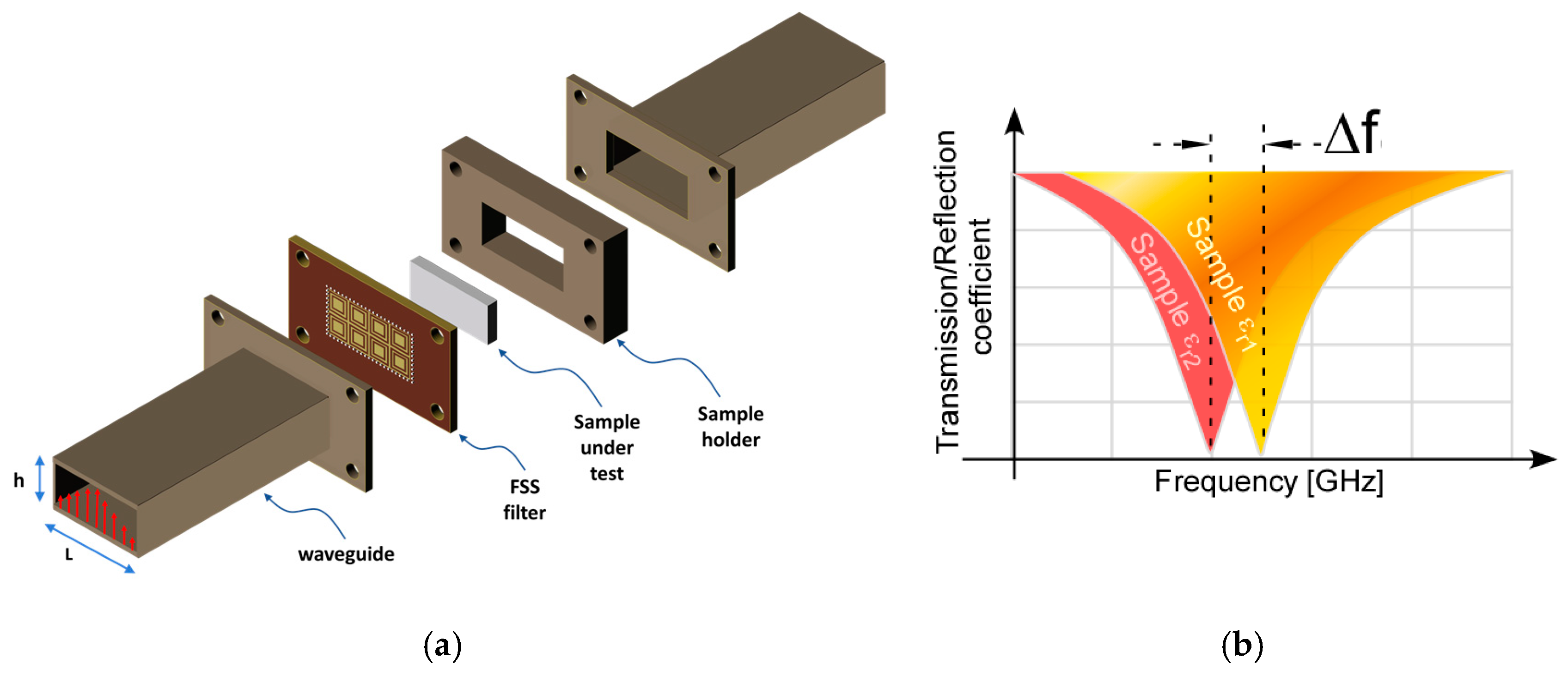
Figure 14.
(a) Shift-permittivity map: unknown dielectric permittivity as a function of the frequency shift of the resonant peak; (b) maximum value of the measurable dielectric permittivity as a function of the sample thickness.
Figure 14.
(a) Shift-permittivity map: unknown dielectric permittivity as a function of the frequency shift of the resonant peak; (b) maximum value of the measurable dielectric permittivity as a function of the sample thickness.
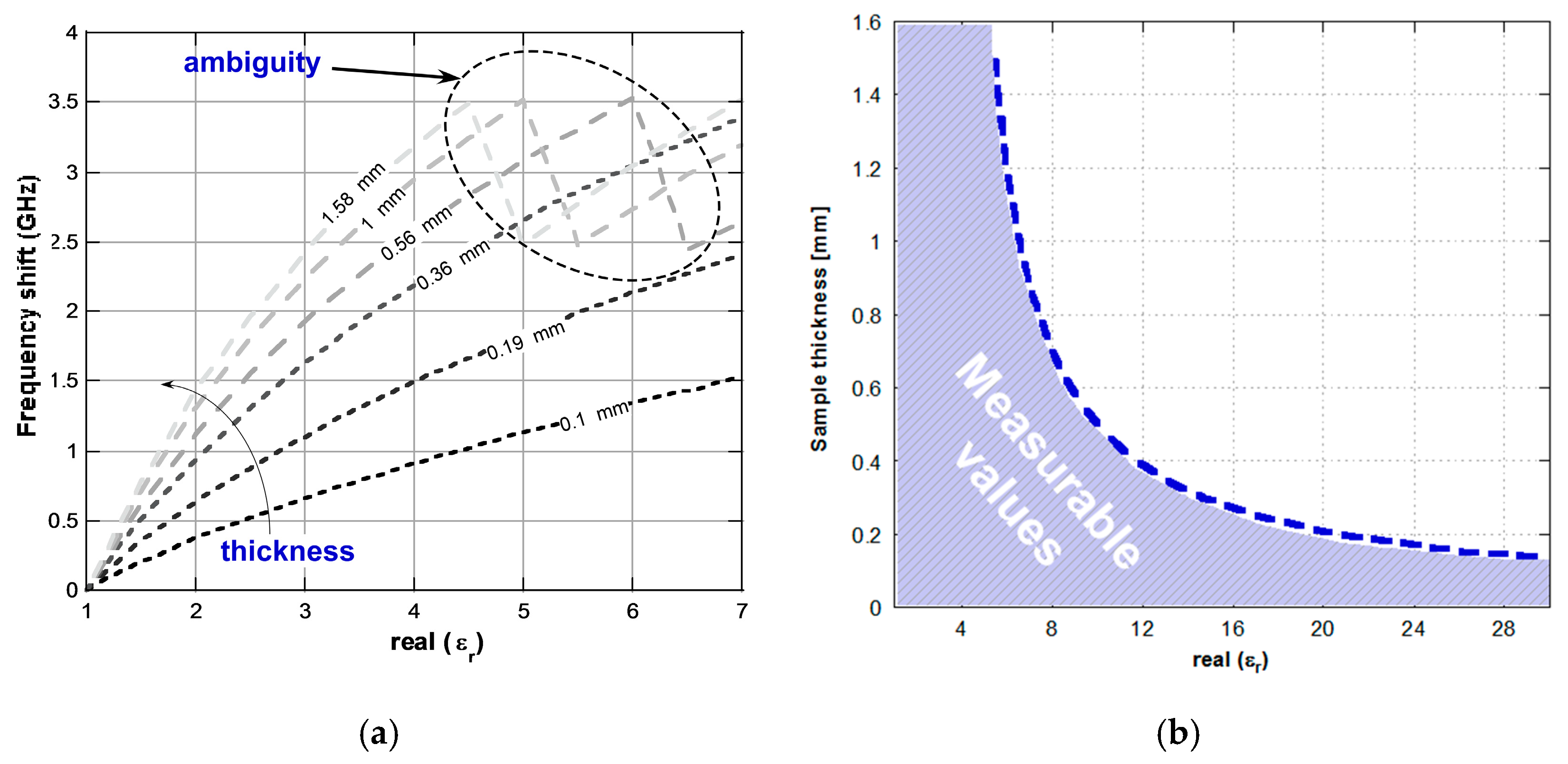
Figure 15.
(a) Transmission line model of a thin dielectric slab with characteristic impedance ; (b) transmission line model of an infinitesimal sheet characterised by a surface impedance Zs.
Figure 15.
(a) Transmission line model of a thin dielectric slab with characteristic impedance ; (b) transmission line model of an infinitesimal sheet characterised by a surface impedance Zs.

Figure 16.
(a) Equivalent surface impedance to verify the equivalence of the thin sheet with a finite dielectric conductivity (Figure 15b) and the infinitesimally thin sheet characterised by a lumped impedance (Figure 15a). (b) Behaviour of the kd term and the good conductor condition as a function of frequency.

Figure 17.
(a) Measurement setup and (b) simplified transmission line model.

Figure 18.
Estimated surface resistance of an ink deposition with a DC surface resistance of 20 ohm/sq (a). The substrate is FR4 with a thickness of 1.6 mm. The results are obtained by using setup 1 (b) and setup 2 (c).
Figure 18.
Estimated surface resistance of an ink deposition with a DC surface resistance of 20 ohm/sq (a). The substrate is FR4 with a thickness of 1.6 mm. The results are obtained by using setup 1 (b) and setup 2 (c).
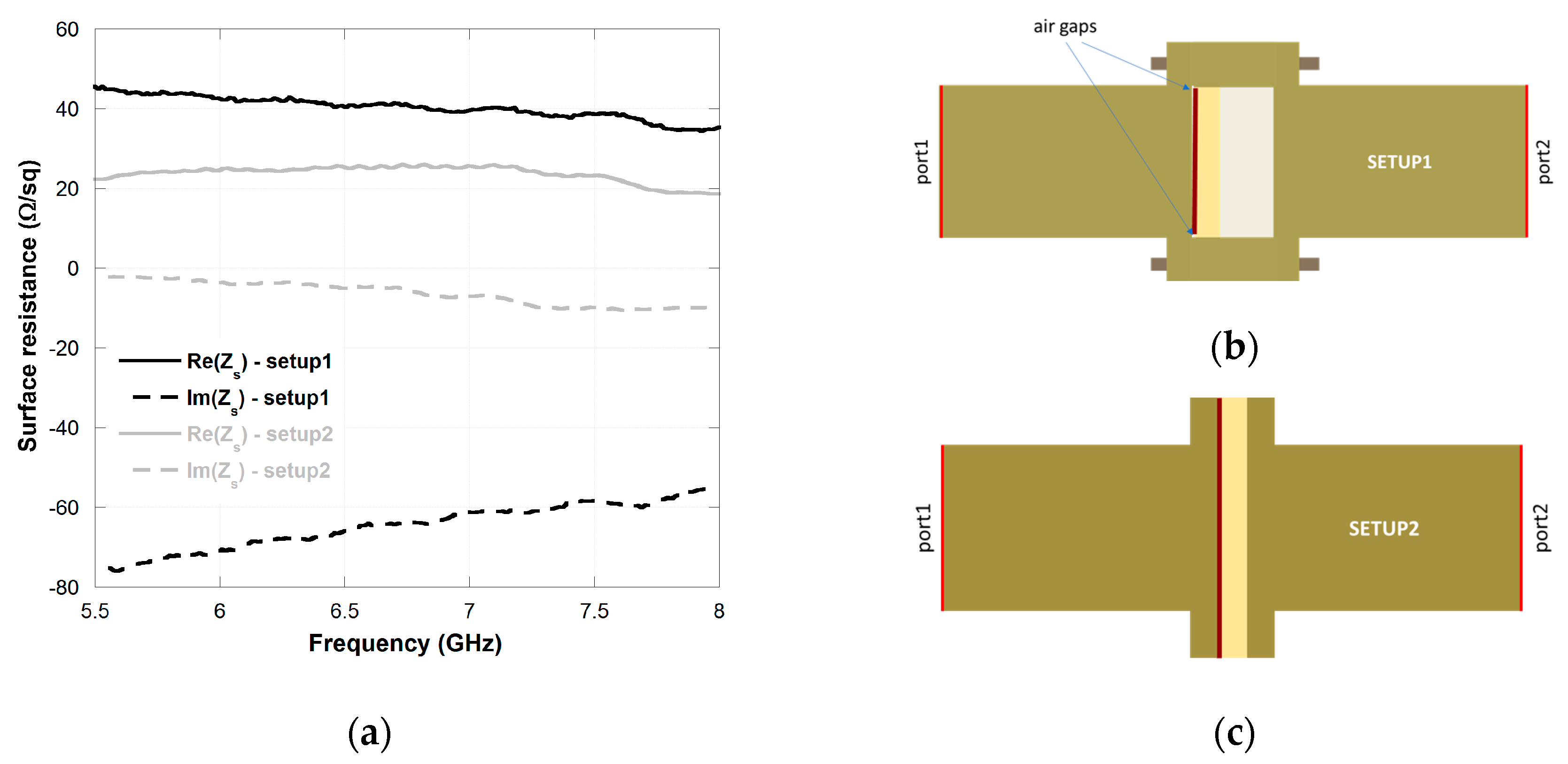
Figure 19.
Equivalent circuit of the waveguide junction in the absence (a) or presence (b) of the impedance sheet.
Figure 19.
Equivalent circuit of the waveguide junction in the absence (a) or presence (b) of the impedance sheet.
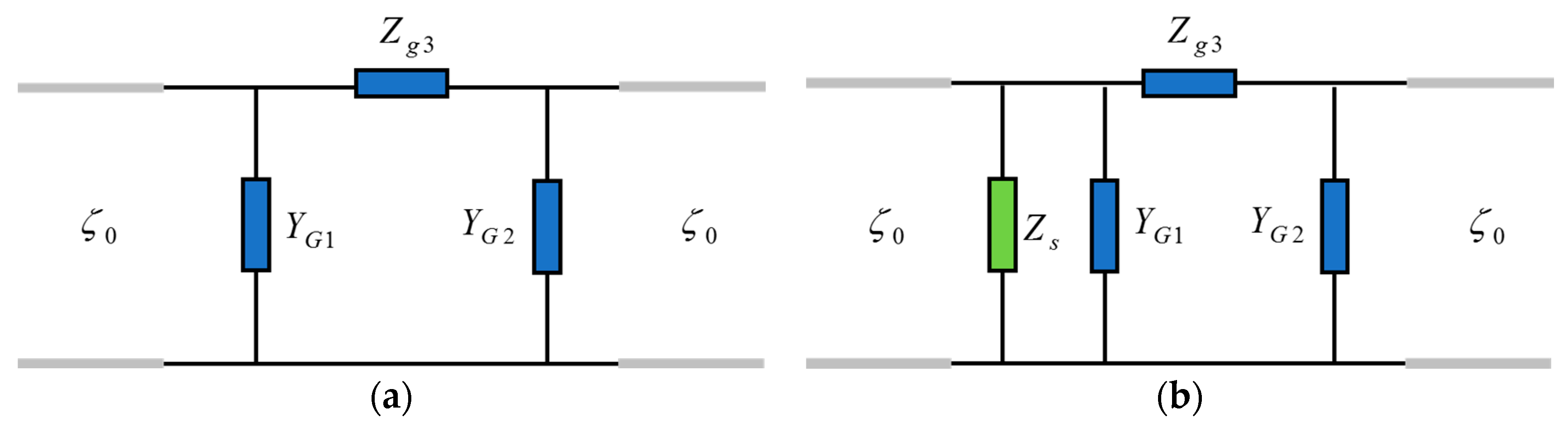
Figure 20.
Measurement setup simulated with Ansys Electronics v. 16: (a) side view; (b) front view.

Figure 21.
Estimated surface impedance (real and imaginary part) for three different thicknesses of the substrate: Zs was set to 20 + j0 in the simulations performed with Ansys Electronics v. 16. Closed: sample entirely contained in a closed waveguide. Size 1: Δx = 2 mm, Δy = 2 mm, Size 2: Δx = 6 mm, Δy = 4 mm. (a,b) d = 0.5 mm, (c,d) d = 1.5 mm, (e,f) d = 2.5 mm.


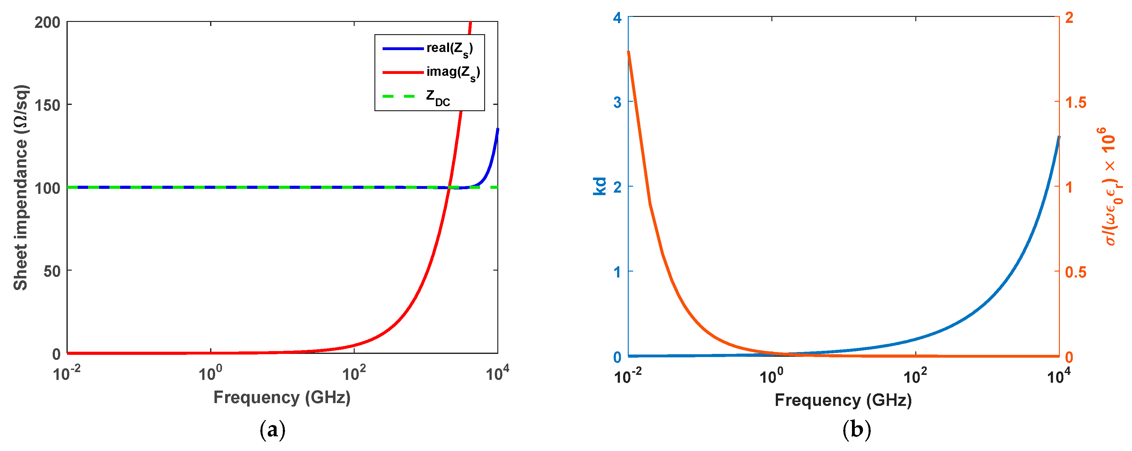
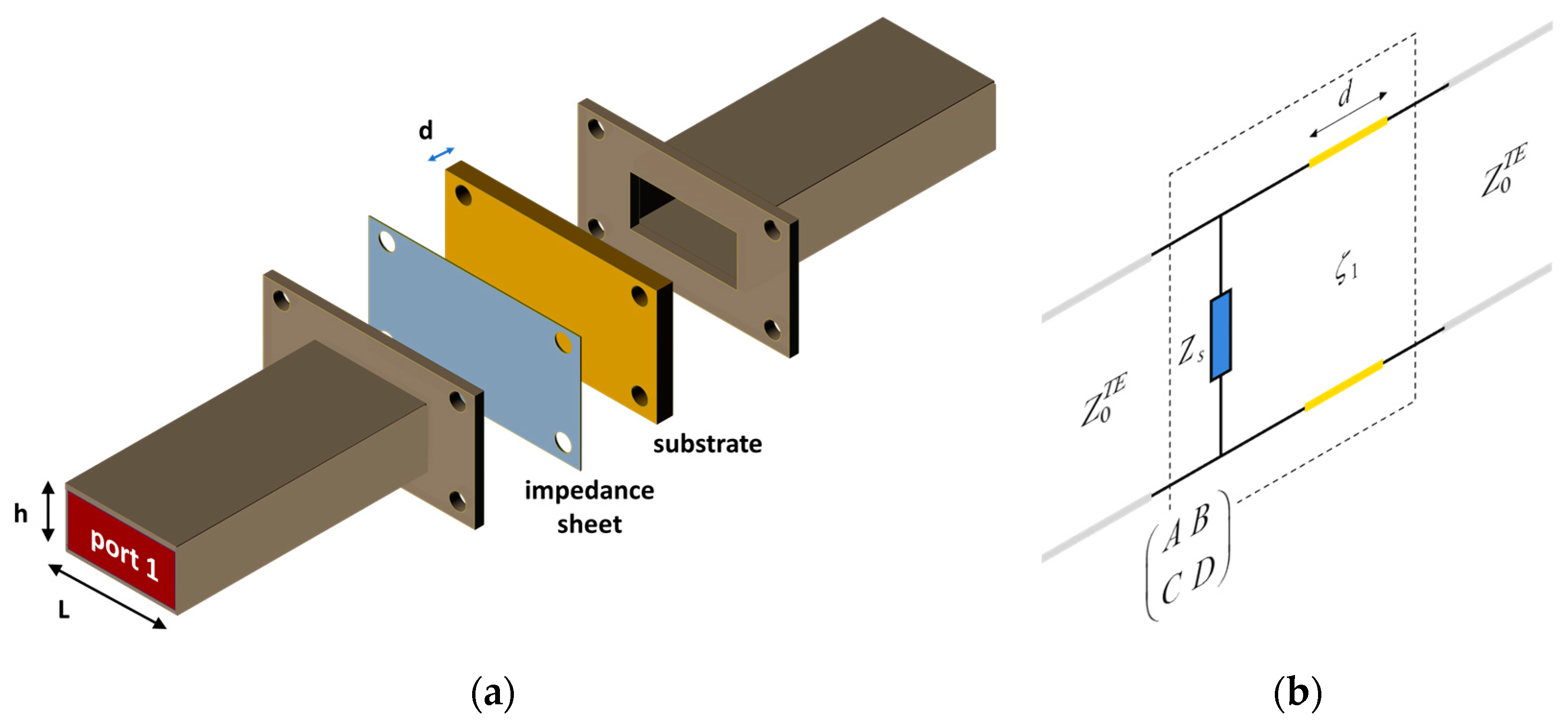
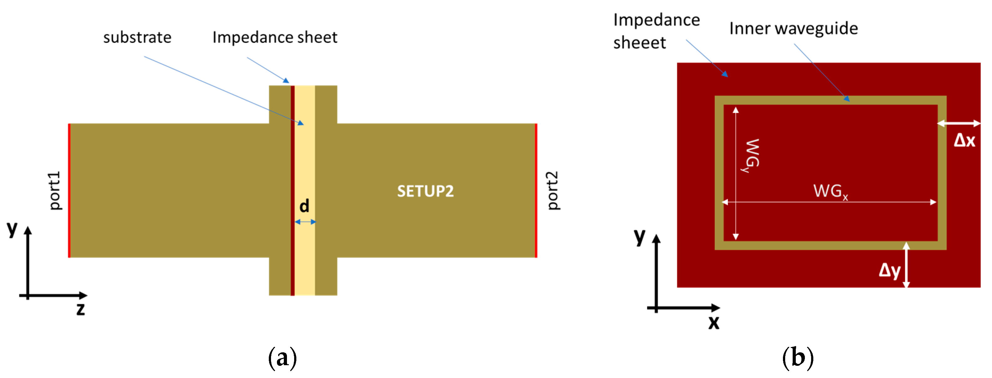
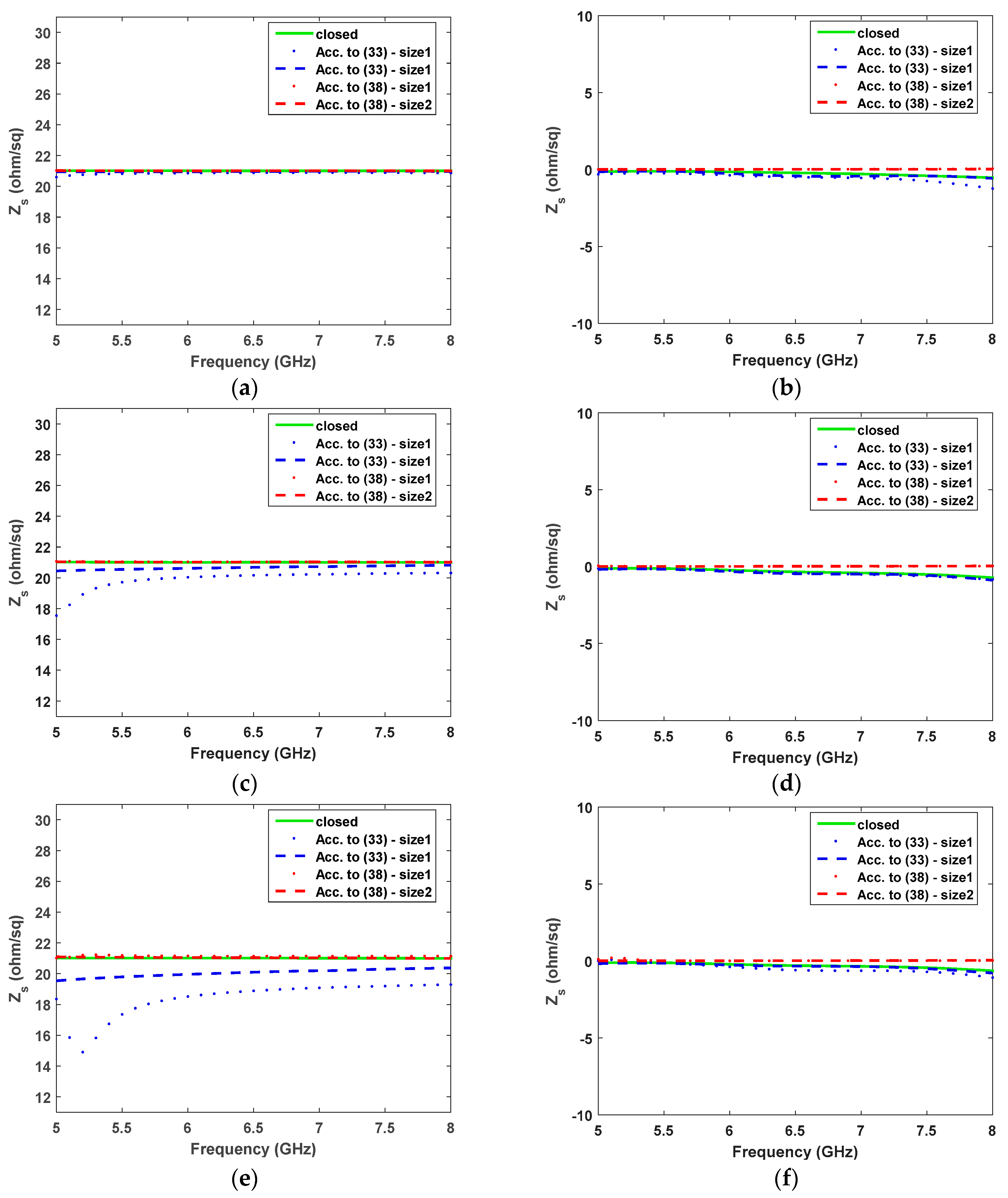
Table 1.
Electrical and geometrical parameters of the material characterised by a Debye dispersion.
| εs | ε | ftrans [MHz] | σ | µ | t [mm] | |
|---|---|---|---|---|---|---|
| Actual values | 100 | 2 | 300 | 0.5 | 1 | 100 |
| Best values (3 runs) | 87 | 1.43 | 305 | 0.64 | 1.01 | 100 |
| Actual values | 100 | 2 | 300 | 0.5 | 1 | 150 |
| Best values (6 runs) | 97.9 | 1.1 | 305 | 0.49 | 1.0 | 150 |
| GA search space (min) | 1 | 1 | 1 | 0 | 1 | |
| GA search space (max) | 200 | 50 | 1000 | 10 | 5 |
Table 2.
Advantages and disadvantages of the direct inversion procedure based on the Nicolson-Ross-Weir algorithm and the Baker–Jarvis iterative search based on the S-parameters cost function.
Table 2.
Advantages and disadvantages of the direct inversion procedure based on the Nicolson-Ross-Weir algorithm and the Baker–Jarvis iterative search based on the S-parameters cost function.
| Advantages | Disadvantages | Computation Time | |
|---|---|---|---|
| Nicolson Ross Weir direct inversion |
|
| Immediate |
| Baker-Jarvis iterative search |
|
| ∼1 min |
| Resonant Methods |
|
| Immediate |
© 2017 by the authors. Licensee MDPI, Basel, Switzerland. This article is an open access article distributed under the terms and conditions of the Creative Commons Attribution (CC BY) license (http://creativecommons.org/licenses/by/4.0/).
Share and Cite
MDPI and ACS Style
Costa, F.; Borgese, M.; Degiorgi, M.; Monorchio, A. Electromagnetic Characterisation of Materials by Using Transmission/Reflection (T/R) Devices. Electronics 2017, 6, 95. https://doi.org/10.3390/electronics6040095
AMA Style
Costa F, Borgese M, Degiorgi M, Monorchio A. Electromagnetic Characterisation of Materials by Using Transmission/Reflection (T/R) Devices. Electronics. 2017; 6(4):95. https://doi.org/10.3390/electronics6040095
Chicago/Turabian StyleCosta, Filippo, Michele Borgese, Marco Degiorgi, and Agostino Monorchio. 2017. "Electromagnetic Characterisation of Materials by Using Transmission/Reflection (T/R) Devices" Electronics 6, no. 4: 95. https://doi.org/10.3390/electronics6040095
Note that from the first issue of 2016, this journal uses article numbers instead of page numbers. See further details here.